EP0849980A1 - An x-ray imaging system using an image detector - Google Patents
An x-ray imaging system using an image detector Download PDFInfo
- Publication number
- EP0849980A1 EP0849980A1 EP97310304A EP97310304A EP0849980A1 EP 0849980 A1 EP0849980 A1 EP 0849980A1 EP 97310304 A EP97310304 A EP 97310304A EP 97310304 A EP97310304 A EP 97310304A EP 0849980 A1 EP0849980 A1 EP 0849980A1
- Authority
- EP
- European Patent Office
- Prior art keywords
- aec
- array
- ray
- image detector
- image
- Prior art date
- Legal status (The legal status is an assumption and is not a legal conclusion. Google has not performed a legal analysis and makes no representation as to the accuracy of the status listed.)
- Granted
Links
- 238000003384 imaging method Methods 0.000 title description 15
- 239000007787 solid Substances 0.000 claims abstract description 4
- 238000000034 method Methods 0.000 description 7
- 239000002131 composite material Substances 0.000 description 5
- 230000004907 flux Effects 0.000 description 2
- 230000001965 increasing effect Effects 0.000 description 2
- 230000005855 radiation Effects 0.000 description 2
- XUIMIQQOPSSXEZ-UHFFFAOYSA-N Silicon Chemical compound [Si] XUIMIQQOPSSXEZ-UHFFFAOYSA-N 0.000 description 1
- 238000010521 absorption reaction Methods 0.000 description 1
- 229910021417 amorphous silicon Inorganic materials 0.000 description 1
- 210000003484 anatomy Anatomy 0.000 description 1
- 230000015572 biosynthetic process Effects 0.000 description 1
- 238000010276 construction Methods 0.000 description 1
- 238000010586 diagram Methods 0.000 description 1
- 238000005516 engineering process Methods 0.000 description 1
- 230000002708 enhancing effect Effects 0.000 description 1
- 239000011521 glass Substances 0.000 description 1
- 238000004806 packaging method and process Methods 0.000 description 1
- 230000035945 sensitivity Effects 0.000 description 1
- 229910052710 silicon Inorganic materials 0.000 description 1
- 239000010703 silicon Substances 0.000 description 1
- 239000000758 substrate Substances 0.000 description 1
- 238000001429 visible spectrum Methods 0.000 description 1
Images


Classifications
-
- A—HUMAN NECESSITIES
- A61—MEDICAL OR VETERINARY SCIENCE; HYGIENE
- A61B—DIAGNOSIS; SURGERY; IDENTIFICATION
- A61B6/00—Apparatus for radiation diagnosis, e.g. combined with radiation therapy equipment
- A61B6/54—Control of apparatus or devices for radiation diagnosis
- A61B6/542—Control of apparatus or devices for radiation diagnosis involving control of exposure
-
- H—ELECTRICITY
- H05—ELECTRIC TECHNIQUES NOT OTHERWISE PROVIDED FOR
- H05G—X-RAY TECHNIQUE
- H05G1/00—X-ray apparatus involving X-ray tubes; Circuits therefor
- H05G1/08—Electrical details
- H05G1/26—Measuring, controlling or protecting
- H05G1/30—Controlling
- H05G1/38—Exposure time
- H05G1/42—Exposure time using arrangements for switching when a predetermined dose of radiation has been applied, e.g. in which the switching instant is determined by measuring the electrical energy supplied to the tube
- H05G1/44—Exposure time using arrangements for switching when a predetermined dose of radiation has been applied, e.g. in which the switching instant is determined by measuring the electrical energy supplied to the tube in which the switching instant is determined by measuring the amount of radiation directly
Definitions
- the field of the invention is x-ray imaging systems, and particularly, automatic exposure control for x-ray systems.
- AEC Automatic exposure control
- the AEC develops a signal proportional to the x-ray flux into the image receptor. This signal is used to regulate the total exposure for each image either by terminating the exposure or by adjusting the x-ray flux rate.
- the ion chamber detector can be composed of several separate chambers, in which case the exposure-control signal can come from any single chamber or a combination of chambers.
- One disadvantage of this type of detector is that some of the radiation that would otherwise contribute to signal in the image receptor is lost because of attenuation in the ion chamber.
- Such chambers must also be carefully constructed so that any variation in absorption over their area is small enough to preclude artifacts in the detected image.
- an ion chamber is placed behind the image receptor. In this position it does not intercept x-rays used for imaging, but the available radiation, and thus the signal in the ion chamber, is reduced because of attenuation in the image receptor and any associated packaging or shielding.
- the thickness of the ion chamber could be increased to increase its sensitivity, but this could make the imaging system more bulky.
- Some AEC systems employ a scintillating screen coupled to a light sensor in place of the ion chamber.
- Another AEC method which is used with image intensifier based systems, collects some of the light from the image gate at the output of the image intensifier and detects the brightness level with a photosensor.
- a disadvantage of this AEC method is that the light-pickup device is placed in the image path. This can lead to interference of the image by the pickup device in some imaging situations.
- X-ray imaging systems which employ a large area solid state x-ray detector, such as that described in U.S. patent No. 4,996,413 entitled "Apparatus And Method For Reading Data from An Image Detector", cannot use the AEC method employed in image intensifier systems. Unlike an image intensifier system, there is no minified light image from which light can be conveniently collected. Also, one of the design objectives when using large area solid state detectors is to reduce the bulk of the detector package. This makes the use of an ion chamber placed in front of or behind the image detector less desirable.
- an x-ray system using an image detector comprising: an array of photosensors disposed behind the image detector and positioned to detect photons passing through the image detector; means for combining currents produced by photosensors in said array; an integrator connected to the means for combining for providing an AEC signal; and an exposure control connected to receive the AEC signal and employ the same to control x-ray exposure.
- an AEC detector is used containing an array of photosensors disposed behind the image detector to detect the x-rays and/or light passing therethrough.
- the number and location of the photosensors used for exposure control, the AEC "field of view" can be adjusted for different imaging procedures by selectively combining the photosensor signals to detect x-rays and/or light from one or more regions of the desired shape and size.
- the invention seeks to provide an AEC signal without producing image artifacts or significantly increasing the size of the detector package.
- the photosensor array is disposed behind the image receptor and will not, therefore, interfere with the image formation.
- the photosensor array may be constructed using a number of different technologies, which result in a minimal increase in the size of the detector package.
- the invention seeks to provide an AEC signal from a field of view that can be selectively adjusted.
- a selector circuit combines the signals from each array photosensor and the field of view can be adjusted by selecting which signals are included in the combination.
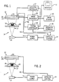
- an x-ray apparatus 14 includes an x-ray tube 15 which, when excited by a power supply 16, emits an x-ray beam 17. As illustrated, the x-ray beam is directed toward a patient 18 lying on an x-ray transmissive table 20. The portion of the beam which is transmitted through the table and the patient impinges upon an x-ray detector assembly 22.
- the x-ray detector assembly 22 comprises a scintillator 24 that converts the x-ray photons to lower energy photons in the visible spectrum. Contiguous with the scintillator 24 is an image photodetector array 26, which converts the light photons into an electrical signal.
- a detector controller 27 contains electronics for operating the detector array 26 to acquire an image and to read out the signal from each photodetector element.
- the output signal from the image photodetector array 26 is coupled to an image processor 28 that includes circuitry for collecting, processing and enhancing the x-ray image signal.
- the processed image is displayed on a video monitor 32 and may be stored in an image storage device 30.
- the overall operation of the x-ray apparatus 14 is governed by a system controller 36 which receives commands from the user via an operator interface panel 38.
- the image photodetector array 26 consists of amorphous silicon devices on a glass substrate. A portion of the light from the scintillator 24 is transmitted through these silicon devices and through the spaces between them. In addition, some of the x-rays are transmitted through both the scintillator 24 and the image photodetector array 26.
- the AEC photosensor array 23 of the present invention may also be used in a second preferred embodiment, illustrated in Fig. 2, in which it is used with a film/screen imaging sensor 25.
- the AEC detector consists of a scintillator 21 coupled to a photosensor array 23.
- the scintillator 21 is used to absorb x-rays transmitted through the film/screen sensor 25 and produce light photons which are absorbed by the photosensors in the AEC photosensor array 23.
- the operation of the AEC photosensor array 23 is the same as in the first preferred embodiment.
- the AEC photosensor array 23 is a photodiode array 50.
- the photodiode array 50 is disposed behind the imaging detector from which the exposure is to be monitored for the purpose of exposure control. Light which impinges on the surface of the photodiode array 50 creates electron-hole pairs in the photodiodes it strikes, and this produces a current when connected to an external circuit. The signal created from the array 50 is used for automatic exposure control.
- the arrangement of the elements in the array 50 is designed to enable x-ray intensity to be monitored for specific anatomical areas as may be required by the particular examination being performed as well as the size of the field of view.
- a preferred embodiment of the photodiode array 50 is shown in Fig. 4.
- the photodiodes in the array 50 are assembled into regions designated 1-16. All of the photodiodes in each region have their outputs connected together to provide a regional signal.
- One of sixteen output leads 52 connects to each region to bring out the regional signal from the photodiodes therein. It should be apparent from Fig. 4, that by selectively combining the regional signals on the sixteen leads 52, the size and shape of the area from which the AEC signals are gathered can be changed.
- Region 1 occupies a central, square area, and the remaining regions 2-16 enable the size and shape of this central area to be expanded outward.
- the AEC photodiode array 50 in Fig. 4 is used with a 20 cm by 20 cm imaging detector.
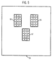
- the size of the array and the location and grouping of the diodes will be different for other imaging detectors. In particular, some detectors require the diodes to be grouped into disconnected areas, possibly of different sizes and shapes.
- Fig. 5 shows an example of such an AEC photodiode array 54 which includes three separate sense areas 55, 56 and 57. This grouping of diodes mimics the geometry of the particular ion chamber AEC detector used with 35 by 43 centimeter film/screen imaging detectors.
- the signals on leads 52 are separately amplified at 54.
- the signal from each region is proportional to the exposure in that region times the area of the region. If the control signal is desired to contain equal weighting from throughout the control area, the gain of each amplifier is adjusted to be inversely proportional to the area of its region. Alternatively, if the weighting of some parts of the control area is desired to be greater than other parts, the gains can be appropriately adjusted.
- the sixteen amplified signals are then applied to a selector 56 which receives a selection control signal 58 that indicates which ones of the amplified signals are to be combined to form the composite AEC signal.
- the selector 56 is comprised of analog switches.
- the selection control signal is determined by the selected field of view of the image and the type of patient examination selected by the operator and it is produced by the system controller 36 (Fig. 1).
- the selected signals are applied to a summing and signal scaling amplifier 60 which combines them and then scales the resulting composite AEC signal in inverse proportion to the number of regions selected. While this composite analog AEC signal may be integrated and used to control x-ray exposure directly, in the preferred embodiment the composite AEC signal is digitized by an analog-to-digital converter 62.
- the digitized composite AEC signal is integrated as shown at 64 and used to control exposure as described above.
- circuit of Fig. 3 can be modified to digitize the analog signals from each region prior to being combined. This enables the weighting and combining functions to be performed digitally.
Abstract
Description
Claims (7)
- An x-ray system using an image detector, comprising:an array of photosensors disposed behind the image detector and positioned to detect photons passing through the image detector;means for combining currents produced by photosensors in said array;an integrator connected to the means for combining for providing an AEC signal; andan exposure control connected to receive the AEC signal and employ the same to control x-ray exposure.
- A system as recited in claim 1 in which the means for combining includes a selector that selects photosensor currents to be combined.
- A system as recited in claim 2 which includes a system controller that operates said selector to determine the area over which the AEC signal is to be acquired.
- A system as recited in claim 1, 2 or 3 which the image detector is a large area solid state image detector.
- A system as recited in any preceding claim in which photosensors in each of a plurality of regions in the array are connected together such that their currents are summed together to form regional signals.
- A system as recited in claim 5 in which the means for combining includes a selector that selects regional signals to be combined in response to a selection control signal.
- A system as recited in claim 1 in which the means for combining includes means for scaling the AEC signal based on the number of photosensor currents combined.
Applications Claiming Priority (2)
| Application Number | Priority Date | Filing Date | Title |
|---|---|---|---|
| US771725 | 1996-12-20 | ||
| US08/771,725 US5751783A (en) | 1996-12-20 | 1996-12-20 | Detector for automatic exposure control on an x-ray imaging system |
Publications (2)
| Publication Number | Publication Date |
|---|---|
| EP0849980A1 true EP0849980A1 (en) | 1998-06-24 |
| EP0849980B1 EP0849980B1 (en) | 2005-11-16 |
Family
ID=25092781
Family Applications (1)
| Application Number | Title | Priority Date | Filing Date |
|---|---|---|---|
| EP97310304A Expired - Lifetime EP0849980B1 (en) | 1996-12-20 | 1997-12-19 | An x-ray imaging system using an image detector |
Country Status (4)
| Country | Link |
|---|---|
| US (1) | US5751783A (en) |
| EP (1) | EP0849980B1 (en) |
| JP (1) | JPH10284289A (en) |
| DE (1) | DE69734641T2 (en) |
Cited By (1)
| Publication number | Priority date | Publication date | Assignee | Title |
|---|---|---|---|---|
| WO2018104497A1 (en) * | 2016-12-08 | 2018-06-14 | Visus Health It Gmbh | Detector strip for radiographic film |
Families Citing this family (60)
| Publication number | Priority date | Publication date | Assignee | Title |
|---|---|---|---|---|
| WO1998048599A2 (en) * | 1997-04-24 | 1998-10-29 | Koninklijke Philips Electronics N.V. | Exposure control on the basis of a relevant part of an x-ray image |
| JP4241942B2 (en) * | 1997-06-18 | 2009-03-18 | シーメンス アクチエンゲゼルシヤフト | Imaging dose measurement method and radiation image imaging apparatus |
| FR2771513B1 (en) * | 1997-11-25 | 2000-05-26 | Trixell Sas | PHOTOSENSITIVE DEVICE HAVING ILLUMINATION MEASURING DEVICE |
| US6192105B1 (en) | 1998-11-25 | 2001-02-20 | Communications & Power Industries Canada Inc. | Method and device to calibrate an automatic exposure control device in an x-ray imaging system |
| US6151383A (en) * | 1998-12-30 | 2000-11-21 | General Electric Company | Radiographic testing system with learning-based performance prediction |
| US6540399B1 (en) | 1999-02-26 | 2003-04-01 | Dentsply Research & Development Corp. | Bite block for dental X-Ray procedures |
| US6243441B1 (en) | 1999-07-13 | 2001-06-05 | Edge Medical Devices | Active matrix detector for X-ray imaging |
| US6900442B2 (en) * | 1999-07-26 | 2005-05-31 | Edge Medical Devices Ltd. | Hybrid detector for X-ray imaging |
| US6864484B1 (en) | 1999-07-26 | 2005-03-08 | Edge Medical Devices, Ltd | Digital detector for x-ray imaging |
| US6437338B1 (en) | 1999-09-29 | 2002-08-20 | General Electric Company | Method and apparatus for scanning a detector array in an x-ray imaging system |
| CA2388256A1 (en) | 1999-10-08 | 2001-04-19 | Dentsply International Inc. | Automatic exposure control for dental panoramic and cephalographic x-ray equipment |
| WO2001058148A1 (en) * | 2000-02-02 | 2001-08-09 | Dentsply International Inc. | Automatic x-ray detection for intra-oral dental x-ray imaging apparatus |
| US6404851B1 (en) * | 2000-03-30 | 2002-06-11 | General Electric Company | Method and apparatus for automatic exposure control using localized capacitive coupling in a matrix-addressed imaging panel |
| JP2004504611A (en) * | 2000-03-31 | 2004-02-12 | コーニンクレッカ フィリップス エレクトロニクス エヌ ヴィ | FDXD detector for detecting dose |
| WO2002021822A2 (en) * | 2000-09-02 | 2002-03-14 | Emageon, Inc. | Methods and apparatus for streaming dicom images through data element sources and sinks |
| US6459765B1 (en) | 2000-12-28 | 2002-10-01 | Ge Medical Systems Global Technology Company, Llc | Automatic exposure control and optimization in digital x-ray radiography |
| US6914958B2 (en) | 2001-07-06 | 2005-07-05 | Ge Medical Systems Global Technology Company, Llc | Multi-plane acquisition in digital x-ray radiography |
| US6784433B2 (en) * | 2001-07-16 | 2004-08-31 | Edge Medical Devices Ltd. | High resolution detector for X-ray imaging |
| US7016461B2 (en) * | 2001-07-25 | 2006-03-21 | Gendex Corporation | Real-time digital x-ray imaging apparatus |
| US6895077B2 (en) * | 2001-11-21 | 2005-05-17 | University Of Massachusetts Medical Center | System and method for x-ray fluoroscopic imaging |
| FR2834572B1 (en) * | 2002-01-08 | 2004-07-09 | Ge Med Sys Global Tech Co Llc | RADIOLOGICAL IMAGING SYSTEM, MEDICAL SYSTEM COMPRISING A PLURALITY OF INTERNAL CLOCKS AND SYNCHRONIZATION METHOD |
| EP1551302B1 (en) * | 2002-07-25 | 2012-02-08 | Gendex Corporation | Real-time digital x-ray imaging apparatus and method |
| JP4387644B2 (en) * | 2002-08-05 | 2009-12-16 | キヤノン株式会社 | Method and apparatus for determining dose of X-rays irradiated to subject |
| US7006598B2 (en) * | 2002-08-09 | 2006-02-28 | Canon Kabushiki Kaisha | Imaging method and apparatus with exposure control |
| US7148487B2 (en) | 2002-08-27 | 2006-12-12 | Canon Kabushiki Kaisha | Image sensing apparatus and method using radiation |
| JP2004337343A (en) * | 2003-05-15 | 2004-12-02 | Fuji Photo Film Co Ltd | Radiation dose detector |
| US7105828B2 (en) * | 2004-02-10 | 2006-09-12 | Ge Medical Systems Global Technology Company, Llc | Hybrid x-ray detector |
| CA2574679C (en) | 2004-07-20 | 2013-06-04 | Medtronic, Inc. | Implantable cerebral spinal fluid drainage device and method of draining cerebral spinal fluid |
| FI119968B (en) * | 2005-09-15 | 2009-05-29 | Planmed Oy | Auto Exposure Method and System |
| US7477727B1 (en) | 2006-01-26 | 2009-01-13 | Karl Adolf Malashanko | Digital X-ray image detector array |
| WO2007148262A1 (en) * | 2006-06-22 | 2007-12-27 | Philips Intellectual Property & Standards Gmbh | X-ray image apparatus and method of imaging an object under examination |
| JP5032082B2 (en) * | 2006-09-29 | 2012-09-26 | 富士フイルム株式会社 | Radiation imaging apparatus and control method thereof, radiation dose detector adjustment apparatus and adjustment method thereof |
| JP5309438B2 (en) * | 2006-11-06 | 2013-10-09 | 株式会社島津製作所 | X-ray equipment |
| US7555100B2 (en) * | 2006-12-20 | 2009-06-30 | Carestream Health, Inc. | Long length imaging using digital radiography |
| JP4875523B2 (en) * | 2007-03-16 | 2012-02-15 | 富士フイルム株式会社 | Radiographic imaging device and abnormality detection method of radiographic imaging device |
| JP5507202B2 (en) | 2009-10-28 | 2014-05-28 | 富士フイルム株式会社 | Radiation imaging apparatus and radiation imaging system using the same |
| JP5448877B2 (en) | 2010-01-25 | 2014-03-19 | 富士フイルム株式会社 | Radiation detector |
| US8827554B2 (en) | 2010-04-13 | 2014-09-09 | Carestream Health, Inc. | Tube alignment for mobile radiography system |
| US8821017B2 (en) | 2010-04-13 | 2014-09-02 | Carestream Health, Inc. | Projector as collimator light |
| US8824634B2 (en) | 2010-04-13 | 2014-09-02 | Carestream Health, Inc. | Configurable AEC sensor for an X-ray system |
| US8873712B2 (en) | 2010-04-13 | 2014-10-28 | Carestream Health, Inc. | Exposure control using digital radiography detector |
| WO2012011376A1 (en) * | 2010-07-23 | 2012-01-26 | 富士フイルム株式会社 | Radiation image capturing device and radiation image capturing system |
| WO2012014538A1 (en) * | 2010-07-26 | 2012-02-02 | 富士フイルム株式会社 | Radiation detector panel |
| US10165992B2 (en) | 2010-10-18 | 2019-01-01 | Carestream Health, Inc. | X-ray imaging systems and devices |
| JP5676632B2 (en) * | 2010-10-26 | 2015-02-25 | 富士フイルム株式会社 | Radiation image capturing apparatus, program executed by the apparatus, and radiation image capturing method |
| JP5595940B2 (en) * | 2011-01-14 | 2014-09-24 | 富士フイルム株式会社 | Radiation imaging equipment |
| US8821015B2 (en) | 2011-03-08 | 2014-09-02 | Carestream Health, Inc. | Alignment apparatus for X-ray imaging system |
| US20140252239A1 (en) * | 2011-06-16 | 2014-09-11 | Forstgarten International Holding Gmbh | Digital x-ray image sensor drive |
| JP2014193191A (en) * | 2011-07-27 | 2014-10-09 | Fujifilm Corp | Radiation photographing apparatus |
| DE102012202608B4 (en) * | 2012-02-21 | 2019-11-14 | Siemens Healthcare Gmbh | Method for performing an x-ray examination on an x-ray machine |
| EP2816956B1 (en) | 2012-02-22 | 2018-01-17 | Carestream Health, Inc. | Mobile radiographic apparatus/methods with tomosynthesis capability |
| DE102013225581B4 (en) * | 2013-12-11 | 2022-08-11 | Siemens Healthcare Gmbh | Method and device for the individual adjustment of parameters of an X-ray flat panel detector |
| JP2014122903A (en) * | 2013-12-20 | 2014-07-03 | Fujifilm Corp | Radiation detector and radiation imaging device |
| DE102014202950A1 (en) * | 2014-02-18 | 2015-08-20 | Siemens Aktiengesellschaft | Readout electronics for a flat detector of an X-ray system |
| KR20160048535A (en) | 2014-10-24 | 2016-05-04 | 삼성전자주식회사 | X-ray detector and method of manufacturing the same and system comprising X-ray detector and method of operating the same |
| KR101689880B1 (en) | 2015-06-12 | 2016-12-27 | 주식회사 뷰웍스 | X-ray imaging apparatus |
| CN107037475B (en) * | 2017-03-28 | 2019-06-21 | 上海奕瑞光电子科技股份有限公司 | Automatic exposure detection device and method, flat panel detector based on photo resistance |
| TWI652945B (en) | 2017-12-20 | 2019-03-01 | 財團法人工業技術研究院 | Radiation imager with automatic exposure detection capability and method thereof |
| CN111999755A (en) * | 2020-09-22 | 2020-11-27 | 江苏康众数字医疗科技股份有限公司 | Flat panel detector with automatic exposure control function and control method |
| KR20230159493A (en) * | 2021-06-04 | 2023-11-21 | 엘지전자 주식회사 | AEC integrated X-ray detector |
Citations (7)
| Publication number | Priority date | Publication date | Assignee | Title |
|---|---|---|---|---|
| DE3225061A1 (en) * | 1982-07-05 | 1984-01-05 | Siemens AG, 1000 Berlin und 8000 München | X-RAY DIAGNOSTIC DEVICE |
| EP0362427A1 (en) * | 1988-10-05 | 1990-04-11 | Siemens Aktiengesellschaft | X-ray diagnostic apparatus with a detector for the average image brightness |
| US4996413A (en) * | 1990-02-27 | 1991-02-26 | General Electric Company | Apparatus and method for reading data from an image detector |
| EP0486102A1 (en) * | 1990-11-14 | 1992-05-20 | Philips Patentverwaltung GmbH | X-ray examining device |
| DE4406677A1 (en) * | 1994-03-01 | 1995-09-14 | Siemens Ag | X=ray imaging appts. with CCD detector and shift register array |
| DE19525376A1 (en) * | 1994-07-18 | 1996-01-25 | Instrumentarium Corp | X ray imaging apparatus illumination value measurement |
| US5585638A (en) * | 1995-12-14 | 1996-12-17 | General Electric Company | X-ray detector for automatic exposure control of an imaging apparatus |
Family Cites Families (7)
| Publication number | Priority date | Publication date | Assignee | Title |
|---|---|---|---|---|
| US4980905A (en) * | 1989-02-16 | 1990-12-25 | General Electric Company | X-ray imaging apparatus dose calibration method |
| US5041888A (en) * | 1989-09-18 | 1991-08-20 | General Electric Company | Insulator structure for amorphous silicon thin-film transistors |
| US5267295A (en) * | 1989-11-23 | 1993-11-30 | Planmed Oy | Methods and device related to automatic exposure in X-ray diagnostics in particular in mammography |
| US5331166A (en) * | 1991-10-25 | 1994-07-19 | Kabushiki Kaisha Morita Seisakusho | Dental X-ray image detecting device with an automatic exposure function |
| US5264701A (en) * | 1992-03-26 | 1993-11-23 | General Electric Company | Ion chamber for X-ray detection |
| US5352884A (en) * | 1993-04-14 | 1994-10-04 | General Electric Corporation | Method and apparatus for providing offset for light detector |
| US5401668A (en) * | 1993-09-02 | 1995-03-28 | General Electric Company | Method for fabrication solid state radiation imager having improved scintillator adhesion |
-
1996
- 1996-12-20 US US08/771,725 patent/US5751783A/en not_active Expired - Lifetime
-
1997
- 1997-12-10 JP JP9339223A patent/JPH10284289A/en not_active Withdrawn
- 1997-12-19 DE DE69734641T patent/DE69734641T2/en not_active Expired - Lifetime
- 1997-12-19 EP EP97310304A patent/EP0849980B1/en not_active Expired - Lifetime
Patent Citations (7)
| Publication number | Priority date | Publication date | Assignee | Title |
|---|---|---|---|---|
| DE3225061A1 (en) * | 1982-07-05 | 1984-01-05 | Siemens AG, 1000 Berlin und 8000 München | X-RAY DIAGNOSTIC DEVICE |
| EP0362427A1 (en) * | 1988-10-05 | 1990-04-11 | Siemens Aktiengesellschaft | X-ray diagnostic apparatus with a detector for the average image brightness |
| US4996413A (en) * | 1990-02-27 | 1991-02-26 | General Electric Company | Apparatus and method for reading data from an image detector |
| EP0486102A1 (en) * | 1990-11-14 | 1992-05-20 | Philips Patentverwaltung GmbH | X-ray examining device |
| DE4406677A1 (en) * | 1994-03-01 | 1995-09-14 | Siemens Ag | X=ray imaging appts. with CCD detector and shift register array |
| DE19525376A1 (en) * | 1994-07-18 | 1996-01-25 | Instrumentarium Corp | X ray imaging apparatus illumination value measurement |
| US5585638A (en) * | 1995-12-14 | 1996-12-17 | General Electric Company | X-ray detector for automatic exposure control of an imaging apparatus |
Cited By (4)
| Publication number | Priority date | Publication date | Assignee | Title |
|---|---|---|---|---|
| WO2018104497A1 (en) * | 2016-12-08 | 2018-06-14 | Visus Health It Gmbh | Detector strip for radiographic film |
| CN110192435A (en) * | 2016-12-08 | 2019-08-30 | 维苏斯健康信息技术有限责任公司 | Detector strip for X-ray film |
| US11086027B2 (en) | 2016-12-08 | 2021-08-10 | Visus Health It Gmbh | Detector strip for x-ray film |
| CN110192435B (en) * | 2016-12-08 | 2023-05-30 | 维苏斯健康信息技术有限责任公司 | Detector band for X-ray film |
Also Published As
| Publication number | Publication date |
|---|---|
| DE69734641T2 (en) | 2006-07-27 |
| US5751783A (en) | 1998-05-12 |
| JPH10284289A (en) | 1998-10-23 |
| DE69734641D1 (en) | 2005-12-22 |
| EP0849980B1 (en) | 2005-11-16 |
Similar Documents
| Publication | Publication Date | Title |
|---|---|---|
| EP0849980B1 (en) | An x-ray imaging system using an image detector | |
| US7512210B2 (en) | Hybrid energy discriminating charge integrating CT detector | |
| AU717495B2 (en) | X-ray imaging apparatus and method using a flat amorphous silicon imaging panel | |
| US7829860B2 (en) | Photon counting imaging detector system | |
| US6868138B2 (en) | Method, processor and computed tomography (CT) machine for generating images utilizing high and low sensitivity data collected from a flat panel detector having an extended dynamic range | |
| US7359482B2 (en) | X-ray detector system | |
| US5585638A (en) | X-ray detector for automatic exposure control of an imaging apparatus | |
| US7403589B1 (en) | Photon counting CT detector using solid-state photomultiplier and scintillator | |
| US7105828B2 (en) | Hybrid x-ray detector | |
| US4298800A (en) | Tomographic apparatus and method for obtaining three-dimensional information by radiation scanning | |
| US5138167A (en) | Split energy radiation detection | |
| US4963746A (en) | Split energy level radiation detection | |
| JP3647440B2 (en) | X-ray equipment | |
| JP2786441B2 (en) | X-ray inspection equipment | |
| EP1440660B1 (en) | Radiographic apparatus | |
| JPH03165291A (en) | X-ray image pickup device | |
| JP2002528728A (en) | Computer tomograph detector | |
| CA2188193A1 (en) | Advanced ccd based x-ray image sensor system | |
| WO1996041213A1 (en) | X-ray detector and method for measuring energy of individual x-ray photons for improved imaging of subjects using reduced dose | |
| US7129498B2 (en) | Compact structural CT detector module | |
| US20060045236A1 (en) | System and method for X-ray imaging | |
| JP2000139890A (en) | Imaging system and its operating method | |
| JP3578378B2 (en) | X-ray equipment | |
| JPH10319122A (en) | Radiation image pick-up device | |
| Lanza et al. | Cooled-CCD and amorphous silicon-based neutron imaging systems for low-fluence neutron sources |
Legal Events
| Date | Code | Title | Description |
|---|---|---|---|
| PUAI | Public reference made under article 153(3) epc to a published international application that has entered the european phase |
Free format text: ORIGINAL CODE: 0009012 |
|
| AK | Designated contracting states |
Kind code of ref document: A1 Designated state(s): DE FR NL |
|
| AX | Request for extension of the european patent |
Free format text: AL;LT;LV;MK;RO;SI |
|
| 17P | Request for examination filed |
Effective date: 19981228 |
|
| AKX | Designation fees paid |
Free format text: DE FR NL |
|
| RBV | Designated contracting states (corrected) |
Designated state(s): DE FR NL |
|
| 17Q | First examination report despatched |
Effective date: 20030312 |
|
| GRAP | Despatch of communication of intention to grant a patent |
Free format text: ORIGINAL CODE: EPIDOSNIGR1 |
|
| GRAS | Grant fee paid |
Free format text: ORIGINAL CODE: EPIDOSNIGR3 |
|
| GRAA | (expected) grant |
Free format text: ORIGINAL CODE: 0009210 |
|
| AK | Designated contracting states |
Kind code of ref document: B1 Designated state(s): DE FR NL |
|
| PG25 | Lapsed in a contracting state [announced via postgrant information from national office to epo] |
Ref country code: NL Free format text: LAPSE BECAUSE OF FAILURE TO SUBMIT A TRANSLATION OF THE DESCRIPTION OR TO PAY THE FEE WITHIN THE PRESCRIBED TIME-LIMIT Effective date: 20051116 |
|
| PGFP | Annual fee paid to national office [announced via postgrant information from national office to epo] |
Ref country code: NL Payment date: 20051216 Year of fee payment: 9 |
|
| REF | Corresponds to: |
Ref document number: 69734641 Country of ref document: DE Date of ref document: 20051222 Kind code of ref document: P |
|
| NLV1 | Nl: lapsed or annulled due to failure to fulfill the requirements of art. 29p and 29m of the patents act | ||
| ET | Fr: translation filed | ||
| PLBE | No opposition filed within time limit |
Free format text: ORIGINAL CODE: 0009261 |
|
| STAA | Information on the status of an ep patent application or granted ep patent |
Free format text: STATUS: NO OPPOSITION FILED WITHIN TIME LIMIT |
|
| 26N | No opposition filed |
Effective date: 20060817 |
|
| PGFP | Annual fee paid to national office [announced via postgrant information from national office to epo] |
Ref country code: FR Payment date: 20130110 Year of fee payment: 16 |
|
| PGFP | Annual fee paid to national office [announced via postgrant information from national office to epo] |
Ref country code: DE Payment date: 20121231 Year of fee payment: 16 |
|
| REG | Reference to a national code |
Ref country code: DE Ref legal event code: R119 Ref document number: 69734641 Country of ref document: DE |
|
| REG | Reference to a national code |
Ref country code: FR Ref legal event code: ST Effective date: 20140829 |
|
| REG | Reference to a national code |
Ref country code: DE Ref legal event code: R119 Ref document number: 69734641 Country of ref document: DE Effective date: 20140701 |
|
| PG25 | Lapsed in a contracting state [announced via postgrant information from national office to epo] |
Ref country code: DE Free format text: LAPSE BECAUSE OF NON-PAYMENT OF DUE FEES Effective date: 20140701 |
|
| PG25 | Lapsed in a contracting state [announced via postgrant information from national office to epo] |
Ref country code: FR Free format text: LAPSE BECAUSE OF NON-PAYMENT OF DUE FEES Effective date: 20131231 |