EP0851511A1 - Semiconductor device with two selectively diffused regions - Google Patents
Semiconductor device with two selectively diffused regions Download PDFInfo
- Publication number
- EP0851511A1 EP0851511A1 EP96120865A EP96120865A EP0851511A1 EP 0851511 A1 EP0851511 A1 EP 0851511A1 EP 96120865 A EP96120865 A EP 96120865A EP 96120865 A EP96120865 A EP 96120865A EP 0851511 A1 EP0851511 A1 EP 0851511A1
- Authority
- EP
- European Patent Office
- Prior art keywords
- substrate
- solids
- dopant
- dopant source
- regions
- Prior art date
- Legal status (The legal status is an assumption and is not a legal conclusion. Google has not performed a legal analysis and makes no representation as to the accuracy of the status listed.)
- Withdrawn
Links
- 239000004065 semiconductor Substances 0.000 title claims abstract description 30
- 239000000758 substrate Substances 0.000 claims abstract description 97
- 239000002019 doping agent Substances 0.000 claims abstract description 84
- 238000000034 method Methods 0.000 claims abstract description 70
- 238000009792 diffusion process Methods 0.000 claims abstract description 68
- 229910052751 metal Inorganic materials 0.000 claims abstract description 37
- 239000002184 metal Substances 0.000 claims abstract description 37
- 238000004519 manufacturing process Methods 0.000 claims abstract description 22
- 239000007787 solid Substances 0.000 claims abstract description 17
- 238000010438 heat treatment Methods 0.000 claims abstract description 8
- 230000003247 decreasing effect Effects 0.000 claims abstract 2
- 238000007650 screen-printing Methods 0.000 claims description 13
- 239000000463 material Substances 0.000 claims description 7
- 238000005245 sintering Methods 0.000 claims description 4
- 239000011248 coating agent Substances 0.000 claims description 3
- 238000000576 coating method Methods 0.000 claims description 3
- 239000010410 layer Substances 0.000 description 34
- 230000008569 process Effects 0.000 description 25
- 238000001465 metallisation Methods 0.000 description 21
- 125000004429 atom Chemical group 0.000 description 13
- 230000015572 biosynthetic process Effects 0.000 description 11
- XUIMIQQOPSSXEZ-UHFFFAOYSA-N Silicon Chemical compound [Si] XUIMIQQOPSSXEZ-UHFFFAOYSA-N 0.000 description 7
- 229910052710 silicon Inorganic materials 0.000 description 7
- 239000010703 silicon Substances 0.000 description 7
- HEMHJVSKTPXQMS-UHFFFAOYSA-M Sodium hydroxide Chemical compound [OH-].[Na+] HEMHJVSKTPXQMS-UHFFFAOYSA-M 0.000 description 6
- GWEVSGVZZGPLCZ-UHFFFAOYSA-N Titan oxide Chemical compound O=[Ti]=O GWEVSGVZZGPLCZ-UHFFFAOYSA-N 0.000 description 6
- 238000001035 drying Methods 0.000 description 6
- 238000002161 passivation Methods 0.000 description 6
- VYPSYNLAJGMNEJ-UHFFFAOYSA-N Silicium dioxide Chemical compound O=[Si]=O VYPSYNLAJGMNEJ-UHFFFAOYSA-N 0.000 description 5
- 238000005530 etching Methods 0.000 description 5
- 230000000873 masking effect Effects 0.000 description 5
- XLYOFNOQVPJJNP-UHFFFAOYSA-N water Chemical compound O XLYOFNOQVPJJNP-UHFFFAOYSA-N 0.000 description 5
- KFZMGEQAYNKOFK-UHFFFAOYSA-N Isopropanol Chemical compound CC(C)O KFZMGEQAYNKOFK-UHFFFAOYSA-N 0.000 description 3
- 229910052581 Si3N4 Inorganic materials 0.000 description 3
- 230000008901 benefit Effects 0.000 description 3
- 229910052796 boron Inorganic materials 0.000 description 3
- 238000006243 chemical reaction Methods 0.000 description 3
- 238000013461 design Methods 0.000 description 3
- 239000007789 gas Substances 0.000 description 3
- BHEPBYXIRTUNPN-UHFFFAOYSA-N hydridophosphorus(.) (triplet) Chemical compound [PH] BHEPBYXIRTUNPN-UHFFFAOYSA-N 0.000 description 3
- 230000003647 oxidation Effects 0.000 description 3
- 238000007254 oxidation reaction Methods 0.000 description 3
- 229910021420 polycrystalline silicon Inorganic materials 0.000 description 3
- 238000012545 processing Methods 0.000 description 3
- 238000003892 spreading Methods 0.000 description 3
- 230000007480 spreading Effects 0.000 description 3
- IJGRMHOSHXDMSA-UHFFFAOYSA-N Atomic nitrogen Chemical compound N#N IJGRMHOSHXDMSA-UHFFFAOYSA-N 0.000 description 2
- ZOXJGFHDIHLPTG-UHFFFAOYSA-N Boron Chemical compound [B] ZOXJGFHDIHLPTG-UHFFFAOYSA-N 0.000 description 2
- 239000004411 aluminium Substances 0.000 description 2
- 229910052782 aluminium Inorganic materials 0.000 description 2
- XAGFODPZIPBFFR-UHFFFAOYSA-N aluminium Chemical compound [Al] XAGFODPZIPBFFR-UHFFFAOYSA-N 0.000 description 2
- 239000006117 anti-reflective coating Substances 0.000 description 2
- ILAHWRKJUDSMFH-UHFFFAOYSA-N boron tribromide Chemical compound BrB(Br)Br ILAHWRKJUDSMFH-UHFFFAOYSA-N 0.000 description 2
- 239000000969 carrier Substances 0.000 description 2
- 238000004140 cleaning Methods 0.000 description 2
- 229910052681 coesite Inorganic materials 0.000 description 2
- 229910052906 cristobalite Inorganic materials 0.000 description 2
- 229910021419 crystalline silicon Inorganic materials 0.000 description 2
- 238000005516 engineering process Methods 0.000 description 2
- 239000011521 glass Substances 0.000 description 2
- 239000011261 inert gas Substances 0.000 description 2
- 125000004437 phosphorous atom Chemical group 0.000 description 2
- XHXFXVLFKHQFAL-UHFFFAOYSA-N phosphoryl trichloride Chemical compound ClP(Cl)(Cl)=O XHXFXVLFKHQFAL-UHFFFAOYSA-N 0.000 description 2
- 238000000623 plasma-assisted chemical vapour deposition Methods 0.000 description 2
- 239000000377 silicon dioxide Substances 0.000 description 2
- 229910052682 stishovite Inorganic materials 0.000 description 2
- 239000000126 substance Substances 0.000 description 2
- 229910052905 tridymite Inorganic materials 0.000 description 2
- ORILYTVJVMAKLC-UHFFFAOYSA-N Adamantane Natural products C1C(C2)CC3CC1CC2C3 ORILYTVJVMAKLC-UHFFFAOYSA-N 0.000 description 1
- 229910015845 BBr3 Inorganic materials 0.000 description 1
- 229910001218 Gallium arsenide Inorganic materials 0.000 description 1
- 229910019213 POCl3 Inorganic materials 0.000 description 1
- 239000002253 acid Substances 0.000 description 1
- 229910021417 amorphous silicon Inorganic materials 0.000 description 1
- 229910052785 arsenic Inorganic materials 0.000 description 1
- QVGXLLKOCUKJST-UHFFFAOYSA-N atomic oxygen Chemical compound [O] QVGXLLKOCUKJST-UHFFFAOYSA-N 0.000 description 1
- 238000003486 chemical etching Methods 0.000 description 1
- 238000005229 chemical vapour deposition Methods 0.000 description 1
- 239000011247 coating layer Substances 0.000 description 1
- 238000002508 contact lithography Methods 0.000 description 1
- 230000007547 defect Effects 0.000 description 1
- 239000008367 deionised water Substances 0.000 description 1
- 238000000151 deposition Methods 0.000 description 1
- 230000008021 deposition Effects 0.000 description 1
- 230000008020 evaporation Effects 0.000 description 1
- 238000001704 evaporation Methods 0.000 description 1
- 230000002349 favourable effect Effects 0.000 description 1
- 238000007667 floating Methods 0.000 description 1
- 238000007429 general method Methods 0.000 description 1
- 238000005247 gettering Methods 0.000 description 1
- 230000006872 improvement Effects 0.000 description 1
- 238000007641 inkjet printing Methods 0.000 description 1
- 238000005259 measurement Methods 0.000 description 1
- 150000002739 metals Chemical class 0.000 description 1
- 238000004377 microelectronic Methods 0.000 description 1
- 239000000203 mixture Substances 0.000 description 1
- 238000012986 modification Methods 0.000 description 1
- 230000004048 modification Effects 0.000 description 1
- 229910052757 nitrogen Inorganic materials 0.000 description 1
- 230000003287 optical effect Effects 0.000 description 1
- 239000001301 oxygen Substances 0.000 description 1
- 229910052760 oxygen Inorganic materials 0.000 description 1
- 229910052698 phosphorus Inorganic materials 0.000 description 1
- 229920000642 polymer Polymers 0.000 description 1
- 238000002360 preparation method Methods 0.000 description 1
- 238000007639 printing Methods 0.000 description 1
- 239000010453 quartz Substances 0.000 description 1
- 238000005215 recombination Methods 0.000 description 1
- 230000006798 recombination Effects 0.000 description 1
- 230000009467 reduction Effects 0.000 description 1
- HQVNEWCFYHHQES-UHFFFAOYSA-N silicon nitride Chemical compound N12[Si]34N5[Si]62N3[Si]51N64 HQVNEWCFYHHQES-UHFFFAOYSA-N 0.000 description 1
- 229910021422 solar-grade silicon Inorganic materials 0.000 description 1
- PBCFLUZVCVVTBY-UHFFFAOYSA-N tantalum pentoxide Inorganic materials O=[Ta](=O)O[Ta](=O)=O PBCFLUZVCVVTBY-UHFFFAOYSA-N 0.000 description 1
- 238000012360 testing method Methods 0.000 description 1
- 230000009974 thixotropic effect Effects 0.000 description 1
- 230000007704 transition Effects 0.000 description 1
Images

Classifications
-
- H—ELECTRICITY
- H01—ELECTRIC ELEMENTS
- H01L—SEMICONDUCTOR DEVICES NOT COVERED BY CLASS H10
- H01L31/00—Semiconductor devices sensitive to infrared radiation, light, electromagnetic radiation of shorter wavelength or corpuscular radiation and specially adapted either for the conversion of the energy of such radiation into electrical energy or for the control of electrical energy by such radiation; Processes or apparatus specially adapted for the manufacture or treatment thereof or of parts thereof; Details thereof
- H01L31/18—Processes or apparatus specially adapted for the manufacture or treatment of these devices or of parts thereof
- H01L31/1804—Processes or apparatus specially adapted for the manufacture or treatment of these devices or of parts thereof comprising only elements of Group IV of the Periodic System
-
- H—ELECTRICITY
- H01—ELECTRIC ELEMENTS
- H01L—SEMICONDUCTOR DEVICES NOT COVERED BY CLASS H10
- H01L31/00—Semiconductor devices sensitive to infrared radiation, light, electromagnetic radiation of shorter wavelength or corpuscular radiation and specially adapted either for the conversion of the energy of such radiation into electrical energy or for the control of electrical energy by such radiation; Processes or apparatus specially adapted for the manufacture or treatment thereof or of parts thereof; Details thereof
- H01L31/02—Details
- H01L31/0224—Electrodes
- H01L31/022408—Electrodes for devices characterised by at least one potential jump barrier or surface barrier
- H01L31/022425—Electrodes for devices characterised by at least one potential jump barrier or surface barrier for solar cells
-
- Y—GENERAL TAGGING OF NEW TECHNOLOGICAL DEVELOPMENTS; GENERAL TAGGING OF CROSS-SECTIONAL TECHNOLOGIES SPANNING OVER SEVERAL SECTIONS OF THE IPC; TECHNICAL SUBJECTS COVERED BY FORMER USPC CROSS-REFERENCE ART COLLECTIONS [XRACs] AND DIGESTS
- Y02—TECHNOLOGIES OR APPLICATIONS FOR MITIGATION OR ADAPTATION AGAINST CLIMATE CHANGE
- Y02E—REDUCTION OF GREENHOUSE GAS [GHG] EMISSIONS, RELATED TO ENERGY GENERATION, TRANSMISSION OR DISTRIBUTION
- Y02E10/00—Energy generation through renewable energy sources
- Y02E10/50—Photovoltaic [PV] energy
- Y02E10/547—Monocrystalline silicon PV cells
-
- Y—GENERAL TAGGING OF NEW TECHNOLOGICAL DEVELOPMENTS; GENERAL TAGGING OF CROSS-SECTIONAL TECHNOLOGIES SPANNING OVER SEVERAL SECTIONS OF THE IPC; TECHNICAL SUBJECTS COVERED BY FORMER USPC CROSS-REFERENCE ART COLLECTIONS [XRACs] AND DIGESTS
- Y02—TECHNOLOGIES OR APPLICATIONS FOR MITIGATION OR ADAPTATION AGAINST CLIMATE CHANGE
- Y02P—CLIMATE CHANGE MITIGATION TECHNOLOGIES IN THE PRODUCTION OR PROCESSING OF GOODS
- Y02P70/00—Climate change mitigation technologies in the production process for final industrial or consumer products
- Y02P70/50—Manufacturing or production processes characterised by the final manufactured product
Definitions
- the present invention relates to a semiconducting device and a method for the manufacture thereof, in particular to a photovoltaic cell having two selectively diffused regions produced in a single diffusion step.
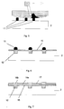
- a typical semiconductor device 1 is shown in top-view in Fig 1, which may be a photovoltaic cell, sometimes called a solar cell.
- a semiconductor substrate 2 of a first doping type has doped surface regions 5, typically of a second doping type, and a metallisation pattern 3 on at least one major surface.
- the metallisation pattern 3 usually includes elongate metal electrodes 4 between and under which are doped regions 5, e.g. emitter, collector or gate regions.
- the electrodes 4 may form ohmic contacts to heavily doped regions 6 (shown best in Figs. 3 and 4) of the underlying substrate 2. Electrodes 4 collect from, or supply electric currents to the regions 5, which may include semiconductor devices.
- region 5 is usually the emitter region.
- Solar cells generally suffer from losses in the emitter region 5.
- the doping level in the emitter region 5 should be at a low level for optimised photon collection and conversion whereas the regions 6 should be doped strongly and deeply doped to give good ohmic contact to the metallisation pattern 4 without shunting the buried junction 8 (see Figs. 2, 3).
- Total system cost may be optimised by selecting the best combination of low manufacturing cost with device losses.
- a typical homogenous emitter/collector process sequence usually incorporates a structuring and chemical preparation of the wafer surfaces, a diffusion step (in-diffusion of a dopant from the surface/s), an optional oxide passivation step, an optional anti-reflective coating step (e.g. TiO 2 or Si 3 N 4 ) which may provide additional passivation and a metallisation sequence (preferably by screen printing).
- a structuring and chemical preparation of the wafer surfaces usually incorporates a structuring and chemical preparation of the wafer surfaces, a diffusion step (in-diffusion of a dopant from the surface/s), an optional oxide passivation step, an optional anti-reflective coating step (e.g. TiO 2 or Si 3 N 4 ) which may provide additional passivation and a metallisation sequence (preferably by screen printing).
- FIG. 3 An improvement is shown in Fig. 3 in which the regions 5 are etched to a depth such that the selective emitter/collector regions are formed.
- the depth of the doped layer between the emitter/collector fingers 4 is reduced and hence, the doping level is reduced.
- Such devices are described in the article "Simple integral screenprinting process for selective emitter polycrystalline silicon solar cells", by Szlufcik et al., Appl. Phys. Lett. Vol. 59, Issue 13, pp 1583 - 1584, 1991 and in DE 44 01 782 in which the diffusion areas between the emitters are partially etched after the metal contacts have been protected by a protection layer.
- Application of the protection layer typically a polymer paste requires an extra masking step. This latter technique has the disadvantages of an extra masking and a difficult etching step which increase the complexity and cost of manufacture.
- Fig. 4 shows schematically in cross-section the more effective solution of a selective emitter/collector which has deep emitter/collector doping profile regions 6 with a high dopant surface concentration under the front metal contacts 3 and a shallow doping profile that is optimised for carrier collection in adjacent areas 5.
- the selective emitter/collector structure requires a more complicated manufacturing process as described, for instance, in DE 42 17 428 in which a shallow emitter layer is diffused over the whole front surface of the substrate followed by the formation of passivation/oxide layers. Openings are then formed in the oxide layers using a laser beam and the oxide layers used as a mask for a deep diffusion step of the emitter contact areas.
- the metal contacts 3, 4 are then formed in the trenches opened by the laser.
- the method of manufacture according to the present invention is specified in claim 1.
- the semiconductor device in accordance with the present invention is specified in claim 10.
- the present invention applies primarily to the formation of two different, selectively diffused regions on semiconductor substrates with different doping levels.
- the advantageous design of a selective emitter or collector structure is realised without any additional process step or complication of the process in comparison with homogeneous emitter/collector structures.
- the most favourable process sequence makes use of screen printing a solids based dopant paste to form the diffusion regions by a first high temperature heat treatment step and screen printing a metal paste to provide the metallisation by a second high temperature heat treatment step.
- the selective emitter or collector process in accordance with the present invention may have the same number of process steps as a typical homogenous emitter/collector process and less steps than for a conventional selective emitter/collector process.
- the method of the present invention provides a simple and economical manufacturing method for photovoltaic devices which have advantageous results over known homogeneous emitter/collector structures. Less dopant source material is required as compared with the homogeneous emitter/collector process, thus reducing the production cost while improving the final cell performance.
- the present invention is a simplification of known selective emitter or collector formation process sequences.
- the selective emitter or collector structure in accordance with the present invention is formed within only one diffusion step. No additional masking and/or etching process steps are needed to form the selective emitter or collector.
- the methods of the present invention may be applied to the formation of differentiated p-type regions in an n-type substrate or the formation of n++-and n+-type regions in an undoped or n-type substrate or p++- and p+-type regions in an undoped or p-type substrate. Further, the invention will mainly be described with reference to a monofacial solar cell but the invention may be applied equally well to a bifacial solar cell.
- the use of the simple process in accordance with the present invention to form for instance an emitter or a collector with differently doped regions with only one high temperature step and without using etching or masking techniques is not limited to solar cells.
- the technique can be used in other micro-electronic production processes as long as there are similar tolerances in the lateral size of doped regions and metal contacts and the diffusion profiles.
- Photodetectors and microengineered sensors of all types, heat conversion semiconductor devices as well as semiconductor devices of all types such as thyristors are other devices where a reduction of the production cost may be achieved by using the method in accordance with the present invention.
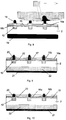
- Figs. 5 to 10 show schematically a selective emitter or collector manufacturing process in accordance with the present invention as applied to a solar cell 1.
- the processing may start with an as-cut semiconductor substrate 2.
- the substrate 2 may be single crystalline, polycrystalline or amorphous silicon.
- the quality of the substrate may be less than required for transistor devices, for instance solar grade silicon as disclosed in "Solar cells” 1992, by Martin Green, University of New South Wales. No limits are expected with respect to the size of substrate 2, and the size will depend upon commercially available materials.
- 10 cm x 10 cm silicon substrates with a thickness of 200 to 400 micron are used but the invention is not limited thereto.
- the substrate 2 in accordance with the present invention is preferably silicon but the invention is not limited thereto.
- the substrate 2 may be GaAs or any other similar semiconductor substrate 2 which requires adjacent diffused doped regions with a selective difference in doping levels.
- the semiconductor substrate 2 is chemically cleaned and the substrate 2 is subsequently etched to remove the saw damage from the surface, for instance with a 40% by weight of NaOH in deionised water (DI water) solution at 80 °C for 2 - 4 minutes.
- DI water deionised water
- the substrate may then be rinsed in DI water up to 8 MOhmcm.
- a texture e.g. pyramidal structures, may be provided mechanically or chemically on one or both major surfaces of the substrate 2 as described for instance in the article "Texturization methods for multicrystalline silicon solar cells", by Willeke and Fath, Proc. 13th European Photovoltaic Solar Energy Conf. and Exhibition, France, 23-27 Oct. 1995.
- a suitable etch for this purpose includes a solution of 1.3 wt % NaOH and 5% isopropyl alcohol by volume in DI water at 90 °C for 10 minutes. After etching the substrate 2 is chemically cleaned and rinsed in DI water as before. In the drawings the texturizing has been omitted for clarity reasons.
- heavily doped deep diffusion regions 12 are to be formed under the front surface metal contact regions 20 (Figs. 8 and 9) and a shallow weakly doped emitter or collector region 15 is to be formed elsewhere (Fig. 6).
- a solids based dopant source 11 containing a suitable dopant in the form of a paste or similar is selectively applied at least to one major surface of substrate 2 in a defined pattern which may take the form of lines and/or areas.
- the paste 11 is selectively applied to those regions of the substrate surface where deep diffusion regions 12 are to be formed in a later step.
- Various techniques may be used to apply the dopant paste 11 selectively to the substrate 2.
- the dopant paste 11 is preferably carried out in a very defined and reproducible way.
- Preferred techniques have good repeatability such as screen printing, offset, gravure, ink jet printing or paste writing.
- the paste 11 is preferably printed onto the substrate by thick film techniques such as screen printing in order to give good repeatability in a high volume production process.
- As the front surface metallisation pattern 20 (Figs. 8 and 9) has to be applied later to the substrate 2 in alignment with the deep regions 12 where the dopant paste 11 was applied previously, it is quite advantageous to use the same technique for applying both dopant paste 11 and front side metal paste 18.
- the good repeatability of screen printing allows subsequent application of a metal paste 18 to form a front surface metallisation pattern 20 (Fig. 8) using the same technique and using the same type of screens as used for applying paste 11 (Fig. 5).
- a DEK model 1760RS screen printer may be used to apply the paste 11.
- Pastes 11 containing dopant sources such as P, B, As, etc. can be used depending on the conductivity type and chemical nature of substrate 2.
- the paste may be a phosphorous containing paste 11 as described in EP- 0 108 065 or a commercially available paste such as P101 from Soltech NV, Belgium.
- the paste 11 may contain boron.
- the preferred low cost solar cell manufacturing process in accordance with the present invention utilises a p-type crystalline Si substrate 2 and phosphorous as a dopant source to form an n-type emitter 12, 15 on the front side.
- the viscosity of the paste 11 should be selected so that it may be applied accurately by the appropriate technique, e.g. screen printing, but does not flow or spread significantly on the substrate 2.
- the paste 11 is preferably thixotropic.
- the viscosity of the dopant paste 11 is preferably high enough to prevent significant lateral flow before or during drying or during the heat treatment step that would lead to significantly wider lines or areas of applied dopant paste 11 than the width of the front surface metal contacts 20 applied later. However, a small lateral widening of the lines or areas of paste 11 beyond the intended lines or areas which will subsequently be covered by the metal contacts 20 may be desirable to avoid shunting the junction 8 with the metal contacts 20.
- the application of the subsequent metal contacts 20 is performed to within a certain tolerance and it is preferable if the paste lines and areas 11 are slightly larger than the subsequent metal contact areas and lines 20 so that the alignment of the metal paste lines and areas 18 with the deep doped regions 12 may be carried out repeatably and accurately.
- the paste 11 is dried immediately after application.
- the patterned substrate 2 is preferably loaded as quickly as possible into a drying oven in which the viscous paste 11 is dried at temperatures between 150 - 350 °C, preferably between 150 and 200 °C, for about 1 to 10 minutes to fix its position on the substrate 2.
- a Tempress conveyor belt dryer a DEK infrared belt dryer or similar may be used.
- the substrate 2 is preferably subjected to a two phase heat treatment step.
- the substrate 2 with the dried paste is loaded directly into a diffusion oven such as a Tempress/Lindberg conveyor belt diffusion furnace, e.g. from Gemco in the Netherlands.
- a diffusion oven such as a Tempress/Lindberg conveyor belt diffusion furnace, e.g. from Gemco in the Netherlands.
- the temperature is raised at about 100 - 150 °C per minute up to a about 600 °C and the remaining organic components from the dopant paste 11 are burned out, preferably in an air or oxygen atmosphere.
- the dopant is driven at high temperature from the paste 11 directly into the substrate 2.
- This second heat treatment phase is preferably carried out in an inert gas atmosphere.
- a deep doped region 12 is formed in this high temperature step as shown schematically in Fig. 6, in which the dopant from the dopant paste 11 is diffused directly into the substrate 2 immediately below the paste areas and lines 11.
- a shallow region 15 is formed by indirect diffusion from the dopant 11 into the surrounding atmosphere and from there into the exposed areas of the substrate 2.
- the patterned substrate 2 is placed on a horizontal movable belt in a continuous oven, for example a Tempress/Lindberg conveyor belt diffusion furnace mentioned above, and maintained in an inert gas atmosphere such as nitrogen.
- the temperature is raised to 800 to 1100 °C, preferably 900 to 950°C, while keeping a temperature gradient at about 150°C/minute.
- the substrate 2 is preferably maintained at this temperature for about 10 to 60 minutes.
- the indirect diffusion forms second diffusion regions 15 at places neighbouring the regions where the dopant paste 11 is applied. As shown schematically in Fig. 11, the dopant atoms start to diffuse out of the paste 11 in all directions. Thus the underlying semiconductor substrate 2 experiences a relatively strong in-diffusion of dopant atoms at the regions 12 where the paste 11 is in direct contact with it as compared to the other regions of the substrate surface. The dopant diffuses from the ambient atmosphere into the substrate 2 at those places where no dopant paste 11 was selectively applied.
- the indirect doping may produce a second diffusion layer 15 in the substrate 2 having a lower concentration than that of the first diffusion regions 12 of the substrate 2 immediately below where the paste 11 was applied.
- the low concentration of dopant atoms in the atmosphere surrounding the substrate 2 during the high temperature step may also lead to shallower second diffusion regions 15 compared with the first diffusion regions 12.
- the concentration of dopant atoms in the surrounding gas atmosphere can be much lower than in the paste 11 itself and consequently the diffusion rate is much lower. This results in a relatively deeply doped region 12 where the dopant source 11 is in contact with the substrate 2 and in weaker and shallower doped regions 15 at the substrate-gas interface.
- the differences in the two diffusion regions can be selectively controlled by changing the dopant paste composition, the atmosphere, the diffusion time or the diffusion temperature.
- the conditions may be optimised to produce a shallow second diffusion region 15 while the first diffusion region 12 should be just deep enough to allow formation of good ohmic front surface metal contacts 20 without shunting the junction 8. It is also possible to execute the diffusion sequence using a gaseous dopant atmosphere, as for instance POCl 3 , BBr3 etc. in a closed tube furnace. By adjusting the relative amount of direct diffusion from the gaseous dopant gas and indirect diffusion from the dopant paste 11 to the second diffusion region 15 it is possible to manipulate the diffusion profiles of the first and second diffusion regions 12, 15 selectively and independently. Further, more than one paste 11 may be used to form selectively, by heat treatment, different regions in the substrate 2.
- a gaseous dopant atmosphere as for instance POCl 3 , BBr3 etc.
- the different pastes 11 may have different concentrations of dopant atoms or may contain different types of dopant. Further, some of the paste 11 may contain no dopant atoms and may be merely used as a mask to prevent indirect doping of the underlying layer of the substrate 2.
- the semiconductor device 1 is a photovoltaic cell
- variations in the depth or dopant concentration of the deep first diffusion regions 12 which form part of the emitter or collector regions may not influence the cell performance strongly whereas variations in the shallow second diffusion regions 15 may have a much bigger impact on cell characteristics.
- the second diffusion region 15 normally has a much lower surface dopant concentration and depth than the deep regions 12.
- the doping conditions for the second diffusion region 15 are preferably optimised for carrier collection. Carrier collection is sensitive to dopant concentration and depth.
- the diffusion in the first diffusion region 12 at those places where the diffusion paste 12 has been applied and where the metallisation pattern 18 will be printed later in the process sequence, has to be only deep enough and have a high enough surface dopant concentration so that good ohmic contacts 20 can be formed with the emitter or collector region 12 without shunting the junction 8.
- differentiated deep and shallow doped regions 12, 15 may be produced in a single doping step.
- Surface dopant concentrations may be, for example, in the range typically above 10 20 phosphorus atoms/cm 3 for the deeper doped regions 12 and in the range 5 x 10 18 to 10 20 , typically 1 x 10 19 to 5 x 10 19 phosphorus atoms/cm 3 for the shallower doped regions 15.
- Junction depths for the deeper doped regions 12 are preferably at least 0.3 micron, more preferably at least 0.5 micron and typically 0.6 micron and for the shallower doped regions 15 up to 0.3 micron, typically 0.2 micron.
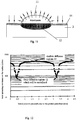
- FIG. 12 shows a lateral spreading resistance scan of a selective emitter or collector structure produced for a solar cell in accordance with the present invention carried out in accordance with the article "Spreading resistance measurements - An overview", by J. R. Ehrstein, D. C. Gupta, and P. H. Langer, Emerging Semiconductor Technology, ASTM STP 960, Am. Soc. for Test. and Mat. 1986. Paste lines 11 of a width of 100 micron were spaced at a distance of about 3 mm from each other.
- the selective emitter or collector structure has low resistance, deeply and strongly diffused regions 12 where the metallisation 20 has to be applied and shallow and weak diffusion regions 15 in the emitter or collector region where photons are absorbed and create carriers. As can be seen from Fig.
- the paste has resulted in low resistance regions 12 over a narrow distance about the size of their own width.
- the resistance descreases monotonically towards the shallow regions 15 over a distance of about 1mm.
- the resistance ratio of the deep and shallow regions 12, 15 is above 5 and is about 10 or more for a solar cell. This is caused by a similar variation in the dopant atom concentration in these areas.
- the deeply diffused regions 12 and the shallow diffused regions 15 would alternate periodically showing a steep gradient at the transition regions where there is roughly one order of magnitude difference in the surface concentration of dopant atoms The higher the dopant concentration the lower the electrical resistance.
- the monotonic decrease in dopant concentration and associated electrical resistance from the weakly doped regions 15 towards the deeply diffused regions 12 where the metal contacts 20 will be placed in a finished solar cell provides excellent carrier collection properties.
- the increasing gradient in the surface concentration of dopant atoms towards the regions where the metal contacts will be placed in the finished solar cell facilitates the carrier transport towards these collecting contacts 20.
- a monotonic increase of dopant atom density may be obtained in the surface region of the substrate 2 between the shallow regions 15 and the deep regions 12 with at least a fivefold, and typically an order of magnitude or more, difference between the dopant density in the shallow regions 15 and the dopant density in the deep regions 12.
- the remaining diffusion glass on the silicon substrate surface may be removed in an chemical etching solution of about 25%-50% HF in DI water and the substrate 2 is cleaned and rinsed afterwards.
- the present invention includes that the diffusion glass is optionally not removed and the process continues to an oxidation/passivation step. This may avoid an HF acid cleaning step which is an advantage environmentally.
- the diffusion sequence may be followed by an optional oxidation step where an SiO 2 layer 16a and 16b is formed on the surfaces of the substrate by exposing the substrates to an O 2 atmosphere, typically in a quartz boat, for 1 - 20 minutes at temperatures ranging from 800 - 950 degree C.
- This SiO 2 layer 16a, 16b serves to passivate defects in the surface emitter/collector region 15 of the substrate 2 which could decrease the solar cell performance. Passivation using an oxide layer reduces the surface recombination velocity which reduces the loss of carriers, hence improving efficiency.
- a passivating layer 16a, 16b such as an oxide may be applied but also an anti-reflection coating layer (ARC) 17.
- the ARC layer 17 may be applied by chemical vapour deposition (CVD, e.g. a TiO 2 layer) or plasma enhanced CVD (PECVD, e.g. a silicon nitride layer) or similar techniques.
- CVD chemical vapour deposition
- PECVD plasma enhanced CVD
- the metallisation sequence comprises usually two or three contact printing steps: front contact 20 and one or two back contact patterns 21 depending on how many different metals are used.
- metal paste 18 is selectively applied to the front side of the substrate 2 in alignment with regions 12 that are heavily doped.
- a further metal paste 19 is applied either selectively or non-selectively to the backside of the substrate 2.
- Screen printing and subsequent drying is the most preferred way to apply these contacts, however other thick film techniques mentioned above or evaporation may be used instead.
- Each printing step is followed by a drying step at moderate temperatures around 250 degree C, e.g. by infra-red heaters. As shown in Fig.
- the metal pastes 18, 19 are then sintered at high temperatures ranging from 650 to 900 degree C for typically about 30 to 200 seconds to form good ohmic contacts 20 on the front side of the substrate 2 without shunting the junction 8, as well as good ohmic contacts 21 on the back side of substrate 2.
- the contacts 20 and 21 are formed through any ARC or oxide layer 16b; 17.
- the peak temperature and temperature profile are very important and have to be adapted for each metallisation paste and process sequence separately.
- the front side and back side contacts screen-printed with metal paste 18, 19 are both sintered together in one high temperature step after having been dried separately.
- a back surface field (BSF) layer 22 is formed at the same time on the back side of substrate 2 as shown schematically in Fig. 9.
- BSF 22 back surface field
- an anti-reflection coating (ARC) layer 23 can be applied after metallisation rather than the ARC layer 17 applied before metallisation and described with reference to Fig. 8.
- Typical ARC layers may include TiO2, Si 3 N 4 , or Ta 2 O 5 , or similar materials and can be applied by various techniques.
- Metal contact sintering temperatures as high as 800 °C can be used for the contact formation without shunting the junction 8. Where aluminium is used for the metal contacts, sintering at such high temperatures has additional advantages as for instance Al gettering and BSF formation.
- Thick film techniques for applying the metal and/or doping pastes such as screen printing show an excellent repeatability.
- the substrates 2 may be loaded each time by the screen printer into the same position under the screen by means of a CCD camera controlled positioning system. Alignment of metallisation and diffusion patterns can be controlled if oxide and/or ARC layers 16a, 16b; 17, 23 have been applied by utilising the different colour of the slightly wider first diffusion regions 12 under the microscope. With deposition of an ARC layer 17, 23, the substrate 2 shows a different colour at those places where the substrate has higher dopant surface concentrations. This is because the underlying oxide layer 16b grows thicker at places with higher dopant surface concentration compared with the oxide layer 16a over the areas 15 of lower doping level.
- the anti-reflective coating (ARC) layer 17 or 23 As long as the anti-reflective coating (ARC) layer 17 or 23 is applied, the underlying pattern will be visible. The reason for this is a faster oxidation at places with higher dopant surface concentration, resulting in a thicker oxide layer 16. After applying an ARC layer 17 or 23 this difference in oxide thickness becomes visible as a difference in optical thickness and therefor colour of the layers 16b + 17 or 23 compared to 16a + 17 or 23.
- ARC anti-reflective coating
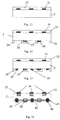
- Figs. 13 to 16 show schematically the manufacturing steps of a semiconductor device 30 in accordance with a further embodiment of the present invention. As one embodiment of the present invention has been described in some detail with reference to Figs. 5 to 10, the description of the further embodiment will not be made in detail. The formation of passivation layers, cleaning steps and other details of the process other than the main doping steps will not be described. The process of the further embodiment is suitable for forming a photovoltaic device.
- a first doped paste pattern 31 is applied selectively to a semiconductor substrate 2 which may be a silicon substrate and may be undoped or may be p-type or n-type conductivity.
- the paste 31 may be applied by any of the thick-film techniques described previously.
- the paste pattern 31 is then dried.
- the first dopant paste 31 may have either the first or second conductivity.
- the first paste pattern 31 is optionally protected by applying a layer of another material, e.g. a further paste 32.
- Paste 32 may have a different concentration or type compared with paste 31 or may be undoped.
- Paste 32 may be applied over a major surface of substrate 2.
- the paste layer 32 is then dried.
- a third paste pattern 33 is optionally applied selectively to a further major surface of the substrate 2.
- Paste pattern in then dried.
- Paste 33 may have either the first or second conductivity.
- Paste pattern 33 and other selected parts of the surface of substrate 2 may be protected by the selective application of an undoped material 34, which may be a paste.
- the paste 34 may be applied by any of the thick-film techniques mentioned above. Paste pattern 34 is then dried.
- Paste 35 may be applied selectively to a major surface of the substrate 2.
- Paste 35 may include dopant of either conductivity type.
- Paste 35 may be applied by any of the thick-film techniques mentioned above.
- Paste pattern 35 is then dried.
- the patterned substrate 2 is then placed in a furnace and the dopants from those pastescontaining dopant atoms, e.g. 31, 33, 35, are driven into the substrate 2 to form doped layers 37, 39 and 41, respectively.
- the dopant atoms from the non-protected pastes diffuse indirectly into regions 42 of the substrate which are not protected to form shallow weakly doped regions 42.
- metal pastes are applied in alignment with the regions 37, 39 and optionally 41 and sintered at high temperature to form metal contacts 36, 38, and optionally 40, respectively.
- substrate 2 may be p-type silicon
- pastes 31, 35 and optionally 32 may be phosphorous containing pastes
- paste 33 may be a boron paste
- paste 34 may be undoped.
- Paste 32 may be omitted.
- the device produced with a single diffusion step in accordance with the further embodiment of the present invention may be a solar cell having a selective emitter on the top side and a floating junction on the back side. Such a photovoltaic device may show a better cell performance than a monofacial cell with a conventional back side metallisation over the whole back surface.
- the device produced by the method of the further embodiment may be used in addition as a bifacial solar cell.
- the process in accordance with the further embodiment has the advantage that solar cells can be produced having improved efficiency values and short circuit currents resulting from a more ideal emitter/collector structure and a more ideal back contact.
- the back contact in accordance with the further embodiment does not have metallisation over the whole of the back major surface of the substrate 2 resulting in better back surface reflection or to its use in bifacial cells designs.
Abstract
The present invention describes a method of manufacturing a semiconductor device,
comprising a semiconducting substrate (2) in the shape of a slice, the method comprising
the steps of:
The semiconductor device in accordance with the present invention made by the above
method may have a monotonically decreasing resistance value between the first and
second diffusion regions (12, 15).
Description
The present invention relates to a semiconducting device and a method for the
manufacture thereof, in particular to a photovoltaic cell having two selectively diffused
regions produced in a single diffusion step.
Many semiconductor devices make use of differently doped regions of the same
conductivity type (p or n) to achieve better performance of the device. The formation of
these differently doped regions often implies additional process steps that increase the cost
of production. A typical semiconductor device 1 is shown in top-view in Fig 1, which
may be a photovoltaic cell, sometimes called a solar cell. A semiconductor substrate 2 of a
first doping type has doped surface regions 5, typically of a second doping type, and a
metallisation pattern 3 on at least one major surface. The metallisation pattern 3 usually
includes elongate metal electrodes 4 between and under which are doped regions 5, e.g.
emitter, collector or gate regions. The electrodes 4 may form ohmic contacts to heavily
doped regions 6 (shown best in Figs. 3 and 4) of the underlying substrate 2. Electrodes 4
collect from, or supply electric currents to the regions 5, which may include
semiconductor devices. For a solar cell, region 5 is usually the emitter region.
Solar cells generally suffer from losses in the emitter region 5. For optimum
performance the doping level in the emitter region 5 should be at a low level for optimised
photon collection and conversion whereas the regions 6 should be doped strongly and
deeply doped to give good ohmic contact to the metallisation pattern 4 without shunting
the buried junction 8 (see Figs. 2, 3). Total system cost may be optimised by selecting the
best combination of low manufacturing cost with device losses.
A homogenous emitter/collector design for a solar cell as shown schematically in
cross-section in Fig. 2 having front metal contacts 4 back metal contacts 9, a diffusion
region 7 and a junction 8. The same diffusion region 7 over the whole front side
combined with a low-cost metallisation technique such as screen printing of front metal
contacts 4 leads to considerable efficiency losses. This is because the diffusion profile of
diffusion region 7 (dopant surface concentration and emitter/collector depth from the
surface to the junction 8) required to form good ohmic contacts with this metallisation
technique is not ideal for the conversion of light to electrical energy in the intermediate
emitter/collector regions 5.
A typical homogenous emitter/collector process sequence usually incorporates a
structuring and chemical preparation of the wafer surfaces, a diffusion step (in-diffusion of
a dopant from the surface/s), an optional oxide passivation step, an optional anti-reflective
coating step (e.g. TiO2 or Si3N4) which may provide additional passivation and a
metallisation sequence (preferably by screen printing).
An improvement is shown in Fig. 3 in which the regions 5 are etched to a depth
such that the selective emitter/collector regions are formed. The depth of the doped layer
between the emitter/collector fingers 4 is reduced and hence, the doping level is reduced.
Such devices are described in the article "Simple integral screenprinting process for
selective emitter polycrystalline silicon solar cells", by Szlufcik et al., Appl. Phys. Lett.
Vol. 59, Issue 13, pp 1583 - 1584, 1991 and in DE 44 01 782 in which the diffusion areas
between the emitters are partially etched after the metal contacts have been protected by a
protection layer. Application of the protection layer, typically a polymer paste requires an
extra masking step. This latter technique has the disadvantages of an extra masking and a
difficult etching step which increase the complexity and cost of manufacture.
Fig. 4 shows schematically in cross-section the more effective solution of a
selective emitter/collector which has deep emitter/collector doping profile regions 6 with a
high dopant surface concentration under the front metal contacts 3 and a shallow doping
profile that is optimised for carrier collection in adjacent areas 5. However, the selective
emitter/collector structure requires a more complicated manufacturing process as
described, for instance, in DE 42 17 428 in which a shallow emitter layer is diffused over
the whole front surface of the substrate followed by the formation of passivation/oxide
layers. Openings are then formed in the oxide layers using a laser beam and the oxide
layers used as a mask for a deep diffusion step of the emitter contact areas. The metal
contacts 3, 4 are then formed in the trenches opened by the laser.
Known manufacturing methods of a selective emitter/collector using low cost
metallisation techniques such as screen printing require a second diffusion step and/or
masking and/or etching steps resulting in the need for alignment of the metallisation
pattern 3 with the higher doped regions 6 on the front side of the semiconductor device 1.
General methods of making photovoltaic devices are described in "Physics,
technology and use of Photovoltaics" by R. J. Overstraeten and R. P. Mertens, Adam
Higler Ltd., 1986 which is incorporated herein by reference.
The method of manufacture according to the present invention is specified in claim
1. The semiconductor device in accordance with the present invention is specified in
claim 10.
The present invention applies primarily to the formation of two different,
selectively diffused regions on semiconductor substrates with different doping levels. The
advantageous design of a selective emitter or collector structure is realised without any
additional process step or complication of the process in comparison with homogeneous
emitter/collector structures. The most favourable process sequence makes use of screen
printing a solids based dopant paste to form the diffusion regions by a first high
temperature heat treatment step and screen printing a metal paste to provide the
metallisation by a second high temperature heat treatment step.
The selective emitter or collector process in accordance with the present
invention, for example for a photovoltaic device, may have the same number of process
steps as a typical homogenous emitter/collector process and less steps than for a
conventional selective emitter/collector process. The method of the present invention
provides a simple and economical manufacturing method for photovoltaic devices which
have advantageous results over known homogeneous emitter/collector structures. Less
dopant source material is required as compared with the homogeneous emitter/collector
process, thus reducing the production cost while improving the final cell performance.
The present invention is a simplification of known selective emitter or collector
formation process sequences. The selective emitter or collector structure in accordance
with the present invention is formed within only one diffusion step. No additional masking
and/or etching process steps are needed to form the selective emitter or collector.
In the following the invention will be described with reference to certain specific
embodiments and with reference to the drawings but the invention is not limited thereto
but only by the claims. In the drawings some of the dimensions, for instance the thickness
of layers, may have been exaggerated for purposes of clarity. In particular, the invention
will be explained with reference to a photovoltaic device, sometimes called a solar cell,
but the invention is not limited thereto but may find application in semiconductor devices
generally. Further, the invention will mainly be described with reference to the formation
of differentiated n++- and n+-type regions in a p-type substrate. The invention is not
limited thereto. The methods of the present invention may be applied to the formation of
differentiated p-type regions in an n-type substrate or the formation of n++-and n+-type
regions in an undoped or n-type substrate or p++- and p+-type regions in an undoped or
p-type substrate. Further, the invention will mainly be described with reference to a
monofacial solar cell but the invention may be applied equally well to a bifacial solar cell.
The use of the simple process in accordance with the present invention to form for
instance an emitter or a collector with differently doped regions with only one high
temperature step and without using etching or masking techniques is not limited to solar
cells. The technique can be used in other micro-electronic production processes as long as
there are similar tolerances in the lateral size of doped regions and metal contacts and the
diffusion profiles. Photodetectors and microengineered sensors of all types, heat
conversion semiconductor devices as well as semiconductor devices of all types such as
thyristors are other devices where a reduction of the production cost may be achieved by
using the method in accordance with the present invention.
Figs. 5 to 10 show schematically a selective emitter or collector manufacturing
process in accordance with the present invention as applied to a solar cell 1. In a low-cost
production process in accordance with the present invention, the processing may start
with an as-cut semiconductor substrate 2. The substrate 2 may be single crystalline,
polycrystalline or amorphous silicon. The quality of the substrate may be less than
required for transistor devices, for instance solar grade silicon as disclosed in "Solar cells"
1992, by Martin Green, University of New South Wales. No limits are expected with
respect to the size of substrate 2, and the size will depend upon commercially available
materials. At the present time 10 cm x 10 cm silicon substrates with a thickness of 200 to
400 micron are used but the invention is not limited thereto. The substrate 2 in accordance
with the present invention is preferably silicon but the invention is not limited thereto. The
substrate 2 may be GaAs or any other similar semiconductor substrate 2 which requires
adjacent diffused doped regions with a selective difference in doping levels.
Initially the semiconductor substrate 2 is chemically cleaned and the substrate 2 is
subsequently etched to remove the saw damage from the surface, for instance with a 40%
by weight of NaOH in deionised water (DI water) solution at 80 °C for 2 - 4 minutes. The
substrate may then be rinsed in DI water up to 8 MOhmcm. Optionally, a texture, e.g.
pyramidal structures, may be provided mechanically or chemically on one or both major
surfaces of the substrate 2 as described for instance in the article "Texturization methods
for multicrystalline silicon solar cells", by Willeke and Fath, Proc. 13th European
Photovoltaic Solar Energy Conf. and Exhibition, France, 23-27 Oct. 1995. For example, a
suitable etch for this purpose includes a solution of 1.3 wt % NaOH and 5% isopropyl
alcohol by volume in DI water at 90 °C for 10 minutes. After etching the substrate 2 is
chemically cleaned and rinsed in DI water as before. In the drawings the texturizing has
been omitted for clarity reasons.
In accordance with the present invention, heavily doped deep diffusion regions 12
are to be formed under the front surface metal contact regions 20 (Figs. 8 and 9) and a
shallow weakly doped emitter or collector region 15 is to be formed elsewhere (Fig. 6).
As shown schematically in Fig. 5, a solids based dopant source 11 containing a suitable
dopant in the form of a paste or similar is selectively applied at least to one major surface
of substrate 2 in a defined pattern which may take the form of lines and/or areas. The
paste 11 is selectively applied to those regions of the substrate surface where deep
diffusion regions 12 are to be formed in a later step. Various techniques may be used to
apply the dopant paste 11 selectively to the substrate 2. Application of the dopant paste
11 is preferably carried out in a very defined and reproducible way. Preferred techniques
have good repeatability such as screen printing, offset, gravure, ink jet printing or paste
writing. The paste 11 is preferably printed onto the substrate by thick film techniques such
as screen printing in order to give good repeatability in a high volume production process.
As the front surface metallisation pattern 20 (Figs. 8 and 9) has to be applied later to the
substrate 2 in alignment with the deep regions 12 where the dopant paste 11 was applied
previously, it is quite advantageous to use the same technique for applying both dopant
paste 11 and front side metal paste 18. The good repeatability of screen printing allows
subsequent application of a metal paste 18 to form a front surface metallisation pattern 20
(Fig. 8) using the same technique and using the same type of screens as used for applying
paste 11 (Fig. 5). A DEK model 1760RS screen printer may be used to apply the paste 11.
The viscosity of the paste 11 should be selected so that it may be applied
accurately by the appropriate technique, e.g. screen printing, but does not flow or spread
significantly on the substrate 2. The paste 11 is preferably thixotropic. The viscosity of the
dopant paste 11 is preferably high enough to prevent significant lateral flow before or
during drying or during the heat treatment step that would lead to significantly wider lines
or areas of applied dopant paste 11 than the width of the front surface metal contacts 20
applied later. However, a small lateral widening of the lines or areas of paste 11 beyond
the intended lines or areas which will subsequently be covered by the metal contacts 20
may be desirable to avoid shunting the junction 8 with the metal contacts 20. The
application of the subsequent metal contacts 20 is performed to within a certain tolerance
and it is preferable if the paste lines and areas 11 are slightly larger than the subsequent
metal contact areas and lines 20 so that the alignment of the metal paste lines and areas 18
with the deep doped regions 12 may be carried out repeatably and accurately.
Preferably, the paste 11 is dried immediately after application. The patterned
substrate 2 is preferably loaded as quickly as possible into a drying oven in which the
viscous paste 11 is dried at temperatures between 150 - 350 °C, preferably between 150
and 200 °C, for about 1 to 10 minutes to fix its position on the substrate 2. For drying a
Tempress conveyor belt dryer, a DEK infrared belt dryer or similar may be used. After
drying the paste the substrate 2 is preferably subjected to a two phase heat treatment step.
The substrate 2 with the dried paste is loaded directly into a diffusion oven such as a
Tempress/Lindberg conveyor belt diffusion furnace, e.g. from Gemco in the Netherlands.
In a first phase the temperature is raised at about 100 - 150 °C per minute up to a about
600 °C and the remaining organic components from the dopant paste 11 are burned out,
preferably in an air or oxygen atmosphere.
In a second phase, the dopant is driven at high temperature from the paste 11
directly into the substrate 2. This second heat treatment phase is preferably carried out in
an inert gas atmosphere. A deep doped region 12 is formed in this high temperature step
as shown schematically in Fig. 6, in which the dopant from the dopant paste 11 is diffused
directly into the substrate 2 immediately below the paste areas and lines 11. At the same
time, a shallow region 15 is formed by indirect diffusion from the dopant 11 into the
surrounding atmosphere and from there into the exposed areas of the substrate 2.
Preferably, the patterned substrate 2 is placed on a horizontal movable belt in a
continuous oven, for example a Tempress/Lindberg conveyor belt diffusion furnace
mentioned above, and maintained in an inert gas atmosphere such as nitrogen. The
temperature is raised to 800 to 1100 °C, preferably 900 to 950°C, while keeping a
temperature gradient at about 150°C/minute. The substrate 2 is preferably maintained at
this temperature for about 10 to 60 minutes. There is not only an in-diffusion of the
dopant from the paste 11 into the substrate 2 at the places where the paste 11 is in
intimate contact with the substrate 2 but there is also an out-diffusion of the dopant into
the surrounding atmosphere from where the dopant atoms can re-enter the substrate 2
indirectly. The indirect diffusion forms second diffusion regions 15 at places neighbouring
the regions where the dopant paste 11 is applied. As shown schematically in Fig. 11, the
dopant atoms start to diffuse out of the paste 11 in all directions. Thus the underlying
semiconductor substrate 2 experiences a relatively strong in-diffusion of dopant atoms at
the regions 12 where the paste 11 is in direct contact with it as compared to the other
regions of the substrate surface. The dopant diffuses from the ambient atmosphere into the
substrate 2 at those places where no dopant paste 11 was selectively applied. The indirect
doping may produce a second diffusion layer 15 in the substrate 2 having a lower
concentration than that of the first diffusion regions 12 of the substrate 2 immediately
below where the paste 11 was applied. The low concentration of dopant atoms in the
atmosphere surrounding the substrate 2 during the high temperature step may also lead to
shallower second diffusion regions 15 compared with the first diffusion regions 12. The
concentration of dopant atoms in the surrounding gas atmosphere can be much lower
than in the paste 11 itself and consequently the diffusion rate is much lower. This results in
a relatively deeply doped region 12 where the dopant source 11 is in contact with the
substrate 2 and in weaker and shallower doped regions 15 at the substrate-gas interface.
The differences in the two diffusion regions can be selectively controlled by changing the
dopant paste composition, the atmosphere, the diffusion time or the diffusion temperature.
The conditions may be optimised to produce a shallow second diffusion region 15 while
the first diffusion region 12 should be just deep enough to allow formation of good ohmic
front surface metal contacts 20 without shunting the junction 8. It is also possible to
execute the diffusion sequence using a gaseous dopant atmosphere, as for instance POCl3,
BBr3 etc. in a closed tube furnace. By adjusting the relative amount of direct diffusion
from the gaseous dopant gas and indirect diffusion from the dopant paste 11 to the second
diffusion region 15 it is possible to manipulate the diffusion profiles of the first and second
diffusion regions 12, 15 selectively and independently. Further, more than one paste 11
may be used to form selectively, by heat treatment, different regions in the substrate 2.
The different pastes 11 may have different concentrations of dopant atoms or may contain
different types of dopant. Further, some of the paste 11 may contain no dopant atoms and
may be merely used as a mask to prevent indirect doping of the underlying layer of the
substrate 2.
Where the semiconductor device 1 is a photovoltaic cell, variations in the depth or
dopant concentration of the deep first diffusion regions 12 which form part of the emitter
or collector regions may not influence the cell performance strongly whereas variations in
the shallow second diffusion regions 15 may have a much bigger impact on cell
characteristics. The second diffusion region 15 normally has a much lower surface dopant
concentration and depth than the deep regions 12. The doping conditions for the second
diffusion region 15 are preferably optimised for carrier collection. Carrier collection is
sensitive to dopant concentration and depth. On the other hand, the diffusion in the first
diffusion region 12, at those places where the diffusion paste 12 has been applied and
where the metallisation pattern 18 will be printed later in the process sequence, has to be
only deep enough and have a high enough surface dopant concentration so that good
ohmic contacts 20 can be formed with the emitter or collector region 12 without shunting
the junction 8.
In accordance with the method of the present invention differentiated deep and
shallow doped regions 12, 15 may be produced in a single doping step. Surface dopant
concentrations may be, for example, in the range typically above 1020 phosphorus
atoms/cm3 for the deeper doped regions 12 and in the range 5 x 10¹⁸ to 1020, typically 1 x
1019 to 5 x 10¹⁹ phosphorus atoms/cm3 for the shallower doped regions 15. Junction
depths for the deeper doped regions 12 are preferably at least 0.3 micron, more preferably
at least 0.5 micron and typically 0.6 micron and for the shallower doped regions 15 up to
0.3 micron, typically 0.2 micron. Fig. 12 shows a lateral spreading resistance scan of a
selective emitter or collector structure produced for a solar cell in accordance with the
present invention carried out in accordance with the article "Spreading resistance
measurements - An overview", by J. R. Ehrstein, D. C. Gupta, and P. H. Langer,
Emerging Semiconductor Technology, ASTM STP 960, Am. Soc. for Test. and Mat.
1986. Paste lines 11 of a width of 100 micron were spaced at a distance of about 3 mm
from each other. The selective emitter or collector structure has low resistance, deeply
and strongly diffused regions 12 where the metallisation 20 has to be applied and shallow
and weak diffusion regions 15 in the emitter or collector region where photons are
absorbed and create carriers. As can be seen from Fig. 12, the paste has resulted in low
resistance regions 12 over a narrow distance about the size of their own width. The
resistance descreases monotonically towards the shallow regions 15 over a distance of
about 1mm. The resistance ratio of the deep and shallow regions 12, 15 is above 5 and is
about 10 or more for a solar cell. This is caused by a similar variation in the dopant atom
concentration in these areas. In a complete device, the deeply diffused regions 12 and the
shallow diffused regions 15 would alternate periodically showing a steep gradient at the
transition regions where there is roughly one order of magnitude difference in the surface
concentration of dopant atoms The higher the dopant concentration the lower the
electrical resistance. The monotonic decrease in dopant concentration and associated
electrical resistance from the weakly doped regions 15 towards the deeply diffused regions
12 where the metal contacts 20 will be placed in a finished solar cell provides excellent
carrier collection properties. The increasing gradient in the surface concentration of
dopant atoms towards the regions where the metal contacts will be placed in the finished
solar cell facilitates the carrier transport towards these collecting contacts 20. In
accordance with the present invention a monotonic increase of dopant atom density may
be obtained in the surface region of the substrate 2 between the shallow regions 15 and
the deep regions 12 with at least a fivefold, and typically an order of magnitude or more,
difference between the dopant density in the shallow regions 15 and the dopant density in
the deep regions 12. It is possible to produce solar cells with the processing sequence of
this invention with up to >1% absolute higher efficiencies as compared to solar cells
produced by a homogeneous emitter or collector process without adding any process step
and while reducing the cost (dopant source) of the diffusion sequence.
After the diffusion step the remaining diffusion glass on the silicon substrate
surface may be removed in an chemical etching solution of about 25%-50% HF in DI
water and the substrate 2 is cleaned and rinsed afterwards. The present invention includes
that the diffusion glass is optionally not removed and the process continues to an
oxidation/passivation step. This may avoid an HF acid cleaning step which is an advantage
environmentally.
As shown schematically in Fig. 7, the diffusion sequence may be followed by an
optional oxidation step where an SiO2 layer 16a and 16b is formed on the surfaces of the
substrate by exposing the substrates to an O2 atmosphere, typically in a quartz boat, for 1
- 20 minutes at temperatures ranging from 800 - 950 degree C. This SiO2 layer 16a, 16b
serves to passivate defects in the surface emitter/collector region 15 of the substrate 2
which could decrease the solar cell performance. Passivation using an oxide layer reduces
the surface recombination velocity which reduces the loss of carriers, hence improving
efficiency. Optionally, not only a passivating layer 16a, 16b such as an oxide may be
applied but also an anti-reflection coating layer (ARC) 17. The ARC layer 17 may be
applied by chemical vapour deposition (CVD, e.g. a TiO2 layer) or plasma enhanced CVD
(PECVD, e.g. a silicon nitride layer) or similar techniques.
Finally the metallisation sequence comprises usually two or three contact printing
steps: front contact 20 and one or two back contact patterns 21 depending on how many
different metals are used. As shown schematically in Fig. 8, metal paste 18 is selectively
applied to the front side of the substrate 2 in alignment with regions 12 that are heavily
doped. A further metal paste 19 is applied either selectively or non-selectively to the
backside of the substrate 2. Screen printing and subsequent drying is the most preferred
way to apply these contacts, however other thick film techniques mentioned above or
evaporation may be used instead. Each printing step is followed by a drying step at
moderate temperatures around 250 degree C, e.g. by infra-red heaters. As shown in Fig.
9, the metal pastes 18, 19 are then sintered at high temperatures ranging from 650 to 900
degree C for typically about 30 to 200 seconds to form good ohmic contacts 20 on the
front side of the substrate 2 without shunting the junction 8, as well as good ohmic
contacts 21 on the back side of substrate 2. The contacts 20 and 21 are formed through
any ARC or oxide layer 16b; 17. The peak temperature and temperature profile
(temperature versus time) are very important and have to be adapted for each
metallisation paste and process sequence separately. Typically the front side and back side
contacts screen-printed with metal paste 18, 19 are both sintered together in one high
temperature step after having been dried separately. Optionally, a back surface field (BSF)
layer 22 is formed at the same time on the back side of substrate 2 as shown schematically
in Fig. 9. To form a BSF 22 it is preferred if a high temperature and aluminium paste are
used for back surface metal contacts 21.
Optionally, as shown schematically in Fig. 10, an anti-reflection coating (ARC)
layer 23 can be applied after metallisation rather than the ARC layer 17 applied before
metallisation and described with reference to Fig. 8. Typical ARC layers may include
TiO2, Si3N4, or Ta2O5, or similar materials and can be applied by various techniques.
Metal contact sintering temperatures as high as 800 °C can be used for the contact
formation without shunting the junction 8. Where aluminium is used for the metal
contacts, sintering at such high temperatures has additional advantages as for instance Al
gettering and BSF formation.
Thick film techniques for applying the metal and/or doping pastes such as screen
printing show an excellent repeatability. The substrates 2 may be loaded each time by the
screen printer into the same position under the screen by means of a CCD camera
controlled positioning system. Alignment of metallisation and diffusion patterns can be
controlled if oxide and/or ARC layers 16a, 16b; 17, 23 have been applied by utilising the
different colour of the slightly wider first diffusion regions 12 under the microscope. With
deposition of an ARC layer 17, 23, the substrate 2 shows a different colour at those places
where the substrate has higher dopant surface concentrations. This is because the
underlying oxide layer 16b grows thicker at places with higher dopant surface
concentration compared with the oxide layer 16a over the areas 15 of lower doping level.
As long as the anti-reflective coating (ARC) layer 17 or 23 is applied, the underlying
pattern will be visible. The reason for this is a faster oxidation at places with higher dopant
surface concentration, resulting in a thicker oxide layer 16. After applying an ARC layer
17 or 23 this difference in oxide thickness becomes visible as a difference in optical
thickness and therefor colour of the layers 16b + 17 or 23 compared to 16a + 17 or 23.
It is possible to form with the simple process sequence according to the present
invention selective emitter/collector solar cells with improved cell performance (collection
efficiency) without complicating the process or increasing the production cost. The result
is a more cost-effective production of solar cells. No additional or complicated
processing equipment is needed where screen printed diffusion was already used. At the
same time the process tolerance is increased by using a selective emitter. Variation in
different process parameters as for instance in the metallisation sintering step is less
critical than in a homogenous emitter or collector process. This results in a higher process
yield which makes the process more cost-effective.
Figs. 13 to 16 show schematically the manufacturing steps of a semiconductor
device 30 in accordance with a further embodiment of the present invention. As one
embodiment of the present invention has been described in some detail with reference to
Figs. 5 to 10, the description of the further embodiment will not be made in detail. The
formation of passivation layers, cleaning steps and other details of the process other than
the main doping steps will not be described. The process of the further embodiment is
suitable for forming a photovoltaic device.
As shown in Fig. 13, a first doped paste pattern 31 is applied selectively to a
semiconductor substrate 2 which may be a silicon substrate and may be undoped or may
be p-type or n-type conductivity. The paste 31 may be applied by any of the thick-film
techniques described previously. The paste pattern 31 is then dried. The first dopant paste
31 may have either the first or second conductivity. The first paste pattern 31 is optionally
protected by applying a layer of another material, e.g. a further paste 32. Paste 32 may
have a different concentration or type compared with paste 31 or may be undoped. Paste
32 may be applied over a major surface of substrate 2. The paste layer 32 is then dried.
As shown in Fig. 14, a third paste pattern 33 is optionally applied selectively to a
further major surface of the substrate 2. Paste pattern in then dried. Paste 33 may have
either the first or second conductivity. Paste pattern 33 and other selected parts of the
surface of substrate 2 may be protected by the selective application of an undoped
material 34, which may be a paste. The paste 34 may be applied by any of the thick-film
techniques mentioned above. Paste pattern 34 is then dried.
As shown in Fig. 15, another doped paste pattern 35 may be applied selectively to
a major surface of the substrate 2. Paste 35 may include dopant of either conductivity
type. Paste 35 may be applied by any of the thick-film techniques mentioned above. Paste
pattern 35 is then dried.
The patterned substrate 2 is then placed in a furnace and the dopants from those
pastescontaining dopant atoms, e.g. 31, 33, 35, are driven into the substrate 2 to form
doped layers 37, 39 and 41, respectively. At the same time the dopant atoms from the
non-protected pastes diffuse indirectly into regions 42 of the substrate which are not
protected to form shallow weakly doped regions 42. Finally, metal pastes are applied in
alignment with the regions 37, 39 and optionally 41 and sintered at high temperature to
form metal contacts 36, 38, and optionally 40, respectively.
In the process of the further embodiment, substrate 2 may be p-type silicon, pastes
31, 35 and optionally 32 may be phosphorous containing pastes, paste 33 may be a boron
paste and paste 34 may be undoped. Paste 32 may be omitted. The device produced with
a single diffusion step in accordance with the further embodiment of the present invention
may be a solar cell having a selective emitter on the top side and a floating junction on the
back side. Such a photovoltaic device may show a better cell performance than a
monofacial cell with a conventional back side metallisation over the whole back surface.
The device produced by the method of the further embodiment may be used in addition as
a bifacial solar cell.
The process in accordance with the further embodiment has the advantage that
solar cells can be produced having improved efficiency values and short circuit currents
resulting from a more ideal emitter/collector structure and a more ideal back contact. The
back contact in accordance with the further embodiment does not have metallisation over
the whole of the back major surface of the substrate 2 resulting in better back surface
reflection or to its use in bifacial cells designs.
While preferred embodiments of this invention have been described in detail above,
it is to be understood that many changes and modifications may be made by those skilled
in the art without departing from the scope and spirit of this invention.
Claims (12)
- A method of manufacturing a semiconductor device, comprising a semiconducting substrate in the shape of a slice, said semiconducting substrate, the method comprising the steps of:step 1) selectively applying a pattern of a solids-based dopant source to a first major surface of said semiconducting substrate;step 2) diffusing the dopant atoms from said solids-based dopant source into said substrate by a controlled heat treatment step in a gaseous environment surrounding said semi-conducting substrate, the dopant from said solids-based dopant source diffusing directly into said substrate to form a first diffusion region in said substrate immediately beneath said pattern of said solids-based dopant source and, at the same time, diffusing said dopant from said solids-based dopant source indirectly via said gaseous environment into said substrate to form a second diffusion region in at least some areas of said substrate not covered by said pattern; andstep 3) forming a metal contact pattern substantially in alignment with said first diffusion region without having etched said second diffusion region substantially.
- A method according to claim 1, wherein said substrate is of the first conductivity type and the dopant of said solids-based dopant source is of a second conductivity type.
- A method according to claim 1 or 2, further comprising the step of applying a passivating layer after said diffusing step 2) and before said metal contact forming step 3).
- A method according to claim 3, wherein said passivating layer is an oxide layer.
- A method according any of claims 1 to 4, further comprising the step of texturising said semiconducting substrate before the selective dopant source application step 1).
- A method according to any of the preceding claims wherein said solids-based dopant source is a first paste applied by screen printing.
- A method according to any of the preceding claims, further comprising the step of applying an anti-reflection coating.
- A method according to claims 3 or 4, or 7, wherein said step 3) of forming a metal contact pattern includes forming ohmic contacts between said metal contact pattern and said first diffusion regions by sintering through said passivating and/or said anti-reflection coating.
- A method according any of the preceding claims, wherein said selective dopant source application step 1) includes applying one or more further solids-based materials to one or more major surfaces of said substrate, each of said further solids-based materials being a further dopant source of the same conductivity type as the said solids-based dopant source but with a different concentration, or being a further dopant source of another conductivity type or being undoped.
- A semiconductor device manufactured according to the method of any of the claims 1 to 9, comprising a semiconducting substrate in the shape of a slice, a first doped region in one major surface, and a second doped region in said one major surface and abutting said first doped region, the doping level of said first and second doped regions decreasing monotonically from said first doped region to said second doped region.
- A semiconductor device according to claim 10, wherein the ratio of the doping levels in said first and second regions is at least 5, and preferably about 10 or more.
- A method according to any of claims 1 to 9 or a semiconductor device according to claim 10 or 11, wherein said semiconductor device is a photovoltaic cell.
Priority Applications (14)
| Application Number | Priority Date | Filing Date | Title |
|---|---|---|---|
| EP96120865A EP0851511A1 (en) | 1996-12-24 | 1996-12-24 | Semiconductor device with two selectively diffused regions |
| ES97954669T ES2232887T3 (en) | 1996-12-24 | 1997-12-22 | SEMICONDUCTOR DEVICE WITH DIFFUSIVE ZONES SELECTIVELY. |
| JP52840198A JP3999820B2 (en) | 1996-12-24 | 1997-12-22 | Method for manufacturing photovoltaic cell having selective diffusion region |
| DE69731485T DE69731485T2 (en) | 1996-12-24 | 1997-12-22 | SEMICONDUCTOR DEVICE WITH SELECTIVELY DIFFERENT AREAS |
| DK97954669T DK0960443T3 (en) | 1996-12-24 | 1997-12-22 | Semiconductor device with selectively diffused areas |
| EP97954669A EP0960443B1 (en) | 1996-12-24 | 1997-12-22 | Semiconductor device with selectively diffused regions |
| CA002276008A CA2276008C (en) | 1996-12-24 | 1997-12-22 | Semiconductor device with selectively diffused regions |
| US09/331,932 US6552414B1 (en) | 1996-12-24 | 1997-12-22 | Semiconductor device with selectively diffused regions |
| PCT/EP1997/007246 WO1998028798A1 (en) | 1996-12-24 | 1997-12-22 | Semiconductor device with selectively diffused regions |
| AT97954669T ATE281698T1 (en) | 1996-12-24 | 1997-12-22 | SEMICONDUCTOR DEVICE WITH SELECTIVELY DIFFUSED AREAS |
| AU59555/98A AU741153B2 (en) | 1996-12-24 | 1997-12-22 | Semiconductor device with selectively diffused regions |
| CNB971808910A CN1155104C (en) | 1996-12-24 | 1997-12-22 | Semiconductor device with selectively diffused regions |
| US10/353,261 US6825104B2 (en) | 1996-12-24 | 2003-01-27 | Semiconductor device with selectively diffused regions |
| JP2007139083A JP2007235174A (en) | 1996-12-24 | 2007-05-25 | Photovoltaic cell having selectively diffused region |
Applications Claiming Priority (1)
| Application Number | Priority Date | Filing Date | Title |
|---|---|---|---|
| EP96120865A EP0851511A1 (en) | 1996-12-24 | 1996-12-24 | Semiconductor device with two selectively diffused regions |
Publications (1)
| Publication Number | Publication Date |
|---|---|
| EP0851511A1 true EP0851511A1 (en) | 1998-07-01 |
Family
ID=8223558
Family Applications (2)
| Application Number | Title | Priority Date | Filing Date |
|---|---|---|---|
| EP96120865A Withdrawn EP0851511A1 (en) | 1996-12-24 | 1996-12-24 | Semiconductor device with two selectively diffused regions |
| EP97954669A Expired - Lifetime EP0960443B1 (en) | 1996-12-24 | 1997-12-22 | Semiconductor device with selectively diffused regions |
Family Applications After (1)
| Application Number | Title | Priority Date | Filing Date |
|---|---|---|---|
| EP97954669A Expired - Lifetime EP0960443B1 (en) | 1996-12-24 | 1997-12-22 | Semiconductor device with selectively diffused regions |
Country Status (10)
| Country | Link |
|---|---|
| EP (2) | EP0851511A1 (en) |
| JP (2) | JP3999820B2 (en) |
| CN (1) | CN1155104C (en) |
| AT (1) | ATE281698T1 (en) |
| AU (1) | AU741153B2 (en) |
| CA (1) | CA2276008C (en) |
| DE (1) | DE69731485T2 (en) |
| DK (1) | DK0960443T3 (en) |
| ES (1) | ES2232887T3 (en) |
| WO (1) | WO1998028798A1 (en) |
Cited By (33)
| Publication number | Priority date | Publication date | Assignee | Title |
|---|---|---|---|---|
| EP0999598A1 (en) * | 1998-11-04 | 2000-05-10 | Shin-Etsu Chemical Co., Ltd. | Solar cell and method for fabricating a solar cell |
| EP1024523A1 (en) * | 1999-01-27 | 2000-08-02 | Imec (Interuniversity Microelectronics Center) VZW | Method for fabricating thin film semiconductor devices |
| NL1012961C2 (en) * | 1999-09-02 | 2001-03-05 | Stichting Energie | A method of manufacturing a semiconductor device. |
| KR100420030B1 (en) * | 2001-04-23 | 2004-02-25 | 삼성에스디아이 주식회사 | Method for manufacturing solar cell |
| US7196018B2 (en) | 2002-07-01 | 2007-03-27 | Interuniversitair Microelektronica Centrum Vzw | Semiconductor etching paste and the use thereof for localized etching of semiconductor substrates |
| EP1958242A1 (en) * | 2005-11-24 | 2008-08-20 | Newsouth Innovations Pty Limited | High efficiency solar cell fabrication |
| DE102007035068A1 (en) * | 2007-07-26 | 2009-01-29 | Fraunhofer-Gesellschaft zur Förderung der angewandten Forschung e.V. | Method for manufacturing silicon solar cell with selective emitter, involves producing laminar emitter at emitter surface of solar cell substrate and applying corroding barrier on sub ranges of emitter surface |
| US7495167B2 (en) | 2003-10-10 | 2009-02-24 | Hitachi, Ltd. | Silicon solar cell and production method thereof |
| EP1933392A3 (en) * | 2006-12-12 | 2009-09-09 | Palo Alto Research Center Incorporated | Solar cell fabrication using extruded dopant-bearing materials |
| US7765949B2 (en) | 2005-11-17 | 2010-08-03 | Palo Alto Research Center Incorporated | Extrusion/dispensing systems and methods |
| US7780812B2 (en) | 2006-11-01 | 2010-08-24 | Palo Alto Research Center Incorporated | Extrusion head with planarized edge surface |
| US7799371B2 (en) | 2005-11-17 | 2010-09-21 | Palo Alto Research Center Incorporated | Extruding/dispensing multiple materials to form high-aspect ratio extruded structures |
| US7807544B2 (en) | 2006-12-12 | 2010-10-05 | Palo Alto Research Center Incorporated | Solar cell fabrication using extrusion mask |
| CN101866984A (en) * | 2010-05-18 | 2010-10-20 | 常州亿晶光电科技有限公司 | Method for selectively doping emitting stage on surface of crystalline silicon cell film |
| US7851693B2 (en) | 2006-05-05 | 2010-12-14 | Palo Alto Research Center Incorporated | Passively cooled solar concentrating photovoltaic device |
| US7906722B2 (en) | 2005-04-19 | 2011-03-15 | Palo Alto Research Center Incorporated | Concentrating solar collector with solid optical element |
| US7922471B2 (en) | 2006-11-01 | 2011-04-12 | Palo Alto Research Center Incorporated | Extruded structure with equilibrium shape |
| US7954449B2 (en) | 2007-05-08 | 2011-06-07 | Palo Alto Research Center Incorporated | Wiring-free, plumbing-free, cooled, vacuum chuck |
| WO2011028035A3 (en) * | 2009-09-02 | 2011-07-07 | Lg Innotek Co., Ltd. | Solar cell and paste composition for the same |
| US7999175B2 (en) | 2008-09-09 | 2011-08-16 | Palo Alto Research Center Incorporated | Interdigitated back contact silicon solar cells with laser ablated grooves |
| WO2011103323A1 (en) * | 2010-02-18 | 2011-08-25 | Varian Semiconductor Equipment Associates, Inc. | Self-aligned ion implantation for ibc solar cells |
| WO2011110231A1 (en) * | 2010-03-12 | 2011-09-15 | Q-Cells Se | Method and in-line production system for the production of solar cells |
| US8080729B2 (en) | 2008-11-24 | 2011-12-20 | Palo Alto Research Center Incorporated | Melt planarization of solar cell bus bars |
| US8117983B2 (en) | 2008-11-07 | 2012-02-21 | Solarworld Innovations Gmbh | Directional extruded bead control |
| US8178777B2 (en) | 2003-10-08 | 2012-05-15 | Sharp Kabushiki Kaisha | Method of manufacturing solar cell and solar cell manufactured thereby |
| US8226391B2 (en) | 2006-11-01 | 2012-07-24 | Solarworld Innovations Gmbh | Micro-extrusion printhead nozzle with tapered cross-section |
| US8322025B2 (en) | 2006-11-01 | 2012-12-04 | Solarworld Innovations Gmbh | Apparatus for forming a plurality of high-aspect ratio gridline structures |
| US8399283B2 (en) | 2005-11-17 | 2013-03-19 | Solarworld Innovations Gmbh | Bifacial cell with extruded gridline metallization |
| US8586396B2 (en) | 2007-07-26 | 2013-11-19 | Universität Konstanz | Method for producing a silicon solar cell with a back-etched emitter as well as a corresponding solar cell |
| US8846431B2 (en) | 2011-03-03 | 2014-09-30 | Palo Alto Research Center Incorporated | N-type silicon solar cell with contact/protection structures |
| US8960120B2 (en) | 2008-12-09 | 2015-02-24 | Palo Alto Research Center Incorporated | Micro-extrusion printhead with nozzle valves |
| US9150966B2 (en) | 2008-11-14 | 2015-10-06 | Palo Alto Research Center Incorporated | Solar cell metallization using inline electroless plating |
| US9853178B2 (en) | 2010-04-02 | 2017-12-26 | Lg Electronics Inc. | Selective emitter solar cell |
Families Citing this family (42)
| Publication number | Priority date | Publication date | Assignee | Title |
|---|---|---|---|---|
| GB0114896D0 (en) * | 2001-06-19 | 2001-08-08 | Bp Solar Ltd | Process for manufacturing a solar cell |
| JP2006073617A (en) * | 2004-08-31 | 2006-03-16 | Sharp Corp | Solar cell and manufacturing method thereof |
| CN102420271B (en) * | 2005-12-21 | 2016-07-06 | 太阳能公司 | Back side contact solar cell structures and manufacture method |
| JP5687837B2 (en) * | 2007-02-16 | 2015-03-25 | ナノグラム・コーポレイションNanoGram Corporation | Solar cell structure, photovoltaic module and methods corresponding thereto |
| EP2165371B1 (en) * | 2007-07-18 | 2012-02-29 | Imec | Method for producing an emitter structure and emitter structures resulting therefrom |
| JP5236914B2 (en) * | 2007-09-19 | 2013-07-17 | シャープ株式会社 | Manufacturing method of solar cell |
| US8222516B2 (en) * | 2008-02-20 | 2012-07-17 | Sunpower Corporation | Front contact solar cell with formed emitter |
| JP5223004B2 (en) * | 2008-07-28 | 2013-06-26 | デイ4 エネルギー インコーポレイテッド | Crystalline silicon PV cell with selective emitters manufactured by low temperature precision etch-back and passivation process |
| JP5344872B2 (en) * | 2008-08-27 | 2013-11-20 | 三菱電機株式会社 | Photovoltaic device |
| JP5029921B2 (en) * | 2009-01-19 | 2012-09-19 | シャープ株式会社 | Method for manufacturing solar battery cell |
| DE102009018653B4 (en) * | 2009-03-04 | 2015-12-03 | SolarWorld Industries Thüringen GmbH | Method for the production of semiconductor devices using doping techniques |
| DE102009041546A1 (en) * | 2009-03-27 | 2010-10-14 | Bosch Solar Energy Ag | Process for the production of solar cells with selective emitter |
| KR101597825B1 (en) * | 2009-07-24 | 2016-02-25 | 엘지전자 주식회사 | Solar Cell Method for solar cell and Heat Treatment Apparatus for Thermal Diffusion |
| NL2003324C2 (en) * | 2009-07-31 | 2011-02-02 | Otb Solar Bv | Photovoltaic cell with a selective emitter and method for making the same. |
| JP5734734B2 (en) * | 2010-05-18 | 2015-06-17 | ローム アンド ハース エレクトロニック マテリアルズ エルエルシーRohm and Haas Electronic Materials LLC | Method for forming current tracks on a semiconductor |
| CN101866971A (en) * | 2010-05-18 | 2010-10-20 | 常州亿晶光电科技有限公司 | Broken solar cells with selective emitting stage |
| DE102010024308A1 (en) * | 2010-06-18 | 2011-12-22 | Fraunhofer-Gesellschaft zur Förderung der angewandten Forschung e.V. | Method for producing a selective doping structure in a semiconductor substrate for producing a photovoltaic solar cell |
| JP5538103B2 (en) * | 2010-07-07 | 2014-07-02 | 三菱電機株式会社 | Method for manufacturing solar battery cell |
| US20110139231A1 (en) * | 2010-08-25 | 2011-06-16 | Daniel Meier | Back junction solar cell with selective front surface field |
| KR101733055B1 (en) * | 2010-09-06 | 2017-05-24 | 엘지전자 주식회사 | Solar cell module |
| CN102468364A (en) * | 2010-11-05 | 2012-05-23 | 无锡尚德太阳能电力有限公司 | Selective emitting electrode solar cell and manufacturing method thereof |
| JP4978759B1 (en) * | 2010-11-17 | 2012-07-18 | 日立化成工業株式会社 | Manufacturing method of solar cell |
| CN102110721A (en) * | 2010-12-17 | 2011-06-29 | 福建省上杭县九洲硅业有限公司 | Gradient type back surface field of polycrystalline silicon solar cell and preparation method thereof |
| CN102082210A (en) * | 2010-12-18 | 2011-06-01 | 广东爱康太阳能科技有限公司 | Method for manufacturing fine grid selective emitter crystalline silicon solar cell |
| KR101198438B1 (en) | 2010-12-31 | 2012-11-06 | 현대중공업 주식회사 | Bifacial Photovoltaic Localized Emitter Solar Cell and Method for Manufacturing Thereof |
| KR101114198B1 (en) | 2010-12-31 | 2012-03-13 | 현대중공업 주식회사 | Localized emitter solar cell and method for manufacturing thereof |
| DE102011002748A1 (en) | 2011-01-17 | 2012-07-19 | Robert Bosch Gmbh | Process for producing a silicon solar cell |
| KR101071546B1 (en) | 2011-04-26 | 2011-10-10 | 주식회사 톱텍 | Solar cell manufacturing method and the solar cell manufactured using the method |
| DE102011051040A1 (en) * | 2011-06-14 | 2012-12-20 | Solarworld Innovations Gmbh | Method for manufacturing e.g. quadratic solar cell, involves back etching portion of highly doped emitter region between portions of metallization structure by using metallization structure as etching mask |
| CN102306684B (en) * | 2011-09-19 | 2016-01-20 | 苏州旭环光伏科技有限公司 | Selective emitter of a kind of three grades of doped level and preparation method thereof |
| TWI424584B (en) * | 2011-11-30 | 2014-01-21 | Au Optronics Corp | Method of forming solar cell |
| US20130199604A1 (en) * | 2012-02-06 | 2013-08-08 | Silicon Solar Solutions | Solar cells and methods of fabrication thereof |
| US8895325B2 (en) * | 2012-04-27 | 2014-11-25 | Varian Semiconductor Equipment Associates, Inc. | System and method for aligning substrates for multiple implants |
| KR102039611B1 (en) * | 2012-05-22 | 2019-11-01 | 주성엔지니어링(주) | Wafer type solar cell and method for manufacturing thereof, method and apparatus for doping of wafer type solar cell |
| CN102856436A (en) * | 2012-09-05 | 2013-01-02 | 友达光电股份有限公司 | Solar cell and manufacturing method thereof |
| JP6379461B2 (en) * | 2013-09-02 | 2018-08-29 | 日立化成株式会社 | Method for manufacturing silicon substrate having p-type diffusion layer, method for manufacturing solar cell element, and solar cell element |
| US9960287B2 (en) | 2014-02-11 | 2018-05-01 | Picasolar, Inc. | Solar cells and methods of fabrication thereof |
| JP6661891B2 (en) * | 2015-05-07 | 2020-03-11 | 日立化成株式会社 | Method of manufacturing solar cell element and solar cell element |
| JP6270889B2 (en) * | 2016-03-16 | 2018-01-31 | 三菱電機株式会社 | Manufacturing method of solar cell |
| KR102045989B1 (en) * | 2018-03-14 | 2019-11-18 | 한국과학기술연구원 | Semiconductor device using interdiffusion and method for manufacturing the same |
| WO2019206679A1 (en) | 2018-04-24 | 2019-10-31 | CSEM Centre Suisse d'Electronique et de Microtechnique SA - Recherche et Développement | Passivated layer stack for a light harvesting device |
| CN113675289B (en) * | 2021-10-22 | 2022-03-01 | 浙江晶科能源有限公司 | Photovoltaic cell, preparation method thereof and photovoltaic module |
Citations (4)
| Publication number | Priority date | Publication date | Assignee | Title |
|---|---|---|---|---|
| US4152824A (en) * | 1977-12-30 | 1979-05-08 | Mobil Tyco Solar Energy Corporation | Manufacture of solar cells |
| US4478879A (en) * | 1983-02-10 | 1984-10-23 | The United States Of America As Represented By The Administrator Of The National Aeronautics And Space Administration | Screen printed interdigitated back contact solar cell |
| DE4217428A1 (en) * | 1991-12-09 | 1993-06-17 | Deutsche Aerospace | High performance silicon crystalline solar cell structure - has more highly doped layer integrated in lightly doped layer in area below metallic contact |
| DE4401782A1 (en) * | 1994-01-21 | 1995-07-27 | Daimler Benz Aerospace Ag | Local flat emitter mfr. for solar cell prodn. |
Family Cites Families (2)
| Publication number | Priority date | Publication date | Assignee | Title |
|---|---|---|---|---|
| FR2238251B1 (en) * | 1973-07-03 | 1977-09-16 | Telecommunications Sa | |
| JP3032422B2 (en) * | 1994-04-28 | 2000-04-17 | シャープ株式会社 | Solar cell and method of manufacturing the same |
-
1996
- 1996-12-24 EP EP96120865A patent/EP0851511A1/en not_active Withdrawn
-
1997
- 1997-12-22 AT AT97954669T patent/ATE281698T1/en active
- 1997-12-22 CA CA002276008A patent/CA2276008C/en not_active Expired - Fee Related
- 1997-12-22 DE DE69731485T patent/DE69731485T2/en not_active Expired - Lifetime
- 1997-12-22 CN CNB971808910A patent/CN1155104C/en not_active Expired - Lifetime
- 1997-12-22 ES ES97954669T patent/ES2232887T3/en not_active Expired - Lifetime
- 1997-12-22 JP JP52840198A patent/JP3999820B2/en not_active Expired - Lifetime
- 1997-12-22 EP EP97954669A patent/EP0960443B1/en not_active Expired - Lifetime
- 1997-12-22 AU AU59555/98A patent/AU741153B2/en not_active Ceased
- 1997-12-22 WO PCT/EP1997/007246 patent/WO1998028798A1/en active IP Right Grant
- 1997-12-22 DK DK97954669T patent/DK0960443T3/en active
-
2007
- 2007-05-25 JP JP2007139083A patent/JP2007235174A/en active Pending
Patent Citations (4)
| Publication number | Priority date | Publication date | Assignee | Title |
|---|---|---|---|---|
| US4152824A (en) * | 1977-12-30 | 1979-05-08 | Mobil Tyco Solar Energy Corporation | Manufacture of solar cells |
| US4478879A (en) * | 1983-02-10 | 1984-10-23 | The United States Of America As Represented By The Administrator Of The National Aeronautics And Space Administration | Screen printed interdigitated back contact solar cell |
| DE4217428A1 (en) * | 1991-12-09 | 1993-06-17 | Deutsche Aerospace | High performance silicon crystalline solar cell structure - has more highly doped layer integrated in lightly doped layer in area below metallic contact |
| DE4401782A1 (en) * | 1994-01-21 | 1995-07-27 | Daimler Benz Aerospace Ag | Local flat emitter mfr. for solar cell prodn. |
Non-Patent Citations (2)
| Title |
|---|
| DOSHI P ET AL: "INTEGRATION OF SCREEN-PRINTING AND RAPID THERMAL PROCESSING TECHNOLOGIES FOR SILICON SOLAR CELL FABRICATION", IEEE ELECTRON DEVICE LETTERS, vol. 17, no. 8, 1 August 1996 (1996-08-01), pages 404 - 406, XP000597034 * |
| SZLUFCIK J ET AL: "SIMPLE INTEGRAL SCREENPRINTING PROCESS FOR SELECTIVE EMITTER POLYCRYSTALLINE SILICON SOLAR CELLS", APPLIED PHYSICS LETTERS, vol. 59, no. 13, 23 September 1991 (1991-09-23), pages 1583 - 1584, XP000235520 * |
Cited By (46)
| Publication number | Priority date | Publication date | Assignee | Title |
|---|---|---|---|---|
| EP0999598A1 (en) * | 1998-11-04 | 2000-05-10 | Shin-Etsu Chemical Co., Ltd. | Solar cell and method for fabricating a solar cell |
| EP1024523A1 (en) * | 1999-01-27 | 2000-08-02 | Imec (Interuniversity Microelectronics Center) VZW | Method for fabricating thin film semiconductor devices |
| WO2000045426A1 (en) * | 1999-01-27 | 2000-08-03 | Interuniversitaire Microelektronicacentrum Vzw | Method for fabricating thin film semiconductor devices |
| NL1012961C2 (en) * | 1999-09-02 | 2001-03-05 | Stichting Energie | A method of manufacturing a semiconductor device. |
| WO2001024279A1 (en) * | 1999-09-02 | 2001-04-05 | Stichting Energieonderzoek Centrum Nederland | Method for the production of a semiconductor device |
| US6756290B1 (en) | 1999-09-02 | 2004-06-29 | Stichting Energieonderzoek Centrum Nederland | Method for the production of a semiconductor device |
| KR100420030B1 (en) * | 2001-04-23 | 2004-02-25 | 삼성에스디아이 주식회사 | Method for manufacturing solar cell |
| US7196018B2 (en) | 2002-07-01 | 2007-03-27 | Interuniversitair Microelektronica Centrum Vzw | Semiconductor etching paste and the use thereof for localized etching of semiconductor substrates |
| US8178777B2 (en) | 2003-10-08 | 2012-05-15 | Sharp Kabushiki Kaisha | Method of manufacturing solar cell and solar cell manufactured thereby |
| US7495167B2 (en) | 2003-10-10 | 2009-02-24 | Hitachi, Ltd. | Silicon solar cell and production method thereof |
| DE102004049160B4 (en) * | 2003-10-10 | 2014-09-25 | Hitachi, Ltd. | Silicon solar cell with lattice-shaped electrodes on both sides of the silicon substrate and manufacturing method for this silicon solar cell |
| US7906722B2 (en) | 2005-04-19 | 2011-03-15 | Palo Alto Research Center Incorporated | Concentrating solar collector with solid optical element |
| US7765949B2 (en) | 2005-11-17 | 2010-08-03 | Palo Alto Research Center Incorporated | Extrusion/dispensing systems and methods |
| US7799371B2 (en) | 2005-11-17 | 2010-09-21 | Palo Alto Research Center Incorporated | Extruding/dispensing multiple materials to form high-aspect ratio extruded structures |
| US8399283B2 (en) | 2005-11-17 | 2013-03-19 | Solarworld Innovations Gmbh | Bifacial cell with extruded gridline metallization |
| US7998863B2 (en) | 2005-11-24 | 2011-08-16 | Newsourth Innovations Pty Limited | High efficiency solar cell fabrication |
| EP1958242A4 (en) * | 2005-11-24 | 2010-02-24 | Newsouth Innovations Pty Ltd | High efficiency solar cell fabrication |
| EP1958242A1 (en) * | 2005-11-24 | 2008-08-20 | Newsouth Innovations Pty Limited | High efficiency solar cell fabrication |
| US7851693B2 (en) | 2006-05-05 | 2010-12-14 | Palo Alto Research Center Incorporated | Passively cooled solar concentrating photovoltaic device |
| US7780812B2 (en) | 2006-11-01 | 2010-08-24 | Palo Alto Research Center Incorporated | Extrusion head with planarized edge surface |
| US8322025B2 (en) | 2006-11-01 | 2012-12-04 | Solarworld Innovations Gmbh | Apparatus for forming a plurality of high-aspect ratio gridline structures |
| US7922471B2 (en) | 2006-11-01 | 2011-04-12 | Palo Alto Research Center Incorporated | Extruded structure with equilibrium shape |
| US8226391B2 (en) | 2006-11-01 | 2012-07-24 | Solarworld Innovations Gmbh | Micro-extrusion printhead nozzle with tapered cross-section |
| EP1933392A3 (en) * | 2006-12-12 | 2009-09-09 | Palo Alto Research Center Incorporated | Solar cell fabrication using extruded dopant-bearing materials |
| US7807544B2 (en) | 2006-12-12 | 2010-10-05 | Palo Alto Research Center Incorporated | Solar cell fabrication using extrusion mask |
| US8168545B2 (en) | 2006-12-12 | 2012-05-01 | Solarworld Innovations Gmbh | Solar cell fabrication using extruded dopant-bearing materials |
| US7928015B2 (en) | 2006-12-12 | 2011-04-19 | Palo Alto Research Center Incorporated | Solar cell fabrication using extruded dopant-bearing materials |
| US7954449B2 (en) | 2007-05-08 | 2011-06-07 | Palo Alto Research Center Incorporated | Wiring-free, plumbing-free, cooled, vacuum chuck |
| DE102007035068A1 (en) * | 2007-07-26 | 2009-01-29 | Fraunhofer-Gesellschaft zur Förderung der angewandten Forschung e.V. | Method for manufacturing silicon solar cell with selective emitter, involves producing laminar emitter at emitter surface of solar cell substrate and applying corroding barrier on sub ranges of emitter surface |
| US8586396B2 (en) | 2007-07-26 | 2013-11-19 | Universität Konstanz | Method for producing a silicon solar cell with a back-etched emitter as well as a corresponding solar cell |
| US9054237B2 (en) | 2008-09-09 | 2015-06-09 | Palo Alto Research Center Incorporated | Interdigitated back contact silicon solar cells fabrication using diffusion barriers |
| US8426724B2 (en) | 2008-09-09 | 2013-04-23 | Palo Alto Research Center Incorporated | Interdigitated back contact silicon solar cells with separating grooves |
| US7999175B2 (en) | 2008-09-09 | 2011-08-16 | Palo Alto Research Center Incorporated | Interdigitated back contact silicon solar cells with laser ablated grooves |
| US8117983B2 (en) | 2008-11-07 | 2012-02-21 | Solarworld Innovations Gmbh | Directional extruded bead control |
| US9150966B2 (en) | 2008-11-14 | 2015-10-06 | Palo Alto Research Center Incorporated | Solar cell metallization using inline electroless plating |
| US8080729B2 (en) | 2008-11-24 | 2011-12-20 | Palo Alto Research Center Incorporated | Melt planarization of solar cell bus bars |
| US8960120B2 (en) | 2008-12-09 | 2015-02-24 | Palo Alto Research Center Incorporated | Micro-extrusion printhead with nozzle valves |
| WO2011028035A3 (en) * | 2009-09-02 | 2011-07-07 | Lg Innotek Co., Ltd. | Solar cell and paste composition for the same |
| US8735234B2 (en) | 2010-02-18 | 2014-05-27 | Varian Semiconductor Equipment Associates, Inc. | Self-aligned ion implantation for IBC solar cells |
| WO2011103323A1 (en) * | 2010-02-18 | 2011-08-25 | Varian Semiconductor Equipment Associates, Inc. | Self-aligned ion implantation for ibc solar cells |
| WO2011110231A1 (en) * | 2010-03-12 | 2011-09-15 | Q-Cells Se | Method and in-line production system for the production of solar cells |
| US9853178B2 (en) | 2010-04-02 | 2017-12-26 | Lg Electronics Inc. | Selective emitter solar cell |
| CN101866984A (en) * | 2010-05-18 | 2010-10-20 | 常州亿晶光电科技有限公司 | Method for selectively doping emitting stage on surface of crystalline silicon cell film |
| CN101866984B (en) * | 2010-05-18 | 2015-01-07 | 常州亿晶光电科技有限公司 | Method for selectively doping emitting stage on surface of crystalline silicon cell film |
| US8846431B2 (en) | 2011-03-03 | 2014-09-30 | Palo Alto Research Center Incorporated | N-type silicon solar cell with contact/protection structures |
| US8962424B2 (en) | 2011-03-03 | 2015-02-24 | Palo Alto Research Center Incorporated | N-type silicon solar cell with contact/protection structures |
Also Published As
| Publication number | Publication date |
|---|---|
| AU5955598A (en) | 1998-07-17 |
| EP0960443A1 (en) | 1999-12-01 |
| ES2232887T3 (en) | 2005-06-01 |
| CN1241298A (en) | 2000-01-12 |
| DE69731485T2 (en) | 2005-10-27 |
| DK0960443T3 (en) | 2005-03-14 |
| JP2007235174A (en) | 2007-09-13 |
| CA2276008C (en) | 2005-03-22 |
| ATE281698T1 (en) | 2004-11-15 |
| CA2276008A1 (en) | 1998-07-02 |
| EP0960443B1 (en) | 2004-11-03 |
| CN1155104C (en) | 2004-06-23 |
| AU741153B2 (en) | 2001-11-22 |
| DE69731485D1 (en) | 2004-12-09 |
| JP3999820B2 (en) | 2007-10-31 |
| WO1998028798A1 (en) | 1998-07-02 |
| JP2002503390A (en) | 2002-01-29 |
Similar Documents
| Publication | Publication Date | Title |
|---|---|---|
| US6552414B1 (en) | Semiconductor device with selectively diffused regions | |
| EP0960443B1 (en) | Semiconductor device with selectively diffused regions | |
| US8349644B2 (en) | Mono-silicon solar cells | |
| JP5193058B2 (en) | Back contact solar cell | |
| AU2006224719B2 (en) | Photovoltaic cell with thick silicon oxide and silicon nitride passivation fabrication | |
| EP1892767A1 (en) | Photovoltaic cell and production thereof | |
| US20070295399A1 (en) | Back-Contact Photovoltaic Cells | |
| US20090283141A1 (en) | Solar Cells and Methods for Manufacturing Same | |
| US20020153039A1 (en) | Solar cell and method for fabricating the same | |
| US8669169B2 (en) | Diffusion sources from liquid precursors | |
| EP2662898B1 (en) | Solar cell and method for manufacturing the same | |
| US20120167968A1 (en) | Method for producing solar cells having selective emitter | |
| CN110943143A (en) | Method for manufacturing a photovoltaic solar cell with heterojunction and emitter diffusion regions | |
| KR101370126B1 (en) | Method for forming selective emitter of solar cell using annealing by laser of top hat type and Method for manufacturing solar cell using the same | |
| Lee et al. | Boron back surface field using spin-on dopants by rapid thermal processing | |
| JP2007019259A (en) | Solar cell and its manufacturing method | |
| JP2928433B2 (en) | Method for manufacturing photoelectric conversion element | |
| Duran et al. | Bifacial solar cells with selective B-BSF by laser doping | |
| Schindler et al. | Single step rapid thermal diffusion for selective emitter formation and selective oxidation | |
| Araki et al. | Silicon concentrator cells by low cost process | |
| TW201324831A (en) | Manufacturing method of solar cell |
Legal Events
| Date | Code | Title | Description |
|---|---|---|---|
| PUAI | Public reference made under article 153(3) epc to a published international application that has entered the european phase |
Free format text: ORIGINAL CODE: 0009012 |
|
| AK | Designated contracting states |
Kind code of ref document: A1 Designated state(s): BE DE ES FR GB IT NL |
|
| AX | Request for extension of the european patent |
Free format text: AL;LT;LV;RO;SI |
|
| 17P | Request for examination filed |
Effective date: 19980717 |
|
| AKX | Designation fees paid |
Free format text: BE DE ES FR GB IT NL |
|
| RBV | Designated contracting states (corrected) |
Designated state(s): BE DE ES FR GB IT NL |
|
| STAA | Information on the status of an ep patent application or granted ep patent |
Free format text: STATUS: THE APPLICATION HAS BEEN WITHDRAWN |
|
| 18W | Application withdrawn |
Withdrawal date: 19990714 |