EP0851566A2 - Half-bridge zero-voltage-switched PWM flyback DC/DC converter - Google Patents
Half-bridge zero-voltage-switched PWM flyback DC/DC converter Download PDFInfo
- Publication number
- EP0851566A2 EP0851566A2 EP97204010A EP97204010A EP0851566A2 EP 0851566 A2 EP0851566 A2 EP 0851566A2 EP 97204010 A EP97204010 A EP 97204010A EP 97204010 A EP97204010 A EP 97204010A EP 0851566 A2 EP0851566 A2 EP 0851566A2
- Authority
- EP
- European Patent Office
- Prior art keywords
- primary
- switch
- transformer
- input
- capacitor
- Prior art date
- Legal status (The legal status is an assumption and is not a legal conclusion. Google has not performed a legal analysis and makes no representation as to the accuracy of the status listed.)
- Granted
Links
Images


Classifications
-
- H—ELECTRICITY
- H02—GENERATION; CONVERSION OR DISTRIBUTION OF ELECTRIC POWER
- H02M—APPARATUS FOR CONVERSION BETWEEN AC AND AC, BETWEEN AC AND DC, OR BETWEEN DC AND DC, AND FOR USE WITH MAINS OR SIMILAR POWER SUPPLY SYSTEMS; CONVERSION OF DC OR AC INPUT POWER INTO SURGE OUTPUT POWER; CONTROL OR REGULATION THEREOF
- H02M1/00—Details of apparatus for conversion
- H02M1/44—Circuits or arrangements for compensating for electromagnetic interference in converters or inverters
-
- H—ELECTRICITY
- H02—GENERATION; CONVERSION OR DISTRIBUTION OF ELECTRIC POWER
- H02M—APPARATUS FOR CONVERSION BETWEEN AC AND AC, BETWEEN AC AND DC, OR BETWEEN DC AND DC, AND FOR USE WITH MAINS OR SIMILAR POWER SUPPLY SYSTEMS; CONVERSION OF DC OR AC INPUT POWER INTO SURGE OUTPUT POWER; CONTROL OR REGULATION THEREOF
- H02M3/00—Conversion of dc power input into dc power output
- H02M3/01—Resonant DC/DC converters
-
- H—ELECTRICITY
- H02—GENERATION; CONVERSION OR DISTRIBUTION OF ELECTRIC POWER
- H02M—APPARATUS FOR CONVERSION BETWEEN AC AND AC, BETWEEN AC AND DC, OR BETWEEN DC AND DC, AND FOR USE WITH MAINS OR SIMILAR POWER SUPPLY SYSTEMS; CONVERSION OF DC OR AC INPUT POWER INTO SURGE OUTPUT POWER; CONTROL OR REGULATION THEREOF
- H02M3/00—Conversion of dc power input into dc power output
- H02M3/22—Conversion of dc power input into dc power output with intermediate conversion into ac
- H02M3/24—Conversion of dc power input into dc power output with intermediate conversion into ac by static converters
- H02M3/28—Conversion of dc power input into dc power output with intermediate conversion into ac by static converters using discharge tubes with control electrode or semiconductor devices with control electrode to produce the intermediate ac
- H02M3/325—Conversion of dc power input into dc power output with intermediate conversion into ac by static converters using discharge tubes with control electrode or semiconductor devices with control electrode to produce the intermediate ac using devices of a triode or a transistor type requiring continuous application of a control signal
- H02M3/335—Conversion of dc power input into dc power output with intermediate conversion into ac by static converters using discharge tubes with control electrode or semiconductor devices with control electrode to produce the intermediate ac using devices of a triode or a transistor type requiring continuous application of a control signal using semiconductor devices only
- H02M3/33569—Conversion of dc power input into dc power output with intermediate conversion into ac by static converters using discharge tubes with control electrode or semiconductor devices with control electrode to produce the intermediate ac using devices of a triode or a transistor type requiring continuous application of a control signal using semiconductor devices only having several active switching elements
- H02M3/33571—Half-bridge at primary side of an isolation transformer
Definitions
- This invention relates generally to DC/DC power converters and, more particularly, to a DC/DC power converter circuit for converting a DC voltage input at one voltage level to a DC output voltage at a different voltage level, and to a method of operating such a circuit.
- Switching power supplies for converting DC voltages from one voltage level to another are well known in the art.
- Forward or flyback converters with a boost clamp or a buck-boost clamp also are well known in the art. None of them are suitable for high voltage off-line power supplies because of the high voltage stress that occurs in the semiconductor power switches.
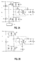
- FIGs 1a and 1b are circuits illustrating prior art type clamp mode flyback DC/DC converters, where Llk and Lm are leakage inductance and magnetizing inductance, respectively, of the transformer T as seen from the primary side of the transformer.
- Capacitors Cs1 and Cs2 are the junction capacitances of the MOSFET switches Q1 and Q2, respectively.
- the clamping capacitor C2 is connected to the positive terminal of the DC input voltage.
- Inductors Llk, Lm, MOSFET switches Q1, Q2 and capacitor C2 form an auxiliary buck-boost converter.
- the clamping capacitor C2 is connected to the negative terminal (c) of the DC input voltage.
- Inductors Llk, Lm, MOSFET switches Q1 and Q2 and capacitor C2 form an auxiliary boost converter.
- the ON duty ratio of a switch is designed to be approximately 0.5. In that case the voltage stress of the semiconductor switch from equation (4) will be twice that of the input voltage, Vi. In high line voltage applications, high voltage MOSFET switches are then required, resulting in high cost for the MOSFET switches and a limited selection thereof.
- a known converter similar to that shown in Fig. 1a herein is the clamp mode flyback DC/DC converter described in U.S. Patent 5,066,900.
- the circuit in Fig. 5 of this patent is similar to the prior art circuit in Fig. 1a herein except that the secondary side of the transformer is a forward output instead of a flyback output, and the position of the high-side circuit is exchanged with the position of the low-side circuit.
- This DC/DC converter employs one or more semiconductor switches.
- a problem that occurs with such circuits is that the voltage that the semiconductor switch has to withstand is approximately twice that of the DC input voltage. This is termed herein the "voltage stress" of the switch.
- a converter is shown in Fig. 1 of U.S. Patent 5,126,931 which is almost identical to the prior art circuit in Fig. 1b herein, except that the secondary side of the transformer is a forward output instead of a flyback output.
- This converter includes a boost clamp but suffers from the same drawbacks as the circuit of U.S. Patent 5,066,900.
- U.S. Patent 4,959,764 and EP 0 508 664 A1 describe other examples of the same types of converters, which can be characterized as belonging to one of the following types: forward or flyback converter with a boost clamp or a buck-boost clamp. None of them is suitable for high voltage off-line power supplies because of the high voltage stress in the power switches.
- the circuit shown in Fig. 3 of U.S. Patent 5,057,986 is a converter circuit which subjects its power switches to a lower voltage stress compared with the circuits of the above-identified patents.
- the leakage inductance is made as small as possible so that energy can be transferred effectively to the secondary side of the transformer, which produces a step change in the primary winding current of the voltage transformer.
- This step change usually results in excessive electromagnetic interference (EMI) noise emission, making it difficult to use such a converter as a power supply in, for example, a television receiver or a VCR.
- EMI electromagnetic interference
- the converter of this patent has only two operation stages (see Figs. 5 and 6 of the patent) and a voltage conversion ratio Vout/Vin which is linear function of the duty ratio D (see equation (3) of the patent).
- Another object of the invention is to provide a DC/DC converter circuit exhibiting reduced radiated and conducted EMI noise emission.
- Still another object of the invention is to provide a DC/DC converter circuit of the pulse width modulator (PWM) type exhibiting zero-voltage-switching (ZVS) to reduce switching losses, especially at high operating frequencies, and thus improve the circuit efficiency, and in which the incorporated semiconductor switches undergo voltage stresses that do not exceed the line voltage and which is suitable for high voltage off-line low noise power supply applications.
- PWM pulse width modulator
- ZVS zero-voltage-switching
- a further object of the invention is to provide a DC/DC converter circuit having a predetermined linkage inductance for the output transformer which is chosen so as to smooth the primary side current and thereby achieve low EMI noise emission.
- a still further object of the invention is to provide a DC/DC converter circuit having a novel mode of operation including three distinct operation modes for each operating cycle.
- Another object of the invention is to provide a converter having a voltage conversion ratio (Vout/Vin) which is a non-linear function of the duty ratio (D) and which depends upon circuit parameters such as operating frequency, leakage inductance and magnetizing inductance.
- Vout/Vin voltage conversion ratio
- D duty ratio
- a first aspect of the invention provides a DC-DC converter circuit as defined in Claim 1.
- a second aspect of the invention provides a method of operating a DC-DC converter circuit as defined in Claim 10.
- a third aspect of the invention provides a DC-DC converter circuit as defined in Claim 11.
- a fourth aspect of the invention provides a DC-DC converter circuit as defined in Claim 15.
- Advantageous embodiments of the invention are defined in the depedent Claims.
- One aspect of the invention is based on the recognition that, to avoid excessive radiated EMI emissions, the circuit is configured to provide smooth primary-side current in the converter transformer.
- Another aspect of the present invention is based on the recognition that smooth primary side current in the converter transformer can be achieved together with reduced voltage stress on the power semiconductor switches with a converter circuit providing three operation stages during each switching cycle.
- Still another aspect of the present invention is based on the recognition that, contrary to the previous understandings of the operation of such converter circuits, a certain amount of leakage inductance is desirable in order to smooth the primary-side transformer current and thereby lessen the EMI.
- both the first and second switches are open for a short time periode (dead-time).
- the operation of the converter circuits of the invention are somewhat similar to that of the known half-bridge, ZVS, PWM, clamp mode, flyback dc-dc converter in its basic operation.
- the major differences between converters of the invention and those of the prior art are that, in the converter of the invention, a smooth primary-side current is achieved instead of a current with a step change. Such a current can reduce both conducted and radiated EMI noise emission.
- the converter of the invention is characterized by three operation stages instead of two stages.
- the voltage conversion ratio Vout/Vin of the converter of the invention is a non-linear function of ON duty ratio D of the first switch.
- the converter of the invention is suitable for high-voltage, off-line (such as Europe line), low noise power supply applications.
- the invention also includes the method of operating the various embodiments of the circuits as described below.
- the leakage inductance if intrinsic, can be adjusted, for example, increased, by winding the primary winding and the secondary winding side by side. If additional inductance is desired, an extrinsic inductor can be added in series. Similarly, the magnetizing inductance can be controlled by the transformer geometry and reduced, if desired, by adding an inductor in parallel.
- Fig. 2(a) shows a first embodiment of the invention having first and second input terminals (b) and (c), respectively, for connection to a source of DC supply voltage, such as the output of a rectifier circuit (not shown) having its input connected to the conventional 50 Hz or 60 Hz AC supply voltage generally available in Europe and the U.S.A., respectively.
- Input terminal (b) is positive (+) with respect to input terminal (c) (-).
- First and second capacitors C1 and C2 are connected in series circuit across the DC input voltage terminals (b) and (c).
- First and second semiconductor switches Q1 and Q2, for example, MOSFET devices, are connected in a second series circuit across the DC input terminals.
- a junction point (a) between capacitors C1 and C2 is connected to one end of the primary winding Np of an output transformer (T) and the junction point (d) between the MOSFET switches Q1 and Q2 is connected to the other end of the transformer primary winding.
- the transformer leakage inductance Llk is represented by an inductor in the connection between junction point (a) and the one end of the transformer primary winding and the transformer magnetizing inductance Lm is represented by an inductor in parallel with the primary winding.
- the transformer secondary winding Ns is connected via a rectifier diode D to one end of a smoothing capacitor Co, and to one end of a load represented by a resistor R.
- a control circuit 10 has output terminals connected to respective control electrodes of the semiconductor switches Q1 and Q2 in order to alternately operate same in the manner to be disclosed below with reference to the waveforms shown in Fig. 5.
- Fig. 2(b) shows a modified form of the embodiment of the invention shown in Fig. 2(a).
- the main differences are that the capacitor C2 is connected directly across the DC supply voltage input terminals (b) and (c), and a blocking capacitor C1 is now connected between the second input terminal (c) and the terminal (a) connected to the bottom end of the output transformer primary winding Np.
- the junction (d) between semiconductor switches Q1 and Q2 is now connected to the top end of the transformer primary winding.
- the dot symbols on the transformer windings are aligned and again show the polarity of the transformer windings, which is opposite to that shown in Fig. 2(a). It is also possible to reverse the winding polarity in Fig. 2(b) to that of Fig. 2(a) where the dotted secondary is opposed to the dotted primary.
- the control electrodes of transistors Q1 and Q2 will be connected to the output of a control circuit (not shown) in the manner of Fig. 2(a).
- FIGs. 2(a) and 2(b) the input voltage is applied across terminals (b) and (c) instead of terminals (a) and (c) as in Figs. 1(a) and 1(b).
- Figure 2(a) is the circuit of a half-bridge zero voltage switched pulse width modulated (ZVS-PWM) flyback converter and
- Fig. 2(b) is the half-bridge converter version with a blocking capacitor.
- the voltage stress on the MOSFET switches is reduced to the value of the input voltage, which makes the selection of the MOSFET switches cheaper and more flexible.
- These circuits are particularly suitable for 220V AC applications.
- MOSFET switches are represented for the sake of simplicity as mechanical on-off switches Q1 and Q2.
- the first (top) waveform shows the control voltage which the control circuit 10 (Fig. 2(a)) applies to the control electrode of MOSFET switch Q1, i.e., V gs1 for transistor Q1.
- the second waveform in Fig. 5 is the control voltage applied to the control electrode of MOSFET switch Q2, i.e., V gs2 for transistor Q2.
- the waveform is high, the corresponding switch Q1 or Q2 is on, i.e., closed in Fig. 3, and when the waveform is low the switches Q1 and Q2 are off, i.e., open in Fig. 3.
- the third waveform of Fig. 5 shows, as a function of time, the transformer magnetizing current im and the leakage inductance current ilk, where Ip is a peak current value.
- the fourth (bottom) line of Fig. 5 shows the diode current waveform id, also as a function of time.
- the magnetizing current im keeps on decreasing as before, while the leakage current ilk now is increasing.
- the diode current id now linearly decreases, as shown in the bottom waveform of Fig. 5.
- the diode current is a triangular waveform with a linear rise and a linear fall, leading to reduced EMI noise generation.
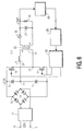
- Fig. 6 shows an embodiment of the invention which has special utility in a European TV receiver.
- This converter circuit is a 100W, 130V power supply operable at 100KHz.
- Input terminals 11, 12 will be connected to the 220V AC supply lines.
- An EMI filter 13 is connected between the input terminals and a bridge rectifier 14.
- the output terminals of the bridge rectifier supply a DC voltage of 310V with terminal 15 supplying the positive voltage.
- First and second capacitors 16 and 17 are connected in a first series circuit across the DC output terminals of bridge rectifier 14. For example, these capacitors may be 100 ⁇ F each.
- a second series circuit of MOSFET switching devices 18 and 19 is connected in parallel with the first circuit 16, 17.
- the switching transistors 18 and 19 may, for example, each be an IRF 720 device.
- a junction point 20 between capacitors 16 and 17 is connected to the top end of primary winding 21 of a transformer 22 and a junction point 23 between transistors 18 and 19 is connected to the bottom end of the transformer.
- the transformer leakage inductance 24 is connected between junction point 20 and the top end of primary winding 21.
- the leakage inductance can be a separate external inductor or a combination of the transformer leakage inductance plus a series connected external inductor. In one example, the leakage inductance was 42 ⁇ H.
- the magnetizing inductance Lm of the transformer (not shown) is, in the given example, 0.42mH. It has been found that best results are obtained when the leakage inductance is 10% or more of the magnetizing inductance (Lm). This then provides for zero voltage switching and for a smooth rectifier current.
- the transformer secondary winding is coupled at one end via a diode 25 to one end of a capacitor 27 and a load 26.
- the other end of the secondary winding is coupled to the other ends of capacitor 27 and load 26.
- the transformer turns ratio is 1:1
- the diode 25 is a BYM 26C device
- capacitor 27 is 10 ⁇ F
- the load 26 can be represented by a resistor of 168-1680 ohms.
- a DC voltage of +130V is obtained at the load.
- the +130V terminal of the load is connected to an input of an isolated voltage sensor 28.
- the output of the voltage sensor is coupled to an input of a PWM controller 29, for example, of the type UC3823.
- the output of the PWM controller is in turn coupled to an input of a half-bridge MOSFET driver 30, for example, of the type IR2111.
- the driver 30 in turn has first and second outputs connected to the control electrodes of semiconductor switches 18 and 19, respectively.
- the controller and driver supply the drive waveforms that produce the novel three stage operation modes described above.
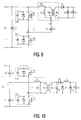
- Fig. 8(a) shows an equivalent circuit of the invention while Fig. 8(b) shows waveforms similar to Fig. 5 describing the operation sequence of zero voltage switching, where in Fig. 8(a) a current source 31 is used to represent the current flowing through the leakage inductor.
- Fig. 8(b) the third waveform represents the leakage inductor current Ilk versus time and the fourth waveform represents the voltage vd at the junction point (d) of the converter.
- Fig. 9 shows another embodiment of the invention in which the blocking capacitor C1 is now connected between the bottom terminal (a) of the transformer primary winding and the junction point (d) between the MOSFET switches Q1 and Q2.
- D represents the on duty ratio of MOSFET switch Q2. If the transformer winding polarity is reversed to that of Fig. 2(a), i.e., the dot for primary winding Np is now at the top end of the primary winding, then equation (10) holds true for the circuit of Fig. 9.
- Fig. 10 shows a half-bridge forward converter in accordance with the invention.
- This circuit is similar to that in Fig. 2(a) except that the transformer winding polarity is reversed, an inductor Lo is connected in series with the diode, now labelled D1, a capacitor Cd is connected across the transformer secondary winding Ns and a diode D2 is connected with opposite polarity between the cathode of diode D1 and the bottom end of the secondary winding Ns.
- the half-bridge ZVS PWM forward DC/DC converter of Fig. 10 operates on the same concepts as those described above for Figs. 2(a) and 2(b).
- Another possible variation of the invention is to provide a multi-output converter which employs plural secondary windings magnetically coupled to the primary winding and each secondary winding having a separate output circuit similar to the output circuit of Fig. 2(a), including a diode D and a capacitor Co, and with each output circuit connected to a separate load resistance.
- the invention provides significant advantages over prior art converters.
- the invention provides reduced voltage stress on the semiconductor switches Q1, Q2, reduced EMI noise and switching losses, a low di/dt is obtained for the rectifying diode D, and zero-voltage-switching can be provided.
- Advantages over the resonant flyback type of converter includes reduced voltage and current stress on the semiconductor switch, a low value of di/dt for the rectifying diode D, and constant frequency pulse width modulation is possible in order to provide output regulation.
- Advantages over the clamp mode flyback converter include reduced voltage stress on the semiconductor switches Q1, Q2 and reduced voltage stress on the clamp capacitor.
- the leakage inductance and/or the magnetizing inductance can be external inductors.
- the inherent semiconductor switch capacitances Cs1 and Cs2 can be external capacitors.
- Other types of semiconductor switching types can be used instead of the disclosed MOSFET switches Q1 and Q2, such as bipolar junction transistors, isolated-gate bipolar junction transistors and so on.
- the transformer polarity can be reversed.
- the blocking capacitor C1 in Fig. 2(b) can be connected differently.
- the inventive concept is also applicable to a forward converter.
Abstract
Description


Claims (15)
- A DC-DC converter circuit comprising:a) a transformer having a primary, a secondary, and a magnetizing inductance connected in parallel with the primary,b) an auxiliary inductance connected in series with the transformer primary,c) an input having first and second terminals for connection to a dc input voltage source,d) a first switch connecting the input second terminal to the transformer primary,e) a second switch connecting the input first terminal to the transformer primary,f) a first capacitor connected in series with the first switch and the transformer primary,g) a second capacitor connected in series with the second switch and the transformer primary,h) a rectifier connected to the transformer secondary,i) an output connected to the rectifier and the transformer secondary, andj) a controller for controlling operation of the switches such that:i) during a first operation period, the first switch is open and the second switch is closed causing currents through both the magnetizing inductance and auxiliary inductance to decrease, turning on the rectifier,ii) during a second operation period, the first switch is closed and the second switch is open causing the current through the magnetizing inductance to continue to decrease while causing the current through the auxiliary inductance to increase, maintaining the rectifier on, andiii) during a third operation period, while the first switch is closed and the second switch is open, when the current through the auxiliary inductance reaches the current through the magnetizing inductance, the current through both the auxiliary inductance and magnetizing inductance increase, turning off the rectifier.
- A DC-DC converter circuit as claimed in Claim 1, wherein each of the switches comprises is a MOSFET having a body diode and an intrinsic junction capacitance in parallel with each of the MOSFETs.
- A DC-DC converter circuit as claimed in Claim 1, wherein the transformer has a dotted and an undotted side of the primary and a dotted secondary opposed to the dotted primary, the second capacitor and the second switch are connected to the positive terminal of the input, the first capacitor and the first switch are connected to the negative terminal of the input, both the first and second switches are connected via a common node to the undotted side of the primary, and the first and second capacitors are connected via a common node to the dotted side of the primary.
- A DC-DC converter circuit as claimed in Claim 1, wherein the transformer has a dotted and an undotted side of the primary and a dotted secondary aligned with the dotted primary, the second capacitor and the second switch are connected to the positive terminal of the input, the first capacitor and the first switch are connected to the negative terminal of the input, both the first and second switches are connected via a common node to the undotted side of the primary, the first capacitor is connected to the dotted side of the primary, and the second capacitor is connected across the input.
- A DC-DC converter circuit as claimed in Claim 1, wherein the transformer has a dotted and an undotted side of the primary and a dotted secondary aligned with the dotted primary, the second capacitor and the second switch are connected to the positive terminal of the input, the first capacitor and the first switch are connected to the negative terminal of the input, both the first and second switches are connected via a common node to the dotted side of the primary, and the first and second capacitors are connected via a common node to the undotted side of the primary.
- A DC-DC converter circuit as claimed in Claim 1, wherein the transformer has a dotted and an undotted side of the primary and a dotted secondary opposed to the dotted primary, the second capacitor and the second switch are connected to the positive terminal of the input, the first capacitor and the first switch are connected to the negative terminal of the input, both the first and second switches are connected via a common node to the dotted side of the primary, the first capacitor is connected to the undotted side of the primary, and the second capacitor is connected across the input.
- A DC-DC converter circuit as claimed in Claim 1, wherein the transformer has a dotted and an undotted side of the primary and a dotted secondary aligned with the dotted primary, the second switch is connected to the positive terminal of the input, the second capacitor is connected between the dotted side of the primary and a common node of both switches, the first capacitor and the first switch are connected to the negative terminal of the input, and the first capacitor is connected across the input.
- A DC-DC converter circuit as claimed in Claim 1, wherein the transformer has a dotted and an undotted side of the primary and a dotted secondary opposed to the dotted primary, the second switch is connected to the positive terminal of the input, the first capacitor and the first switch are connected to the negative terminal of the input, the second capacitor is connected via a common node of both switches to the undotted side of the primary, and the first capacitor is connected across the input.
- A DC-DC converter circuit as claimed in Claim 1, wherein the controller further controls the operation of the switches such that at the initial part of the first operation period, both the first and second switches are open for a short dead-time to achieve zero-voltage switching, and at the initial part of the second operation period, both the first and second switches are open for a short dead-time to achieve zero-voltage switching.
- A method of operating a DC-DC converter circuit comprising:a) a transformer having a primary, a secondary, and a magnetizing inductance connected in parallel with the primary,b) an auxiliary inductance connected in series with the transformer primary,c) an input having first and second terminals for connection to a dc input voltage source,d) a first switch connecting the input second terminal to the transformer primary,e) a second switch connecting the input first terminal to the transformer primary,f) a first capacitor connected in series with the first switch and the transformer primary,g) a second capacitor connected in series with the second switch and the transformer primary,h) a rectifier connected to the transformer secondary,i) an output connected to the rectifier and the transformer secondary,j) a controller for controlling operation of the switches, said method comprising the steps:i) during a first operation period, opening the first switch and closing the second switch causing currents through both the magnetizing inductance and auxiliary inductance to decrease, turning on the rectifier,ii) during a second operation period, closing the first switch and opening the second switch causing the currents through the magnetizing inductance to continue to decrease while causing the current through the auxiliary inductance to increase, maintaining the rectifier on,iii) during a third operation period, maintaining the first switch closed and the second switch open, when the current through the auxiliary inductance reaches the current through the magnetizing inductance, the current through both the auxiliary inductance and magnetizing inductance increase, turning off the rectifier,iv) at the initial part of the first and second operation periods, opening both the first and second switches for a short dead-time to achieve zero-voltage switching.
- A DC-DC converter circuit comprising:a) a transformer having a primary, a secondary, and a magnetizing inductance connected in parallel with the primary,b) an auxiliary inductance connected in series with the transformer primary,c) an input having first and second terminals for connection to a dc input voltage source,d) a first switch connecting the input second terminal to the transformer primary,e) a second switch connecting the input first terminal to the transformer primary,f) a first capacitor connected in series with the first switch and the transformer primary,g) a second capacitor connected in series with the second switch and the transformer primary,h) a rectifier connected to the transformer secondary,i) an output connected to the rectifier and the transformer secondary,j) a controller for controlling operation of the switches such that:whereby the linear rise and fall of rectifier current reduces EMI noise generation and any voltage stress of the switches is reduced.i) during an initial part of a first operation period, both the first and second switches are open for a short dead-time to achieve zero-voltage switching,ii) during the remainder of the first operation period, the first switch is open and the second switch is closed turning on the rectifier and causing a current through the rectifier to rise linearly,iii) during an initial part of the second operation period, both the first and second switches are open for a short dead-time to achieve zero-voltage switching,iv) during the remainder of the second operation period, the first switch is closed and the second switch is open causing the current through the rectifier to fall linearly,v) during a third operation period, while the first switch is closed and the second switch is open, the rectifier is turned off,
- A DC-DC converter circuit as claimed in Claim 11, wherein the inductance of the auxiliary inductance is at least 10% that of the magnetizing inductance.
- A DC-DC converter circuit claimed in Claim 11, wherein;the first and second capacitors are connected in a first series circuit across the first and second input terminals,the first and second switches are connected in a second series circuit across the first and second input terminals,a junction point between the first and second capacitors is connected via the auxiliary inductance to one end of the transformer primary, anda junction between the first and second switches is connected to a second end of the transformer primary.
- A DC-DC converter circuit as claimed in Claim 11, wherein;the second capacitor is connected across the first and second input terminals,a junction point between the first and second switches is connected via the auxiliary inductance to a first end of the transformer primary, andthe first capacitor is connected between the second input terminal and a second end of the transformer primary.
- A DC-DC converter circuit comprising:a transformer having a primary, a secondary, and a magnetizing inductance connected in parallel with the primary,an auxiliary inductance connected in series with the transformer primary,first and second input terminals for connection to a DC source of supply voltage,first and second switches connected in series circuit across the input terminals,means connecting the auxiliary inductance between the first input terminal and a first end of the transformer primary winding,means connecting the first switch to the second input terminal,means connecting a first capacitor between a junction point between the first and second switches and a second end of the transformer primary winding,means connecting a second capacitor across the input terminals, anda diode-capacitor output circuit coupling the transformer secondary winding to output terminals of the converter circuit.
Applications Claiming Priority (2)
| Application Number | Priority Date | Filing Date | Title |
|---|---|---|---|
| US08/773,117 US5808879A (en) | 1996-12-26 | 1996-12-26 | Half-bridge zero-voltage-switched PWM flyback DC/DC converter |
| US773117 | 1996-12-26 |
Publications (3)
| Publication Number | Publication Date |
|---|---|
| EP0851566A2 true EP0851566A2 (en) | 1998-07-01 |
| EP0851566A3 EP0851566A3 (en) | 1999-01-07 |
| EP0851566B1 EP0851566B1 (en) | 2003-03-19 |
Family
ID=25097256
Family Applications (1)
| Application Number | Title | Priority Date | Filing Date |
|---|---|---|---|
| EP97204010A Expired - Lifetime EP0851566B1 (en) | 1996-12-26 | 1997-12-18 | Half-bridge zero-voltage-switched PWM flyback DC/DC converter |
Country Status (3)
| Country | Link |
|---|---|
| US (1) | US5808879A (en) |
| EP (1) | EP0851566B1 (en) |
| DE (1) | DE69719945T2 (en) |
Cited By (10)
| Publication number | Priority date | Publication date | Assignee | Title |
|---|---|---|---|---|
| EP1128537A2 (en) * | 2000-02-25 | 2001-08-29 | Murata Manufacturing Co., Ltd. | Switching power supply apparatus |
| EP1248356A2 (en) * | 2001-04-06 | 2002-10-09 | Philips Corporate Intellectual Property GmbH | Power supply circuit with a DC/DC-converter |
| WO2003043165A2 (en) * | 2001-11-13 | 2003-05-22 | Synqor, Inc. | Half-bridge isolation stage topologies |
| EP1737278A2 (en) * | 2005-06-21 | 2006-12-27 | Patent-Treuhand-Gesellschaft für elektrische Glühlampen mbH | Filtering circuit for improving emi shielding |
| EP1521366A3 (en) * | 2003-09-30 | 2008-08-06 | Power Integrations, Inc. | Method and apparatus for simplifying the control of a switch |
| CN100421344C (en) * | 2004-01-30 | 2008-09-24 | 雅达电子国际有限公司 | Zero-voltage switching half-bridge DC-DC converter topology by utilizing the transformer leakage inductance trapped energy |
| EP1971192A3 (en) * | 2007-03-15 | 2012-06-27 | Vossloh-Schwabe Deutschland GmbH | Control gear with improved EMC compliance |
| WO2019075379A1 (en) * | 2017-10-12 | 2019-04-18 | Ionel Jitaru | Energy recovery from the leakage inductance of the transformer in a flyback converter |
| WO2020021020A1 (en) * | 2018-07-26 | 2020-01-30 | Infineon Technologies Austria Ag | Active clamp flyback converter with variable resonance frequency |
| CN111786559A (en) * | 2019-04-03 | 2020-10-16 | 深圳市正弦电气股份有限公司 | Double-tube flyback power circuit |
Families Citing this family (55)
| Publication number | Priority date | Publication date | Assignee | Title |
|---|---|---|---|---|
| US7269034B2 (en) | 1997-01-24 | 2007-09-11 | Synqor, Inc. | High efficiency power converter |
| KR100455651B1 (en) * | 1997-08-08 | 2005-01-17 | 삼성전자주식회사 | Multi-output dc/dc voltage converting apparatus and liquid crystal display, including multi-output dc/dc voltage converter for generating main power through choke system and auxiliary power through flyback system |
| KR100297340B1 (en) * | 1997-11-18 | 2001-10-26 | 이형도 | Asymmetry flyback converter |
| US5991170A (en) * | 1998-02-03 | 1999-11-23 | Sony Corporation | Equipment and method for transmitting electric power |
| CA2249755C (en) * | 1998-10-02 | 2006-12-12 | Praveen K. Jain | Full bridge dc-dc converters |
| US6862437B1 (en) * | 1999-06-03 | 2005-03-01 | Tyco Electronics Corporation | Dual band tuning |
| US6246592B1 (en) | 1999-08-10 | 2001-06-12 | Texas Instruments Incorporated | Unique power supply architecture with cascaded converters for large input-to-output step-down ratio |
| US6349044B1 (en) * | 1999-09-09 | 2002-02-19 | Virginia Tech Intellectual Properties, Inc. | Zero voltage zero current three level dc-dc converter |
| US6147881A (en) * | 1999-09-29 | 2000-11-14 | Hua-In Co., Ltd. | Resonant switching power supply |
| JP3430107B2 (en) * | 2000-02-23 | 2003-07-28 | エヌイーシ−カスタムテクニカ株式会社 | Leakage current suppression circuit and power supply device using the same |
| US6407935B1 (en) * | 2000-05-30 | 2002-06-18 | Koninklijke Philips Electronics N.V. | High frequency electronic ballast with reactive power compensation |
| SE0101125L (en) * | 2001-03-30 | 2002-10-01 | Ragnar Joensson | Control device and method for a transistor switching circuit |
| DE10128687A1 (en) * | 2001-06-13 | 2002-12-19 | Philips Corp Intellectual Pty | DC converter |
| JP2003133095A (en) * | 2001-10-30 | 2003-05-09 | Mitsubishi Electric Corp | Discharge lamp lighting device |
| US6836414B1 (en) | 2002-10-17 | 2004-12-28 | University Of Central Florida | PWM half-bridge converter with dual-equally adjustable control signal dead-time |
| US7209370B2 (en) * | 2003-08-09 | 2007-04-24 | Astec International Limited | Circuit for reducing losses at light load in a soft switching full bridge converter |
| US7149096B2 (en) * | 2004-02-18 | 2006-12-12 | Astec International Limited | Power converter with interleaved topology |
| US7030587B2 (en) * | 2004-04-09 | 2006-04-18 | Visteon Global Technologies, Inc. | Configuration of converter switches and machine coils of a switched reluctance machine |
| US6982887B2 (en) * | 2004-04-26 | 2006-01-03 | Astec International Limited | DC-DC converter with coupled-inductors current-doubler |
| TWI268041B (en) * | 2004-09-09 | 2006-12-01 | Delta Electronics Inc | Input stage circuit of a three-level DC/DC converter |
| JP4371042B2 (en) * | 2004-11-11 | 2009-11-25 | サンケン電気株式会社 | Switching power supply |
| US7345378B2 (en) * | 2004-12-07 | 2008-03-18 | Intersil Americas Inc. | Power supply circuit containing multiple DC—DC converters having programmable output current capabilities |
| US7196916B2 (en) * | 2005-02-14 | 2007-03-27 | University Of Central Florida Research Foundation | Alternated duty cycle control method for half-bridge DC-DC converter |
| US7375994B2 (en) * | 2005-10-11 | 2008-05-20 | Texas Instruments Incorporated | Highly efficient isolated AC/DC power conversion technique |
| KR101374033B1 (en) * | 2005-11-11 | 2014-03-12 | 엘앤드엘 엔지니어링 엘엘씨 | Non-linear pwm controller for dc-to-dc converters |
| US8395365B2 (en) | 2005-11-11 | 2013-03-12 | Maxim Integrated Products, Inc. | Non-linear PWM controller |
| JP4876624B2 (en) * | 2006-02-22 | 2012-02-15 | 富士通セミコンダクター株式会社 | Power supply device control circuit, power supply device and control method therefor |
| US7471524B1 (en) | 2006-05-26 | 2008-12-30 | University Of Central Florida Research Foundation, Inc. | Isolated DC-DC converters with high current capability |
| CA2655013A1 (en) * | 2008-02-22 | 2009-08-22 | Queen's University At Kingston | Current-source gate driver |
| KR100966972B1 (en) * | 2008-07-17 | 2010-06-30 | 삼성전기주식회사 | Variable switching frequency type power supply |
| ATE529939T1 (en) * | 2008-10-27 | 2011-11-15 | Abb Research Ltd | CONVERTER CIRCUIT AND UNIT AND SYSTEM HAVING SUCH A CONVERTER CIRCUIT |
| EP2421136B1 (en) * | 2009-04-14 | 2019-05-08 | Murata Manufacturing Co., Ltd. | Switching power supply unit |
| EP2421137B1 (en) * | 2009-04-14 | 2019-05-08 | Murata Manufacturing Co., Ltd. | Switching power supply unit |
| EP2449859A1 (en) * | 2009-06-30 | 2012-05-09 | Koninklijke Philips Electronics N.V. | Circuit for converting dc into ac pulsed voltage |
| EP2476191A1 (en) * | 2009-09-08 | 2012-07-18 | Koninklijke Philips Electronics N.V. | Switching device for an x-ray generator |
| SE534975C2 (en) * | 2009-10-16 | 2012-03-06 | Tsc Innovation Ab | Method and apparatus for installing and repairing insulated pipe lines |
| KR20110138068A (en) * | 2010-06-18 | 2011-12-26 | 페어차일드코리아반도체 주식회사 | Powerfactor compensation converter and driving method thereof |
| IT1403601B1 (en) | 2010-12-22 | 2013-10-31 | St Microelectronics Srl | CONTROL DEVICE FOR A DC-DC CONVERTER. |
| KR101310551B1 (en) * | 2011-11-11 | 2013-09-23 | 성균관대학교산학협력단 | Converter, inverter and controlling method for converter |
| CN103840657B (en) * | 2012-11-23 | 2016-08-31 | 台达电子工业股份有限公司 | The balance of voltage method of power supply changeover device and input capacitance |
| US10199950B1 (en) | 2013-07-02 | 2019-02-05 | Vlt, Inc. | Power distribution architecture with series-connected bus converter |
| US9537338B2 (en) | 2014-09-16 | 2017-01-03 | Navitas Semiconductor Inc. | Level shift and inverter circuits for GaN devices |
| US9571093B2 (en) | 2014-09-16 | 2017-02-14 | Navitas Semiconductor, Inc. | Half bridge driver circuits |
| US9276413B1 (en) * | 2014-09-25 | 2016-03-01 | Navitas Semiconductor, Inc. | Soft switched single stage wireless power transfer |
| US9379620B2 (en) * | 2014-10-02 | 2016-06-28 | Navitas Semiconductor Inc. | Zero voltage soft switching scheme for power converters |
| JP6372607B2 (en) * | 2015-02-17 | 2018-08-15 | 株式会社村田製作所 | DC-DC converter |
| US9831867B1 (en) | 2016-02-22 | 2017-11-28 | Navitas Semiconductor, Inc. | Half bridge driver circuits |
| US10401885B2 (en) * | 2017-08-18 | 2019-09-03 | Rolls-Royce North American Technologies Inc. | DC to DC converter output bus voltage control system |
| IL255948A (en) | 2017-11-27 | 2018-01-31 | Abramovici Tal | Constant frequency dc/dc power converter |
| TWI742358B (en) * | 2018-05-04 | 2021-10-11 | 德商伍爾特電子eiSos有限公司 | A power converter and a circuit forming a portion thereof |
| WO2020104597A1 (en) * | 2018-11-22 | 2020-05-28 | Danmarks Tekniske Universitet | Isolated dc-dc power converter with adjustable turns ratio |
| US10833616B1 (en) * | 2019-11-22 | 2020-11-10 | Rolls-Royce Marine North America Inc. | Gas turbine engine generator power management control system |
| CN111600477B (en) * | 2020-06-30 | 2023-04-25 | 敏业信息科技(上海)有限公司 | Noise suppression circuit for reinjection cancellation |
| CN113330672B (en) * | 2020-12-23 | 2022-09-09 | 深圳欣锐科技股份有限公司 | Charging system and car |
| KR20220151671A (en) * | 2021-02-10 | 2022-11-15 | 후아웨이 디지털 파워 테크놀러지스 컴퍼니 리미티드 | DC-to-DC converters, electronics and chargers |
Citations (5)
| Publication number | Priority date | Publication date | Assignee | Title |
|---|---|---|---|---|
| JPS63186561A (en) * | 1987-01-28 | 1988-08-02 | Densetsu:Kk | Full-wave converter |
| US5245520A (en) * | 1991-10-10 | 1993-09-14 | Paul Imbertson | Asymmetrical duty cycle power converter |
| US5490052A (en) * | 1992-04-24 | 1996-02-06 | Matsushita Electric Industrial Co., Ltd. | Switching power supply |
| WO1996015579A1 (en) * | 1994-11-16 | 1996-05-23 | SIEMENS AKTIENGESELLSCHAFT öSTERREICH | Switching power converter |
| JPH08289540A (en) * | 1995-04-17 | 1996-11-01 | Sanken Electric Co Ltd | Switching power supply system |
Family Cites Families (4)
| Publication number | Priority date | Publication date | Assignee | Title |
|---|---|---|---|---|
| US4533986A (en) * | 1983-10-31 | 1985-08-06 | General Electric Company | Compact electrical power supply for signal processing applications |
| US5066900A (en) * | 1989-11-14 | 1991-11-19 | Computer Products, Inc. | Dc/dc converter switching at zero voltage |
| US5126931A (en) * | 1990-09-07 | 1992-06-30 | Itt Corporation | Fixed frequency single ended forward converter switching at zero voltage |
| US5471376A (en) * | 1993-03-05 | 1995-11-28 | Digital Equipment Corporation | Low-loss active voltage-clamp circuit for single-ended forward PWM converter |
-
1996
- 1996-12-26 US US08/773,117 patent/US5808879A/en not_active Expired - Fee Related
-
1997
- 1997-12-18 EP EP97204010A patent/EP0851566B1/en not_active Expired - Lifetime
- 1997-12-18 DE DE69719945T patent/DE69719945T2/en not_active Expired - Fee Related
Patent Citations (5)
| Publication number | Priority date | Publication date | Assignee | Title |
|---|---|---|---|---|
| JPS63186561A (en) * | 1987-01-28 | 1988-08-02 | Densetsu:Kk | Full-wave converter |
| US5245520A (en) * | 1991-10-10 | 1993-09-14 | Paul Imbertson | Asymmetrical duty cycle power converter |
| US5490052A (en) * | 1992-04-24 | 1996-02-06 | Matsushita Electric Industrial Co., Ltd. | Switching power supply |
| WO1996015579A1 (en) * | 1994-11-16 | 1996-05-23 | SIEMENS AKTIENGESELLSCHAFT öSTERREICH | Switching power converter |
| JPH08289540A (en) * | 1995-04-17 | 1996-11-01 | Sanken Electric Co Ltd | Switching power supply system |
Non-Patent Citations (4)
| Title |
|---|
| FURUKAWA ET AL: "a high efficiency 150w DC/DC converter" PROCEEDINGS OF THE INTERNATIONAL TELECOMMUNICATIONS CONFERENCE(INTELEC), 30 October 1994 - 3 November 1994, pages 148-154, XP000623322 vancouver * |
| JOVANOVIC ET AL: "COMPARISON OF HALF-BRIDGE OFF-LINE, ZCS-QRC AND ZVS-MRC" IEEE-TRANSACTIONS ON AEROSPACE AND ELECTRONIC SYSTEMS, vol. 26, no. 2, March 1990, pages 326-335, XP000127759 new york * |
| PATENT ABSTRACTS OF JAPAN vol. 012, no. 465 (E-690) 07 December 1988 & JP 63 186 561 A (DENSETSU KK) 02 August 1988 * |
| PATENT ABSTRACTS OF JAPAN vol. 97, no. 3, 31 March 1997 & JP 08 289540 A (SANKEN ELECTRIC), 1 November 1996 * |
Cited By (20)
| Publication number | Priority date | Publication date | Assignee | Title |
|---|---|---|---|---|
| EP1128537A2 (en) * | 2000-02-25 | 2001-08-29 | Murata Manufacturing Co., Ltd. | Switching power supply apparatus |
| EP1128537A3 (en) * | 2000-02-25 | 2002-04-10 | Murata Manufacturing Co., Ltd. | Switching power supply apparatus |
| US6631079B2 (en) | 2000-02-25 | 2003-10-07 | Murata Manufacturing Co., Ltd. | Switching power supply apparatus having plural outputs and plural output voltage detection |
| EP1248356A2 (en) * | 2001-04-06 | 2002-10-09 | Philips Corporate Intellectual Property GmbH | Power supply circuit with a DC/DC-converter |
| EP1248356A3 (en) * | 2001-04-06 | 2004-04-21 | Philips Intellectual Property & Standards GmbH | Power supply circuit with a DC/DC-converter |
| WO2003043165A2 (en) * | 2001-11-13 | 2003-05-22 | Synqor, Inc. | Half-bridge isolation stage topologies |
| WO2003043165A3 (en) * | 2001-11-13 | 2004-02-12 | Synqor Inc | Half-bridge isolation stage topologies |
| US6927987B2 (en) | 2001-11-13 | 2005-08-09 | Synqor, Inc. | Half-bridge isolation stage topologies |
| US8441290B2 (en) | 2003-09-30 | 2013-05-14 | Power Integrations, Inc. | Method and apparatus for simplifying the control of a switch |
| EP1521366A3 (en) * | 2003-09-30 | 2008-08-06 | Power Integrations, Inc. | Method and apparatus for simplifying the control of a switch |
| US7466170B2 (en) | 2003-09-30 | 2008-12-16 | Power Integrations, Inc. | Method and apparatus for simplifying the control of a switch |
| US8063672B2 (en) | 2003-09-30 | 2011-11-22 | Power Integrations, Inc. | Method and apparatus for simplifying the control of a switch |
| US8278972B2 (en) | 2003-09-30 | 2012-10-02 | Power Integrations, Inc. | Method and apparatus for simplifying the control of a switch |
| CN100421344C (en) * | 2004-01-30 | 2008-09-24 | 雅达电子国际有限公司 | Zero-voltage switching half-bridge DC-DC converter topology by utilizing the transformer leakage inductance trapped energy |
| EP1737278A2 (en) * | 2005-06-21 | 2006-12-27 | Patent-Treuhand-Gesellschaft für elektrische Glühlampen mbH | Filtering circuit for improving emi shielding |
| EP1737278A3 (en) * | 2005-06-21 | 2014-04-23 | Patent-Treuhand-Gesellschaft für elektrische Glühlampen mbH | Filtering circuit for improving emi shielding |
| EP1971192A3 (en) * | 2007-03-15 | 2012-06-27 | Vossloh-Schwabe Deutschland GmbH | Control gear with improved EMC compliance |
| WO2019075379A1 (en) * | 2017-10-12 | 2019-04-18 | Ionel Jitaru | Energy recovery from the leakage inductance of the transformer in a flyback converter |
| WO2020021020A1 (en) * | 2018-07-26 | 2020-01-30 | Infineon Technologies Austria Ag | Active clamp flyback converter with variable resonance frequency |
| CN111786559A (en) * | 2019-04-03 | 2020-10-16 | 深圳市正弦电气股份有限公司 | Double-tube flyback power circuit |
Also Published As
| Publication number | Publication date |
|---|---|
| EP0851566B1 (en) | 2003-03-19 |
| US5808879A (en) | 1998-09-15 |
| DE69719945D1 (en) | 2003-04-24 |
| EP0851566A3 (en) | 1999-01-07 |
| DE69719945T2 (en) | 2004-01-22 |
Similar Documents
| Publication | Publication Date | Title |
|---|---|---|
| US5808879A (en) | Half-bridge zero-voltage-switched PWM flyback DC/DC converter | |
| US7023186B2 (en) | Two stage boost converter topology | |
| CN107979288B (en) | Forced zero-voltage switch flyback converter | |
| CN107979287B (en) | Zero-voltage switching inverter for main switch switching | |
| US5510974A (en) | High frequency push-pull converter with input power factor correction | |
| US6452814B1 (en) | Zero voltage switching cells for power converters | |
| US4720668A (en) | Zero-voltage switching quasi-resonant converters | |
| US7596007B2 (en) | Multiphase DC to DC converter | |
| US6995987B2 (en) | DC—DC converters providing reduced deadtime | |
| US7385833B2 (en) | Snubber circuit for a power converter | |
| Oruganti et al. | Soft-switched DC/DC converter with PWM control | |
| CN203691238U (en) | Electronic converter and related illuminating system | |
| US6442047B1 (en) | Power conversion apparatus and methods with reduced current and voltage switching | |
| US7859870B1 (en) | Voltage clamps for energy snubbing | |
| US7324355B2 (en) | Dc-DC converter | |
| EP1193851A1 (en) | Switching power supply device having series capacitance | |
| US7019988B2 (en) | Switching-type power converter | |
| US20040264224A1 (en) | Structure and method for an isolated boost converter | |
| Song et al. | Current-fed dual-bridge DC–DC converter | |
| US6185111B1 (en) | Switching power supply apparatus | |
| US6097614A (en) | Asymmetrical pulse width modulated resonant DC-DC converter with compensating circuitry | |
| US7362598B2 (en) | Synchronous rectifier gate drive shutdown circuit | |
| EP3916979A1 (en) | Switching converter | |
| US7609532B1 (en) | Phase-shifted PWM bridge with switchable inductors to maintain zero-voltage switching at light load | |
| WO2000028648A1 (en) | A high input voltage, high efficiency, fast transient voltage regulator module (vrm) |
Legal Events
| Date | Code | Title | Description |
|---|---|---|---|
| PUAI | Public reference made under article 153(3) epc to a published international application that has entered the european phase |
Free format text: ORIGINAL CODE: 0009012 |
|
| AK | Designated contracting states |
Kind code of ref document: A2 Designated state(s): DE FR GB |
|
| AX | Request for extension of the european patent |
Free format text: AL;LT;LV;RO;SI |
|
| RAP3 | Party data changed (applicant data changed or rights of an application transferred) |
Owner name: KONINKLIJKE PHILIPS ELECTRONICS N.V. |
|
| PUAL | Search report despatched |
Free format text: ORIGINAL CODE: 0009013 |
|
| AK | Designated contracting states |
Kind code of ref document: A3 Designated state(s): AT BE CH DE DK ES FI FR GB GR IE IT LI LU MC NL PT SE |
|
| AX | Request for extension of the european patent |
Free format text: AL;LT;LV;RO;SI |
|
| 17P | Request for examination filed |
Effective date: 19990707 |
|
| AKX | Designation fees paid |
Free format text: DE FR GB |
|
| 17Q | First examination report despatched |
Effective date: 19991005 |
|
| GRAG | Despatch of communication of intention to grant |
Free format text: ORIGINAL CODE: EPIDOS AGRA |
|
| GRAG | Despatch of communication of intention to grant |
Free format text: ORIGINAL CODE: EPIDOS AGRA |
|
| GRAH | Despatch of communication of intention to grant a patent |
Free format text: ORIGINAL CODE: EPIDOS IGRA |
|
| GRAH | Despatch of communication of intention to grant a patent |
Free format text: ORIGINAL CODE: EPIDOS IGRA |
|
| GRAA | (expected) grant |
Free format text: ORIGINAL CODE: 0009210 |
|
| AK | Designated contracting states |
Designated state(s): DE FR GB |
|
| REG | Reference to a national code |
Ref country code: GB Ref legal event code: FG4D |
|
| REG | Reference to a national code |
Ref country code: GB Ref legal event code: 746 Effective date: 20030321 |
|
| REF | Corresponds to: |
Ref document number: 69719945 Country of ref document: DE Date of ref document: 20030424 Kind code of ref document: P |
|
| ET | Fr: translation filed | ||
| REG | Reference to a national code |
Ref country code: FR Ref legal event code: D6 |
|
| PLBE | No opposition filed within time limit |
Free format text: ORIGINAL CODE: 0009261 |
|
| STAA | Information on the status of an ep patent application or granted ep patent |
Free format text: STATUS: NO OPPOSITION FILED WITHIN TIME LIMIT |
|
| 26N | No opposition filed |
Effective date: 20031222 |
|
| PGFP | Annual fee paid to national office [announced via postgrant information from national office to epo] |
Ref country code: GB Payment date: 20041222 Year of fee payment: 8 |
|
| PGFP | Annual fee paid to national office [announced via postgrant information from national office to epo] |
Ref country code: FR Payment date: 20041228 Year of fee payment: 8 |
|
| PGFP | Annual fee paid to national office [announced via postgrant information from national office to epo] |
Ref country code: DE Payment date: 20050215 Year of fee payment: 8 |
|
| PG25 | Lapsed in a contracting state [announced via postgrant information from national office to epo] |
Ref country code: GB Free format text: LAPSE BECAUSE OF NON-PAYMENT OF DUE FEES Effective date: 20051218 |
|
| PG25 | Lapsed in a contracting state [announced via postgrant information from national office to epo] |
Ref country code: DE Free format text: LAPSE BECAUSE OF NON-PAYMENT OF DUE FEES Effective date: 20060701 |
|
| GBPC | Gb: european patent ceased through non-payment of renewal fee |
Effective date: 20051218 |
|
| PG25 | Lapsed in a contracting state [announced via postgrant information from national office to epo] |
Ref country code: FR Free format text: LAPSE BECAUSE OF NON-PAYMENT OF DUE FEES Effective date: 20060831 |
|
| REG | Reference to a national code |
Ref country code: FR Ref legal event code: ST Effective date: 20060831 |