EP0854516A2 - Partially pinned photodiode for solid state image sensors - Google Patents
Partially pinned photodiode for solid state image sensors Download PDFInfo
- Publication number
- EP0854516A2 EP0854516A2 EP98200030A EP98200030A EP0854516A2 EP 0854516 A2 EP0854516 A2 EP 0854516A2 EP 98200030 A EP98200030 A EP 98200030A EP 98200030 A EP98200030 A EP 98200030A EP 0854516 A2 EP0854516 A2 EP 0854516A2
- Authority
- EP
- European Patent Office
- Prior art keywords
- photodiode
- region
- pixel
- conductivity type
- pinned
- Prior art date
- Legal status (The legal status is an assumption and is not a legal conclusion. Google has not performed a legal analysis and makes no representation as to the accuracy of the status listed.)
- Granted
Links
- 239000007787 solid Substances 0.000 title description 3
- 239000004065 semiconductor Substances 0.000 claims abstract description 10
- 239000003990 capacitor Substances 0.000 claims abstract description 3
- 230000006835 compression Effects 0.000 claims description 4
- 238000007906 compression Methods 0.000 claims description 4
- 238000004519 manufacturing process Methods 0.000 claims description 4
- 239000002019 doping agent Substances 0.000 claims 1
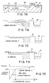
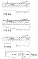
- 238000005421 electrostatic potential Methods 0.000 description 21
- 238000000034 method Methods 0.000 description 17
- 238000010586 diagram Methods 0.000 description 15
- 239000007943 implant Substances 0.000 description 14
- 238000012546 transfer Methods 0.000 description 13
- 230000008901 benefit Effects 0.000 description 9
- 230000008569 process Effects 0.000 description 9
- 238000009792 diffusion process Methods 0.000 description 8
- 239000000758 substrate Substances 0.000 description 8
- 230000000694 effects Effects 0.000 description 6
- 230000005684 electric field Effects 0.000 description 6
- 230000035945 sensitivity Effects 0.000 description 5
- 238000005286 illumination Methods 0.000 description 4
- 238000013461 design Methods 0.000 description 3
- 238000003384 imaging method Methods 0.000 description 3
- 229910021420 polycrystalline silicon Inorganic materials 0.000 description 3
- 229920005591 polysilicon Polymers 0.000 description 3
- 230000004888 barrier function Effects 0.000 description 2
- 230000008030 elimination Effects 0.000 description 2
- 238000003379 elimination reaction Methods 0.000 description 2
- 239000002184 metal Substances 0.000 description 2
- 238000012545 processing Methods 0.000 description 2
- 238000005215 recombination Methods 0.000 description 2
- 230000006798 recombination Effects 0.000 description 2
- 230000001629 suppression Effects 0.000 description 2
- 238000010521 absorption reaction Methods 0.000 description 1
- 230000002411 adverse Effects 0.000 description 1
- 230000003321 amplification Effects 0.000 description 1
- 238000004458 analytical method Methods 0.000 description 1
- 238000013459 approach Methods 0.000 description 1
- 238000006243 chemical reaction Methods 0.000 description 1
- 230000005574 cross-species transmission Effects 0.000 description 1
- 230000007812 deficiency Effects 0.000 description 1
- 230000000593 degrading effect Effects 0.000 description 1
- 230000006872 improvement Effects 0.000 description 1
- 230000010354 integration Effects 0.000 description 1
- 239000000463 material Substances 0.000 description 1
- 238000012986 modification Methods 0.000 description 1
- 230000004048 modification Effects 0.000 description 1
- 238000003199 nucleic acid amplification method Methods 0.000 description 1
- 238000012552 review Methods 0.000 description 1
- SBEQWOXEGHQIMW-UHFFFAOYSA-N silicon Chemical compound [Si].[Si] SBEQWOXEGHQIMW-UHFFFAOYSA-N 0.000 description 1
Images


Classifications
-
- H—ELECTRICITY
- H01—ELECTRIC ELEMENTS
- H01L—SEMICONDUCTOR DEVICES NOT COVERED BY CLASS H10
- H01L27/00—Devices consisting of a plurality of semiconductor or other solid-state components formed in or on a common substrate
- H01L27/14—Devices consisting of a plurality of semiconductor or other solid-state components formed in or on a common substrate including semiconductor components sensitive to infrared radiation, light, electromagnetic radiation of shorter wavelength or corpuscular radiation and specially adapted either for the conversion of the energy of such radiation into electrical energy or for the control of electrical energy by such radiation
- H01L27/144—Devices controlled by radiation
- H01L27/146—Imager structures
- H01L27/14683—Processes or apparatus peculiar to the manufacture or treatment of these devices or parts thereof
- H01L27/14689—MOS based technologies
-
- H—ELECTRICITY
- H01—ELECTRIC ELEMENTS
- H01L—SEMICONDUCTOR DEVICES NOT COVERED BY CLASS H10
- H01L27/00—Devices consisting of a plurality of semiconductor or other solid-state components formed in or on a common substrate
- H01L27/14—Devices consisting of a plurality of semiconductor or other solid-state components formed in or on a common substrate including semiconductor components sensitive to infrared radiation, light, electromagnetic radiation of shorter wavelength or corpuscular radiation and specially adapted either for the conversion of the energy of such radiation into electrical energy or for the control of electrical energy by such radiation
- H01L27/144—Devices controlled by radiation
- H01L27/146—Imager structures
- H01L27/14601—Structural or functional details thereof
- H01L27/14609—Pixel-elements with integrated switching, control, storage or amplification elements
-
- H—ELECTRICITY
- H01—ELECTRIC ELEMENTS
- H01L—SEMICONDUCTOR DEVICES NOT COVERED BY CLASS H10
- H01L27/00—Devices consisting of a plurality of semiconductor or other solid-state components formed in or on a common substrate
- H01L27/14—Devices consisting of a plurality of semiconductor or other solid-state components formed in or on a common substrate including semiconductor components sensitive to infrared radiation, light, electromagnetic radiation of shorter wavelength or corpuscular radiation and specially adapted either for the conversion of the energy of such radiation into electrical energy or for the control of electrical energy by such radiation
- H01L27/144—Devices controlled by radiation
- H01L27/146—Imager structures
- H01L27/14643—Photodiode arrays; MOS imagers
- H01L27/14654—Blooming suppression
-
- H—ELECTRICITY
- H01—ELECTRIC ELEMENTS
- H01L—SEMICONDUCTOR DEVICES NOT COVERED BY CLASS H10
- H01L27/00—Devices consisting of a plurality of semiconductor or other solid-state components formed in or on a common substrate
- H01L27/14—Devices consisting of a plurality of semiconductor or other solid-state components formed in or on a common substrate including semiconductor components sensitive to infrared radiation, light, electromagnetic radiation of shorter wavelength or corpuscular radiation and specially adapted either for the conversion of the energy of such radiation into electrical energy or for the control of electrical energy by such radiation
- H01L27/144—Devices controlled by radiation
- H01L27/146—Imager structures
- H01L27/14601—Structural or functional details thereof
- H01L27/14603—Special geometry or disposition of pixel-elements, address-lines or gate-electrodes
-
- Y—GENERAL TAGGING OF NEW TECHNOLOGICAL DEVELOPMENTS; GENERAL TAGGING OF CROSS-SECTIONAL TECHNOLOGIES SPANNING OVER SEVERAL SECTIONS OF THE IPC; TECHNICAL SUBJECTS COVERED BY FORMER USPC CROSS-REFERENCE ART COLLECTIONS [XRACs] AND DIGESTS
- Y02—TECHNOLOGIES OR APPLICATIONS FOR MITIGATION OR ADAPTATION AGAINST CLIMATE CHANGE
- Y02E—REDUCTION OF GREENHOUSE GAS [GHG] EMISSIONS, RELATED TO ENERGY GENERATION, TRANSMISSION OR DISTRIBUTION
- Y02E10/00—Energy generation through renewable energy sources
- Y02E10/50—Photovoltaic [PV] energy
- Y02E10/547—Monocrystalline silicon PV cells
Abstract
Description
- 5
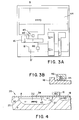
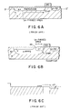
- prior art pixel
- 10
- pinned photodiode
- 12
- transfer gate
- 14
- floating diffusion
- 16
- reset gate
- 18
- reset drain
- 19
- surface of substrate
- 20
- substrate
- 22
- lightly doped n-type region
- 24
- p-type pinning layer
- 30
- photodiode
- 32
- n-type implant for photodiode
- 34
- p-type pinning layer for partially pinned photodiode
- 35
- pixel of the present invention
- 37
- n-type floating region
- 44
- pinned region of partially pinned photodiode
- 45
- unpinned region of partially pinned photodiode
- 46
- contact
- 50
- passive pixel sensor
- 54
- pinned region
- 55
- unpinned region
- 57
- select gate
- 59
- drain
Claims (10)
- An image sensor having at least one pixel comprising:a semiconductor of a first conductivity type within the sensor, the semiconductor being formed on a surface of the sensor;at least one photodiode formed, within the semiconductor near the surface, the photodiode being formed from a second conductivity type opposite the first conductivity type;a pinning layer formed on the surface over at least a portion of the photodiode creating a pinned photodiode region, the pinning layer being formed from the first conductivity type;an unpinned region formed within the photodiode near the surface in an area outside the portion used to form the pinning layer; anda sensing node coupled to the unpinned region interfacing the photodiode to external circuitry.
- The image sensor of claim 1 further comprising a control circuit operatively coupled to the pixel.
- The image sensor of claim 1 further comprising reset means for removing charge from the photodiode portion to a drain area.
- The image sensor of claim 1 wherein the unpinned region is formed having a layer of the second conductivity type at the surface.
- The image sensor of claim 1 wherein the sensor is an active pixel sensor and the unpinned region is a floating region that functions as a capacitor that is operatively coupled to a transistor.
- The image sensor of claim 5 wherein the transistor is operatively coupled to CMOS control circuitry.
- The image sensor of claim 1 wherein the pinned photodiode region further comprises a gradient dopant level formed to create an electrostatic gradient capable of pushing electrons towards the unpinned region.
- The image sensor of claim 1 further comprising utilization means for facilitating dynamic range compression operation of the sensor.
- The image sensor of claim 1 wherein the control circuitry is selected from one of either CMOS, PMOS, NMOS.
- A method of making an image sensor comprising the steps of:firstly providing a semiconductor having a first conductivity type within the sensor, such that the semiconductor is formed on a surface of the sensor;secondly providing at least one photodiode within the semiconductor near the surface from a second conductivity type opposite the first conductivity type;thirdly providing a pinning layer from the first conductivity type formed on the surface over at least a portion of the photodiode creating a pinned photodiode region;fourthly providing an unpinned region within the photodiode outside the portion on the surface used to form the pinning layer such that the unpinned region is formed near the surface and is coupled to a sensing node interfacing the photodiode to external circuitry
Applications Claiming Priority (2)
| Application Number | Priority Date | Filing Date | Title |
|---|---|---|---|
| US08/785,555 US5903021A (en) | 1997-01-17 | 1997-01-17 | Partially pinned photodiode for solid state image sensors |
| US785555 | 1997-01-17 |
Publications (3)
| Publication Number | Publication Date |
|---|---|
| EP0854516A2 true EP0854516A2 (en) | 1998-07-22 |
| EP0854516A3 EP0854516A3 (en) | 1998-10-07 |
| EP0854516B1 EP0854516B1 (en) | 2010-11-17 |
Family
ID=25135878
Family Applications (1)
| Application Number | Title | Priority Date | Filing Date |
|---|---|---|---|
| EP98200030A Expired - Lifetime EP0854516B1 (en) | 1997-01-17 | 1998-01-08 | Partially pinned photodiode for solid state image sensors |
Country Status (4)
| Country | Link |
|---|---|
| US (2) | US5903021A (en) |
| EP (1) | EP0854516B1 (en) |
| JP (1) | JPH10209422A (en) |
| DE (1) | DE69841998D1 (en) |
Cited By (19)
| Publication number | Priority date | Publication date | Assignee | Title |
|---|---|---|---|---|
| WO1999066560A1 (en) * | 1998-06-17 | 1999-12-23 | Foveon, Inc. | Storage pixel sensor and pixel sensor array with signal compression |
| GB2339333A (en) * | 1998-06-29 | 2000-01-19 | Hyundai Electronics Ind | Photodiode having charge transfer function and image sensor using the same. |
| EP1026748A1 (en) * | 1999-02-05 | 2000-08-09 | Omnivision Technologies Inc. | Improved active pixel with a pinned photodiode and method of making same |
| EP1032049A2 (en) | 1999-02-25 | 2000-08-30 | Canon Kabushiki Kaisha | Light-receiving element and photoelectric conversion device |
| EP1119188A2 (en) * | 2000-01-18 | 2001-07-25 | Eastman Kodak Company | Cmos active pixel image sensor with extended dynamic range and sensitivity |
| US6410899B1 (en) | 1998-06-17 | 2002-06-25 | Foveon, Inc. | Active pixel sensor with bootstrap amplification and reduced leakage during readout |
| EP1223623A2 (en) * | 2001-01-15 | 2002-07-17 | Sony Corporation | Solid-state image pickup device and driving method therefor |
| EP1231642A1 (en) * | 2001-02-12 | 2002-08-14 | STMicroelectronics S.A. | Three-transistor photodetector |
| FR2820883A1 (en) * | 2001-02-12 | 2002-08-16 | St Microelectronics Sa | HIGH CAPACITY PHOTODIODE |
| FR2824665A1 (en) * | 2001-05-09 | 2002-11-15 | St Microelectronics Sa | CMOS TYPE PHOTODETECTOR |
| US6566697B1 (en) | 2000-11-28 | 2003-05-20 | Dalsa, Inc. | Pinned photodiode five transistor pixel |
| US6697114B1 (en) | 1999-08-13 | 2004-02-24 | Foveon, Inc. | Triple slope pixel sensor and arry |
| US6713796B1 (en) | 2001-01-19 | 2004-03-30 | Dalsa, Inc. | Isolated photodiode |
| US6760070B1 (en) | 2000-02-29 | 2004-07-06 | Foveon, Inc. | High-sensitivity storage pixel sensor array having auto-exposure detection |
| EP1465258A1 (en) * | 2003-02-21 | 2004-10-06 | STMicroelectronics Limited | CMOS image sensors |
| US6809768B1 (en) | 2000-02-14 | 2004-10-26 | Foveon, Inc. | Double slope pixel sensor and array |
| US6940551B2 (en) | 2000-09-25 | 2005-09-06 | Foveon, Inc. | Active pixel sensor with noise cancellation |
| WO2009067372A1 (en) * | 2007-11-20 | 2009-05-28 | Aptina Imaging Corporation | Method and apparatus for controlling anti-blooming timing to reduce effects of dark current |
| US8120682B2 (en) | 1998-11-02 | 2012-02-21 | Canon Kabushiki Kaisha | Solid-state image pickup device and method of resetting the same |
Families Citing this family (97)
| Publication number | Priority date | Publication date | Assignee | Title |
|---|---|---|---|---|
| US5625210A (en) * | 1995-04-13 | 1997-04-29 | Eastman Kodak Company | Active pixel sensor integrated with a pinned photodiode |
| US6815791B1 (en) | 1997-02-10 | 2004-11-09 | Fillfactory | Buried, fully depletable, high fill factor photodiodes |
| US7199410B2 (en) * | 1999-12-14 | 2007-04-03 | Cypress Semiconductor Corporation (Belgium) Bvba | Pixel structure with improved charge transfer |
| JPH10270742A (en) * | 1997-03-28 | 1998-10-09 | Rohm Co Ltd | Photodiode |
| US6026964A (en) * | 1997-08-25 | 2000-02-22 | International Business Machines Corporation | Active pixel sensor cell and method of using |
| JPH11126893A (en) | 1997-10-23 | 1999-05-11 | Nikon Corp | Solid-state image-pickup element and manufacture thereof |
| US6714239B2 (en) * | 1997-10-29 | 2004-03-30 | Eastman Kodak Company | Active pixel sensor with programmable color balance |
| US6127697A (en) * | 1997-11-14 | 2000-10-03 | Eastman Kodak Company | CMOS image sensor |
| JP3874135B2 (en) * | 1997-12-05 | 2007-01-31 | 株式会社ニコン | Solid-state image sensor |
| NL1011381C2 (en) * | 1998-02-28 | 2000-02-15 | Hyundai Electronics Ind | Photodiode for a CMOS image sensor and method for its manufacture. |
| JPH11264761A (en) * | 1998-03-18 | 1999-09-28 | Honda Motor Co Ltd | Optical sensor circuit and image sensor using the same |
| TW425563B (en) * | 1998-06-03 | 2001-03-11 | Nippon Electric Co | Solid state image pickup device and driving method therefore |
| US6259145B1 (en) * | 1998-06-17 | 2001-07-10 | Intel Corporation | Reduced leakage trench isolation |
| FR2781929B1 (en) * | 1998-07-28 | 2002-08-30 | St Microelectronics Sa | IMAGE SENSOR WITH PHOTODIODE ARRAY |
| US6259124B1 (en) * | 1998-08-07 | 2001-07-10 | Eastman Kodak Company | Active pixel sensor with high fill factor blooming protection |
| US6677628B2 (en) * | 1998-09-17 | 2004-01-13 | Micron Technology, Inc. | Pinned floating photoreceptor with active pixel sensor |
| US6207984B1 (en) * | 1998-12-23 | 2001-03-27 | United Microelectronics Corp. | CMOS sensor |
| US20030089929A1 (en) * | 2001-02-14 | 2003-05-15 | Rhodes Howard E. | Trench photosensor for a CMOS imager |
| US6232626B1 (en) * | 1999-02-01 | 2001-05-15 | Micron Technology, Inc. | Trench photosensor for a CMOS imager |
| US6388243B1 (en) | 1999-03-01 | 2002-05-14 | Photobit Corporation | Active pixel sensor with fully-depleted buried photoreceptor |
| JP3576033B2 (en) * | 1999-03-31 | 2004-10-13 | 株式会社東芝 | Solid-state imaging device |
| US6476426B1 (en) * | 1999-07-06 | 2002-11-05 | Motorola, Inc. | Electronic component and method for improving pixel charge transfer in the electronic component |
| US6300219B1 (en) | 1999-08-30 | 2001-10-09 | Micron Technology, Inc. | Method of forming trench isolation regions |
| US6090639A (en) * | 1999-09-08 | 2000-07-18 | United Microelectronics Corp. | Method for forming a photo diode and a CMOS transistor simultaneously |
| US6271553B1 (en) * | 1999-11-29 | 2001-08-07 | United Microelectronics Corp. | Photo sensor in a photo diode |
| JP4419238B2 (en) * | 1999-12-27 | 2010-02-24 | ソニー株式会社 | Solid-state imaging device and manufacturing method thereof |
| US6372537B1 (en) * | 2000-03-17 | 2002-04-16 | Taiwan Semiconductor Manufacturing Company | Pinned photodiode structure in a 3T active pixel sensor |
| US6518085B1 (en) * | 2000-08-09 | 2003-02-11 | Taiwan Semiconductor Manufacturing Company | Method for making spectrally efficient photodiode structures for CMOS color imagers |
| US6448596B1 (en) * | 2000-08-15 | 2002-09-10 | Innotech Corporation | Solid-state imaging device |
| US6365926B1 (en) * | 2000-09-20 | 2002-04-02 | Eastman Kodak Company | CMOS active pixel with scavenging diode |
| JP2002151729A (en) * | 2000-11-13 | 2002-05-24 | Sony Corp | Semiconductor device and its manufacturing method |
| US6504195B2 (en) * | 2000-12-29 | 2003-01-07 | Eastman Kodak Company | Alternate method for photodiode formation in CMOS image sensors |
| JP4130307B2 (en) * | 2001-01-15 | 2008-08-06 | Necエレクトロニクス株式会社 | Solid-state imaging device |
| US7180798B2 (en) * | 2001-04-12 | 2007-02-20 | Fuji Electric Co., Ltd. | Semiconductor physical quantity sensing device |
| KR100381026B1 (en) * | 2001-05-22 | 2003-04-23 | 주식회사 하이닉스반도체 | CMOS Image sensor capable of increasing punch through voltage and charge integration of photodiode and method for forming the same |
| JP2003060192A (en) * | 2001-08-20 | 2003-02-28 | Sony Corp | Method for manufacturing solid-state image pickup device |
| US6881986B1 (en) | 2001-11-07 | 2005-04-19 | Taiwan Semiconductor Manufacturing Company | Design and fabrication method for finger n-type doped photodiodes with high sensitivity for CIS products |
| FR2833408B1 (en) * | 2001-12-12 | 2004-03-12 | St Microelectronics Sa | METHOD FOR CONTROLLING THE ILLUMINATION OF A PHOTODIODE AND CORRESPONDING INTEGRATED CIRCUIT |
| JP2003258231A (en) * | 2002-03-05 | 2003-09-12 | Sony Corp | Solid-state image sensor |
| KR20030096659A (en) * | 2002-06-17 | 2003-12-31 | 삼성전자주식회사 | Pixel array region of an image sensor, structure thereof and fabrication method thereof |
| US6781171B2 (en) * | 2002-07-19 | 2004-08-24 | Dongbu Electronics Co., Ltd. | Pinned photodiode for a CMOS image sensor and fabricating method thereof |
| US6744084B2 (en) * | 2002-08-29 | 2004-06-01 | Micro Technology, Inc. | Two-transistor pixel with buried reset channel and method of formation |
| CN100468753C (en) * | 2002-08-30 | 2009-03-11 | 皇家飞利浦电子股份有限公司 | Image sensor, camera system comprising the image sensor and method of manufacturing such a device |
| US6586789B1 (en) * | 2002-10-07 | 2003-07-01 | Lixin Zhao | Pixel image sensor |
| US7087944B2 (en) * | 2003-01-16 | 2006-08-08 | Micron Technology, Inc. | Image sensor having a charge storage region provided within an implant region |
| KR20040093786A (en) * | 2003-04-30 | 2004-11-09 | 매그나칩 반도체 유한회사 | Method of manufacturing cmos image sensor |
| US7009227B2 (en) * | 2003-06-16 | 2006-03-07 | Micron Technology, Inc. | Photodiode structure and image pixel structure |
| FR2857158B1 (en) * | 2003-07-01 | 2006-04-28 | St Microelectronics Sa | METHOD FOR CONTROLLING A MOS TYPE PHOTOCOPIER |
| US6900484B2 (en) * | 2003-07-30 | 2005-05-31 | Micron Technology, Inc. | Angled pinned photodiode for high quantum efficiency |
| US7115855B2 (en) * | 2003-09-05 | 2006-10-03 | Micron Technology, Inc. | Image sensor having pinned floating diffusion diode |
| US7541627B2 (en) * | 2004-03-08 | 2009-06-02 | Foveon, Inc. | Method and apparatus for improving sensitivity in vertical color CMOS image sensors |
| US7238977B2 (en) * | 2004-08-19 | 2007-07-03 | Micron Technology, Inc. | Wide dynamic range sensor having a pinned diode with multiple pinned voltages |
| US7492404B2 (en) * | 2004-08-27 | 2009-02-17 | Eastman Kodak Company | Fast flush structure for solid-state image sensors |
| JP4756839B2 (en) * | 2004-09-01 | 2011-08-24 | キヤノン株式会社 | Solid-state imaging device and camera |
| KR100614650B1 (en) * | 2004-09-16 | 2006-08-22 | 삼성전자주식회사 | Image sensor and method for forming the same |
| JP4613305B2 (en) | 2004-10-19 | 2011-01-19 | 国立大学法人静岡大学 | Imaging device with embedded photodiode structure |
| KR20060058573A (en) * | 2004-11-25 | 2006-05-30 | 한국전자통신연구원 | Cmos image sensor |
| JP4725095B2 (en) | 2004-12-15 | 2011-07-13 | ソニー株式会社 | Back-illuminated solid-state imaging device and manufacturing method thereof |
| KR100654342B1 (en) * | 2005-02-07 | 2006-12-08 | 삼성전자주식회사 | image sensor |
| US7701493B2 (en) * | 2005-02-28 | 2010-04-20 | Micron Technology, Inc. | Imager row-wise noise correction |
| WO2006103733A1 (en) | 2005-03-28 | 2006-10-05 | Fujitsu Limited | Image pickup device |
| US7750958B1 (en) | 2005-03-28 | 2010-07-06 | Cypress Semiconductor Corporation | Pixel structure |
| US7808022B1 (en) | 2005-03-28 | 2010-10-05 | Cypress Semiconductor Corporation | Cross talk reduction |
| TWI266429B (en) * | 2005-05-05 | 2006-11-11 | Pixart Imaging Inc | Pinned photodiode sensor with gate controlled SCR transfer switch and method of formation |
| US20070023803A1 (en) * | 2005-07-26 | 2007-02-01 | Dongbu Electronics Co., Ltd. | CMOS image sensor and method of fabricating the same |
| KR100752182B1 (en) * | 2005-10-12 | 2007-08-24 | 동부일렉트로닉스 주식회사 | CMOS image sensor and method for manufacturing the same |
| US7682977B2 (en) * | 2006-05-11 | 2010-03-23 | Micron Technology, Inc. | Methods of forming trench isolation and methods of forming arrays of FLASH memory cells |
| KR100738516B1 (en) * | 2006-05-25 | 2007-07-11 | (주) 픽셀플러스 | Active pixel having pinned photodiode with coupling capacitor and method for sensing a signal thereof |
| KR100790587B1 (en) * | 2006-05-25 | 2008-01-02 | (주) 픽셀플러스 | Image sensor pixel having pinned photodiode with coupling capacitor and method for sensing a signal thereof |
| US7675093B2 (en) | 2006-11-28 | 2010-03-09 | Micron Technology, Inc. | Antiblooming imaging apparatus, system, and methods |
| US8304821B2 (en) * | 2006-12-23 | 2012-11-06 | Semiconductor Manufacturing International (Shanghai) Corporation | CMOS image sensor |
| JP5584982B2 (en) | 2009-02-09 | 2014-09-10 | ソニー株式会社 | Solid-state imaging device and camera system |
| US7724293B2 (en) * | 2007-03-12 | 2010-05-25 | Aptina Imaging Corporation | Multi-purpose image sensor circuits, imager, system and method of operation |
| US7915702B2 (en) | 2007-03-15 | 2011-03-29 | Eastman Kodak Company | Reduced pixel area image sensor |
| US7834411B2 (en) * | 2007-05-15 | 2010-11-16 | Foveon, Inc. | CMOS pixel sensor with depleted photocollectors and a depleted common node |
| CN101459184B (en) * | 2007-12-13 | 2011-03-23 | 中芯国际集成电路制造(上海)有限公司 | System and method for sensing image on CMOS |
| CN101625996B (en) * | 2008-07-08 | 2011-03-23 | 中芯国际集成电路制造(上海)有限公司 | ONO side wall etching process for reducing dark current |
| CN101630659B (en) * | 2008-07-15 | 2012-05-23 | 中芯国际集成电路制造(上海)有限公司 | Method for forming CMOS image sensor by using tri-gate process and structure of CMOS image sensor using tri-gate process |
| JP5283216B2 (en) * | 2008-07-31 | 2013-09-04 | 国立大学法人静岡大学 | High-speed charge transfer photodiode, lock-in pixel and solid-state imaging device |
| US8476567B2 (en) | 2008-09-22 | 2013-07-02 | Semiconductor Components Industries, Llc | Active pixel with precharging circuit |
| US8329499B2 (en) * | 2008-12-10 | 2012-12-11 | Truesense Imaging, Inc. | Method of forming lateral overflow drain and channel stop regions in image sensors |
| US8338248B2 (en) * | 2008-12-25 | 2012-12-25 | National University Corporation Shizuoka University | Semiconductor element and solid-state imaging device |
| JP5493430B2 (en) * | 2009-03-31 | 2014-05-14 | ソニー株式会社 | SOLID-STATE IMAGING DEVICE, ITS MANUFACTURING METHOD, AND ELECTRONIC DEVICE |
| DE102009020218B8 (en) * | 2009-05-07 | 2011-05-12 | Fraunhofer-Gesellschaft zur Förderung der angewandten Forschung e.V. | Detector and method for detecting electromagnetic radiation and computer program for carrying out the method |
| EP2487897B1 (en) * | 2009-10-05 | 2016-09-14 | National University Corporation Shizuoka University | Semiconductor element and solid-state imaging device |
| US8907388B2 (en) | 2010-02-05 | 2014-12-09 | National University Corporation Shizuoka University | Optical-information acquiring element, optical information acquiring element array, and hybrid solid-state imaging device |
| US8878264B2 (en) * | 2011-04-26 | 2014-11-04 | Aptina Imaging Corporation | Global shutter pixel with improved efficiency |
| DE102011076635B3 (en) * | 2011-05-27 | 2012-10-18 | Fraunhofer-Gesellschaft zur Förderung der angewandten Forschung e.V. | Photodetector i.e. lateral drift field photodetector, for detecting electromagnetic radiation, has bus control electrode arranged in region of trough adjacent to connection doping regions, transfer control electrodes and detection region |
| FR2986906B1 (en) | 2012-02-15 | 2015-06-19 | New Imaging Technologies Sas | IMPROVED LOAD TRANSFER ACTIVE PIXEL STRUCTURE |
| JP6077786B2 (en) | 2012-08-22 | 2017-02-08 | キヤノン株式会社 | Imaging device |
| FR2997596B1 (en) | 2012-10-26 | 2015-12-04 | New Imaging Technologies Sas | STRUCTURE OF A CMOS ACTIVE PIXEL |
| US9348035B2 (en) | 2013-10-22 | 2016-05-24 | General Electric Company | Systems and methods for selectable detector configurations |
| US9526468B2 (en) | 2014-09-09 | 2016-12-27 | General Electric Company | Multiple frame acquisition for exposure control in X-ray medical imagers |
| TWI731026B (en) | 2016-01-15 | 2021-06-21 | 新加坡商海特根微光學公司 | Semiconductor devices |
| US10236400B2 (en) | 2016-02-01 | 2019-03-19 | Heptagon Micro Optics Pte. Ltd. | Quantum dot film based demodulation structures |
| EP3719840A4 (en) * | 2017-11-30 | 2021-02-24 | Panasonic Intellectual Property Management Co., Ltd. | Image capturing device |
| GB2574619B (en) | 2018-06-12 | 2022-10-12 | Res & Innovation Uk | Image sensor |
Citations (2)
| Publication number | Priority date | Publication date | Assignee | Title |
|---|---|---|---|---|
| US5262871A (en) | 1989-11-13 | 1993-11-16 | Rutgers, The State University | Multiple resolution image sensor |
| EP0738010A2 (en) | 1995-04-13 | 1996-10-16 | Eastman Kodak Company | Active pixel sensor integrated with a pinned photodiode |
Family Cites Families (27)
| Publication number | Priority date | Publication date | Assignee | Title |
|---|---|---|---|---|
| JPS5651165A (en) * | 1979-10-03 | 1981-05-08 | Hitachi Ltd | Noise eliminating circuit |
| US4484210A (en) * | 1980-09-05 | 1984-11-20 | Nippon Electric Co., Ltd. | Solid-state imaging device having a reduced image lag |
| JPS57121374A (en) * | 1981-01-21 | 1982-07-28 | Hitachi Ltd | Solid image pickup device |
| JPH0714044B2 (en) * | 1984-11-22 | 1995-02-15 | 株式会社日立製作所 | Charge coupled device input circuit |
| JPS62160750A (en) * | 1986-01-10 | 1987-07-16 | Hitachi Ltd | Substrate-voltage generating circuit |
| JPS63100879A (en) * | 1986-10-17 | 1988-05-02 | Hitachi Ltd | Solid-state image pickup device |
| JPS63299268A (en) * | 1987-05-29 | 1988-12-06 | Toshiba Corp | Solid-state image sensing device |
| JPH01135184A (en) * | 1987-11-19 | 1989-05-26 | Nec Corp | Solid-state image pickup element |
| US4984047A (en) * | 1988-03-21 | 1991-01-08 | Eastman Kodak Company | Solid-state image sensor |
| US4908518A (en) * | 1989-02-10 | 1990-03-13 | Eastman Kodak Company | Interline transfer CCD image sensing device with electrode structure for each pixel |
| US5115458A (en) * | 1989-09-05 | 1992-05-19 | Eastman Kodak Company | Reducing dark current in charge coupled devices |
| US5051797A (en) * | 1989-09-05 | 1991-09-24 | Eastman Kodak Company | Charge-coupled device (CCD) imager and method of operation |
| US5182623A (en) * | 1989-11-13 | 1993-01-26 | Texas Instruments Incorporated | Charge coupled device/charge super sweep image system and method for making |
| JPH07105458B2 (en) * | 1989-11-21 | 1995-11-13 | 株式会社東芝 | Composite integrated circuit device |
| US5235198A (en) * | 1989-11-29 | 1993-08-10 | Eastman Kodak Company | Non-interlaced interline transfer CCD image sensing device with simplified electrode structure for each pixel |
| US5060245A (en) * | 1990-06-29 | 1991-10-22 | The United States Of America As Represented By The Secretary Of The Air Force | Interline transfer CCD image sensing apparatus |
| JP3125303B2 (en) * | 1990-11-26 | 2001-01-15 | 日本電気株式会社 | Solid-state imaging device |
| US5256891A (en) * | 1991-06-07 | 1993-10-26 | Eastman Kodak Company | CCD electrode structure for image sensors |
| KR100298039B1 (en) * | 1991-07-11 | 2001-10-24 | 윌리엄 비. 켐플러 | Charge multiplication device and manufacturing method |
| JPH05251684A (en) * | 1991-11-25 | 1993-09-28 | Eastman Kodak Co | Ccd image sensor having improved bloom prevention characteristic |
| JPH05283666A (en) * | 1992-03-30 | 1993-10-29 | Sony Corp | Solid state image pickup |
| KR960002645B1 (en) * | 1992-04-03 | 1996-02-24 | 엘지반도체주식회사 | Charge transferring device and solid state image picking-up device |
| US5235196A (en) * | 1992-07-24 | 1993-08-10 | Eastman Kodak Company | Transfer region design for charge-coupled device image sensor |
| JPH07161958A (en) * | 1993-12-09 | 1995-06-23 | Nec Corp | Solid-state image pick up device |
| US5471515A (en) * | 1994-01-28 | 1995-11-28 | California Institute Of Technology | Active pixel sensor with intra-pixel charge transfer |
| KR0136934B1 (en) * | 1994-02-23 | 1998-04-24 | 문정환 | Linear ccd solid image sensor |
| US5514886A (en) * | 1995-01-18 | 1996-05-07 | Eastman Kodak Company | Image sensor with improved output region for superior charge transfer characteristics |
-
1997
- 1997-01-17 US US08/785,555 patent/US5903021A/en not_active Expired - Lifetime
-
1998
- 1998-01-08 EP EP98200030A patent/EP0854516B1/en not_active Expired - Lifetime
- 1998-01-08 DE DE69841998T patent/DE69841998D1/en not_active Expired - Lifetime
- 1998-01-16 JP JP10007072A patent/JPH10209422A/en active Pending
- 1998-10-01 US US09/164,968 patent/US6051447A/en not_active Expired - Lifetime
Patent Citations (2)
| Publication number | Priority date | Publication date | Assignee | Title |
|---|---|---|---|---|
| US5262871A (en) | 1989-11-13 | 1993-11-16 | Rutgers, The State University | Multiple resolution image sensor |
| EP0738010A2 (en) | 1995-04-13 | 1996-10-16 | Eastman Kodak Company | Active pixel sensor integrated with a pinned photodiode |
Cited By (33)
| Publication number | Priority date | Publication date | Assignee | Title |
|---|---|---|---|---|
| WO1999066560A1 (en) * | 1998-06-17 | 1999-12-23 | Foveon, Inc. | Storage pixel sensor and pixel sensor array with signal compression |
| US6410899B1 (en) | 1998-06-17 | 2002-06-25 | Foveon, Inc. | Active pixel sensor with bootstrap amplification and reduced leakage during readout |
| US6512544B1 (en) | 1998-06-17 | 2003-01-28 | Foveon, Inc. | Storage pixel sensor and array with compression |
| GB2339333A (en) * | 1998-06-29 | 2000-01-19 | Hyundai Electronics Ind | Photodiode having charge transfer function and image sensor using the same. |
| GB2339333B (en) * | 1998-06-29 | 2003-07-09 | Hyundai Electronics Ind | Photodiode having charge function and image sensor using the same |
| US9083901B2 (en) | 1998-11-02 | 2015-07-14 | Canon Kabushiki Kaisha | Solid-state image pickup device and method of resetting the same |
| EP0999698B1 (en) * | 1998-11-02 | 2013-06-19 | Canon Kabushiki Kaisha | Solid-state image pickup device and method of resetting the same |
| US8120682B2 (en) | 1998-11-02 | 2012-02-21 | Canon Kabushiki Kaisha | Solid-state image pickup device and method of resetting the same |
| EP1026748A1 (en) * | 1999-02-05 | 2000-08-09 | Omnivision Technologies Inc. | Improved active pixel with a pinned photodiode and method of making same |
| EP1032049A2 (en) | 1999-02-25 | 2000-08-30 | Canon Kabushiki Kaisha | Light-receiving element and photoelectric conversion device |
| EP1032049B1 (en) * | 1999-02-25 | 2011-07-13 | Canon Kabushiki Kaisha | Photoelectric converting element |
| US6697114B1 (en) | 1999-08-13 | 2004-02-24 | Foveon, Inc. | Triple slope pixel sensor and arry |
| EP1119188A3 (en) * | 2000-01-18 | 2002-09-04 | Eastman Kodak Company | Cmos active pixel image sensor with extended dynamic range and sensitivity |
| EP1119188A2 (en) * | 2000-01-18 | 2001-07-25 | Eastman Kodak Company | Cmos active pixel image sensor with extended dynamic range and sensitivity |
| US6710804B1 (en) | 2000-01-18 | 2004-03-23 | Eastman Kodak Company | CMOS active pixel image sensor with extended dynamic range and sensitivity |
| US6809768B1 (en) | 2000-02-14 | 2004-10-26 | Foveon, Inc. | Double slope pixel sensor and array |
| US6760070B1 (en) | 2000-02-29 | 2004-07-06 | Foveon, Inc. | High-sensitivity storage pixel sensor array having auto-exposure detection |
| US6882367B1 (en) | 2000-02-29 | 2005-04-19 | Foveon, Inc. | High-sensitivity storage pixel sensor having auto-exposure detection |
| US6940551B2 (en) | 2000-09-25 | 2005-09-06 | Foveon, Inc. | Active pixel sensor with noise cancellation |
| US6566697B1 (en) | 2000-11-28 | 2003-05-20 | Dalsa, Inc. | Pinned photodiode five transistor pixel |
| US7259790B2 (en) | 2001-01-15 | 2007-08-21 | Sony Corporation | MOS type solid-state image pickup device and driving method comprised of a photodiode a detection portion and a transfer transistor |
| EP1223623A3 (en) * | 2001-01-15 | 2005-04-20 | Sony Corporation | Solid-state image pickup device and driving method therefor |
| US7518168B2 (en) | 2001-01-15 | 2009-04-14 | Sony Corporation | MOS type solid-state image pickup device and driving method comprised of a photodiode, a detection portion, and a transfer transistor |
| EP1223623A2 (en) * | 2001-01-15 | 2002-07-17 | Sony Corporation | Solid-state image pickup device and driving method therefor |
| US6713796B1 (en) | 2001-01-19 | 2004-03-30 | Dalsa, Inc. | Isolated photodiode |
| FR2820883A1 (en) * | 2001-02-12 | 2002-08-16 | St Microelectronics Sa | HIGH CAPACITY PHOTODIODE |
| FR2820882A1 (en) * | 2001-02-12 | 2002-08-16 | St Microelectronics Sa | THREE TRANSISTOR PHOTODETECTOR |
| EP1231642A1 (en) * | 2001-02-12 | 2002-08-14 | STMicroelectronics S.A. | Three-transistor photodetector |
| FR2824665A1 (en) * | 2001-05-09 | 2002-11-15 | St Microelectronics Sa | CMOS TYPE PHOTODETECTOR |
| EP1465258A1 (en) * | 2003-02-21 | 2004-10-06 | STMicroelectronics Limited | CMOS image sensors |
| WO2009067372A1 (en) * | 2007-11-20 | 2009-05-28 | Aptina Imaging Corporation | Method and apparatus for controlling anti-blooming timing to reduce effects of dark current |
| US7763837B2 (en) | 2007-11-20 | 2010-07-27 | Aptina Imaging Corporation | Method and apparatus for controlling anti-blooming timing to reduce effects of dark current |
| US7897904B2 (en) | 2007-11-20 | 2011-03-01 | Aptina Imaging Corporation | Method and apparatus for controlling anti-blooming timing to reduce effects of dark current |
Also Published As
| Publication number | Publication date |
|---|---|
| JPH10209422A (en) | 1998-08-07 |
| EP0854516A3 (en) | 1998-10-07 |
| US6051447A (en) | 2000-04-18 |
| US5903021A (en) | 1999-05-11 |
| EP0854516B1 (en) | 2010-11-17 |
| DE69841998D1 (en) | 2010-12-30 |
Similar Documents
| Publication | Publication Date | Title |
|---|---|---|
| US6051447A (en) | Partially pinned photodiode for solid state image sensors | |
| US6858460B2 (en) | Retrograde well structure for a CMOS imager | |
| US6180969B1 (en) | CMOS image sensor with equivalent potential diode | |
| EP1032049B1 (en) | Photoelectric converting element | |
| JP3645585B2 (en) | Charge coupled device type solid-state imaging device having overflow drain structure | |
| US9654713B2 (en) | Image sensors, methods, and pixels with tri-level biased transfer gates | |
| EP2030240B1 (en) | Pmos pixel structure with low cross talk | |
| USRE45357E1 (en) | Twin p-well CMOS imager | |
| US6815743B2 (en) | CMOS imager and method of formation | |
| US7166878B2 (en) | Image sensor with deep well region and method of fabricating the image sensor | |
| US6927089B2 (en) | CMOS imager and method of formation | |
| US20060151848A1 (en) | Photogate with improved short wavelength response for a CMOS imager | |
| US8508638B2 (en) | 3T pixel for CMOS image sensors with low reset noise and low dark current generation utilizing parametric reset | |
| EP1223746B1 (en) | Active pixel image sensor with improved linearity | |
| US6686220B2 (en) | Retrograde well structure for a CMOS imager | |
| KR100790224B1 (en) | Stratified photo-diode for high resolution cmos image sensors implemented in sti technology | |
| KR100864180B1 (en) | CMOS image sensor and image data processing method thereof | |
| KR100397665B1 (en) | Cmos active pixel for improving sensitivity |
Legal Events
| Date | Code | Title | Description |
|---|---|---|---|
| PUAI | Public reference made under article 153(3) epc to a published international application that has entered the european phase |
Free format text: ORIGINAL CODE: 0009012 |
|
| AK | Designated contracting states |
Kind code of ref document: A2 Designated state(s): DE FR GB |
|
| AX | Request for extension of the european patent |
Free format text: AL;LT;LV;MK;RO;SI |
|
| PUAL | Search report despatched |
Free format text: ORIGINAL CODE: 0009013 |
|
| AK | Designated contracting states |
Kind code of ref document: A3 Designated state(s): AT BE CH DE DK ES FI FR GB GR IE IT LI LU MC NL PT SE |
|
| 17P | Request for examination filed |
Effective date: 19990308 |
|
| AKX | Designation fees paid |
Free format text: DE FR GB |
|
| GRAP | Despatch of communication of intention to grant a patent |
Free format text: ORIGINAL CODE: EPIDOSNIGR1 |
|
| GRAS | Grant fee paid |
Free format text: ORIGINAL CODE: EPIDOSNIGR3 |
|
| GRAA | (expected) grant |
Free format text: ORIGINAL CODE: 0009210 |
|
| AK | Designated contracting states |
Kind code of ref document: B1 Designated state(s): DE FR GB |
|
| REG | Reference to a national code |
Ref country code: GB Ref legal event code: FG4D |
|
| REF | Corresponds to: |
Ref document number: 69841998 Country of ref document: DE Date of ref document: 20101230 Kind code of ref document: P |
|
| REG | Reference to a national code |
Ref country code: GB Ref legal event code: 732E Free format text: REGISTERED BETWEEN 20110704 AND 20110706 |
|
| RAP2 | Party data changed (patent owner data changed or rights of a patent transferred) |
Owner name: OMNIVISION TECHNOLOGIES, INC. |
|
| REG | Reference to a national code |
Ref country code: DE Ref legal event code: R082 Ref document number: 69841998 Country of ref document: DE Representative=s name: WAGNER & GEYER PARTNERSCHAFT MBB PATENT- UND R, DE Effective date: 20110729 Ref country code: DE Ref legal event code: R082 Ref document number: 69841998 Country of ref document: DE Representative=s name: WAGNER & GEYER PARTNERSCHAFT PATENT- UND RECHT, DE Effective date: 20110729 Ref country code: DE Ref legal event code: R081 Ref document number: 69841998 Country of ref document: DE Owner name: OMNIVISION TECHNOLOGIES, INC., US Free format text: FORMER OWNER: EASTMAN KODAK CO., ROCHESTER, US Effective date: 20110729 Ref country code: DE Ref legal event code: R081 Ref document number: 69841998 Country of ref document: DE Owner name: OMNIVISION TECHNOLOGIES, INC., SANTA CLARA, US Free format text: FORMER OWNER: EASTMAN KODAK CO., ROCHESTER, N.Y., US Effective date: 20110729 |
|
| PLBE | No opposition filed within time limit |
Free format text: ORIGINAL CODE: 0009261 |
|
| STAA | Information on the status of an ep patent application or granted ep patent |
Free format text: STATUS: NO OPPOSITION FILED WITHIN TIME LIMIT |
|
| REG | Reference to a national code |
Ref country code: FR Ref legal event code: TP Owner name: OMNI VISION TECHNOLOGIES, INC., US Effective date: 20110829 |
|
| 26N | No opposition filed |
Effective date: 20110818 |
|
| REG | Reference to a national code |
Ref country code: DE Ref legal event code: R097 Ref document number: 69841998 Country of ref document: DE Effective date: 20110818 |
|
| REG | Reference to a national code |
Ref country code: FR Ref legal event code: PLFP Year of fee payment: 19 |
|
| REG | Reference to a national code |
Ref country code: FR Ref legal event code: PLFP Year of fee payment: 20 |
|
| PGFP | Annual fee paid to national office [announced via postgrant information from national office to epo] |
Ref country code: GB Payment date: 20161228 Year of fee payment: 20 |
|
| PGFP | Annual fee paid to national office [announced via postgrant information from national office to epo] |
Ref country code: DE Payment date: 20170131 Year of fee payment: 20 Ref country code: FR Payment date: 20170103 Year of fee payment: 20 |
|
| REG | Reference to a national code |
Ref country code: DE Ref legal event code: R071 Ref document number: 69841998 Country of ref document: DE |
|
| REG | Reference to a national code |
Ref country code: GB Ref legal event code: PE20 Expiry date: 20180107 |
|
| PG25 | Lapsed in a contracting state [announced via postgrant information from national office to epo] |
Ref country code: GB Free format text: LAPSE BECAUSE OF EXPIRATION OF PROTECTION Effective date: 20180107 |