This is a Continuation-in-Part of U.S. Patent Application Serial No.
08/788,108 by Roberts et al., entitled
Making Color Filter Arrays By Transferring
Two Or More Colorants Simultaneously,
U.S. Patent Application Serial No.
08/788,532 by Roberts, et al., entitled
A Method Of Making A Color Filter Array By
Colorant Transfer And Etch,
, U.S. Patent Application Serial No. 08/787,732, and
entitled
Method of Making Color Filter Arrays By Colorant Transfer Using Chemical
Mechanical Polishing,
by Roberts, et al., and U.S. Patent Application Serial No.
08/789,590 by Roberts, et al., entitled
Making Color Filter Arrays By Transferring
Colorant Material.
The present invention is related to U.S. Patent Application Serial No.
08/648,772 filed May. 16, 1996 and entitled
Method of Forming an Organic
Electroluminescent Display Panel,
by Littman, et al. The disclosure of this related
application is incorporated herein by reference.
The present invention relates to methods of making color filter arrays
which are suitable for display applications such as liquid crystal displays or light
emitting diode displays and are particularly suitable for use on image sensors.
BACKGROUND OF THE INVENTION
In making color filter arrays, separate layers of different colors must be
formed. Frequently these layers are formed using dye as the colorant material which
is imbibed into dye receiving layers which must be of a controlled thickness, and a
precise amount of dye must be used to achieve the appropriate color. See, for
example, commonly assigned U.S. Patent No. 4,764,670 to Pace et al., U.S. Patent
No. 4,876,167 to Snow et al., and U.S. Patent No. 5,576,265 to DeBoer et al. which
describe such a process. An additional problem associated with this process is that the
dye receiving layers swell upon the introduction of dyes, limiting the smallest
dimension which can be attainable for use over very small filter elements. In addition,
the dyes spread within the dye receiving layer, resulting in loss in edge sharpness of
the filter elements. Another problem with this process is that dyes are susceptible to
fading on exposure to light.
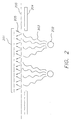
Turning to FIG. 1, which shows a method for making coatings from
evaporated organic colorants, a substrate 102 is positioned adjacent to an aperture
mask 104. The aperture mask provides an aperture over a portion of the substrate. An
organic colorant which is to provide the coating is placed into a source boat 100,
which is heated by passing an electric current through it. Alternatively, the boat may
be heated by the application of radiant heating from a suitably placed heat source.
Upon being heated under reduced pressure, the colorant vaporizes and travels from the
source, impinging on mask 105. The portion of colorant vapor which passes through
the opening in mask 105 travels along the lines 103, and between those lines,
depositing on the substrate 102 and mask 104.
There are a number of problems associated with this technique which
involves depositing layers in a partial vacuum and is frequently referred to in the art as
physical vapor deposition (PVD). In certain cases, it is difficult to control the
thickness and uniformity of the colorant deposited on the substrate. The process of
vacuum deposition of the colorant typically requires the use of an appropriate
placement of sources or masks or moving substrate fixtures to produce a coating
which is uniform. However, the colorant material may deposit on the mask and
vacuum fixtures to such a degree that it flakes off, creating undesirable contamination
and waste of the colorant, and requiring frequent clean-up. In addition, the moving
fixtures may generate undesirable particulate materials which may cause
contamination of the substrate.
Some other problems in making color filter arrays by the PVD process
are the need to use a large source-to-substrate spacing which requires large chambers
and large pumps to reach a sufficient vacuum, and the need for masks which cause
low-material utilization and build-up on the mask with the concomitant contamination
problems. Very specific off-axis source location relative to the substrate, which is
sometimes needed for uniform coating, causes very poor material utilization. Still
further, source replenishment problems exist for coating multiple substrates in one
pump-down. In addition, when multiple layers are deposited, the process needs to be
carefully monitored for the thickness of layers in the multiple colorant coatings in
multiple cycles.
SUMMARY OF THE INVENTION
It is an object of the present invention to provide an improved method
for making color filter arrays which obviates the above difficulties, provides uniform
colorant over the substrate, and is of low cost and high quality.
The present invention provides in one embodiment a method of
making a color filter array on a first substrate comprising the steps of:
In another embodiment, the present invention provides a method of
making a color filter array on a first substrate comprising the steps of:
In yet another embodiment the present invention provides a method of
making a color filter array on a first substrate comprising the steps of:
Still another embodiment of the present invention provides a method of
making a color filter array on a first substrate comprising the steps of:
Advantages
Advantages of this technique include the ability to form colorant layers
with tuned colors by co-deposition of a plurality of colorant materials in a single step,
along with the ability to pattern the colorant layers to form an array of colorant
elements. In addition, it provides for an evaporative purification of the colorant
during the preparation of the transferable colorant coating and the effective utilization
of evaporant materials with high quality uniformity over a large areas. Other
advantages include precise control of layer thickness, lower maintenance of deposition
vacuum chambers, and minimal monitoring for the deposition process. Still further, it
offers the ability to coat at higher pressures and in smaller vacuum chambers which
permit faster cycle time and the use of lower-cost vacuum equipment than for standard
PVD techniques.
BRIEF DESCRIPTION OF THE DRAWINGS
FIG. 1 shows a typical configuration for conventional physical vapor
deposition (PVD).
FIG. 2 shows a typical configuration for the thermal transfer of a
material from an intermediate substrate to the final substrate, according to the present
invention.
FIGS. 3A-H show various steps in a method according to the present
invention for making color filter arrays.
FIGS. 4A-F show various steps in another method according to the
present invention for making color filter arrays.
FIGS. 5A-I show various steps in another method according to the
present invention for making color filter arrays.
FIGS. 6A-I show various steps in another method according to the
present invention for making color filter arrays.
It will be understood that the drawings are not to scale and have been
shown for clarity of illustration.
DETAILED DESCRIPTION OF THE INVENTION
Turning first to FIG. 1, an arrangement for conventional PVD is
shown, including a heated source 100, containing the material to be deposited, the
substrate 102, and masks 104 and 105 which restrict the material vapor to paths 103
and the region in between.
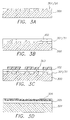
In FIG. 2 is shown a configuration for the transfer of a material which
has been deposited as a coating on the second substrate 200, onto the first substrate
201 as indicated by the arrows 205 and which is promoted by heating with heat source
202 as indicated by radiant heat 203 acting through an aperture 204.
Color filter arrays may be fabricated using evaporated colorants which
do not involve any receiving polymer. In order to fabricate such color filter arrays, a
typical process is as follows: A photoresist layer is coated on a transparent substrate
such as glass which is to be incorporated as an optical element in a device, for
example in a liquid crystal display, a light emitting diode display, an imaging sensor,
or other such device. Thereafter, the substrate is patterned to form openings over the
regions which are to pass filtered light or light which is to be filtered, depending on
the relative orientation of the substrate and the light source. Colorant materials,
generally pigments, are then deposited over the patterned photoresist layer to form a
colorant layer in the openings over the substrate. The unwanted colorant is removed
by chemical mechanical polishing, in which particles of an abrasive substance such as
silica with mean diameters of less than 0.5 micrometers are suspended in a fluid
medium such as aqueous tetramethylammonium hydroxide and the surface to be
polished is moved in relation to a pad which is wetted with the suspension. The
colorant which is positioned over the selected regions is not removed due to its lower
profile relative to the surface of the unwanted colorant. Alternatively, the unwanted
colorant may be removed by lifting-off the patterned photoresist layer and the
overlying colorant layer.
Color filter arrays may also be fabricated in another process, using
evaporated colorants which do not involve any receiving polymer. In order to
fabricate such color filter arrays on a substrate, such as an image sensor or on a
transparent substrate , a typical process is as follows: A colorant or a plurality of
colorants, generally pigments, is deposited on a substrate. Thereafter, a photoresist
layer is coated on the colorant layer and then patterned to leave photoresist in place
over selected regions of the substrate through which is to pass filtered light or light
which is to be filtered. An etch process is now performed and the patterned
photoresist layer acts as a mask for the colorant layer, such that the colorant is
removed except over the selected regions.
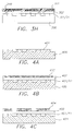
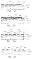
Turning next to FIG. 3A where substrate 300 is shown, the substrate,
which may be a transparent substrate such as glass, is shown with regions 31 through
which pass filtered light or light which is to be filtered, depending upon the
orientation of the substrate relative to the light source. The regions 31 in a transparent
substrate may actually extend to include the full thickness of the substrate, and are not
limited to only a portion of that thickness. For a silicon based substrate which are to
receive light, regions 31 can be processed beforehand to provide wells for different
dopant materials to form pixels 301. As is well understood to those skilled in the art,
the substrate may be a composite of different layers and in particular may include an
adhesion promoting layer 302.
As shown in FIG. 3B, an adhesion-promoting layer 302 is formed as
part of the substrate 300 and above regions 31 (or in pixels 301 in a silicon based
substrate). The adhesion-promoting layer 302 can be formed by a number of
techniques including spin-coating of an organic polymer or a spin-on glass, or by
chemical vapor deposition. The adhesion promoting layer may be patterned to form
recesses in the adhesion promoting layer above the pixels. Alternatively, the
adhesion-promoting layer 302 may be applied after formation of the patterned
photoresist layer 303, discussed below in FIG. 3C.
As shown in FIG. 3C, a spin-coated photoresist layer is patterned to
provide openings over the selected regions 31 (which can be pixels 301). Such
patterning techniques are well known to those skilled in the art. Typically, the
photoresist layer can be imagewise exposed to light, illuminating particular areas of
the layer. A development step is then used to form openings over the region 31
(pixels 301) providing the desired pattern.
As shown in FIG. 3D, where a second substrate 304 is provided (this
substrate typically is stainless steel, but other substrate materials can be used which
are heat resistant) a layer 305 having a colorant is formed on the substrate 304, and
another colorant layer 306 is formed on layer 305. Typically, the colorant layers are
formed by physical vapor deposition, which provides uniform layers of controlled
thickness, containing no materials with higher volatility than the colorants. The
colorant layers 305 and 306 can be organic colorants which are transferable upon the
application of energy such as heat. In a preferred embodiment of the present
invention, the colorant is vaporized by heating under reduced pressure, and condensed
on a moving strip of stainless steel foil which is passed over the heated source at a
constant rate.
It will be appreciated that instead of using multiple colorant layers 305
and 306, a single colorant layer may be employed as discussed in the second
embodiment, however the present discussion immediately below refers to the first
embodiment.
In FIG. 3E, the substrate 304 and colorant layers 305 and 306 are
shown positioned relative to the substrate 300 and the regions 31 (or pixels 301) in the
substrate. In the process it is desired to transfer the colorant layers 305 and 306 onto
the substrate and the pixels.
As shown in FIG. 3F, the transferred colorant layers are depicted as a
single layer now labeled number 307. In order to provide this transfer, heat is applied
to the substrate 304. Typically, the substrate is composed of metals, such as steel or
aluminum or of a temperature-resistant plastic such as a polyimide film. Heating is
often done by exposing the non-coated side of the substrate 304 to electromagnetic
radiation of wavelengths which are absorbed by the substrate (or by the colorant
coating in the cases where the substrate is substantially transparent) and are converted
into heat by radiationless decay processes. The electromagnetic radiation may be
applied over a large area simultaneously as from an extended lamp source, or it may
be applied as a scanned beam as with a laser. It is appreciated that imagewise light
exposure may be used to heat and transfer only a portion of the colorant coating.
Another method used to heat substrate 304 in order to transfer the colorant layers 305
and 306 is to pass an electric current through the substrate, particularly when the
substrate used is composed entirely or partially of metal. In still another method, the
substrate may be heated by direct contact with an object such as a metal block, a high
temperature roller, or other such devices which can be heated or pre-heated to the
required temperature and which can transfer heat to the substrate by direct thermal
contact. Typical distances and pressures for the transfer of colorant are from about 0.1
mm to about 3 mm at pressures of less than or equal to about 0.1 Torr, up to a distance
of about 50 mm at pressures of less than or equal to 0.001 Torr.
FIG. 3G shows the color filter array after a lift-off process. The lift-off
process is needed to remove unwanted portions of the photoresist layer 303 and the
portions of the colorant layer 307 on the unwanted portions of the photoresist layer
303, leaving behind colorant layers 38 over the selected regions 39 (or pixels 309).
More particularly, the lift-off process is as follows:
A photoresist layer is patterned by imagewise exposure to
electromagnetic radiation of the appropriate wavelength followed by development to
open up areas where a subsequently deposited layer is desired. The subsequent layer
is deposited on both the opened areas and the remaining photoresist, followed by the
lift-off, in which the photoresist is dissolved or swollen in a solvent, causing it to
become detached from the underlying substrate, lifting-off to leave the desired deposit
in place. A description of the lift-off process and typical materials used is given in
chapter 12 of Semiconductor Lithography, by W.M. Moreau, Plenum Press, N.Y.,
1989.
In order to make a color filter array with a plurality of colors, the above
steps need to be repeated for each new colorant layer that is deposited over pixels.
A second embodiment for the preset invention is seen viewing FIG. 3H
with respect to FIG. 3F. In this embodiment the color filter is seen after a chemical
mechanical polishing process. The chemical mechanical polishing process is needed
to remove unwanted portions of the photoresist layer 303 and portions of layer 307
(which can be one or more colorant layers) leaving behind colorant layers 310 of the
selected regions 31 (or pixels 301) and photoresist layer 311 over the remaining areas.
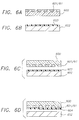
Turning to FIG. 4A, where substrate 40 is shown, the substrate (which
can be either a silicon substrate or a transparent substrate such as glass) in which are
depicted regions 41 through which filtered light will pass or light that is to be filtered
(regions 41 can be pixels 401 which are to receive filtered light, in the case of a
silicon substrate which has already been processed to provide wells for different
dopant materials (to form pixels 401). As is well understood to those skilled in the
art, the substrate may be a composite of different layers, and in particular may include
an adhesion promoting layer.
As shown in FIG. 4B, an adhesion promoting layer 402 which can be
subsequently etched is formed as part of the substrate 400 with regions 41 (which can
be pixels 401) and a layer of photoresist 403 is formed above it.
As shown in FIG. 4C, the photoresist is exposed and developed to form
openings over selected regions 41 (or pixels 401), leaving photoresist 404 over the
rest of the layer 402.
As shown in FIG. 4D, the openings in the patterned resist layer 404 are
used as a mask for an etch of the substrate 400, to produce a pattern of recesses in the
adhesion promoting layer, now numbered 405. Alternatively, the etch may be
performed so as to etch through the adhesion promoting layer 405 into the rest of
substrate 400.
As shown in FIG. 4E, a colorant layer is deposited on the patterned
resist layer 404 and the recesses in underlying layer 405 to give layer 406/407.
As shown in FIG. 4F, the colorant 406 which is not above the selected
regions 41 (which can be pixels 401 in the case of a silicon substrate) and the
patterned photoresist layer 404 is removed by chemical mechanical polishing, to leave
the patterned layer 405 and the colorant 407 above the selected regions 41 (or pixels,
401).
In order to make a color filter array with a plurality of colors, the above
steps need to be repeated for each new colorant layer that is deposited over
subsequently selected pixels.
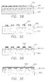
Turning now to FIG. 5A, in which a substrate 500 (which can range
from a transparent glass to a silicon based substrate) is shown having regions 51
through which filtered light will pass or light which is to be filtered. In the case where
the substrate 500 is silicon, the substrate can already have been processed to provide
wells for different dopant materials to form pixels 501 which are to receive filtered
light. As is well understood to those skilled in the art, the substrate may be a
composite of different layers, and in particular may include an adhesion promoting
layer.
As shown in FIG. 5B, an adhesion promoting layer 52 which can be
etched is formed on the substrate 50 and the regions 51 (which in the case of a silicon
substrate can be pixels 501), and a photoresist layer 53 is formed above it.
As shown in FIG. 5C, the photoresist is exposed and developed to form
the patterned photoresist layer 504, having openings above the selected regions 51
(which could be pixels 501).
As shown in FIG. 5D, a recessed pattern is formed in the adhesion
promoting layer 505 by etching through the patterned photoresist layer 504 as a mask.
Alternatively, the etch may be performed so as to etch through adhesion promoting
layer into the rest of the substrate.
As shown in Fig, 5E, another layer of photoresist is formed on the
patterned layer 505, and the two photoresist layers are shown as a single layer 506.
As shown in FIG. 5F, the second photoresist layer is exposed and
developed to form a patterned resist layer 507, with openings above second selected
regions 515.
As shown in FIG. 5G, a colorant layer is deposited on the patterned
resist layer 507 and above the second selected regions 515 (which is a subset of first
selected regions 51 which can be pixels 501 in a silicon embodiment)to give layers
508/509.
As shown in FIG. 5H, the colorant layer 508, which is not above the
second selected regions 515, and the patterned photoresist layer 507 are removed to
leave colorant 509 above the second selected regions 515 leaving the second
photoresist 510 above the other regions. Methods for removing the colorant layer and
photoresist layer include chemical mechanical polishing, to leave colorant 509 above
the second selected regions 515, and photoresist 510 above the other pixels.
As shown in FIG. 5I, the photoresist over the regions not selected is
exposed and developed to remove it from above those areas, leaving openings 511 in
the etched layer 505.
In order to make a color filter array with a plurality of colors, the steps
5E-5I need to be repeated for each new color.
Colorants which are useful in the processes shown in FIGS. 3A-G, 4A-F,
and 5A-I include the following: phthalocyanines, such as Pigment Blue 15, nickel
phthalocyanine, chloroaluminum phthalocyanine, hydroxyaluminum phthalocyanine,
vanadyl phthalocyanine, titanyl phthalocyanine, and titanyl tetrafluorophthalocyanine;
isoindolinones, such as Pigment Yellow 110 and Pigment Yellow 173; isoindolines,
such as Pigment Yellow 139 and Pigment Yellow 185; benzimidazolones, such as
Pigment Yellow 151, Pigment Yellow 154, Pigment Yellow 175, Pigment Yellow
194, Pigment Orange 36, Pigment Orange 62, Pigment Red 175, and Pigment Red
208; quinophthalones, such as Pigment Yellow 138; quinacridones, such as Pigment
Red 122, Pigment Red 202, and Pigment Violet 19; perylenes, such as Pigment Red
123, Pigment Red 149, Pigment Red 179, Pigment Red 224, and Pigment Violet 29;
dioxazines, such as Pigment Violet 23; thioindigos, such as Pigment Red 88, and
Pigment Violet 38; epindolidiones, such as 2,8-difluoroepindolidione; anthanthrones,
such as Pigment Red 168; isoviolanthrones, such as isoviolanthrone; indanthrones,
such as Pigment Blue 60; imidazobenzimidazolones, such as Pigment Yellow 192;
pyrazoloquinazolones, such as Pigment Orange 67; iketopyrrolopyrroles, such as
Pigment Red 254, Irgazin DPP Rubin TR, Cromophtal DPP Orange TR;
Chromophtal DPP Flame Red FP (all of Ciba-Geigy); and bisaminoanthrones, such as
Pigment Red 177.
The foregoing description as illustrated the two embodiments of the
present invention for making color filters via close space sublimation. The first
embodiment employs a lift off procedure and the second employs chemical
mechanical polishing. Below is a third embodiment the details close space
sublimation by colorant transfer and etch.
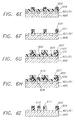
Turning next to FIG. 6A where a substrate 600 is shown. The substrate
if silicon has already been processed to provide wells for different dopant materials to
form regions 601, which are pixels in the cases for a silicon substrate. If a transparent
substrate is used these regions 61 will pass filtered light or light which is to be
filtered, depending on the orientation of the substrate relative to the light source. As is
well understood to those skilled in the art, the substrate may be a composite of
different layers and in particular may include an adhesion promoting layer. For a
more complete description of the construction of image sensors, see commonly
assigned U.S. Patent No. 5,235,198.
As shown in FIG. 6B, where a second substrate 602 is provided. This
substrate typically is stainless steel, but other substrate materials can be used which
are heat resistant. A first colorant layer 603 is formed on the substrate 602.
As shown in FIG. 6C, the substrate 602 and first colorant layer 603 is
shown positioned relative to the substrate 600 and the regions 61 in the substrate. In
the process it is desired to transfer the colorant layer 603 onto the substrate 600.
As shown in Fig 6D, the transferred colorant layer is now labeled
number 604. In order to provide this transfer, heat is applied to the substrate 602.
As shown in FIG. 6E, a photoresist layer 605 is formed and patterned
on the first colorant layer 604 to provide protection of portions of the colorant layer
over first selected regions 61. Such patterning techniques are well known to those
skilled in the art. Typically, the photoresist layer 605 can be imagewise exposed to
light, illuminating particular areas of the layer 605. A development step is then used
to form openings in all areas except over the first selected regions 61 providing the
desired pattern.
As shown in FIG. 6F, the portions of the first colorant layer 604 not
covered by the photoresist 605 are removed by etching, in which the photoresist 605
acts as a mask, such that colorant is left behind only over the first selected regions 61
As shown in FIG. 6G, a second colorant layer 607 is deposited on the
first substrate 600, over the first selected regions 61, and over the remaining regions
608 and 609. The same process is used to deposit the second colorant layer as was
used to deposit the first colorant layer.
As shown in FIG. 6H, a photoresist layer 610 is formed and patterned
over the second colorant layer, above second selected regions 608.
As shown in FIG. 6I, an etch step removes the second colorant layer
except above the second selected regions, where it is protected by photoresist layer
608, leaving a patterned second colorant layer 611.
The steps g)-i) are repeated for each additional colorant layer desired.
Colorants which are useful in the process for the third embodiment are
the same as in previously discussed. The Examples are also the same as previously
described.
EXAMPLES
In accordance with the above-stated invention, the following has been
performed.
Example 1: A tantalum boat was half-filled with about 0.1 gm of
Pigment Yellow 110 (Ciba-Geigy Corp.), placed under a partial vacuum of about
2.5X10E-5 Torr, and heated to a temperature of 375-417 degrees C by passing an
electric current through it. The material which evaporated from the boat was
condensed on a section of stainless steel foil, about 25 microns thick, maintained at
ambient temperature. The thickness of the deposit was monitored by an oscillating
quartz crystal monitor, and was stopped when the thickness reached about 0.45
microns.
In a similar fashion, the coated steel foil was coated with about 0.15
microns of titanyl phthalocyanine (H.W. Sands Co.), at a pressure of about 2X10E-4
Torr and over a temperature range of 331-437 degrees C.
The double-coated steel foil was positioned about 2 mm from a glass
slide, clamped between two electrodes, placed in a partial vacuum of about 3.3X10E-5
Torr, and heated by the passage of an electric current at 30 volts for 10 sec. All of the
colorants were found to have transferred to the glass slide, giving a clear, continuous
layer with an optical density above 3.0 at 695-715 nm. Attempts to mechanically
separate the transferred colorants into distinct layers were unsuccessful.
Example 2: A similar procedure was followed as given in Example 1,
except that the colorants were deposited in the reverse order. The colorants
transferred completely to the glass slide, and appeared to form a clear, continuous
layer.
Example 3. Commercially obtained titanyl phthalocyanine (Aldrich
Chemical Co.) was placed in a tantalum boat and heated by passing electrical current
through it, while maintaining a reduced pressure of about 1.1X10E-4 Torr in a
vacuum bell jar. About 0.15 microns of the phthalocyanine were deposited onto a
section of stainless steel foil, having a thickness of about 25 microns. The coated foil
was used as the substrate for a second colorant layer in a second step, heating
Pigment Orange 36 (Novoperm Orange HL-70 from Hoechst Celanese Corp.) in a
tantalum boat at a pressure of about 1.3 X 10E-4 Torr. About 0.3 microns of the
pigment were deposited on the phthalocyanine coating, forming a double-layer coating
on the steel foil. The double-coated foil was then mounted about 2 mm distant from a
section of a silicon wafer bearing an adhesion promoting layer of 1.0 microns of
poly(methyl glutarimide) (PMGI from Microelectronics Chemical Corp.) and a
patterned layer of AZ5214IR photoresist (Hoechst Celanese Corp.), and the foil was
clamped between two electrodes. The assembly was subjected to a vacuum of about
1.1 X 10E-4 Torr, and electric current was passed through the foil (at 30 volts) for
about 10 sec. Both the phthalocyanine and the Pigment Orange 36 transferred to the
wafer. The wafer was subjected to 30 sec. in acetone in an ultrasonic bath (Branson
2200) which removed the photoresist and the pigment which was on top of it, leaving
pigment features in the desired locations on the wafer.
Example 4. Commercially obtained copper phthalocyanine was heated
by passing electrical current through the tantalum boat which contained it, while
maintaining a reduced pressure of approximately 6 x 10⁻⁵ Torr in a vacuum bell jar.
About 0.2 microns of phthalocyanine were deposited onto a section of stainless steel
foil, having a thickness of about 25 microns. The coated foil was then mounted about
3 mm distant from a silicon wafer which had been spin-coated with about 1 micron of
poly(methyl glutarimide), "PMGI" from Microelectronics Chemical Corp., and then
coated with about 1.3 microns of photoresist AZ5214IR (Hoechst Celanese Corp.)
which was subsequently patterned and developed, and the non-coated side of the foil
was positioned about 25 mm from an array of heat lamps (General Electric, Part no.
QH500T3/CL) spaced about 30 mm apart. The assembly was subjected to a vacuum
of about 6 x 10E-5 Torr and the heat lamps were powered for 60 seconds to transfer
the phthalocyanine to the silicon wafer. The water was removed from the vacuum
chamber and subjected to ultrasound in a tray of acetone for 90 seconds, using a
Branson Model 3200 ultrasonic bath. The photoresist was completely removed by
this treatment, leaving intact the copper phthalocyanine features in the desired pattern.
Example 5. Commercially obtained copper phthalocyanine was heated
by passing electrical current through the tantalum boat which contained it, while
maintaining a reduced pressure of about 6X10E-5 Torr in a vacuum bell jar. About
0.2 microns of phthalocyanine were deposited onto a section of stainless steel foil,
having a thickness of about 25 microns. The coated foil was then mounted about 3
mm distant from a glass substrate, and the foil was clamped between two electrodes.
The assembly was subjected to a vacuum of about 0.1 Torr, and electric current was
passed through the foil (at 30 volts) for about 10 sec., causing the ends of the foil to
reach a temperature of about 260 degrees C and the phthalocyanine to transfer to the
glass substrate.
The foregoing description as illustrates the embodiments most
preferred for making color filters via close space sublimation. Variations of these
embodiments will be readily apparent to those skilled in the art, accordingly the scope
of the present invention should be measured in view of the appended claims.
Parts List
- 31
- regions
- 39
- regions
- 41
- regions
- 51
- regions
- 61
- regions
- 100
- heat source
- 102
- substrate
- 103
- paths
- 104
- mask
- 105
- mask
- 200
- second substrate
- 201
- first substrate
- 202
- heat sources
- 203
- radiant heat
- 204
- aperture
- 205
- direction arrows
- 300
- substrate
- 301
- pixels
- 302
- adhesion promoting layer
- 303
- photoresist layer
- 304
- substrate
- 305
- colorant layer
- 306
- colorant layers
- 307
- colorant layer
- 308
- colorant
- 309
- pixels
- 310
- colorant
- 311
- photoresist
- 400
- substrate
- 401
- pixels
- 402
- layer
- 403
- photoresist
- 404
- photoresist
- 405
- adhesion promoting layer
- 406
- colorant layer
- 407
- colorant layer
- 500
- substrate
- 501
- pixels
- 502
- adhesion promoting layer
- 503
- photoresist layer
- 504
- photoresist layer
- 505
- adhesion promoting layer
- 506
- photoresist layer
- 507
- photoresist layer
- 508
- colorant layer
- 509
- colorant layer
- 510
- photoresist
- 511
- openings
- 600
- substrate
- 601
- pixels
- 602
- second substrate
- 603
- colorant layer
- 604
- colorant layer
- 605
- photoresist layer
- 607
- colorant layer
- 608
- regions
- 609
- regions
- 610
- photoresist layer
- 611
- colorant layer