EP0858164A2 - Semiconductor device protection circuit - Google Patents
Semiconductor device protection circuit Download PDFInfo
- Publication number
- EP0858164A2 EP0858164A2 EP98107173A EP98107173A EP0858164A2 EP 0858164 A2 EP0858164 A2 EP 0858164A2 EP 98107173 A EP98107173 A EP 98107173A EP 98107173 A EP98107173 A EP 98107173A EP 0858164 A2 EP0858164 A2 EP 0858164A2
- Authority
- EP
- European Patent Office
- Prior art keywords
- fet
- temperature
- terminal
- semiconductor device
- protection circuit
- Prior art date
- Legal status (The legal status is an assumption and is not a legal conclusion. Google has not performed a legal analysis and makes no representation as to the accuracy of the status listed.)
- Withdrawn
Links
Images


Classifications
-
- H—ELECTRICITY
- H03—ELECTRONIC CIRCUITRY
- H03K—PULSE TECHNIQUE
- H03K17/00—Electronic switching or gating, i.e. not by contact-making and –breaking
- H03K17/16—Modifications for eliminating interference voltages or currents
- H03K17/161—Modifications for eliminating interference voltages or currents in field-effect transistor switches
- H03K17/165—Modifications for eliminating interference voltages or currents in field-effect transistor switches by feedback from the output circuit to the control circuit
-
- H—ELECTRICITY
- H03—ELECTRONIC CIRCUITRY
- H03K—PULSE TECHNIQUE
- H03K17/00—Electronic switching or gating, i.e. not by contact-making and –breaking
- H03K17/08—Modifications for protecting switching circuit against overcurrent or overvoltage
- H03K17/082—Modifications for protecting switching circuit against overcurrent or overvoltage by feedback from the output to the control circuit
- H03K17/0822—Modifications for protecting switching circuit against overcurrent or overvoltage by feedback from the output to the control circuit in field-effect transistor switches
-
- H—ELECTRICITY
- H03—ELECTRONIC CIRCUITRY
- H03K—PULSE TECHNIQUE
- H03K17/00—Electronic switching or gating, i.e. not by contact-making and –breaking
- H03K17/08—Modifications for protecting switching circuit against overcurrent or overvoltage
- H03K2017/0806—Modifications for protecting switching circuit against overcurrent or overvoltage against excessive temperature
Definitions
- the present invention relates to the general field of semiconductor device protection circuits wherein such circuits protect a semiconductor device by minimizing either applied voltage, through current and/or power dissipation so as to enable the device to survive. More particularly, the present invention is directed to protecting semiconductor devices, such as field effect transistors (FETs), so that they can survive excessive voltages, currents and/or power dissipation which may be produced during load dump conditions.
- FETs field effect transistors
- protection circuits which turn the FET off if conditions such as overcurrent, excessive FET power dissipation or excessive FET temperature are detected.
- U.S. patent 4,896,245 to Qualich and U.S. patent 4,937,697 to Edwards et al. are examples of such prior protection circuits.
- Such protection circuits typically do not provide sufficient protection for the FET during load dump conditions during which substantial excessive voltages can be applied between the drain and source terminals potentially causing undesired avalanche breakdown of some internal junctions of the FET semiconductor device. This can occur regardless of the operation of the above noted turn-off circuits.
- Some FET protection circuits have utilized a zener diode connected between the drain and gate electrodes to protect the FET by turning the device on in response to a load dump voltage in excess of the zener diode breakdown voltage.
- Such circuits may not provide sufficient protection since they can result in excessive FET power dissipation during repetitive switching of the FET on and off during the load dump transient.
- Pending U.S. patent application SN 07/484,313, filed February 26, 1990 to Edwards European patent application 91102174.9 filed February 15, 1991 proposes one solution to this problem by utilizing a capacitor as a supplementary supply of operative power to maintain the FET on during a load dump condition.
- sensed temperature is used to determine a temperature threshold above which a control circuit will control an output stage, but typically such circuits and any adjustment of the temperature threshold are not implemented in a cost effective manner.
- An object of the present invention is to provide an improved semiconductor device protection circuit which overcomes some of the above noted problems of the previous protection circuits.
- the invention provides a semiconductor device protection circuit comprising:
- the present invention provides an improved semiconductor device protection circuit in which in one embodiment semiconductor device temperature above a temperature threshold is used to modify a control signal applied to the semiconductor device and wherein a majority of the the protection circuit is provided on an integrated circuit, while an external component is provided which allows external adjustment of the temperature above which the semiconductor device control signal will be modified.
- the improved semiconductor device protection circuit enables the semiconductor device to withstand load dump transient signals.
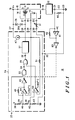
- a semiconductor device protection circuit 10 which includes a semiconductor device 11, that forms a driver stage for controlling the current supplied to a low resistance, high current rated load 12 .
- the device 11 preferably comprises a FET and the load 12 preferably comprises the windings of a motor.
- the FET 11, along with a polysilicon temperature sensing diode 13 are provided inside an integrated circuit module 14 (shown dashed in Figure 1).
- the diode 13 is positioned adjacent the FET 11 such that the diode 13 will sense the temperature of the FET and produce a voltage thereacross substantially corresponding to the temperature of the FET due to close thermal coupling between the diode and the FET.
- a drain electrode D of the FET 11 is connected to an external terminal 15 of the module 14 that is directly connected to a power supply terminal 16 at which a positive battery supplied power supply voltage V+ is provided.
- a gate electrode G of the FET is connected to an external input terminal 17 of the module 14 and a source electrode S of the FET is connected to an external terminal 18 of the module 14.
- Anode and cathode electrodes of the temperature sensing diode 13 are connected to external terminals 19 and 20 of the module 14, respectively.
- the terminal 18 is directly connected as a current input to the motor winding load 12 which has a terminal 21 connected through a direct wire connection 22 to a terminal 23 at which ground potential is provided.
- the FET 11 comprises a semiconductor device which receives at least one device control signal at its gate control electrode, corresponding to the terminal 17 and, in response thereto, selectively passes current through the FET 11 between a pair of output electrodes of the FET corresponding to the drain and source electrodes which correspond to the terminals 15 and 18, respectively. This current is provided to the motor load 12.
- the temperature sensing diode 13 comprises a temperature sense means which is thermally coupled to the FET 11 for developing a temperature sense signal across the diode 13 which has a magnitude indicative of the temperature of the FET.
- the protection circuit 10 includes a control circuit 24 (shown dashed) which represents a plurality of electrical components provided on an integrated circuit (IC).
- the control circuit 24 is coupled to the temperature sensing diode 13 for receiving the temperature sense signal developed thereacross and selectively determining the device control signal provided at the terminal 17 in accordance with the temperature sense signal and in accordance with an external control signal received at an input terminal 25.
- the control circuit 24 responds to the external control signal at the terminal 25 to selectively control the on/off conduction of the FET 11 so as to provide current to the motor winding load 12 in accordance with the signal at the terminal 25.
- the control circuit 24 will modify the device control signal provided at the terminal 17 so as to protect the FET 11 and prevent destruction of this device due to certain conditions, including load dump.
- load dump refers to a transient condition wherein an exceptionally higher than normal voltage is provided at the terminal 16 wherein such voltage is large enough to cause excessive power dissipation in the FET 11 due to undesired avalanche breakdown of semiconductor junctions in the FET. This undesired breakdown can result in excessive power dissipation and permanent destruction of the FET.
- the present invention contemplates selectively turning the FET on during a load dump condition to allow the FET to survive the load dump transient condition. This is implemented in accordance with sensed FET temperature in such a manner that the FET is reliably protected during load dump.
- a zener diode 26 and a diode 26A are connected between the terminals 15 and 17 with the cathode of the zener diode connected to the terminal 15.
- the anodes of the diodes 26 and 26A are connected together and the cathode of diode 26A is connected to terminal 17.
- the zener diode 26 ensures that if the FET 11 was receiving an off control signal at the terminal 17 prior to load dump, during load dump the high voltage at the terminal 15 would breakdown the zener diode 26, forward bias diode 26A and provide a sufficient gate voltage to turn the FET on during load dump.
- an unloaded load dump voltage of over 80 volts can occur when the voltage V+ corresponds to the alternator output terminal of a vehicle battery charging system in an automobile.
- the zener diode 26 having a typical value of 28 volts, this will result in a drain-to-source voltage of 30 volts during load dump.
- the motor load 12 typically has a very low impedance of the order of less than one ohm, a substantial current can flow through the FET during load dump resulting in damage to the FET for a long load dump transient. This can occur even if the zener diode 26 turns the FET on and keeps it on during load dump.
- the voltage at the terminal 15 may now drop abruptly and this may result in stopping the breakdown of zener diode 26.
- the end result can be periodic switching of the FET on and off during load dump. During these switching transients large average drain-to-source voltages and large average currents can exist which result in excessive power dissipation of the FET that can readily result in damage to the FET.
- the present invention prevents this type of excessive power dissipation of the FET during load dump. This is accomplished in the following manner.
- Control circuit 24 Power to the control circuit 24, which corresponds to an IC, is received at an external input terminal 27 which is directly connected to the power supply terminal 16.
- a control output provided by the control circuit 24 is provided at an external terminal 28 which is directly connected to the terminal 17.
- the terminals 19 and 20 of the temperature sensing diode 13 are connected to external terminals 29 and 30 of the control circuit 24.
- An adjustable or selectable resistor 31 is provided external to the control circuit 24 and between the terminals 20 and 30 and a direct electrical connection is provided between the terminals 19 and 29.
- Ground potential is provided to the control circuit 24 by an external terminal 32 which is directly connected to the ground terminal 23.
- the external input terminal 25 is connected as an input to an AND gate 33 that provides an output at a terminal 34 which serves as an input to an OR gate 35.
- the OR gate 35 provides an output at a terminal 36 that is connected as an input to a charge pump circuit 37 whose output is directly connected to and provided at the terminal 28.
- charge pump 37 will provide a high voltage at terminal 28 to fully turn on the FET 11.
- Diode 26A prevents this high voltage at terminal 28 from being shorted to the V+ voltage at terminal 16.
- Semiconductor device overtemperature turn-off circuitry is provided within the control circuit 24 and comprises the following components.
- a stable reference voltage V REF is provided at a terminal 38 .
- the terminal 38 is coupled through an integrated circuit resistor 39 to a terminal 40 at which a reference potential V 1 is provided.
- a resistor 41 is provided between the terminal 40 and a terminal 42 at which a reference voltage V2 is provided and a resistor 43 is connected between the terminal 42 and ground potential.
- the components 38-43 form a resistor divider which provides reference voltages V 1 and V 2 with a predetermined difference relationship therebetween.
- the terminal 40 is directly connected to the positive input of a comparator 44 whose output is coupled through an inverter 45 as an input to the AND gate 33.
- a resistor 46 is provided between the positive input of the comparator 44 and its output to provided a degree of hystersis with regard to the switching threshold of this comparator.
- a negative input terminal of the comparator 44 is directly connected to the terminal 29 and a constant current source 47 is connected between the terminals 27 and 29 and provided within the integrated circuit 24.
- the terminal 30 is directly connected to the terminal 32.
- a high or positive logic signal is provided at the input terminal 25, this indicates that it is desired to turn on the FET 11.
- This signal is received by the AND gate 33 and will be passed through to the charge pump 37 if the temperature of the FET is below 150°C.
- the constant current source 47 provides a known predetermined current through the temperature sensing diode 13 and the adjustable/selectable resistor 31 to ground. With this configuration, the voltage at the terminal 19 varies in accordance with the temperature of the FET 11, and this voltage can be adjusted by the selection of the magnitude of the resistor 31. This occurs because it is known that the voltage across a polysilicon diode, such as the diode 13, varies in a known predetermined manner in accordance with the temperature of such a diode, and the diode temperature will correspond to the FET temperature.
- the diode 13 provides a temperature sense voltage at the terminal 19 related to the temperature of the FET 11.
- the resistor 31 permits external, with respect to the control circuit 24, adjustment of the absolute magnitude of this voltage. It should be noted that the voltage across the temperature sensing diode 13 will, as is known, vary inversely with respect to the temperature of the diode such that the voltage across the diode 13 will have a negative TC. The magnitude of the resistor 31 is selectively adjusted such that at a FET temperature of 150°C, the voltage at the terminal 29 will equal the voltage V1.
- the comparator 44 will provide a positive output which, via the inverter 45, prevents the AND gate 33 from passing the external control signal at the terminal 25 to the OR gate 35.
- the comparator 44 will prevent the signal at the terminal 25 from providing a positive logic input to the charge pump 37 and therefore prevent this signal from turning on the FET.
- This configuration generally corresponds to the prior overtemperature turn-off circuitry used in previous circuits, except that the providing of the resistor 31 external to the control circuit IC allows an external adjustment of the switching threshold to provide greater accuracy for the turn-off protection feature of the present invention.
- the resistor 46 is used to provide some hystersis such that rapid oscillating switching of the comparator 44 between its high and low output states will not occur for very minor changes in temperature of the FET 11 and temperature sensing diode 13.
- a major feature of the present invention is to effectively turn-on the FET 11, at least during load dump, if excessive power dissipation, as indicated by temperature, of the FET 11 is sensed despite the operation of the overtemperature shut-off circuitry. This occurs in the following manner.
- the control circuit 24 includes a maximum temperature comparator 50 having a positive input thereof directly connected to the terminal 42 and a negative input thereof connected through a resistor 51 to the terminal 29.
- the output of the comparator 50 is provided as an additional input to the OR gate 35.
- This configuration ensures that the charge pump 37 will receive an on control signal input if the temperature of the FET 11 exceeds a maximum threshold temperature of 160°C despite the operation of the 150°C temperature shut-off circuitry that includes the comparator 44 and AND gate 33. This is believed to be contrary to all prior circuits wherein this maximum temperature threshold of 160°C is above the turn off temperature of 150°C and is close to the maximum rated junction temperature of 175°C for the FET 11.
- the term "close to the maximum rated junction temperature”, is used to indicate a device temperature of at least more than 30°C below the maximum rated junction temperature of the FET 11. The significance of this is that if the power dissipation, and therefore the temperature, of the FET 11 is exceeded despite the operation of the overtemperature shut-off circuitry comprising the comparator 44 and AND gate 33, then the comparator 50 will cause the charge pump 37 to turn-on the FET so as to increase conduction therethrough and thereby attempt to minimize power dissipation of the FET 11. This will occur anytime the temperature of the FET 11 exceeds the maximum temperature threshold of 160°C. This is best understood by referring to the circuitry in Figure 1 in conjunction with the graphs shown in Figures 2A-2E which demonstrate operation of the present invention during load dump.
- FIG. 2A a graph of the unloaded voltage V+ at the terminal 16 is illustrated.
- the magnitude of the voltage V+ is maintained at positive 12 volts since this voltage corresponds to the regulated battery voltage of an alternator charging system in a vehicle.
- load dump occurs. In an alternator charging system, this can occur due to the sudden removal of a resistive load from the alternator charging system. In such a case, there is an extremely rapid increase in the voltage V+ to some maximum value, such as 80 volts. This increase can exist for a substantial period of time. If protection circuitry were not provided this increase can result in junction breakdown of the FET and/or excessive power dissipation resulting in the permanent destruction of the FET 11.
- FIG. 2A illustrates the unloaded load dump voltage which would exist at terminal 16 if the FET 11 never conducted current and the zener diode 26 did not breakdown. However, when the voltage V+ increases to beyond the breakdown voltage of the zener diode 26, this diode will breakdown and provide a biasing voltage at the gate of the FET 11. Subsequently, the FET 11 will turn-on and typically a 2 volt on bias will exist between the gate and source electrodes of the FET 11 resulting in a 30 volt drain-to-source voltage across the FET 11. With the FET 11 turned on, current will then flow through the motor load 12 wherein the load 12 is assumed to be less susceptible to load dump overcurrent and overvoltages such that it can more readily survive excessive voltage and current transients. It is assumed that only a negligible voltage drop will exist across the motor load 12 due to its low resistance.
- the overtemperature shut-off circuitry comprising the comparator 44 and AND gate 33, would result in the charge pump 37 being effectively turned off at 150°C.
- the signal waveforms in Figures 2A-2E illustrate the case where the control signal at the terminal 25 does not try to maintain the FET on prior to or during load dump.
- the comparator 50 will now turn on the charge pump 37. This results in essentially turning on the FET 11 harder, since the FET was already turned on by the zener diode 26.
- Figures 2B-2E show operation of the circuit 10 for a load 12 which is primarily a large inductance
- Figures 2D and 2E are representative of circuit operation for a purely resistive load 12.
- currents through the load 12 and the FET 11 tend to remain the same despite any tendency of the FET 11 to start to turn off during load dump.
- changes in V DS and T FET are minimized and occur at a slower rate.
- FET power dissipation is less and there is no further increase in the FET temperature.
- the FET starts to cool below 160°C, the FET starts to come out of its fully enhanced mode due to the charge pump 37 starting to turn off. This again increases power dissipation and FET temperature such that a 160°C FET temperature is substantially maintained during load dump till a time t 4 .
- the V+ voltage at the terminal 16 has fallen to such a low voltage during load dump that starting to bring the FET 11 out of its fully enhanced conduction will no longer result in increasing FET temperature.
- the FET temperature will then go below the 160°C threshold of comparator 50 and the comparator will now no longer result in the charge pump 37 fully enhancing the FET.
- the FET 11 will then turn-off, assuming no turn-on input at the terminal 25, and the FET temperature will continue to cool off to ambient temperature.
- the protection circuit 10 has prevented excessive power dissipation in the FET by turning on the FET harder during a load dump condition and therefore minimizing the power dissipation of the FET. It should be noted that just keeping the FET off during the entire load dump condition would not protect the FET since then the excessive voltage at the terminal 16 would cause breakdown of the internal junction diodes of the FET resulting in destruction of this device.
- components 60 to 63 are illustrated as being connected in dashed form to other circuitry in Figure 1. If connected these components implement an overcurrent turn-off function in addition to the over temperature turn-off function implemented if FET temperature exceeds 150°C.
- the direct connection 22 is replaced by a current sensing resistor 60 and the terminal 21 is connected to the positive input of a comparator 61 that receives a maximum current reference voltage I max at its negative input terminal.
- a hystersis resistor 62 is connected between the positive input and output of the comparator 61, and the output is coupled through an inverter stage 63 as an additional input to the AND gate 33.
- the configuration of the circuit 10 could be altered such that the current turn-off function of comparator 61 would override the temperature turn-on function implemented by the comparator 50. This would just involve coupling the output of the comparator 50 to the OR gate 35 through an additional AND gate which would receive another input from the output of inverter 63. If the current maximum I max is actually such a large current that any current above this maximum would destroy circuit paths or wire bonds relating to the FET 11, then this latter configuration would be desired. However, typically the maximum current I max is just another measure of excessive power dissipation, similar to the 150°C power dissipation level, and therefore the output of the inverter 63 should be connected as an additional input to the AND gate 33.
- FIG. 1 While the circuit of Figure 1 comprises the preferred embodiment for the present invention, an alternative circuit 100 is illustrated in Figure 3 in which all of the elements 11 through 47 in Figure 1 are reproduced and are identical in function and configuration. However, in Figure 3 instead of the comparator 50 a different configuration for the overtemperature turn-on circuitry of the present invention is implemented.
- the overtemperature threshold voltage V 2 at the terminal 42 is provided as an input to the positive input of a comparator 150 which has its negative input connected through a resistor 151 to the terminal 29.
- the output of the comparator 150 is provided at a terminal 152 which is provided as an input to an AND gate 153 and coupled through an inverter 154 to a reset terminal R of a set/reset flip-flop 155.
- the output of the AND gate 153 is provided at a terminal 156 which is connected to a set terminal S of the flip-flop 155, and an output Q of the flip-flop is directly connected as an input to the OR gate 35.
- a 28 volt zener diode 157 is connected between the V+ terminal 27 and a terminal 158 connected as an input to the AND gate 153.
- a resistor 159 is connected between the terminal 158 and ground potential.
- the components 150 through 159 in Figure 3 implement an overtemperature turn-on function for the circuit 100. While the temperature is below 160°C, the comparator 150 will produce a low logic state at the terminal 152 resulting in maintaining the flip-flop 155 at its reset state during which the flip-flop output Q is maintained at a low logic state. During a condition of load dump, the zener diode 157, as is the case with the zener diode 26, will breakdown due to the large voltage at the terminal V+. This results in a high logic input at the terminal 158.
- the comparator 150 When during such a load dump condition, the temperature of the FET 11 exceeds 160°C (corresponding to the threshold voltage V 2 ), the comparator 150 will produce a high logic state at the terminal 152 resulting in the setting of the flip-flop output Q high. This results in activating the charge pump 37 so as to ensure that the FET 11 is turned on in a fully enhanced mode of conduction. The output of the flip-flop 155 will remain high, regardless of the continued breakdown of the zener diode 157, until the temperature of the FET 11 falls below the switching level of the comparator 150.
- Adjustment of the external resistor 31 adjusts the magnitude of the temperature variable signal at the terminal 29. This not only allows the adjustment of the maximum turn-off FET temperature corresponding to the 150°C threshold for the FET 11, but also allows the simultaneous adjustment of the maximum turn-on temperature threshold utilized by the comparators 50 and 150. If desired, each of these thresholds could be separately adjusted by suitable modification of the control circuit 24 and/or providing an additional output terminal and additional adjustable resistors external to the control circuit 24.
Abstract
Description
Claims (8)
- A semiconductor device protection circuit comprising:semiconductor device (11) for receiving at least one device control signal (at 28) at a control electrode (G) and, in response thereto, selectively passing current through the device between a pair of output electrodes (D, S) of the device;temperature sense means (13) coupled to said device (11) for developing a temperature sense signal (at 29, 30) having a magnitude indicative of the temperature of said device; andcontrol means (24, 31) coupled to said temperature sense means for receiving said temperature sense signal and selectively modifying said device control signal in response to said sensed device temperature exceeding a temperature threshold;wherein the protection circuit is characterized by a majority of said control means (24, 31) being provided on a control integrated circuit (24) and means (31), external to said integrated circuit (24), for allowing external adjustment of the device temperature at which said control means will modify said device control signal.
- A semiconductor device protection circuit according to claim 1 wherein said temperature sense means (13) includes a temperature sensing diode positioned adjacent said semiconductor device (11) and wherein said external adjustment means (31) comprises at least one resistor (31) external to said integrated circuit.
- A semiconductor device protection circuit according to claim 2 wherein said external resistor (31) is connected in series with said temperature sensing diode (13) and said external resistor has a magnitude which determines said temperature sense signal magnitude.
- A semiconductor device protection circuit according to claim 2 wherein said external resistor (31) is adjustable.
- A semiconductor device protection circuit according to claim 1 wherein said control means (24, 31) increases on conduction of said device (11) in response to the temperature of said device exceeding said threshold.
- A semiconductor device protection circuit according to claim 1 wherein said control means (24, 31) turns said device (11) off in response to the temperature of said device (11) exceeding said threshold.
- A semiconductor device protection circuit according to claim 1 wherein said control means (24, 31) utilizes said temperature sense signal magnitude to increase on conduction of said device (11) in response to the temperature of said device exceeding a first temperature threshold (160°) and to turn said device off in response to the temperature of said device exceeding a second temperature threshold (150°), lower than said first temperature threshold, said external adjustment means (31) determining said temperature sense signal magnitude.
- A semiconductor device protection circuit according to claim 7 wherein said first and second temperature thresholds are both determined by voltages derived from a resistor divider circuit (39, 41, 43) on said integrated circuit (24) such that said thresholds have a known relationship therebetween.
Priority Applications (1)
| Application Number | Priority Date | Filing Date | Title |
|---|---|---|---|
| EP98107173A EP0858164A3 (en) | 1991-07-24 | 1991-07-24 | Semiconductor device protection circuit |
Applications Claiming Priority (2)
| Application Number | Priority Date | Filing Date | Title |
|---|---|---|---|
| EP91306732A EP0525255A1 (en) | 1990-04-02 | 1991-07-24 | Semiconductor device protection circuit |
| EP98107173A EP0858164A3 (en) | 1991-07-24 | 1991-07-24 | Semiconductor device protection circuit |
Related Parent Applications (1)
| Application Number | Title | Priority Date | Filing Date |
|---|---|---|---|
| EP91306732.8 Division | 1991-07-24 |
Publications (2)
| Publication Number | Publication Date |
|---|---|
| EP0858164A2 true EP0858164A2 (en) | 1998-08-12 |
| EP0858164A3 EP0858164A3 (en) | 1998-08-26 |
Family
ID=8208354
Family Applications (1)
| Application Number | Title | Priority Date | Filing Date |
|---|---|---|---|
| EP98107173A Withdrawn EP0858164A3 (en) | 1991-07-24 | 1991-07-24 | Semiconductor device protection circuit |
Country Status (1)
| Country | Link |
|---|---|
| EP (1) | EP0858164A3 (en) |
Cited By (1)
| Publication number | Priority date | Publication date | Assignee | Title |
|---|---|---|---|---|
| FR2810450A1 (en) * | 2000-06-19 | 2001-12-21 | Mitsubishi Electric Corp | POWER SEMICONDUCTOR ELEMENT COMPRISING TEMPERATURE SENSING DIODES AND STATIC ELECTRICAL ABSORBING DIODES AND SEMICONDUCTOR DEVICE COMPRISING THE SAME |
Citations (7)
| Publication number | Priority date | Publication date | Assignee | Title |
|---|---|---|---|---|
| FR2365247A1 (en) * | 1976-09-20 | 1978-04-14 | Cutler Hammer World Trade Inc | SEMICONDUCTOR POWER SWITCHING CIRCUIT WITH THERMAL PROTECTION |
| GB2014002A (en) * | 1978-02-06 | 1979-08-15 | Westfaelische Metall Industrie | Electrical overload protection means |
| US4467389A (en) * | 1982-03-26 | 1984-08-21 | Christie Electric Corp. | Magnetic tape degausser and method of erasing magnetic recording tape |
| US4564800A (en) * | 1984-06-01 | 1986-01-14 | Jetronic Industries, Inc. | Battery charger |
| EP0179194A1 (en) * | 1984-09-25 | 1986-04-30 | WABCO Westinghouse Fahrzeugbremsen GmbH | Device for protecting an electronic anti-skid system against overvoltage |
| US4679112A (en) * | 1986-07-31 | 1987-07-07 | General Motors Corporation | Transistor protection circuit for automotive motor control applications |
| EP0393224A1 (en) * | 1989-04-20 | 1990-10-24 | Siemens Aktiengesellschaft | Circuitry for controlling the temperature of integrated power switching transistors in a semi-conductor circuit |
-
1991
- 1991-07-24 EP EP98107173A patent/EP0858164A3/en not_active Withdrawn
Patent Citations (7)
| Publication number | Priority date | Publication date | Assignee | Title |
|---|---|---|---|---|
| FR2365247A1 (en) * | 1976-09-20 | 1978-04-14 | Cutler Hammer World Trade Inc | SEMICONDUCTOR POWER SWITCHING CIRCUIT WITH THERMAL PROTECTION |
| GB2014002A (en) * | 1978-02-06 | 1979-08-15 | Westfaelische Metall Industrie | Electrical overload protection means |
| US4467389A (en) * | 1982-03-26 | 1984-08-21 | Christie Electric Corp. | Magnetic tape degausser and method of erasing magnetic recording tape |
| US4564800A (en) * | 1984-06-01 | 1986-01-14 | Jetronic Industries, Inc. | Battery charger |
| EP0179194A1 (en) * | 1984-09-25 | 1986-04-30 | WABCO Westinghouse Fahrzeugbremsen GmbH | Device for protecting an electronic anti-skid system against overvoltage |
| US4679112A (en) * | 1986-07-31 | 1987-07-07 | General Motors Corporation | Transistor protection circuit for automotive motor control applications |
| EP0393224A1 (en) * | 1989-04-20 | 1990-10-24 | Siemens Aktiengesellschaft | Circuitry for controlling the temperature of integrated power switching transistors in a semi-conductor circuit |
Non-Patent Citations (2)
| Title |
|---|
| MURARI: "Power integrated circuits: Problems, tradeoffs, and solutions" IEEE JOURNAL OF SOLID-STATE CIRCUITS., vol. sc-13, no. 3, June 1978, NEW YORK US, pages 307-319, XP002069817 * |
| SCHULTZ ET EL: "Mixed MOS devices unite in a switch chip that links power with smarts" ELECTRONIC DESIGN., vol. 33, no. 4, 21 February 1985, HASBROUCK HEIGHTS, NEW JERSEY US, pages 191-198, XP002069816 * |
Cited By (1)
| Publication number | Priority date | Publication date | Assignee | Title |
|---|---|---|---|---|
| FR2810450A1 (en) * | 2000-06-19 | 2001-12-21 | Mitsubishi Electric Corp | POWER SEMICONDUCTOR ELEMENT COMPRISING TEMPERATURE SENSING DIODES AND STATIC ELECTRICAL ABSORBING DIODES AND SEMICONDUCTOR DEVICE COMPRISING THE SAME |
Also Published As
| Publication number | Publication date |
|---|---|
| EP0858164A3 (en) | 1998-08-26 |
Similar Documents
| Publication | Publication Date | Title |
|---|---|---|
| US5119265A (en) | Semiconductor device protection circuit | |
| US5541799A (en) | Reducing the natural current limit in a power MOS device by reducing the gate-source voltage | |
| JP3814958B2 (en) | Semiconductor integrated circuit | |
| US6515840B2 (en) | Solid state circuit breaker with current overshoot protection | |
| US5018041A (en) | Circuit for internal current limiting in a fast high side power switch | |
| US11057029B2 (en) | Gate driver with integrated miller clamp | |
| JP3448340B2 (en) | IGBT fault current limiting circuit and method | |
| US6335577B1 (en) | Power supply control unit and power supply control method | |
| EP0426103B1 (en) | Electronic circuit device for protecting electronic circuits from unwanted removal of ground terminal | |
| US4495536A (en) | Voltage transient protection circuit | |
| US9966943B2 (en) | System and method for a high-side power switch | |
| EP1679780A2 (en) | DC/DC converter with current limit protection | |
| US4841166A (en) | Limiting shoot-through current in a power MOSFET half-bridge during intrinsic diode recovery | |
| EP0380881A2 (en) | Protection circuit for a power mosfet driving an inductive load | |
| US4547828A (en) | Circuit for preventing excessive power dissipation in power switching semiconductors | |
| US6330143B1 (en) | Automatic over-current protection of transistors | |
| US6008972A (en) | Short circuit protection circuit for a low-side driver circuit | |
| US6331767B1 (en) | Power supplies of ECUs | |
| CN112640279A (en) | Overcurrent protection circuit and switching circuit | |
| US4513241A (en) | Foldback current limiting driver | |
| Chokhawala et al. | IGBT fault current limiting circuit | |
| EP0858164A2 (en) | Semiconductor device protection circuit | |
| JP2006352931A (en) | Switching element protection circuit | |
| US5488533A (en) | Methods and apparatus for isolating a power network from a load during an overcurrent condition | |
| EP0529448A2 (en) | Field effect transistor protection circuit |
Legal Events
| Date | Code | Title | Description |
|---|---|---|---|
| PUAI | Public reference made under article 153(3) epc to a published international application that has entered the european phase |
Free format text: ORIGINAL CODE: 0009012 |
|
| PUAL | Search report despatched |
Free format text: ORIGINAL CODE: 0009013 |
|
| AC | Divisional application: reference to earlier application |
Ref document number: 525255 Country of ref document: EP |
|
| AK | Designated contracting states |
Kind code of ref document: A2 Designated state(s): DE FR GB |
|
| AK | Designated contracting states |
Kind code of ref document: A3 Designated state(s): DE FR GB |
|
| 17P | Request for examination filed |
Effective date: 19990226 |
|
| 17Q | First examination report despatched |
Effective date: 19990802 |
|
| APAB | Appeal dossier modified |
Free format text: ORIGINAL CODE: EPIDOS NOAPE |
|
| APAB | Appeal dossier modified |
Free format text: ORIGINAL CODE: EPIDOS NOAPE |
|
| APAD | Appeal reference recorded |
Free format text: ORIGINAL CODE: EPIDOS REFNE |
|
| APBT | Appeal procedure closed |
Free format text: ORIGINAL CODE: EPIDOSNNOA9E |
|
| GRAP | Despatch of communication of intention to grant a patent |
Free format text: ORIGINAL CODE: EPIDOSNIGR1 |
|
| APAF | Appeal reference modified |
Free format text: ORIGINAL CODE: EPIDOSCREFNE |
|
| GRAC | Information related to communication of intention to grant a patent modified |
Free format text: ORIGINAL CODE: EPIDOSCIGR1 |
|
| GRAJ | Information related to disapproval of communication of intention to grant by the applicant or resumption of examination proceedings by the epo deleted |
Free format text: ORIGINAL CODE: EPIDOSDIGR1 |
|
| GRAP | Despatch of communication of intention to grant a patent |
Free format text: ORIGINAL CODE: EPIDOSNIGR1 |
|
| STAA | Information on the status of an ep patent application or granted ep patent |
Free format text: STATUS: THE APPLICATION IS DEEMED TO BE WITHDRAWN |
|
| 18D | Application deemed to be withdrawn |
Effective date: 20041025 |