BACKGROUND OF THE INVENTION
(1) Field of the Invention
The present invention relates to an optical
modulator suitable for use as an external optical
modulator for modulating light emitted from a signal
light source, in a transmitting unit of, for example, an
ultra high-speed optical communication system.
(2) Description of Related Art
There has been used, in a transmitting unit of
an optical communication system, an optical modulator in
a direct modulation system which modulates an electric
current flowing in a semiconductor laser with a data
signal, as an optical modulator which modulates light
emitted from, for example, a semiconductor laser as a
signal source.
However, a recent demand for high-speed optical
communication system is accompanied with necessity of
high-speed optical modulator. If light is modulated at
a high speed using such optical modulator in a direct
modulation system, an effect of a wavelength fluctuation
(chirping) of emitted signal light becomes greater,
which leads to wavelength dispersion in an optical
fiber. As a result, a long-distance transmission
becomes difficult.
It is therefore necessary to use an external
modulator which does not generate chirping in principle
when light is modulated at a high speed. As an example
of the above external modulator, there is an optical
modulator of a Mach-Zehnder type shown in FIG. 28.
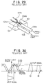
Incidentally, FIG. 29 is a perspective view of the
optical modulator 100 of a Mach-Zehnder type shown in
FIG. 28, looking from an outputting side thereof.
As shown in FIG. 28, the optical modulator 100
of a Mach-Zehnder type has an optical waveguide device
101 of a Mach-Zehnder type, a photo-detector 107 and a
signal controlling circuit (ABC circuit; automatic bias
control circuit) 108.
An optical waveguide 104 of a Mach-Zehnder type
is formed on a substrate 101a, further a travelling-wave
electrode 102 and a grounding electrode 103 are formed
on the optical waveguide 104, whereby the optical
waveguide device 101 of a Mach-Zehnder type is formed.
The optical waveguide 104 of a Mach-Zehnder type
has an input waveguide 104a, an output waveguide 104b,
and intermediate waveguides 104c and 104d. The
intermediate waveguides 104c and 104d are disposed in
parallel, and connected to the input waveguide 104a and
the output waveguide 104b at a Y-shaped splitting
portion Q1 and a Y-shaped recombining portion Q2.
The travelling-wave electrode 102 and the
grounding electrode 103 are used to control light
propagated in the optical waveguide 104, which are
respectively formed on the intermediate waveguides 104c
and 104d of the optical waveguide 104, as shown in FIG.
28.
Into the input waveguide 104a of the optical
waveguide 104, direct-current light emitted from a
semiconductor laser 111 is inputted through an optical
fiber 105a. From the output waveguide 104b of the
optical waveguide 104, modulated signal light is
outputted to a photo-detector 112 through an optical
fiber 105b.
The photo-detector 112 receives the signal light
outputted through the optical fiber 105b to convert it
into an electric signal.
An optical fiber 106 is directly attached, in
addition to the above-mentioned optical fiber 105b, onto
an end surface on the outputting side of the substrate
101a, through which radiation light (monitor light)
generated at the Y-shaped recombining portion Q2 of the
optical waveguide 104 is inputted to the photo-detector
107.
The photo-detector 107 receives the radiation
light inputted through the optical fiber 106 to convert
the received radiation light into an electric signal,
and outputs the electric signal to the signal
controlling circuit 108, thereby monitoring the
radiation light.
The photo-detector 107 is connected to the
signal controlling circuit 108, which varies direct-current
bias of an inputted electric signal to be
applied to the travelling-wave electrode 102 according
to a result of the monitoring by the photo-detector 107
(that is, according to a change of a light output
electric signal from the photo-detector 107).
In general, in the optical modulator 100 of a
Mach-Zehnder type, an operating point of the optical
modulator 100 of a Mach-Zehnder type is shifted with
time elapsed due to temperature drift, DC drift, stress
and the like.
Now, shift of the operating point of the optical
modulator 100 of a Mach-Zehnder type will be explained
with reference to FIG. 30.
FIG. 30 is a diagram showing an input-output
characteristic of the optical modulator 100 of a Mach-Zehnder
type. In FIG. 30, 1 ○ indicates the
characteristic before the operating point is shifted,
and 2 ○ indicates the characteristic in the case where the
operating point has been shifted.
As shown in FIG. 30, the input-output
characteristic of the optical modulator 100 of a Mach-Zehnder
type has periodicity to a driving voltage.
Use of driving voltages V⊘ and V1 at which an
upper peak value and a lower peak value of an output
light power are obtained according to a logical
multiplication of an input signal enables efficient
binary modulation.
However, if the driving voltages V⊘ and V1 are
constant even in the case where the operating point is
shifted, an extinction ratio of a signal light outputted
from the optical modulator 100 of a Mach-Zehnder type is
degraded because of the above-mentioned periodicity as
shown in FIG. 30.
When the operating point is shifted, it is
therefore necessary to control the operating point
assuming the driving voltages V⊘ and V1 as (V⊘ + dV) and
(V1 + dV), respectively, if a quantity of the shift is
dV.
In the optical modulator 100 of a Mach-Zehnder
type shown in FIG. 28, the photo-detector 107 monitors
radiation light generated at the Y-shaped recombining
portion Q2 of the optical waveguide 104, the signal
controlling circuit 108 varies direct-current bias of an
input electric signal to be applied to the travelling-wave
electrode 102, whereby the operating point of the
optical modulator 100 of a Mach-Zehnder type is
controlled.
Incidentally, reference numeral 109 denotes an
input signal source, and reference numeral 110 denotes a
termination resistor.
In the optical modulator 100 of a Mach-Zehnder
type with the above structure shown in FIG. 28, direct-current
light (incident light) from the semiconductor
laser 111 is inputted to the input waveguide 104a of the
optical waveguide 104 through the optical fiber 105a,
split into two at the Y-shaped splitting portion Q1 ,
then propagated in the intermediate waveguides 104c and
104d.
If a high-frequency modulating signal voltage is
applied to the travelling-wave electrode 102 at this
time, a phase difference is generated between the split
incident lights by the electrooptic effect in the
intermediate waveguides 104c and 104d, and the incident
lights whose phases are different are again combined at
the Y-shaped recombining portion Q2.
By setting the driving voltages at this time
such that the phase difference between the incident
lights in the intermediate waveguides 104c and 104d is 0
and π, an ON/OFF optical pulse signal can be obtained as
signal light to be outputted, and modulated signal light
is outputted from the output waveguide 104b of the
optical waveguide 104.
The signal light outputted from the output
waveguide 104b is received by the photo-detector 112
through the optical fiber 105b to be converted into an
electric signal.
On the other hand, the radiation light generated
at the Y-shaped recombining portion Q2 of the optical
waveguide 104 is received by the photo-detector 107
through the optical fiber 106, converted into an
electric signal, then outputted to the signal
controlling circuit 108.
The signal controlling circuit 108 varies
direct-current bias of the input electric signal to be
applied to the travelling-wave electrode 102 according
to a change of the light output electric signal from the
photo-detector 107, thereby controlling the operating
point of the optical modulator 100 of a Mach-Zehnder
type.
As above, the optical modulator 100 of a Mach-Zehnder
type shown in FIG. 28 can stabilize the
operating point thereof so as to prevent degradation of
signal light as shown in FIG. 30, and thus enables
stable optical modulation.
The optical modulator 100 of a Mach-Zehnder type
shown in FIG. 28 has, however, disadvantages that it is
necessary to align the optical fiber 106 for monitoring
since the optical fiber 106 is used when the radiation
light generated at the Y-shaped recombining portion Q2
of the light waveguide 104 is monitored, and thus there
is a difficulty in designing the mechanism.
Namely, the optical fiber 105b to which
modulated signal light is inputted and the optical fiber
106 to which radiation light generated at the Y-shaped
recombining portion Q2 of the light waveguide 104 is
inputted are spaced only about 80 µm apart so that
fabrication of the optical modulator 100 of a Mach-Zehnder
type is difficult.
For this, there has been also proposed an
optical modulator 100A of a Mach-Zehnder type without
the optical fiber 106 for monitoring, as shown in FIG.
31.
FIG. 32 is a side view of an outputting side of
an optical waveguide device 100A of a Mach-Zehnder type
shown in FIG. 31.
Namely, the optical modulator 100A of a Mach-Zehnder
type shown in FIG. 31 is directly arranged a
photo-detector 107 in the rear stage of an end surface
on an outputting side of a substrate 101a to directly
receive radiation light emitted from the end surface on
the outputting side of the substrate 101a by the photo-detector
107.
In FIG. 31, like reference characters designate
like or corresponding parts or functions of the optical
modulator 100 of a Mach-Zehnder type in FIG. 28.
In FIG. 31, reference numeral 113 denotes an
optical fiber to which direct-current light from a
semiconductor laser (not shown in FIG. 31) is inputted,
reference numeral 114 denotes a lens for condensing
incident light from the optical fiber 113, reference
numeral 115 denotes a lens for condensing signal light
emitted from an output waveguide 104b of an optical
waveguide 104, and reference numeral 116 denotes an
optical fiber for outputting the signal light from the
lens 115.
In the optical modulators 100 and 100A of a
Mach-Zehnder type shown in FIGS. 28 and 31,
respectively, radiation light generated at the Y-shaped
recombining portion Q2 of the optical waveguide 104 is
uniformly emitted to the vicinity of the Y-shaped
recombining portion Q2 so that an intensity of the
radiation light emitted from the end surface on the
outputting side of the substrate 101a is small, and thus
it is difficult to stably control the operating point of
the optical modulator.
SUMMARY OF THE INVENTION
In the light of the above problems, an object of
the present invention is to provide an optical modulator
which can adjust a position on the end surface on the
outputting side of the substrate to which monitor light
is emitted and increase an intensity of the monitor
light, thereby stably controlling the operating point of
the optical modulator while facilitating a design of the
mechanism.
The present invention therefore provide an
optical modulator comprising a substrate having
electrooptic effect, an optical waveguide of a Mach-Zehnder
type formed on the substrate, an electrode
formed on the substrate to control light propagated in
the optical waveguide, a light guiding unit for guiding
light radiated or leaking from the optical waveguide,
and an interference light generating means for making
light emitted from the light guiding unit and signal
light leaking from the optical waveguide interfere with
each other to generate interference light, and emitting
the interference light from an end surface of the
substrate.
The optical modulator according to this
invention further comprises a photo-detector for
monitoring the interference light obtained by the
interference light generating means, and a signal
controlling circuit for varying direct-current bias to
be applied to the electrode according to a change of the
interference light monitored by the photo-detector to
control an operating point of the optical modulator.
A refractive index of the light guiding unit is
such set as to differ from a refractive index of the
substrate.
The light guiding unit may guide radiation light
radiated from the optical waveguide, or guide radiation
light radiated from the optical waveguide and the signal
light leaking from the optical waveguide
Further, the light guiding unit may be provided
in the vicinity of an outputting-side optical waveguide
forming the optical waveguide, or provided in the
vicinity of an outputting-side optical waveguide with a
recombining portion having the recombining port ton
forming the optical waveguide and the outputting-side
optical waveguide forming the optical waveguide and
connected to the recombining portion.
The light guiding unit may be formed as a light
guiding unit fabricated by titanium diffusion, or as a
light guiding unit fabricated by ion exchange.
The outputting-side optical waveguide may be a
linear optical waveguide, or a curved optical waveguide
having a curved portion.
The interference light may be such set as to
have an inverted phase of the signal light.
The photo-detector may be disposed between the
end surface of the substrate and a lens disposed in a
front stage of an optical fiber for outputting, or
disposed in a rear stage of the end surface of the
substrate to which an optical fiber for outputting is
coupled.
The photo-detector may be formed by placing a
photo-detecting element on a plate member. At this
time, the plate member may be a ceramic substrate, and
the photo-detecting element may be a bear chip.
The substrate may be a lithium niobate
substrate.
The optical modulator according to this
invention guides light radiated or leaking from the
optical waveguide by the light guiding unit, and makes
light emitted from the light guiding unit and signal
light leaking from the optical waveguide interfere with
each other to generate interference light, thereby
increasing an intensity of monitor light emitted from
the end surface on the outputting side of the substrate
while adjusting a position on the end surface on the
outputting side of the substrate to which the
interference light as the monitor light is emitted.
Whereby, it is possible to dispose the optical
fiber to which modulated signal light is inputted and
the photo-detector receiving interference light a
desired distance apart. As a result, designing of a
mechanism of the optical modulator becomes easy and an
operating point control in the optical modulator becomes
stable so that it is possible to prevent degradation of
an extinction ratio of signal light due to a shift of
the operating point of the optical modulator, and thus
enable stable optical modulation.
If the light guiding unit is provided in the
vicinity of the outputting-side optical waveguide with a
recombining portion having the recombining portion
forming the optical waveguide and the outputting-side
optical waveguide forming the optical waveguide and
connected to the recombining portion, it is possible to
further increase condensation of light radiated or
leaking from the optical waveguide.
If the ouptutting-side optical waveguide is
formed by a curved optical waveguide having a curved
portion, it is possible to prevent light emitted from
the end surface on the outputting side of the substrate
from coming again into the intermediate waveguides and
the like of the optical waveguide.
BRIEF DESCRIPTION OF THE DRAWINGS
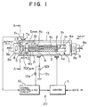
FIG. 1 is a schematic view of an optical
modulator according to an embodiment of this invention;
FIG. 2 is a sectional view of the optical
modulator shown in FIG. 1 taken along line A-A;
FIG. 3 is a perspective view of the optical
modulator shown in FIG. 1 looking into an emitting side
from an inputting side thereof;
FIG. 4 is a schematic view of an essential
structure of the optical modulator according to the
embodiment of this invention;
FIG. 5 is a side view of an outputting side of
an optical waveguide device of a Mach-Zehnder type in
the optical modulator shown in FIG. 4;
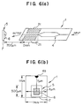
FIGS. 6(a) and 6(b) are diagrams for
illustrating a position in which a photo-detector is
disposed;
FIG. 7 is a diagram showing the photo-detector
shown in FIG. 6(b);
FIGS. 8(a) through 8(c) are diagrams for
illustrating a proton exchanging process;
FIGS. 9(a) through 9(c) are diagrams for
illustrating shapes of a light guiding region;
FIGS. 10(a) through 10(c) are diagrams for
illustrating positions of the light guiding region;
FIG. 11 is a diagram for illustrating a shape of
an output waveguide;
FIG. 12 is a diagram for illustrating signal
light and radiation light;
FIGS. 13(a) and 13(b) are diagrams for
illustrating the signal light and the radiation light;
FIG. 14 is a diagram for illustrating a
characteristic of an intensity of interference light;
FIG. 15 is a diagram for illustrating the
characteristic of the intensity of the interference
light;
FIG. 16 is a diagram for illustrating the
characteristic of the intensity of the interference
light;
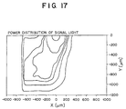
FIG. 17 is a diagram showing power distribution
of the signal light in the case where the light guiding
region is not provided;
FIG. 18 is a diagram showing power distribution
of the radiation light in the case where the light
guiding region is not provided;
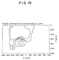
FIG. 19 is a diagram showing phase distribution
of the interference light in the case where the light
guiding region is not provided;
FIG. 20 is a diagram showing power distribution
of the signal light in the case where the light guiding
region is provided;
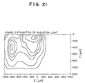
FIG. 21 is a diagram showing power distribution
of the radiation light in the case where the light
guiding region is provided;
FIG. 22 is a diagram showing phase distribution
of the interference light in the case where the light
guiding region is provided;
FIG. 23 is a diagram showing a result of a BPM
simulation in the case where the light guiding region is
not provided;
FIG. 24 is a diagram showing a result of the BPM
simulation in the case where the light guiding region is
provided;
FIG. 25 is a diagram showing a result of the BPM
simulation in the case where the light guiding region is
provided;
FIG. 26 is a schematic view of a modified
optical modulator according to the embodiment of this
invention;
FIG. 27 is a sectional view of the optical
modulator shown in FIG. 26 taken along line B-B;
FIG. 28 is a schematic view of an example of an
optical modulator of a Mach-Zehnder type;
FIG. 29 is a perspective view of the optical
modulator of a Mach-Zehnder type shown in FIG. 28
looking from an outputting side thereof;
FIG. 30 is a diagram showing an input-output
characteristic of the optical modulator of a Mach-Zehnder
type;
FIG. 31 is a schematic view of another example
of the optical modulator of a Mach-Zehnder type; and
FIG. 32 is a side view of an outputting side of
an optical waveguide device of a Mach-Zehnder type in
the optical modulator shown in FIG. 31.
DESCRIPTION OF THE PREFERRED EMBODIMENT
Hereinafter, an embodiment of this invention
will be described with reference to the drawings.
(a) Description of an embodiment of the invention
FIG. 1 is a schematic view of an optical
modulator according to an embodiment of this invention.
The optical modulator shown in FIG. 1 is an
optical modulator of a Mach-Zehnder type in a system
coupled via lenses, which is used as an external optical
modulator for modulating light emitted from a signal
light source such as a semiconductor laser or the like
in a transmitting unit of, for example, an ultra high-speed
optical communication system.
FIG. 2 is a sectional view of the optical
modulator 20 of a Mach-Zehnder type shown in FIG. 1
taken along line A-A. Fig. 3 is a perspective view of
the optical modulator 20 of a Mach-Zehnder type shown in
FIG. 1, looking into an emitting side from an inputting
side thereof.
FIG. 4 is a schematic view of an essential part
of the optical modulator 20 of a Mach-Zehnder type shown
in FIG. 1. FIG. 5 is a side view of an outputting side
of an optical waveguide device 1 of a Mach-Zehnder type
shown in FIG. 4.
FIGS. 6(a) and 6(b) are diagrams for
illustrating a position in which a photo-detector 5 is
disposed. FIG. 7 is the photo-detector 5 shown in FIG.
6(b).
As shown in FIG. 1, the optical modulator 20 of
a Mach-Zehnder type has a package 13 in which the
optical waveguide device (LN MOD) 1 of a Mach-Zehnder
type and the photo-detector 5 are incorporated, a driver
11 as an input signal source, and a signal controlling
circuit (ABC circuit; Automatic Bias Control Circuit)
10.
To an inputting side and an outputting side of
the package 13, optical fibers 9a and 9b are connected
via lens holders 8 each having a lens 8a used to
increase the condensation, respectively.
Incidentally, the driver 11 receives a pilot
signals from the signal controlling circuit 10 to input
data components in an inputted electric signal to the
optical waveguide device 1 of a Mach-Zehnder type.
Reference numeral 12a denotes an inductor, reference
numeral 12b denotes a capacitor and reference numeral
12c denotes a 50Ω terminating resistor.
An optical waveguide 4 of a Mach-Zehnder type is
formed on a substrate 1a, then a travelling-wave
electrode 2 and a grounding electrode 3 are formed on
the optical waveguide 4, whereby the optical waveguide
device 1 of a Mach-Zehnder type is formed.
A light guiding region 21 is provided in the
vicinity of the optical waveguide 4.
The substrate 1a is a lithium niobate (LiNbO3)
substrate (Z-cut substrate) having electrooptic effect.
The optical waveguide 4 of a Mach-Zehnder type
has an input waveguide 4a, an output waveguide 4b and
intermediate waveguides 4c and 4d. The intermediate
waveguides 4c and 4d are arranged in parallel and
connected to the input waveguide 4a and the output
waveguide 4b via a Y-shaped splitting portion R1 and a
Y-shaped recombining portion R2.
Direct-current light from a semiconductor laser
(not shown) is inputted to the input waveguide 4a of the
optical waveguide 4 through the optical fiber 9a
connected to the package 13, and modulated signal light
is outputted from the output waveguide 4b of the optical
waveguide 4 to the optical fiber 9b connected to the
package 13. Incidentally, the optical fiber 9a is a
constant polarization fiber, whereas the optical fiber
9b is a single-mode fiber.
A metal such as titanium (Ti) or the like in
thickness of 1000 Å is evaporated on a surface of the
lithium niobate (LiNbO3) substrate 1a, a pattern is
formed by photolithography and etching, and left for 8
hours in oxygen (in WetO2) at a high temperature of, for
example, 1000°C to diffuse the metal such as Ti or the
like into the substrate 1a in a titanium diffusing
process, whereby the optical waveguide 4 is formed.
Namely, a metal such as Ti or the like is
selectively diffused in only a part corresponding to the
optical waveguide 1 of the substrate 1a so that the part
has a larger refractive index than another part (the
substrate 1a), whereby the optical waveguide 4 is
formed.
On the optical waveguide 4, a buffer layer (not
shown) formed by a thin film consisting of silicon
dioxide (SiO2 ) or the like is formed in order to
decrease absorption of light by a metal electrode layer
(the travelling-wave electrode 2 and the grounding
electrode 3) on the optical waveguide 4.
To the buffer layer not shown, a coating (Si
coat) is applied by depositing silicon (Si), although
not shown, in order to improve stability of temperature
of the optical waveguide device 1 of a Mach-Zehnder
type.
The travelling-wave electrode 2 and the
grounding electrode 3 are used to control light
propagated in the optical waveguide 4, which are formed
by evaporating a metal such as gold (Au) or the like on
the intermediate waveguides 4c and 4d of the optical
waveguide 4.
The travelling-wave electrode 2 and the
grounding electrode 3 are connected to the input signal
source 11. The travelling-wave electrode 2 and the
grounding electrode 3 are applied thereto a voltage
according to an input signal (modulating wave signal)
from the input signal source 11 to vary a refractive
index of the intermediate waveguides 4c and 4d as will
be described later, thereby modulating direct-current
light inputted from the semiconductor laser (not shown)
through the optical fiber 9a.
The direct-current light from the semiconductor
laser is modulated by the travelling-wave electrode 2
and the grounding electrode 3, then outputted as signal
light (main signal light) or radiation light from the Y-shaped
recombining portion R2 of the optical waveguide
4.
The signal light and the radiation light have
inverse phases, as shown in FIG. 12. The signal light
and the radiation light have periodicity to a driving
voltage. In FIG. 12, the signal light is indicated by
reference character M, whereas the radiation light is
indicated by reference character N.
FIGS. 13(a) and 13(b) schematically show the
optical waveguide 4 of the optical waveguide device 1 of
a Mach-Zehnder type.
FIG. 13(a) shows a state of light propagation in
the case where no voltage is applied, whereas FIG. 13(b)
shows a state of light propagation in the case where a
voltage is applied.
In each of FIGS. 13(a) and 13(b), a propagation
mode is shown as a wave-like pattern in each of the
waveguides (the input waveguide 4a, the output waveguide
4b and the intermediate waveguides 4c and 4d) of the
optical waveguide 4.
In FIG. 13(a), the direct-current light from the
semiconductor laser not shown is split by the Y-shaped
splitting portion R1 when inputted to the input
waveguide 4a in a predetermined input mode, inputted to
the intermediate waveguides 4c and 4d, propagated in the
intermediate waveguides 4c and 4d in the same mode as
the input mode, recombined at the Y-shaped recombining
portion R2, and outputted from the output waveguide 4b
in the same mode.
In FIG. 13(b), the direct-current light from the
semiconductor laser not shown is split by the Y-shaped
splitting portion R1 when inputted to the input
waveguide 4a in a predetermined input mode, then
inputted to the intermediate waveguides 4c and 4d. In
this case, since a refractive index of the intermediate
waveguides 4c and 4d is changed because of an applied
voltage, a propagation velocity of the light is changed.
Therefore, a phase difference is generated in
the lights propagated in the intermediate waveguides 4c
and 4d. When the lights having different phases are
recombined at the Y-shaped recombining portion R2 , a
mode of light that should be inputted to the output
waveguide 4b differs from the input mode.
For this, the light reaching the Y-shaped
recombining portion R2 cannot be outputted to the output
waveguide 4b, and is thus radiated as radiation light to
the inside of the substrate 1a.
However, if the optical waveguide 4 is
fabricated under the above-mentioned conditions, the
signal light slightly leaks from the Y-shaped
recombining portion R2 to the inside of the substrate
1a.
The radiation light radiated from the Y-shaped
recombining portion R2 and a part of the signal light
leaking from the Y-shaped recombining portion R2 come
into the light guiding region 21 provided in the
vicinity of the optical waveguide 4 (that is, in the
vicinity of the both sides of the output waveguide 4b of
the optical waveguide 4, in concrete).
The light guiding region 21 guides the radiation
light radiated from the Y-shaped recombining portion R2
and the signal light leaking from the Y-shaped
recombining portion R2 such that the radiation light and
the signal light are not emitted from an end surface
other than an end surface on the outputting side of the
substrate 1a, which functions as a light guiding unit.
Namely, the light guiding region 21 guides light
coming into the light guiding region 21 to prevent
scattering of the coming light so as to increase an
intensity of monitor light emitted from the end surface
on the outputting side of the substrate 1a.
An intensity of the radiation light coming into
the light guiding region 21 is larger than an intensity
of the signal light coming into the light guiding region
21 so that the radiation light coming thereinto is
mainly guided in the light guiding region 21.
The light guiding region 21 is formed by
selectively diffusing a metal such as Ti or the like in
only a part corresponding to the light guiding region
portion in the substrate 1a in the titanium diffusing
process when the waveguide is formed, thereby having a
larger refractive index than another part (the substrate
1a), similarly to the optical waveguide 4 described
before.
The light guiding region 21 is provided in a
Position separated by about 7 to 10 µm from the output
waveguide 4b of the optical waveguide 4.
Actually, the travelling-wave electrode 2 is
also formed on the output waveguide 4b (not shown in
FIG. 1) in order to obtain wavelength chirp, whereby
phase modulation is conducted in the output waveguide 4b
in the optical modulator 20 of a Mach-Zehnder type.
For this, the travelling-wave electrode 2 is
also formed on the light guiding region 21 (not shown in
FIG. 1). However, since a voltage is also applied to
the light guiding region 21 by the travelling-wave
electrode 2 when the phase modulation is conducted, the
refractive index of the light guiding region 21 is
changed.
A change of the refractive index of the light
guiding region 21 exerts an effect on the signal light
leaking from the output waveguide 4b so that the
modulated waveform is degraded.
For this, the light guiding region 21 is
provided in a position separated by about 7 to 10 µm
from the output waveguide 4b.
A shorter length of the optical waveguide 21
allows a smaller gap between the output waveguide 4b and
the light guiding region 21.
The radiation light and the signal light
mentioned above coming into the light guiding region 21
interfere with each other within the light guiding
region 21, then are emitted from the light guiding
region 21 to the inside of the substrate 1a.
The light (the radiation light, mainly) emitted
from the light guiding region 21 further interferes with
the signal light leaking from the Y-shaped recombining
portion R2 when being propagated inside the substrate
1a, then is emitted as monitor light (interference
light) from the end surface on the outputting side of
the substrate 1a.
Namely, the substrate 1a in the vicinity of a
portion E of the output waveguide 4b functions as an
interference light generating means for making the light
emitted from the light guiding region 21 and the signal
light leaking from the Y-shaped recombining portion R2
interfere with each other to generate interference
light, and emitting the interference light from the end
surface on the outputting side of the substrate 1a.
Since the light guiding region 21 mainly guides
the radiation light as stated above, a phase of the
interference light emitted from the substrate 1a has an
inverted phase of the signal light. Incidentally,
setting of the phase of the interference light will be
described later.
As shown in FIG. 1, the photo-detector 5 is
disposed in the rear stage of the end surface on the
outputting side of the substrate 1a, and the signal
controlling circuit 10 is connected to a terminal T1 of
the photo-detector 5. A terminal T2 of the photo-detector
5 is grounded.
In concrete, the photo-detector 5 is interposed,
within the package 13, between the lens 8a arranged in
the front stage of the optical fiber 9b for outputting
and the end surface on the outputting side of the
substrate 1a of the optical waveguide device 1 of a
Mach-Zehnder type, as shown in FIG. 1.
As shown in FIGS. 1 through 3, the photo-detector
5 is formed by placing a bear chip 6 as a
photo-detecting element on a ceramic substrate 7. The
photo-detector 5 receives the monitor light
(interference light) emitted from the end surface on the
outputting side of the substrate 1a, converts the
received interference light into an electric signal, and
outputs the electric signal to the signal controlling
circuit 10, thereby monitoring the interference light.
An example of a size of the photo-detector 5 is shown in
FIG. 7. In FIG. 7, reference numeral 5a denotes an
electrode.
The signal controlling circuit 10 varies direct-current
bias of an input electric signal to be applied
to the travelling-wave electrode 2 according to a result
of the monitoring by the photo-detector 5 (that is, a
change of a light output electric signal from the photo-detector
5).
As stated above, in the optical modulator 20 of
a Mach-Zehnder type, an operating point of the optical
modulator 20 of a Mach-Zehnder type is generally shifted
with time elapsed due to temperature drift, DC drift,
stress and the like.
If optical modulation is conducted in a state
where the operating point has been shifted, the
extinction ratio is degraded as described before with
reference to FIG. 30.
Accordingly, the photo-detector 5 monitors the
interference light emitted from the end surface on the
outputting side of the substrate 1a, and the signal
controlling circuit 10 varies the direct-current bias of
the input electric signal to be applied to the
travelling-wave electrode 2 according to a result of the
monitoring by the photo-detector 5, whereby the
operating point of the optical modulator 20 of a Mach-Zehnder
type can be controlled.
In the optical modulator 20 of a Mach-Zehnder
type according to this embodiment, a phase of the
interference light is set such that the interference
light is emitted to a position separated by a desired
distance from an optical waveguide end position (an end
position of the output waveguide 4b of the optical
waveguide 4) on the end surface on the outputting side
of the substrate 1a.
In concrete, the photo-detector 5 is disposed in
a position several hundreds µm [this distance is
indicated by Y in FIG. 6(b), which is about 600 to 800
µm, for example] lower than the end position of the
output waveguide 4b on the end surface on the outputting
side of the substrate 1a in order to prevent the signal
light to be inputted to the optical fiber 9b from the
output waveguide 4b from being blocked.
The photo-detector 5 is disposed in a position
separated by several hundreds µm from the end surface on
the outputting side of the substrate 1a in order to
further widen a radiation region of the interference
light radiated from the end surface on the outputting
side of the substrate 1a, as shown in FIGS. 1 and 6(a).
FIGS. 1 and 6(a) show a case where the photo-detector 5
is disposed in a position separated by 700 µm from the
end surface on the outputting side of the substrate 1a.
A phase and an intensity of the interference
light is set by adjusting a fabrication condition of the
optical waveguide 4.
Namely, the phase and the intensity of the
interference light are set by varying a diffusion
condition upon fabricating the optical waveguide 4 as
the fabrication condition of the optical waveguide 4 so
as to adjust a signal light power (signal light
intensity) leaking from the Y-shaped recombining portion
R2 of the optical waveguide 4.
The phase and the intensity of the interference
light can be alternatively set by varying a length D of
the output waveguide 4b of the optical waveguide 4 [that
is, a length D from the Y-shaped recombining portion R2
of the optical waveguide 4 to the end surface on the
outputting side of the substrate 1a; refer to FIGS. 1
and 6(a)] as the fabrication condition of the optical
waveguide 4 so as to adjust the signal light power
leaking when propagated in the output waveguide 4b.
According to this embodiment, a length of the
output waveguide 4b is set to, for example, 4.5 mm or
more in order to allow the interference light to be
radiated on the entire of the end surface on the
outputting side of the substrate 1a.
In the optical modulator 20 of a Mach-Zehnder
type with the above structure according to this
embodiment, when direct-current light from the
semiconductor laser not shown is inputted to the package
13 through the optical fiber 9a, the incident light is
inputted to the optical waveguide 4 of the optical
waveguide device 1 of a Mach-Zehnder type.
In the optical waveguide device 1 of a Mach-Zehnder
type, the light inputted from the input
waveguide 4a is split by the Y-shaped splitting portion
R1 , modulated by the travelling-wave electrode 2 and the
grounding electrode 3 while being propagated in the
intermediate waveguides 4c and 4d, then the modulated
lights are recombined by the Y-shaped recombining
portion R2 of the optical waveguide 4.
Whereby, signal light and radiation light are
generated at the Y-shaped recombining portion R2 , and
the signal light is outputted from the output waveguide
4b, whereas the radiation light is radiated to the
inside of the substrate 1a from the Y-shaped recombining
portion R2 .
On the other hand, the signal light slightly
leaks from the Y-shaped recombining portion R2 to the
inside of the substrate 1a.
The radiation light and the leaking signal light
come into the light guiding region 21. The incident
light is guided by the light guiding region 21 while
being prevented from being scattered, then emitted to
the inside of the substrate 1a.
The light emitted from the light guiding region
21 interferes with the signal light leaking from the Y-shaped
recombining portion R2 when propagated inside the
substrate 1a, then emitted as interference light from
the end surface on the outputting side of the substrate
1a.
Since the phase of the interference light is set
by adjusting the fabrication condition of the optical
waveguide 4 at this time as stated before, the
interference light is emitted to a position separated by
a desired distance from the end position of the output
waveguide 4b on the end surface on the outputting side
of the substrate 1a.
The emitted interference light is received by
the photo-detector 5 disposed in a relevant position.
The photo-detector 5 converts the received interference
light into an electric signal, and outputs the electric
signal to the signal controlling circuit 10.
As a result, the signal controlling circuit 10
varies direct-current bias of the input electric signal
to be applied to the travelling-wave electrode 2
according to a change of the light output electric
signal from the photo-detector 5, thereby controlling
the operating point of the optical modulator 20 of a
Mach-Zehnder type.
The signal light outputted from the output
waveguide 4b of the optical waveguide device 1 of a
Mach-Zehnder type is outputted via the lens 8a to the
optical fiber 9b connected to the package 13.
Next, characteristics of the optical modulator
20 of a Mach-Zehnder type according to this embodiment
will be described with reference to FIGS. 14 through 25.
FIGS. 14 through 16 illustrate a characteristic
of interference light intensity. FIGS. 23 through 25
illustrate results of BPM (Beam Profile Method)
simulation.
FIGS. 17 and 20 illustrate power distribution of
signal light. FIG. 18 and 21 illustrate power
distribution of radiation light. FIGS. 19 and 22
illustrate phase distribution of interference light.
(1) In the case where the light guiding region 21 is
not provided in the vicinity of the output waveguide 4b:
FIGS. 17 and 18 show power distribution of the
signal light and power distribution of the radiation
light, respectively, in this case. From FIGS. 17 and
18, phase distribution of interference light is as shown
in FIG. 19.
Since an intensity of the radiation light is
small in this case, a phase of the interference light
has the same phase as the signal light.
As shown in FIG. 19, the interference light is
emitted to a position about 600 to 800 µm lower than the
end position of the output waveguide 4b on the end
surface on the outputting side of the substrate 1a.
In FIG. 23, a result of the BPM simulation in
this case is shown. FIG. 23 shows distribution of light
radiated or leaking from the Y-shaped recombining
portion R2 of the optical waveguide 4.
In this case, it is seen from FIG. 23 that the
light emitted from the Y-shaped recombining portion R2
is mostly emitted from end surfaces other than the end
surface on the outputting side of the substrate 1a. In
consequence, it is considered that monitor light
(interference light) emitted from the end surface on the
outputting side of the substrate 1a is scattered in an
appreciable extent.
(2) In the case where the light guiding region 21 is
provided in the vicinity of the output waveguide 4b:
FIGS. 20 and 21 show power distribution of the
signal light and power distribution of the radiation
light, respectively, in this case. From FIGS. 20 and
21, phase distribution of the interference light is as
shown in FIG. 22.
Since an intensity of the radiation light is
increased in this case, the interference light has an
inverted phase of the signal light.
As shown in FIG. 22, the interference light is
emitted to a position about 600 to 800 µm lower than the
end position of the output substrate 4b on the end
surface on the outputting side of the substrate 1a.
FIGS. 24 and 25 show results of the BPM
simulation in this case.
FIGS. 24 and 25 show distribution of light
radiated or leaking from the Y-shaped recombining
portion R2 of the light waveguide 4. In FIGS. 24 and
25, widths of the light guiding region 21 are 100 µm and
200 µm, respectively.
In this case, it is seen from FIGS. 24 and 25
that the light emitted from the Y-shaped recombining
portion R2 is guided in a direction of the end surface
on the outputting side of the substrate 1a by the light
guiding region 21. In consequence, it is considered
that it is possible to decrease scattering of the
monitor light (interference light) emitted from the end
surface on the outputting side of the substrate 1a.
If a width of the light guiding region 21 is
increased as shown in FIG. 25, it is possible to largely
decrease scattering of the light emitted from the Y-shaped
recombining portion R2 , and guide the radiation
light to a wide region on the end surface on the
outputting side of the substrate 1a.
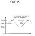
In FIG. 16, there are shown an example of an
interference light intensity RD C and RA C in the case
where the light guiding region 21 is provided by
reference character K2 , and an example of the
interference light intensity RD C and RA C in the case
where the light guiding region 21 is not provided by
reference character K1 .
If an average value of the light output electric
signals (current signals) from the photo-detector (PD) 5
is I
A V E , a difference between a peak value and a bottom
value of the light output electric signal is ΔI
O (refer
to FIGS. 14 and 15) and an output current from the
signal light source (LD MOD) 22 shown in FIG. 14 is P
i n ,
R
D C and R
A C are given by the following
equations 1 ○ and
2 ○, respectively:
By adjusting the interference light intensity
such that a ratio of RDC to RAC is small (that is, by
designing the optical modulator 20 of a Mach-Zehnder
type such that RDC is smaller and RAC is larger), it is
possible to improve the S/N ratio in the signal
controlling circuit 10 and stabilize the operating point
control of the optical modulator 20 of a Mach-Zehnder
type.
If the light guiding region 21 is provided, it
is possible to increase RA C as compared with a case
where the light guiding region 21 is not provided, as
shown in FIG. 16. It is therefore possible to improve
the S/N ratio in the signal controlling circuit 10 and
stabilize the operating point control in the optical
modulator 20 of a Mach-Zehnder type.
In FIGS. 17 through 22, X (µm) entered along the
horizontal axis and Y (µm) entered along the vertical
axis correspond to X and Y (Y corresponds to the
distance Y described before) shown in FIG. 6(b),
respectively.
In FIGS. 17 through 22, in order to show that
the distance Y mentioned above is a length in the
downward direction from the end position of the output
waveguide 4b on the end surface on the outputting side
of the substrate 1a, negative numeral values are
designated to Y entered along the vertical axis.
As to X entered along the horizontal axis, the
end position of the output waveguide 4b on the end
surface on the outputting side of the substrate 1a is
indicated by 0, a length in the rightward direction from
the end position of the output waveguide 4b is indicated
by a positive numeral value, whereas an a length in the
leftward direction is indicated by a negative numeral
value.
In FIGS. 17 through 22, power distribution of
the signal light, power distribution of the radiation
light, or phase distribution of the interference light
is asymmetric. A reason of this is that the optical
waveguide device 1 of a Mach-Zehnder type with the end
surface on the outputting side of the substrate 1a
obliquely cut when looked from the above is used in
order to diminish reflected feedback light of the
emitted light (refer to FIG. 1).
The optical modulator 20 of a Mach-Zehnder type
according to the embodiment of this invention guides
light radiated or leaking from the optical waveguide 4
by the light guiding region 21, besides using
interference light of the light emitted from light
guiding region 21 and signal light leaking from the
optical waveguide 4 as monitor light used when the
operating point is controlled, thereby increasing an
intensity of the monitor light (interference light)
emitted from the end surface on the outputting side of
the substrate 1a while adjusting a position on the end
surface on the outputting side of the substrate 1a to
which the monitor light is emitted.
It is therefore possible to dispose the optical
fiber 9b to which the modulated signal light is inputted
and the photo-detector 5 receiving the interference
light a desired distance apart. As a result, it becomes
unnecessary to provide an optical fiber for monitoring
(refer to reference numeral 106) as shown in FIG. 28,
and it is possible to facilitate a design of the
mechanism of the optical modulator 20 of a Mach-Zehnder
type.
Further, it is possible to stably control the
operating point of the optical modulator 20 of a Mach-Zehnder
type, which can prevent degradation of the
extinction ratio of the signal light due to shift of the
operating point of the optical modulator 20 of a Mach-Zehnder
type so as to enable stable optical modulation.
The photo-detector 5 is disposed in a position a
predetermined length (the distance Y) lower than the end
position of the output waveguide 4b on the end surface
on the outputting side of the substrate 1a. It is
thereby possible to prevent the signal light to be
outputted to the optical fiber 9b from the output
waveguide 4b of the optical waveguide 4 from being
blocked.
The photo-detector 5 is disposed in a position
separated by several hundreds µm (about 700 µm, for
example) from the end surface on the outputting side of
the substrate 1a. It is thereby possible to further
widen a radiation region of the interference light
emitted from the end surface on the outputting side of
the substrate 1a.
If the length D of the output waveguide 4b of
the optical waveguide 4 is set to, for example, 4.5 mm
or more, it is possible to radiate the interference
light on the entire of the end surface on the outputting
side of the substrate 1a so that the interference light
can be readily monitored by the photo-detector 5.
This embodiment has been described by way of an
example where a shape of the light guiding region 21 is
as shown in FIG. 9(a). However, the light guiding
region 21 may have a shape as shown in FIG. 9(b) or
9(c).
Particularly, if the light guiding region 21 has
a shape such that a width thereof is gradually narrowed
as getting closer to the end surface on the outputting
side of the substrate 1a as shown in FIG. 9(c), it is
possible to increase condensation of the light radiated
or leaking from the optical waveguide 4.
If the light guiding region 21 is provided in
the vicinity of an outputting-side waveguide with a
recombining portion formed by the Y-shaped recombining
portion R2 and the output waveguide 4b of the optical
waveguide 4, as shown in FIGS. 10(a) through 10(c), it
is possible to further increase condensation of light
radiated or leaking from the optical waveguide 4.
This embodiment has been described by way of an
example where the light guiding region 21 is provided on
the both sides of the output waveguide 4b. However, it
is alternatively possible to provide the light guiding
region 21 on only one side of the output waveguide 4b.
Further, this embodiment has been described by
way of an example where the light guiding region 21 is
formed in the titanium diffusing process to diffuse a
metal such as Ti in the substrate 1a. However, it is
alternatively possible to form the light guiding region
21 in an ion exchanging process.
Namely, a mask pattern of the light guiding
region 21 is formed on the substrate 1a [refer to FIG.
8(a)], then heat-treated with, for example,
pyrophosphoric acid to conduct a proton exchanging
process [refer to FIG. 8(b)], whereby the light guiding
region 21 may be formed.
A proportion of the proton exchange in the light
guiding region 21 can be adjusted by an annealing
process in oxygen (in O2) at a high temperature of 350° C
[refer to FIG. 8(c)].
The light waveguide 4 may be formed in the
proton exchanging process.
If the signal light can be prevented from
leaking from the optical waveguide 4 by changing the
fabrication condition of the optical waveguide 4, the
light guiding region 21 guides only the radiation light
radiated from the optical waveguide 4.
If the output waveguide 4b is formed by a curved
waveguide having a curved portion as shown in FIG. 11,
light emitted from the end surface on the outputting
side of the substrate 1a can be prevented from again
coming into the intermediate waveguides 4c and 4d, and
the like.
(b) Description of modification of the embodiment of
the invention
FIG. 26 is a schematic view of a modified
optical modulator according to the embodiment of this
invention.
The optical modulator shown in FIG. 26 is an
optical modulator of a Mach-Zehnder type in a fiber
direct-connect system. Similarly to the optical
modulator shown in FIG. 1, the optical modulator shown
in FIG. 26 is used, in a transmitting unit of, for
example, an ultra high-speed optical communication
system, as an external optical modulator for modulating
light emitted from a signal light source such as a
semiconductor laser or the like.
FIG. 27 is a sectional view of the optical
modulator 20A of a Mach-Zehnder type shown in FIG. 26
taken along line B-B.
The optical modulator 20A of a Mach-Zehnder type
shown in FIG. 26 is formed similarly to the optical
modulator 20 of a Mach-Zehnder type shown in FIG. 1,
excepting that the optical fibers 9a and 9b are directly
connected to the optical waveguide device 1 of a Mach-Zehnder
type within the package 13.
Namely, there are formed two holes H in the
package 13, into which the optical fibers 9a and 9b are
inserted, as shown in FIG. 26.
A tip of the optical fiber 9a is fixed to an end
of the input waveguide 4a on the end surface on the
inputting side of the substrate 1a of the optical
waveguide device 1 of a Mach-Zehnder type, whereas a tip
of the optical fiber 9b is fixed to an end of the output
waveguide 4b on the end surface on the outputting side
of the substrate 1a of the optical waveguide device 1 of
a Mach-Zehnder type, both with an adhesive C or the
like.
In this case, the photo-detector 5 is disposed
in the rear stage of the end surface on the outputting
side of the substrate 1a to which the optical fiber 9b
is connected, below the optical fiber 9b, as shown in
FIGS. 26 and 27.
The optical modulator 20A of the Mach-Zehnder
type may achieve the same functions and effects as the
above-described optical modulator 20 of a Mach-Zehnder
type according to the embodiment.
In particular, since the optical modulator 20A
of a Mach-Zehnder type is in a fiber direct-connect
system, the phase of the interference light is
arbitrarily set, and optical fiber 9b and the photo-detector
5 are disposed a desired distance apart,
whereby the optical modulator 20A of a Mach-Zehnder type
may be readily fabricated.
In the optical modulator 20A of a Mach-Zehnder
type, it is possible to provide the light guiding region
21 on only one side of the output waveguide 4b, as well.