EP0859263A2 - Optical modulator - Google Patents
Optical modulator Download PDFInfo
- Publication number
- EP0859263A2 EP0859263A2 EP97113223A EP97113223A EP0859263A2 EP 0859263 A2 EP0859263 A2 EP 0859263A2 EP 97113223 A EP97113223 A EP 97113223A EP 97113223 A EP97113223 A EP 97113223A EP 0859263 A2 EP0859263 A2 EP 0859263A2
- Authority
- EP
- European Patent Office
- Prior art keywords
- light
- optical waveguide
- optical
- optical modulator
- substrate
- Prior art date
- Legal status (The legal status is an assumption and is not a legal conclusion. Google has not performed a legal analysis and makes no representation as to the accuracy of the status listed.)
- Granted
Links
Images


Classifications
-
- G—PHYSICS
- G02—OPTICS
- G02F—OPTICAL DEVICES OR ARRANGEMENTS FOR THE CONTROL OF LIGHT BY MODIFICATION OF THE OPTICAL PROPERTIES OF THE MEDIA OF THE ELEMENTS INVOLVED THEREIN; NON-LINEAR OPTICS; FREQUENCY-CHANGING OF LIGHT; OPTICAL LOGIC ELEMENTS; OPTICAL ANALOGUE/DIGITAL CONVERTERS
- G02F1/00—Devices or arrangements for the control of the intensity, colour, phase, polarisation or direction of light arriving from an independent light source, e.g. switching, gating or modulating; Non-linear optics
- G02F1/01—Devices or arrangements for the control of the intensity, colour, phase, polarisation or direction of light arriving from an independent light source, e.g. switching, gating or modulating; Non-linear optics for the control of the intensity, phase, polarisation or colour
- G02F1/0121—Operation of devices; Circuit arrangements, not otherwise provided for in this subclass
- G02F1/0123—Circuits for the control or stabilisation of the bias voltage, e.g. automatic bias control [ABC] feedback loops
-
- G—PHYSICS
- G02—OPTICS
- G02F—OPTICAL DEVICES OR ARRANGEMENTS FOR THE CONTROL OF LIGHT BY MODIFICATION OF THE OPTICAL PROPERTIES OF THE MEDIA OF THE ELEMENTS INVOLVED THEREIN; NON-LINEAR OPTICS; FREQUENCY-CHANGING OF LIGHT; OPTICAL LOGIC ELEMENTS; OPTICAL ANALOGUE/DIGITAL CONVERTERS
- G02F1/00—Devices or arrangements for the control of the intensity, colour, phase, polarisation or direction of light arriving from an independent light source, e.g. switching, gating or modulating; Non-linear optics
- G02F1/01—Devices or arrangements for the control of the intensity, colour, phase, polarisation or direction of light arriving from an independent light source, e.g. switching, gating or modulating; Non-linear optics for the control of the intensity, phase, polarisation or colour
- G02F1/21—Devices or arrangements for the control of the intensity, colour, phase, polarisation or direction of light arriving from an independent light source, e.g. switching, gating or modulating; Non-linear optics for the control of the intensity, phase, polarisation or colour by interference
- G02F1/225—Devices or arrangements for the control of the intensity, colour, phase, polarisation or direction of light arriving from an independent light source, e.g. switching, gating or modulating; Non-linear optics for the control of the intensity, phase, polarisation or colour by interference in an optical waveguide structure
-
- G—PHYSICS
- G02—OPTICS
- G02F—OPTICAL DEVICES OR ARRANGEMENTS FOR THE CONTROL OF LIGHT BY MODIFICATION OF THE OPTICAL PROPERTIES OF THE MEDIA OF THE ELEMENTS INVOLVED THEREIN; NON-LINEAR OPTICS; FREQUENCY-CHANGING OF LIGHT; OPTICAL LOGIC ELEMENTS; OPTICAL ANALOGUE/DIGITAL CONVERTERS
- G02F2201/00—Constructional arrangements not provided for in groups G02F1/00 - G02F7/00
- G02F2201/58—Arrangements comprising a monitoring photodetector
-
- G—PHYSICS
- G02—OPTICS
- G02F—OPTICAL DEVICES OR ARRANGEMENTS FOR THE CONTROL OF LIGHT BY MODIFICATION OF THE OPTICAL PROPERTIES OF THE MEDIA OF THE ELEMENTS INVOLVED THEREIN; NON-LINEAR OPTICS; FREQUENCY-CHANGING OF LIGHT; OPTICAL LOGIC ELEMENTS; OPTICAL ANALOGUE/DIGITAL CONVERTERS
- G02F2203/00—Function characteristic
- G02F2203/21—Thermal instability, i.e. DC drift, of an optical modulator; Arrangements or methods for the reduction thereof
Definitions
- the present invention relates to an optical modulator suitable for use as an external optical modulator for modulating light emitted from a signal light source, in a transmitting unit of, for example, an ultra high-speed optical communication system.
- an optical modulator in a direct modulation system which modulates an electric current flowing in a semiconductor laser with a data signal, as an optical modulator which modulates light emitted from, for example, a semiconductor laser as a signal source.
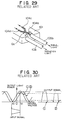
- FIG. 29 is a perspective view of the optical modulator 100 of a Mach-Zehnder type shown in FIG. 28, looking from an outputting side thereof.
- the optical modulator 100 of a Mach-Zehnder type has an optical waveguide device 101 of a Mach-Zehnder type, a photo-detector 107 and a signal controlling circuit (ABC circuit; automatic bias control circuit) 108.
- ABSC circuit automatic bias control circuit
- An optical waveguide 104 of a Mach-Zehnder type is formed on a substrate 101a, further a travelling-wave electrode 102 and a grounding electrode 103 are formed on the optical waveguide 104, whereby the optical waveguide device 101 of a Mach-Zehnder type is formed.
- the optical waveguide 104 of a Mach-Zehnder type has an input waveguide 104a, an output waveguide 104b, and intermediate waveguides 104c and 104d.
- the intermediate waveguides 104c and 104d are disposed in parallel, and connected to the input waveguide 104a and the output waveguide 104b at a Y-shaped splitting portion Q 1 and a Y-shaped recombining portion Q 2 .
- the travelling-wave electrode 102 and the grounding electrode 103 are used to control light propagated in the optical waveguide 104, which are respectively formed on the intermediate waveguides 104c and 104d of the optical waveguide 104, as shown in FIG. 28.
- direct-current light emitted from a semiconductor laser 111 is inputted through an optical fiber 105a.
- modulated signal light is outputted to a photo-detector 112 through an optical fiber 105b.
- the photo-detector 112 receives the signal light outputted through the optical fiber 105b to convert it into an electric signal.
- An optical fiber 106 is directly attached, in addition to the above-mentioned optical fiber 105b, onto an end surface on the outputting side of the substrate 101a, through which radiation light (monitor light) generated at the Y-shaped recombining portion Q 2 of the optical waveguide 104 is inputted to the photo-detector 107.
- the photo-detector 107 receives the radiation light inputted through the optical fiber 106 to convert the received radiation light into an electric signal, and outputs the electric signal to the signal controlling circuit 108, thereby monitoring the radiation light.
- the photo-detector 107 is connected to the signal controlling circuit 108, which varies direct-current bias of an inputted electric signal to be applied to the travelling-wave electrode 102 according to a result of the monitoring by the photo-detector 107 (that is, according to a change of a light output electric signal from the photo-detector 107).
- an operating point of the optical modulator 100 of a Mach-Zehnder type is shifted with time elapsed due to temperature drift, DC drift, stress and the like.
- FIG. 30 is a diagram showing an input-output characteristic of the optical modulator 100 of a Mach-Zehnder type.
- 1 ⁇ indicates the characteristic before the operating point is shifted
- 2 ⁇ indicates the characteristic in the case where the operating point has been shifted.
- the input-output characteristic of the optical modulator 100 of a Mach-Zehnder type has periodicity to a driving voltage.
- the photo-detector 107 monitors radiation light generated at the Y-shaped recombining portion Q 2 of the optical waveguide 104, the signal controlling circuit 108 varies direct-current bias of an input electric signal to be applied to the travelling-wave electrode 102, whereby the operating point of the optical modulator 100 of a Mach-Zehnder type is controlled.
- reference numeral 109 denotes an input signal source
- reference numeral 110 denotes a termination resistor
- direct-current light (incident light) from the semiconductor laser 111 is inputted to the input waveguide 104a of the optical waveguide 104 through the optical fiber 105a, split into two at the Y-shaped splitting portion Q 1 , then propagated in the intermediate waveguides 104c and 104d.
- an ON/OFF optical pulse signal can be obtained as signal light to be outputted, and modulated signal light is outputted from the output waveguide 104b of the optical waveguide 104.
- the signal light outputted from the output waveguide 104b is received by the photo-detector 112 through the optical fiber 105b to be converted into an electric signal.
- the radiation light generated at the Y-shaped recombining portion Q 2 of the optical waveguide 104 is received by the photo-detector 107 through the optical fiber 106, converted into an electric signal, then outputted to the signal controlling circuit 108.
- the signal controlling circuit 108 varies direct-current bias of the input electric signal to be applied to the travelling-wave electrode 102 according to a change of the light output electric signal from the photo-detector 107, thereby controlling the operating point of the optical modulator 100 of a Mach-Zehnder type.
- the optical modulator 100 of a Mach-Zehnder type shown in FIG. 28 can stabilize the operating point thereof so as to prevent degradation of signal light as shown in FIG. 30, and thus enables stable optical modulation.
- the optical modulator 100 of a Mach-Zehnder type shown in FIG. 28 has, however, disadvantages that it is necessary to align the optical fiber 106 for monitoring since the optical fiber 106 is used when the radiation light generated at the Y-shaped recombining portion Q 2 of the light waveguide 104 is monitored, and thus there is a difficulty in designing the mechanism.
- the optical fiber 105b to which modulated signal light is inputted and the optical fiber 106 to which radiation light generated at the Y-shaped recombining portion Q 2 of the light waveguide 104 is inputted are spaced only about 80 ⁇ m apart so that fabrication of the optical modulator 100 of a Mach-Zehnder type is difficult.
- FIG. 32 is a side view of an outputting side of an optical waveguide device 100A of a Mach-Zehnder type shown in FIG. 31.
- the optical modulator 100A of a Mach-Zehnder type shown in FIG. 31 is directly arranged a photo-detector 107 in the rear stage of an end surface on an outputting side of a substrate 101a to directly receive radiation light emitted from the end surface on the outputting side of the substrate 101a by the photo-detector 107.
- like reference characters designate like or corresponding parts or functions of the optical modulator 100 of a Mach-Zehnder type in FIG. 28.
- reference numeral 113 denotes an optical fiber to which direct-current light from a semiconductor laser (not shown in FIG. 31) is inputted
- reference numeral 114 denotes a lens for condensing incident light from the optical fiber 113
- reference numeral 115 denotes a lens for condensing signal light emitted from an output waveguide 104b of an optical waveguide 104
- reference numeral 116 denotes an optical fiber for outputting the signal light from the lens 115.
- radiation light generated at the Y-shaped recombining portion Q 2 of the optical waveguide 104 is uniformly emitted to the vicinity of the Y-shaped recombining portion Q 2 so that an intensity of the radiation light emitted from the end surface on the outputting side of the substrate 101a is small, and thus it is difficult to stably control the operating point of the optical modulator.
- an object of the present invention is to provide an optical modulator which can adjust a position on the end surface on the outputting side of the substrate to which monitor light is emitted and increase an intensity of the monitor light, thereby stably controlling the operating point of the optical modulator while facilitating a design of the mechanism.
- the present invention therefore provide an optical modulator comprising a substrate having electrooptic effect, an optical waveguide of a Mach-Zehnder type formed on the substrate, an electrode formed on the substrate to control light propagated in the optical waveguide, a light guiding unit for guiding light radiated or leaking from the optical waveguide, and an interference light generating means for making light emitted from the light guiding unit and signal light leaking from the optical waveguide interfere with each other to generate interference light, and emitting the interference light from an end surface of the substrate.
- the optical modulator according to this invention further comprises a photo-detector for monitoring the interference light obtained by the interference light generating means, and a signal controlling circuit for varying direct-current bias to be applied to the electrode according to a change of the interference light monitored by the photo-detector to control an operating point of the optical modulator.
- a refractive index of the light guiding unit is such set as to differ from a refractive index of the substrate.
- the light guiding unit may guide radiation light radiated from the optical waveguide, or guide radiation light radiated from the optical waveguide and the signal light leaking from the optical waveguide
- the light guiding unit may be provided in the vicinity of an outputting-side optical waveguide forming the optical waveguide, or provided in the vicinity of an outputting-side optical waveguide with a recombining portion having the recombining port ton forming the optical waveguide and the outputting-side optical waveguide forming the optical waveguide and connected to the recombining portion.
- the light guiding unit may be formed as a light guiding unit fabricated by titanium diffusion, or as a light guiding unit fabricated by ion exchange.
- the outputting-side optical waveguide may be a linear optical waveguide, or a curved optical waveguide having a curved portion.
- the interference light may be such set as to have an inverted phase of the signal light.
- the photo-detector may be disposed between the end surface of the substrate and a lens disposed in a front stage of an optical fiber for outputting, or disposed in a rear stage of the end surface of the substrate to which an optical fiber for outputting is coupled.
- the photo-detector may be formed by placing a photo-detecting element on a plate member.
- the plate member may be a ceramic substrate
- the photo-detecting element may be a bear chip.
- the substrate may be a lithium niobate substrate.
- the optical modulator according to this invention guides light radiated or leaking from the optical waveguide by the light guiding unit, and makes light emitted from the light guiding unit and signal light leaking from the optical waveguide interfere with each other to generate interference light, thereby increasing an intensity of monitor light emitted from the end surface on the outputting side of the substrate while adjusting a position on the end surface on the outputting side of the substrate to which the interference light as the monitor light is emitted.
- the light guiding unit is provided in the vicinity of the outputting-side optical waveguide with a recombining portion having the recombining portion forming the optical waveguide and the outputting-side optical waveguide forming the optical waveguide and connected to the recombining portion, it is possible to further increase condensation of light radiated or leaking from the optical waveguide.
- the ouptutting-side optical waveguide is formed by a curved optical waveguide having a curved portion, it is possible to prevent light emitted from the end surface on the outputting side of the substrate from coming again into the intermediate waveguides and the like of the optical waveguide.
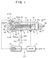
- FIG. 1 is a schematic view of an optical modulator according to an embodiment of this invention.
- the optical modulator shown in FIG. 1 is an optical modulator of a Mach-Zehnder type in a system coupled via lenses, which is used as an external optical modulator for modulating light emitted from a signal light source such as a semiconductor laser or the like in a transmitting unit of, for example, an ultra high-speed optical communication system.
- FIG. 2 is a sectional view of the optical modulator 20 of a Mach-Zehnder type shown in FIG. 1 taken along line A-A.
- Fig. 3 is a perspective view of the optical modulator 20 of a Mach-Zehnder type shown in FIG. 1, looking into an emitting side from an inputting side thereof.
- FIG. 4 is a schematic view of an essential part of the optical modulator 20 of a Mach-Zehnder type shown in FIG. 1.
- FIG. 5 is a side view of an outputting side of an optical waveguide device 1 of a Mach-Zehnder type shown in FIG. 4.
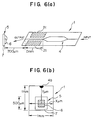
- FIGS. 6(a) and 6(b) are diagrams for illustrating a position in which a photo-detector 5 is disposed.
- FIG. 7 is the photo-detector 5 shown in FIG. 6(b).
- the optical modulator 20 of a Mach-Zehnder type has a package 13 in which the optical waveguide device (LN MOD) 1 of a Mach-Zehnder type and the photo-detector 5 are incorporated, a driver 11 as an input signal source, and a signal controlling circuit (ABC circuit; Automatic Bias Control Circuit) 10.
- LN MOD optical waveguide device
- ABS Automatic Bias Control Circuit
- optical fibers 9a and 9b are connected via lens holders 8 each having a lens 8a used to increase the condensation, respectively.
- the driver 11 receives a pilot signals from the signal controlling circuit 10 to input data components in an inputted electric signal to the optical waveguide device 1 of a Mach-Zehnder type.
- Reference numeral 12a denotes an inductor
- reference numeral 12b denotes a capacitor
- reference numeral 12c denotes a 50 ⁇ terminating resistor.
- An optical waveguide 4 of a Mach-Zehnder type is formed on a substrate 1a, then a travelling-wave electrode 2 and a grounding electrode 3 are formed on the optical waveguide 4, whereby the optical waveguide device 1 of a Mach-Zehnder type is formed.
- a light guiding region 21 is provided in the vicinity of the optical waveguide 4.
- the substrate 1a is a lithium niobate (LiNbO 3 ) substrate (Z-cut substrate) having electrooptic effect.
- the optical waveguide 4 of a Mach-Zehnder type has an input waveguide 4a, an output waveguide 4b and intermediate waveguides 4c and 4d.
- the intermediate waveguides 4c and 4d are arranged in parallel and connected to the input waveguide 4a and the output waveguide 4b via a Y-shaped splitting portion R 1 and a Y-shaped recombining portion R 2 .
- Direct-current light from a semiconductor laser (not shown) is inputted to the input waveguide 4a of the optical waveguide 4 through the optical fiber 9a connected to the package 13, and modulated signal light is outputted from the output waveguide 4b of the optical waveguide 4 to the optical fiber 9b connected to the package 13.
- the optical fiber 9a is a constant polarization fiber
- the optical fiber 9b is a single-mode fiber.
- a metal such as titanium (Ti) or the like in thickness of 1000 ⁇ is evaporated on a surface of the lithium niobate (LiNbO 3 ) substrate 1a, a pattern is formed by photolithography and etching, and left for 8 hours in oxygen (in WetO 2 ) at a high temperature of, for example, 1000°C to diffuse the metal such as Ti or the like into the substrate 1a in a titanium diffusing process, whereby the optical waveguide 4 is formed.
- a metal such as Ti or the like is selectively diffused in only a part corresponding to the optical waveguide 1 of the substrate 1a so that the part has a larger refractive index than another part (the substrate 1a), whereby the optical waveguide 4 is formed.
- a buffer layer (not shown) formed by a thin film consisting of silicon dioxide (SiO 2 ) or the like is formed in order to decrease absorption of light by a metal electrode layer (the travelling-wave electrode 2 and the grounding electrode 3) on the optical waveguide 4.
- a coating is applied by depositing silicon (Si), although not shown, in order to improve stability of temperature of the optical waveguide device 1 of a Mach-Zehnder type.
- the travelling-wave electrode 2 and the grounding electrode 3 are used to control light propagated in the optical waveguide 4, which are formed by evaporating a metal such as gold (Au) or the like on the intermediate waveguides 4c and 4d of the optical waveguide 4.
- a metal such as gold (Au) or the like
- the travelling-wave electrode 2 and the grounding electrode 3 are connected to the input signal source 11.
- the travelling-wave electrode 2 and the grounding electrode 3 are applied thereto a voltage according to an input signal (modulating wave signal) from the input signal source 11 to vary a refractive index of the intermediate waveguides 4c and 4d as will be described later, thereby modulating direct-current light inputted from the semiconductor laser (not shown) through the optical fiber 9a.
- the direct-current light from the semiconductor laser is modulated by the travelling-wave electrode 2 and the grounding electrode 3, then outputted as signal light (main signal light) or radiation light from the Y-shaped recombining portion R 2 of the optical waveguide 4.
- the signal light and the radiation light have inverse phases, as shown in FIG. 12.
- the signal light and the radiation light have periodicity to a driving voltage.
- the signal light is indicated by reference character M
- the radiation light is indicated by reference character N.
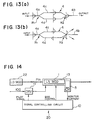
- FIGS. 13(a) and 13(b) schematically show the optical waveguide 4 of the optical waveguide device 1 of a Mach-Zehnder type.
- FIG. 13(a) shows a state of light propagation in the case where no voltage is applied
- FIG. 13(b) shows a state of light propagation in the case where a voltage is applied.
- a propagation mode is shown as a wave-like pattern in each of the waveguides (the input waveguide 4a, the output waveguide 4b and the intermediate waveguides 4c and 4d) of the optical waveguide 4.
- the direct-current light from the semiconductor laser not shown is split by the Y-shaped splitting portion R 1 when inputted to the input waveguide 4a in a predetermined input mode, inputted to the intermediate waveguides 4c and 4d, propagated in the intermediate waveguides 4c and 4d in the same mode as the input mode, recombined at the Y-shaped recombining portion R 2 , and outputted from the output waveguide 4b in the same mode.
- the direct-current light from the semiconductor laser not shown is split by the Y-shaped splitting portion R 1 when inputted to the input waveguide 4a in a predetermined input mode, then inputted to the intermediate waveguides 4c and 4d.
- a refractive index of the intermediate waveguides 4c and 4d is changed because of an applied voltage, a propagation velocity of the light is changed.
- a phase difference is generated in the lights propagated in the intermediate waveguides 4c and 4d.
- the lights having different phases are recombined at the Y-shaped recombining portion R 2 , a mode of light that should be inputted to the output waveguide 4b differs from the input mode.
- the light reaching the Y-shaped recombining portion R 2 cannot be outputted to the output waveguide 4b, and is thus radiated as radiation light to the inside of the substrate 1a.
- the signal light slightly leaks from the Y-shaped recombining portion R 2 to the inside of the substrate 1a.
- the radiation light radiated from the Y-shaped recombining portion R 2 and a part of the signal light leaking from the Y-shaped recombining portion R 2 come into the light guiding region 21 provided in the vicinity of the optical waveguide 4 (that is, in the vicinity of the both sides of the output waveguide 4b of the optical waveguide 4, in concrete).
- the light guiding region 21 guides the radiation light radiated from the Y-shaped recombining portion R 2 and the signal light leaking from the Y-shaped recombining portion R 2 such that the radiation light and the signal light are not emitted from an end surface other than an end surface on the outputting side of the substrate 1a, which functions as a light guiding unit.
- the light guiding region 21 guides light coming into the light guiding region 21 to prevent scattering of the coming light so as to increase an intensity of monitor light emitted from the end surface on the outputting side of the substrate 1a.
- An intensity of the radiation light coming into the light guiding region 21 is larger than an intensity of the signal light coming into the light guiding region 21 so that the radiation light coming thereinto is mainly guided in the light guiding region 21.
- the light guiding region 21 is formed by selectively diffusing a metal such as Ti or the like in only a part corresponding to the light guiding region portion in the substrate 1a in the titanium diffusing process when the waveguide is formed, thereby having a larger refractive index than another part (the substrate 1a), similarly to the optical waveguide 4 described before.
- a metal such as Ti or the like
- the light guiding region 21 is provided in a Position separated by about 7 to 10 ⁇ m from the output waveguide 4b of the optical waveguide 4.
- the travelling-wave electrode 2 is also formed on the output waveguide 4b (not shown in FIG. 1) in order to obtain wavelength chirp, whereby phase modulation is conducted in the output waveguide 4b in the optical modulator 20 of a Mach-Zehnder type.
- the travelling-wave electrode 2 is also formed on the light guiding region 21 (not shown in FIG. 1). However, since a voltage is also applied to the light guiding region 21 by the travelling-wave electrode 2 when the phase modulation is conducted, the refractive index of the light guiding region 21 is changed.
- a change of the refractive index of the light guiding region 21 exerts an effect on the signal light leaking from the output waveguide 4b so that the modulated waveform is degraded.
- the light guiding region 21 is provided in a position separated by about 7 to 10 ⁇ m from the output waveguide 4b.
- a shorter length of the optical waveguide 21 allows a smaller gap between the output waveguide 4b and the light guiding region 21.
- the radiation light and the signal light mentioned above coming into the light guiding region 21 interfere with each other within the light guiding region 21, then are emitted from the light guiding region 21 to the inside of the substrate 1a.
- the light (the radiation light, mainly) emitted from the light guiding region 21 further interferes with the signal light leaking from the Y-shaped recombining portion R 2 when being propagated inside the substrate 1a, then is emitted as monitor light (interference light) from the end surface on the outputting side of the substrate 1a.
- the substrate 1a in the vicinity of a portion E of the output waveguide 4b functions as an interference light generating means for making the light emitted from the light guiding region 21 and the signal light leaking from the Y-shaped recombining portion R 2 interfere with each other to generate interference light, and emitting the interference light from the end surface on the outputting side of the substrate 1a.
- a phase of the interference light emitted from the substrate 1a has an inverted phase of the signal light. Incidentally, setting of the phase of the interference light will be described later.
- the photo-detector 5 is disposed in the rear stage of the end surface on the outputting side of the substrate 1a, and the signal controlling circuit 10 is connected to a terminal T 1 of the photo-detector 5.
- a terminal T 2 of the photo-detector 5 is grounded.
- the photo-detector 5 is interposed, within the package 13, between the lens 8a arranged in the front stage of the optical fiber 9b for outputting and the end surface on the outputting side of the substrate 1a of the optical waveguide device 1 of a Mach-Zehnder type, as shown in FIG. 1.
- the photo-detector 5 is formed by placing a bear chip 6 as a photo-detecting element on a ceramic substrate 7.
- the photo-detector 5 receives the monitor light (interference light) emitted from the end surface on the outputting side of the substrate 1a, converts the received interference light into an electric signal, and outputs the electric signal to the signal controlling circuit 10, thereby monitoring the interference light.
- An example of a size of the photo-detector 5 is shown in FIG. 7.
- reference numeral 5a denotes an electrode.
- the signal controlling circuit 10 varies direct-current bias of an input electric signal to be applied to the travelling-wave electrode 2 according to a result of the monitoring by the photo-detector 5 (that is, a change of a light output electric signal from the photo-detector 5).
- an operating point of the optical modulator 20 of a Mach-Zehnder type is generally shifted with time elapsed due to temperature drift, DC drift, stress and the like.
- the photo-detector 5 monitors the interference light emitted from the end surface on the outputting side of the substrate 1a, and the signal controlling circuit 10 varies the direct-current bias of the input electric signal to be applied to the travelling-wave electrode 2 according to a result of the monitoring by the photo-detector 5, whereby the operating point of the optical modulator 20 of a Mach-Zehnder type can be controlled.
- a phase of the interference light is set such that the interference light is emitted to a position separated by a desired distance from an optical waveguide end position (an end position of the output waveguide 4b of the optical waveguide 4) on the end surface on the outputting side of the substrate 1a.
- the photo-detector 5 is disposed in a position several hundreds ⁇ m [this distance is indicated by Y in FIG. 6(b), which is about 600 to 800 ⁇ m, for example] lower than the end position of the output waveguide 4b on the end surface on the outputting side of the substrate 1a in order to prevent the signal light to be inputted to the optical fiber 9b from the output waveguide 4b from being blocked.
- the photo-detector 5 is disposed in a position separated by several hundreds ⁇ m from the end surface on the outputting side of the substrate 1a in order to further widen a radiation region of the interference light radiated from the end surface on the outputting side of the substrate 1a, as shown in FIGS. 1 and 6(a).
- FIGS. 1 and 6(a) show a case where the photo-detector 5 is disposed in a position separated by 700 ⁇ m from the end surface on the outputting side of the substrate 1a.
- a phase and an intensity of the interference light is set by adjusting a fabrication condition of the optical waveguide 4.
- the phase and the intensity of the interference light are set by varying a diffusion condition upon fabricating the optical waveguide 4 as the fabrication condition of the optical waveguide 4 so as to adjust a signal light power (signal light intensity) leaking from the Y-shaped recombining portion R 2 of the optical waveguide 4.
- the phase and the intensity of the interference light can be alternatively set by varying a length D of the output waveguide 4b of the optical waveguide 4 [that is, a length D from the Y-shaped recombining portion R 2 of the optical waveguide 4 to the end surface on the outputting side of the substrate 1a; refer to FIGS. 1 and 6(a)] as the fabrication condition of the optical waveguide 4 so as to adjust the signal light power leaking when propagated in the output waveguide 4b.
- a length of the output waveguide 4b is set to, for example, 4.5 mm or more in order to allow the interference light to be radiated on the entire of the end surface on the outputting side of the substrate 1a.
- the optical modulator 20 of a Mach-Zehnder type with the above structure when direct-current light from the semiconductor laser not shown is inputted to the package 13 through the optical fiber 9a, the incident light is inputted to the optical waveguide 4 of the optical waveguide device 1 of a Mach-Zehnder type.
- the light inputted from the input waveguide 4a is split by the Y-shaped splitting portion R 1 , modulated by the travelling-wave electrode 2 and the grounding electrode 3 while being propagated in the intermediate waveguides 4c and 4d, then the modulated lights are recombined by the Y-shaped recombining portion R 2 of the optical waveguide 4.
- signal light and radiation light are generated at the Y-shaped recombining portion R 2 , and the signal light is outputted from the output waveguide 4b, whereas the radiation light is radiated to the inside of the substrate 1a from the Y-shaped recombining portion R 2 .
- the signal light slightly leaks from the Y-shaped recombining portion R 2 to the inside of the substrate 1a.
- the radiation light and the leaking signal light come into the light guiding region 21.
- the incident light is guided by the light guiding region 21 while being prevented from being scattered, then emitted to the inside of the substrate 1a.
- the light emitted from the light guiding region 21 interferes with the signal light leaking from the Y-shaped recombining portion R 2 when propagated inside the substrate 1a, then emitted as interference light from the end surface on the outputting side of the substrate 1a.
- the phase of the interference light is set by adjusting the fabrication condition of the optical waveguide 4 at this time as stated before, the interference light is emitted to a position separated by a desired distance from the end position of the output waveguide 4b on the end surface on the outputting side of the substrate 1a.
- the emitted interference light is received by the photo-detector 5 disposed in a relevant position.
- the photo-detector 5 converts the received interference light into an electric signal, and outputs the electric signal to the signal controlling circuit 10.
- the signal controlling circuit 10 varies direct-current bias of the input electric signal to be applied to the travelling-wave electrode 2 according to a change of the light output electric signal from the photo-detector 5, thereby controlling the operating point of the optical modulator 20 of a Mach-Zehnder type.
- the signal light outputted from the output waveguide 4b of the optical waveguide device 1 of a Mach-Zehnder type is outputted via the lens 8a to the optical fiber 9b connected to the package 13.
- FIGS. 14 through 16 illustrate a characteristic of interference light intensity.
- FIGS. 23 through 25 illustrate results of BPM (Beam Profile Method) simulation.
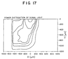
- FIGS. 17 and 20 illustrate power distribution of signal light.
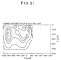
- FIG. 18 and 21 illustrate power distribution of radiation light.
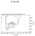
- FIGS. 19 and 22 illustrate phase distribution of interference light.
- FIGS. 17 and 18 show power distribution of the signal light and power distribution of the radiation light, respectively, in this case. From FIGS. 17 and 18, phase distribution of interference light is as shown in FIG. 19.
- a phase of the interference light has the same phase as the signal light.
- the interference light is emitted to a position about 600 to 800 ⁇ m lower than the end position of the output waveguide 4b on the end surface on the outputting side of the substrate 1a.
- FIG. 23 shows distribution of light radiated or leaking from the Y-shaped recombining portion R 2 of the optical waveguide 4.
- FIGS. 20 and 21 show power distribution of the signal light and power distribution of the radiation light, respectively, in this case. From FIGS. 20 and 21, phase distribution of the interference light is as shown in FIG. 22.
- the interference light Since an intensity of the radiation light is increased in this case, the interference light has an inverted phase of the signal light.
- the interference light is emitted to a position about 600 to 800 ⁇ m lower than the end position of the output substrate 4b on the end surface on the outputting side of the substrate 1a.
- FIGS. 24 and 25 show results of the BPM simulation in this case.
- FIGS. 24 and 25 show distribution of light radiated or leaking from the Y-shaped recombining portion R 2 of the light waveguide 4.
- widths of the light guiding region 21 are 100 ⁇ m and 200 ⁇ m, respectively.
- a width of the light guiding region 21 is increased as shown in FIG. 25, it is possible to largely decrease scattering of the light emitted from the Y-shaped recombining portion R 2 , and guide the radiation light to a wide region on the end surface on the outputting side of the substrate 1a.
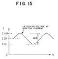
- FIG. 16 there are shown an example of an interference light intensity R D C and R A C in the case where the light guiding region 21 is provided by reference character K 2 , and an example of the interference light intensity R D C and R A C in the case where the light guiding region 21 is not provided by reference character K 1 .
- the light guiding region 21 is provided, it is possible to increase R A C as compared with a case where the light guiding region 21 is not provided, as shown in FIG. 16. It is therefore possible to improve the S/N ratio in the signal controlling circuit 10 and stabilize the operating point control in the optical modulator 20 of a Mach-Zehnder type.
- X ( ⁇ m) entered along the horizontal axis and Y ( ⁇ m) entered along the vertical axis correspond to X and Y (Y corresponds to the distance Y described before) shown in FIG. 6(b), respectively.
- the end position of the output waveguide 4b on the end surface on the outputting side of the substrate 1a is indicated by 0, a length in the rightward direction from the end position of the output waveguide 4b is indicated by a positive numeral value, whereas an a length in the leftward direction is indicated by a negative numeral value.
- power distribution of the signal light, power distribution of the radiation light, or phase distribution of the interference light is asymmetric.
- a reason of this is that the optical waveguide device 1 of a Mach-Zehnder type with the end surface on the outputting side of the substrate 1a obliquely cut when looked from the above is used in order to diminish reflected feedback light of the emitted light (refer to FIG. 1).
- the optical modulator 20 of a Mach-Zehnder type guides light radiated or leaking from the optical waveguide 4 by the light guiding region 21, besides using interference light of the light emitted from light guiding region 21 and signal light leaking from the optical waveguide 4 as monitor light used when the operating point is controlled, thereby increasing an intensity of the monitor light (interference light) emitted from the end surface on the outputting side of the substrate 1a while adjusting a position on the end surface on the outputting side of the substrate 1a to which the monitor light is emitted.
- the photo-detector 5 is disposed in a position a predetermined length (the distance Y) lower than the end position of the output waveguide 4b on the end surface on the outputting side of the substrate 1a. It is thereby possible to prevent the signal light to be outputted to the optical fiber 9b from the output waveguide 4b of the optical waveguide 4 from being blocked.
- the photo-detector 5 is disposed in a position separated by several hundreds ⁇ m (about 700 ⁇ m, for example) from the end surface on the outputting side of the substrate 1a. It is thereby possible to further widen a radiation region of the interference light emitted from the end surface on the outputting side of the substrate 1a.
- the length D of the output waveguide 4b of the optical waveguide 4 is set to, for example, 4.5 mm or more, it is possible to radiate the interference light on the entire of the end surface on the outputting side of the substrate 1a so that the interference light can be readily monitored by the photo-detector 5.
- the light guiding region 21 may have a shape as shown in FIG. 9(b) or 9(c).
- the light guiding region 21 has a shape such that a width thereof is gradually narrowed as getting closer to the end surface on the outputting side of the substrate 1a as shown in FIG. 9(c), it is possible to increase condensation of the light radiated or leaking from the optical waveguide 4.
- the light guiding region 21 is provided in the vicinity of an outputting-side waveguide with a recombining portion formed by the Y-shaped recombining portion R 2 and the output waveguide 4b of the optical waveguide 4, as shown in FIGS. 10(a) through 10(c), it is possible to further increase condensation of light radiated or leaking from the optical waveguide 4.
- This embodiment has been described by way of an example where the light guiding region 21 is provided on the both sides of the output waveguide 4b. However, it is alternatively possible to provide the light guiding region 21 on only one side of the output waveguide 4b.
- this embodiment has been described by way of an example where the light guiding region 21 is formed in the titanium diffusing process to diffuse a metal such as Ti in the substrate 1a.
- a mask pattern of the light guiding region 21 is formed on the substrate 1a [refer to FIG. 8(a)], then heat-treated with, for example, pyrophosphoric acid to conduct a proton exchanging process [refer to FIG. 8(b)], whereby the light guiding region 21 may be formed.
- a proportion of the proton exchange in the light guiding region 21 can be adjusted by an annealing process in oxygen (in O 2 ) at a high temperature of 350° C [refer to FIG. 8(c)].
- the light waveguide 4 may be formed in the proton exchanging process.
- the light guiding region 21 guides only the radiation light radiated from the optical waveguide 4.
- the output waveguide 4b is formed by a curved waveguide having a curved portion as shown in FIG. 11, light emitted from the end surface on the outputting side of the substrate 1a can be prevented from again coming into the intermediate waveguides 4c and 4d, and the like.
- FIG. 26 is a schematic view of a modified optical modulator according to the embodiment of this invention.
- the optical modulator shown in FIG. 26 is an optical modulator of a Mach-Zehnder type in a fiber direct-connect system. Similarly to the optical modulator shown in FIG. 1, the optical modulator shown in FIG. 26 is used, in a transmitting unit of, for example, an ultra high-speed optical communication system, as an external optical modulator for modulating light emitted from a signal light source such as a semiconductor laser or the like.
- FIG. 27 is a sectional view of the optical modulator 20A of a Mach-Zehnder type shown in FIG. 26 taken along line B-B.
- the optical modulator 20A of a Mach-Zehnder type shown in FIG. 26 is formed similarly to the optical modulator 20 of a Mach-Zehnder type shown in FIG. 1, excepting that the optical fibers 9a and 9b are directly connected to the optical waveguide device 1 of a Mach-Zehnder type within the package 13.
- a tip of the optical fiber 9a is fixed to an end of the input waveguide 4a on the end surface on the inputting side of the substrate 1a of the optical waveguide device 1 of a Mach-Zehnder type, whereas a tip of the optical fiber 9b is fixed to an end of the output waveguide 4b on the end surface on the outputting side of the substrate 1a of the optical waveguide device 1 of a Mach-Zehnder type, both with an adhesive C or the like.
- the photo-detector 5 is disposed in the rear stage of the end surface on the outputting side of the substrate 1a to which the optical fiber 9b is connected, below the optical fiber 9b, as shown in FIGS. 26 and 27.
- the optical modulator 20A of the Mach-Zehnder type may achieve the same functions and effects as the above-described optical modulator 20 of a Mach-Zehnder type according to the embodiment.
- the optical modulator 20A of a Mach-Zehnder type is in a fiber direct-connect system, the phase of the interference light is arbitrarily set, and optical fiber 9b and the photo-detector 5 are disposed a desired distance apart, whereby the optical modulator 20A of a Mach-Zehnder type may be readily fabricated.
- the optical modulator 20A of a Mach-Zehnder type it is possible to provide the light guiding region 21 on only one side of the output waveguide 4b, as well.
Abstract
Description

Claims (18)
- An optical modulator comprising:a substrate (1a) having electrooptic effect;an optical waveguide of a Mach-Zehnder type (4) formed on said substrate (1a);an electrode (2) formed on said substrate (1a) to control light propagated in said optical waveguide (4);a light guiding unit (21) for guiding light radiated or leaking from said optical waveguide (4); andan interference light generating means for making light emitted from said light guiding unit (21) and signal light leaking from said optical waveguide (4) interfere with each other to generate interference light, and emitting said interference light from an end surface of said substrate (1a).
- The optical modulator according to claim 1 further comprising:a photo-detector (5) for monitoring said interference light obtained by said interference light generating means; anda signal controlling circuit (10) for varying direct-current bias to be applied to said electrode (2) according to a change of said interference light monitored by said photo-detector (5) to control an operating point of said optical modulator.
- The optical modulator according to claim 1, wherein a refractive index of said light guiding unit (21) is such set as to differ from a refractive index of said substrate (1a).
- The optical modulator according to claim 1, wherein said light guiding unit (21) guides radiated light radiated from said optical waveguide (4).
- The optical modulator according to claim 1, wherein said light guiding unit (21) guides radiated light radiated from said optical waveguide (4) and the signal light leaking from said optical waveguide (4).
- The optical modulator according to claim 1, wherein said light guiding unit (21) is provided in the vicinity of an outputting-side optical waveguide (4b) forming said optical waveguide (4).
- The optical modulator according to claim 1, wherein said light guiding unit (21) is provided in the vicinity of an outputting-side optical waveguide with a recombining portion having a recombining portion (R2) forming said optical waveguide (4) and the outputting-side optical waveguide (4b) forming said optical waveguide (4) and connected to said recombining portion (R2).
- The optical modulator according to claim 1, wherein said light guiding unit (21) is formed as a light guiding unit fabricated by titanium diffusion.
- The optical modulator according to claim 1, wherein said light guiding unit (21) is formed as a light guiding unit fabricated by ion exchange.
- The optical modulator according to claim 6, wherein said outputting-side optical waveguide (4b) is a linear optical waveguide.
- The optical modulator according to claim 6, wherein said outputting-side optical waveguide (4b) is a curved optical waveguide having a curved portion.
- The optical modulator according to claim 1, wherein said interference light is such set as to have an inverted phase of said signal light.
- The optical modulator according to claim 2, wherein said photo-detector (5) is disposed between the end surface of said substrate (1a) and a lens (8a) disposed in a front stage of an optical fiber (9b) for outputting.
- The optical modulator according to claim 2, wherein said photo-detector (5) is disposed in a rear stage of the end surface of said substrate (1a) to which an optical fiber (9b) for outputting is coupled.
- The optical modulator according to claim 2, wherein said photo-detector (5) is formed by placing a photo-detecting element (6) on a plate member (7).
- The optical modulator according to claim 15, wherein said plate member (7) is a ceramic substrate.
- The optical modulator according to claim 15, wherein said photo-detecting element (6) is a bear chip.
- The optical modulator according to claim 1, wherein said substrate (1a) is a lithium niobate substrate.
Applications Claiming Priority (2)
| Application Number | Priority Date | Filing Date | Title |
|---|---|---|---|
| JP32489/97 | 1997-02-14 | ||
| JP03248997A JP3742477B2 (en) | 1997-02-17 | 1997-02-17 | Light modulator |
Publications (3)
| Publication Number | Publication Date |
|---|---|
| EP0859263A2 true EP0859263A2 (en) | 1998-08-19 |
| EP0859263A3 EP0859263A3 (en) | 1998-12-23 |
| EP0859263B1 EP0859263B1 (en) | 2010-09-08 |
Family
ID=12360413
Family Applications (1)
| Application Number | Title | Priority Date | Filing Date |
|---|---|---|---|
| EP97113223A Expired - Lifetime EP0859263B1 (en) | 1997-02-17 | 1997-07-31 | Optical modulator |
Country Status (4)
| Country | Link |
|---|---|
| US (1) | US5953466A (en) |
| EP (1) | EP0859263B1 (en) |
| JP (1) | JP3742477B2 (en) |
| DE (1) | DE69739985D1 (en) |
Cited By (3)
| Publication number | Priority date | Publication date | Assignee | Title |
|---|---|---|---|---|
| EP1315021A2 (en) | 2001-11-16 | 2003-05-28 | Ngk Insulators, Ltd. | Optical modulators and a method for modulating light |
| EP1653273A1 (en) * | 2004-06-15 | 2006-05-03 | Anritsu Corporation | Optical modulator with monitor photodetector |
| EP1816506A1 (en) * | 2006-02-02 | 2007-08-08 | Yokogawa Electric Corporation | Optical modulator for burst-mode transmission |
Families Citing this family (23)
| Publication number | Priority date | Publication date | Assignee | Title |
|---|---|---|---|---|
| US6128424A (en) * | 1998-03-31 | 2000-10-03 | Litton Systems Inc. | Dual purpose input electrode structure for MIOCs (multi-function integrated optics chips) |
| JP2002023123A (en) * | 2000-07-11 | 2002-01-23 | Fujitsu Ltd | Optical circuit provided with optical waveguide for guiding minor light |
| EP1306703A1 (en) * | 2001-10-23 | 2003-05-02 | Corning O.T.I. S.p.A. | Optical devices for communication |
| US20040028334A1 (en) * | 2002-05-06 | 2004-02-12 | Marco Marazzi | Active optical devices and methods of controlling them |
| US7009750B1 (en) | 2002-10-25 | 2006-03-07 | Eclipse Energy Systems, Inc. | Apparatus and methods for modulating refractive index |
| WO2005089332A2 (en) * | 2004-03-12 | 2005-09-29 | The Government Of The United States Of America, As Represented By The Secretary Of The Navy | Low loss electrodes for electro-optic modulators |
| US7426326B2 (en) * | 2004-03-12 | 2008-09-16 | The United States Of America As Represented By The Secretary Of The Navy | Low loss bridge electrode with rounded corners for electro-optic modulators |
| JP4911529B2 (en) | 2005-02-22 | 2012-04-04 | 日本碍子株式会社 | Light modulator |
| JP4874685B2 (en) * | 2005-03-25 | 2012-02-15 | 住友大阪セメント株式会社 | Light modulator |
| US7444039B2 (en) * | 2005-03-25 | 2008-10-28 | Sumitomo Osaka Cement Co., Ltd. | Optical modulator |
| JP4658658B2 (en) * | 2005-03-29 | 2011-03-23 | 住友大阪セメント株式会社 | Light modulator |
| US20060263097A1 (en) * | 2005-05-23 | 2006-11-23 | Fujitsu Limited | Optical transmitting apparatus, optical receiving apparatus, and optical communication system comprising them |
| JP4922594B2 (en) | 2005-05-23 | 2012-04-25 | 富士通株式会社 | Optical transmitter, optical receiver, and optical communication system including them |
| JP4657860B2 (en) | 2005-09-16 | 2011-03-23 | 富士通株式会社 | Optical transmitter and optical communication system |
| JP2007093717A (en) * | 2005-09-27 | 2007-04-12 | Oki Electric Ind Co Ltd | Optical modulator and control method thereof |
| US7764851B2 (en) | 2007-11-01 | 2010-07-27 | Ngk Insulators, Ltd. | Optical modulators |
| US7783138B2 (en) * | 2007-11-16 | 2010-08-24 | Jds Uniphase Corporation | Free-space integrated photodetector with reduced phase tracking error |
| JP2011164388A (en) * | 2010-02-10 | 2011-08-25 | Fujitsu Optical Components Ltd | Mach-zehnder optical modulator |
| JP5108042B2 (en) * | 2010-03-11 | 2012-12-26 | 日本電信電話株式会社 | Light modulator |
| WO2012165656A1 (en) | 2011-06-01 | 2012-12-06 | 日本電気株式会社 | Optical waveguide device, optical interferometer, and method for producing optical waveguide device |
| JP5660095B2 (en) * | 2012-08-31 | 2015-01-28 | 住友大阪セメント株式会社 | Light modulator |
| US20170235047A1 (en) * | 2014-08-04 | 2017-08-17 | Sumitomo Bakelite Co., Ltd. | Waveguide |
| CN111308740A (en) * | 2020-03-10 | 2020-06-19 | 苏州康冠光电科技有限公司 | High extinction ratio electro-optical intensity modulator |
Citations (1)
| Publication number | Priority date | Publication date | Assignee | Title |
|---|---|---|---|---|
| JPH0553086A (en) | 1991-08-28 | 1993-03-05 | Fujitsu Ltd | Mach-zhender type optical waveguide device |
Family Cites Families (8)
| Publication number | Priority date | Publication date | Assignee | Title |
|---|---|---|---|---|
| GB8822288D0 (en) * | 1988-09-22 | 1988-10-26 | Bt & D Technologies Ltd | Electro-optic device |
| JP2738078B2 (en) * | 1989-11-01 | 1998-04-08 | 富士通株式会社 | Light modulator |
| JP2642499B2 (en) * | 1990-03-01 | 1997-08-20 | 富士通株式会社 | Optical transmitter, optical modulator control circuit, and optical modulation method |
| JP2800368B2 (en) * | 1990-05-18 | 1998-09-21 | 富士通株式会社 | Light modulator |
| US5199086A (en) * | 1991-01-17 | 1993-03-30 | Massachusetts Institute Of Technology | Electro-optic system |
| US5267336A (en) * | 1992-05-04 | 1993-11-30 | Srico, Inc. | Electro-optical sensor for detecting electric fields |
| WO1994028455A1 (en) * | 1993-06-01 | 1994-12-08 | United Technologies Corporation | An electro-optic modulator having gated-dither bias control |
| JPH08194195A (en) * | 1995-01-20 | 1996-07-30 | Hoya Corp | Optical waveguide element |
-
1997
- 1997-02-17 JP JP03248997A patent/JP3742477B2/en not_active Expired - Lifetime
- 1997-07-28 US US08/901,336 patent/US5953466A/en not_active Expired - Lifetime
- 1997-07-31 DE DE69739985T patent/DE69739985D1/en not_active Expired - Lifetime
- 1997-07-31 EP EP97113223A patent/EP0859263B1/en not_active Expired - Lifetime
Patent Citations (1)
| Publication number | Priority date | Publication date | Assignee | Title |
|---|---|---|---|---|
| JPH0553086A (en) | 1991-08-28 | 1993-03-05 | Fujitsu Ltd | Mach-zhender type optical waveguide device |
Cited By (8)
| Publication number | Priority date | Publication date | Assignee | Title |
|---|---|---|---|---|
| EP1315021A2 (en) | 2001-11-16 | 2003-05-28 | Ngk Insulators, Ltd. | Optical modulators and a method for modulating light |
| EP1315021A3 (en) * | 2001-11-16 | 2004-01-28 | Ngk Insulators, Ltd. | Optical modulators and a method for modulating light |
| US6904186B2 (en) | 2001-11-16 | 2005-06-07 | Ngk Insulators, Ltd. | Optical modulators and a method for modulating light |
| EP1653273A1 (en) * | 2004-06-15 | 2006-05-03 | Anritsu Corporation | Optical modulator with monitor photodetector |
| EP1653273A4 (en) * | 2004-06-15 | 2007-12-19 | Anritsu Corp | Optical modulator with monitor photodetector |
| US7474812B2 (en) | 2004-06-15 | 2009-01-06 | Anritsu Corporation | Monitor photodetector equipped optical modulator |
| EP1816506A1 (en) * | 2006-02-02 | 2007-08-08 | Yokogawa Electric Corporation | Optical modulator for burst-mode transmission |
| US7672033B2 (en) | 2006-02-02 | 2010-03-02 | Yokogawa Electric Corporation | Light modulating apparatus |
Also Published As
| Publication number | Publication date |
|---|---|
| EP0859263A3 (en) | 1998-12-23 |
| EP0859263B1 (en) | 2010-09-08 |
| JP3742477B2 (en) | 2006-02-01 |
| US5953466A (en) | 1999-09-14 |
| JPH10228006A (en) | 1998-08-25 |
| DE69739985D1 (en) | 2010-10-21 |
Similar Documents
| Publication | Publication Date | Title |
|---|---|---|
| EP0859263B1 (en) | Optical modulator | |
| US5991471A (en) | Configurable chirp mach-zehnder optical modulator | |
| US5963357A (en) | Optical modulator | |
| US8149492B2 (en) | Optical modulator | |
| EP0809129B1 (en) | Semiconductor optical modulator and method for making the same | |
| US7911675B2 (en) | Optical modulation device and optical semiconductor device | |
| EP0562695A1 (en) | Controllable polarisation transformer | |
| WO2004068221A1 (en) | Optical modulator | |
| JPH0921986A (en) | Semiconductor phase modulator and modulation method of lightsignal | |
| JP2800368B2 (en) | Light modulator | |
| JP2738078B2 (en) | Light modulator | |
| US7474812B2 (en) | Monitor photodetector equipped optical modulator | |
| JPH07318986A (en) | Waveguide type optical switch | |
| JPH05134220A (en) | Optical transmitter | |
| JPH07106691A (en) | Integrated light source with external modulator and driving method therefor | |
| JPH1184434A (en) | Light control circuit and its operation method | |
| US7373025B2 (en) | Waveguide-type optical device | |
| WO2002056098A1 (en) | Optical monitoring in optical interferometric modulators | |
| JP3717639B2 (en) | Optical modulator module | |
| JPH02165117A (en) | Operation stabilizing method for waveguide type optical modulator | |
| JP2005316041A (en) | Optical modulator | |
| JPH0373916A (en) | Driving system for optical modulator | |
| JPH06130337A (en) | Analog modulator | |
| JPS61156209A (en) | Module of light controlling element |
Legal Events
| Date | Code | Title | Description |
|---|---|---|---|
| PUAI | Public reference made under article 153(3) epc to a published international application that has entered the european phase |
Free format text: ORIGINAL CODE: 0009012 |
|
| AK | Designated contracting states |
Kind code of ref document: A2 Designated state(s): DE FR GB IT |
|
| PUAL | Search report despatched |
Free format text: ORIGINAL CODE: 0009013 |
|
| AK | Designated contracting states |
Kind code of ref document: A3 Designated state(s): AT BE CH DE DK ES FI FR GB GR IE IT LI LU MC NL PT SE |
|
| 17P | Request for examination filed |
Effective date: 19981223 |
|
| AKX | Designation fees paid |
Free format text: DE FR GB IT |
|
| 17Q | First examination report despatched |
Effective date: 20050628 |
|
| GRAJ | Information related to disapproval of communication of intention to grant by the applicant or resumption of examination proceedings by the epo deleted |
Free format text: ORIGINAL CODE: EPIDOSDIGR1 |
|
| GRAP | Despatch of communication of intention to grant a patent |
Free format text: ORIGINAL CODE: EPIDOSNIGR1 |
|
| RIN1 | Information on inventor provided before grant (corrected) |
Inventor name: ITOH, TOMOYUKI Inventor name: OTANI, TOSHIHIRO Inventor name: OMORI, YASUHIRO Inventor name: KUBOTA, YOSHINOBU |
|
| GRAS | Grant fee paid |
Free format text: ORIGINAL CODE: EPIDOSNIGR3 |
|
| GRAA | (expected) grant |
Free format text: ORIGINAL CODE: 0009210 |
|
| STAA | Information on the status of an ep patent application or granted ep patent |
Free format text: STATUS: THE PATENT HAS BEEN GRANTED |
|
| AK | Designated contracting states |
Kind code of ref document: B1 Designated state(s): DE FR GB IT |
|
| REG | Reference to a national code |
Ref country code: GB Ref legal event code: FG4D |
|
| REF | Corresponds to: |
Ref document number: 69739985 Country of ref document: DE Date of ref document: 20101021 Kind code of ref document: P |
|
| PLBE | No opposition filed within time limit |
Free format text: ORIGINAL CODE: 0009261 |
|
| 26N | No opposition filed |
Effective date: 20110609 |
|
| REG | Reference to a national code |
Ref country code: DE Ref legal event code: R097 Ref document number: 69739985 Country of ref document: DE Effective date: 20110609 |
|
| REG | Reference to a national code |
Ref country code: FR Ref legal event code: PLFP Year of fee payment: 19 |
|
| PGFP | Annual fee paid to national office [announced via postgrant information from national office to epo] |
Ref country code: DE Payment date: 20150729 Year of fee payment: 19 Ref country code: GB Payment date: 20150729 Year of fee payment: 19 |
|
| PGFP | Annual fee paid to national office [announced via postgrant information from national office to epo] |
Ref country code: FR Payment date: 20150629 Year of fee payment: 19 |
|
| PGFP | Annual fee paid to national office [announced via postgrant information from national office to epo] |
Ref country code: IT Payment date: 20150727 Year of fee payment: 19 |
|
| REG | Reference to a national code |
Ref country code: DE Ref legal event code: R119 Ref document number: 69739985 Country of ref document: DE |
|
| GBPC | Gb: european patent ceased through non-payment of renewal fee |
Effective date: 20160731 |
|
| PG25 | Lapsed in a contracting state [announced via postgrant information from national office to epo] |
Ref country code: DE Free format text: LAPSE BECAUSE OF NON-PAYMENT OF DUE FEES Effective date: 20170201 Ref country code: FR Free format text: LAPSE BECAUSE OF NON-PAYMENT OF DUE FEES Effective date: 20160801 |
|
| REG | Reference to a national code |
Ref country code: FR Ref legal event code: ST Effective date: 20170331 |
|
| PG25 | Lapsed in a contracting state [announced via postgrant information from national office to epo] |
Ref country code: GB Free format text: LAPSE BECAUSE OF NON-PAYMENT OF DUE FEES Effective date: 20160731 |
|
| PG25 | Lapsed in a contracting state [announced via postgrant information from national office to epo] |
Ref country code: IT Free format text: LAPSE BECAUSE OF NON-PAYMENT OF DUE FEES Effective date: 20160731 |