EP0859399A2 - Semiconductor wafer polishing apparatus with a flexible carrier plate - Google Patents
Semiconductor wafer polishing apparatus with a flexible carrier plate Download PDFInfo
- Publication number
- EP0859399A2 EP0859399A2 EP98301043A EP98301043A EP0859399A2 EP 0859399 A2 EP0859399 A2 EP 0859399A2 EP 98301043 A EP98301043 A EP 98301043A EP 98301043 A EP98301043 A EP 98301043A EP 0859399 A2 EP0859399 A2 EP 0859399A2
- Authority
- EP
- European Patent Office
- Prior art keywords
- wafer
- carrier
- rigid plate
- carrier head
- recited
- Prior art date
- Legal status (The legal status is an assumption and is not a legal conclusion. Google has not performed a legal analysis and makes no representation as to the accuracy of the status listed.)
- Withdrawn
Links
Images

Classifications
-
- H—ELECTRICITY
- H01—ELECTRIC ELEMENTS
- H01L—SEMICONDUCTOR DEVICES NOT COVERED BY CLASS H10
- H01L21/00—Processes or apparatus adapted for the manufacture or treatment of semiconductor or solid state devices or of parts thereof
- H01L21/02—Manufacture or treatment of semiconductor devices or of parts thereof
- H01L21/04—Manufacture or treatment of semiconductor devices or of parts thereof the devices having at least one potential-jump barrier or surface barrier, e.g. PN junction, depletion layer or carrier concentration layer
- H01L21/18—Manufacture or treatment of semiconductor devices or of parts thereof the devices having at least one potential-jump barrier or surface barrier, e.g. PN junction, depletion layer or carrier concentration layer the devices having semiconductor bodies comprising elements of Group IV of the Periodic System or AIIIBV compounds with or without impurities, e.g. doping materials
- H01L21/30—Treatment of semiconductor bodies using processes or apparatus not provided for in groups H01L21/20 - H01L21/26
- H01L21/302—Treatment of semiconductor bodies using processes or apparatus not provided for in groups H01L21/20 - H01L21/26 to change their surface-physical characteristics or shape, e.g. etching, polishing, cutting
- H01L21/304—Mechanical treatment, e.g. grinding, polishing, cutting
-
- B—PERFORMING OPERATIONS; TRANSPORTING
- B24—GRINDING; POLISHING
- B24B—MACHINES, DEVICES, OR PROCESSES FOR GRINDING OR POLISHING; DRESSING OR CONDITIONING OF ABRADING SURFACES; FEEDING OF GRINDING, POLISHING, OR LAPPING AGENTS
- B24B37/00—Lapping machines or devices; Accessories
- B24B37/27—Work carriers
- B24B37/30—Work carriers for single side lapping of plane surfaces
- B24B37/32—Retaining rings
Definitions
- the present invention relates to semiconductor processing equipment, and more particularly to carriers for holding a semiconductor wafer during polishing.
- Semiconductor wafers are polished to achieve a smooth, flat finish before performing process steps that create electrical circuits on the wafer. This polishing is accomplished by securing the wafer to a carrier, rotating the carrier and placing a rotating polishing pad in contact with the rotating wafer.
- a common type of carrier is securely attached to a shaft which is rotated by a motor.
- a wet polishing slurry usually comprising a polishing abrasive suspended in a liquid, was applied to the polishing pad.
- a downward polishing pressure was applied between the rotating wafer and the rotating polishing pad during the polishing operation. This system required that the wafer carrier and polishing pad be aligned perfectly parallel in order to properly polish the semiconductor wafer surface.
- the wafer carrier typically was a hard, flat plate which did not conform to the surface of the wafer which opposite to the surface being polished. As a consequence, the carrier plate was not capable of applying a uniform polish pressure across the entire area of the wafer, especially at the edge of the wafer. In an attempt to overcome this problem, the hard carrier plate often was covered by a softer carrier film. The purpose of the film was to transmit uniform pressure to the back surface of the wafer to aid in uniform polishing. In addition to compensating for surface irregularities between the carrier plate and the back wafer surface, the film also was supposed to smooth over minor contaminants on the wafer surface. Such contaminants could produce to high pressure areas in the absence of such a carrier film. Unfortunately, the films were only partially effective with limited flexibility and tended to take a "set" after repeated usage. In particular, the set appeared to be worse at the edges of the semiconductor wafer.
- a general object of the present invention is to provide an improved wafer carrier mechanism for polishing semiconductor wafers.
- Another object is to provide a carrier which applies uniform pressure over the entire area of the semiconductor wafer.
- a further object of the present invention is to provide a surface on the carrier which contacts the back surface of the semiconductor wafer and conforms to any irregularities of that back surface.
- the surface of the carrier plate should conform to even minute irregularities in the back surface of the semiconductor wafer.
- Yet another object is to provide a carrier plate which eliminates the greater erosion adjacent the semiconductor wafer edge as produced by previous carriers.
- a carrier head for a semiconductor wafer polishing apparatus, which includes a rigid plate having a major surface.
- a wafer carrier membrane of soft, flexible material has a wafer contact section for contacting the semiconductor wafer.
- the wafer carrier membrane is connected to the rigid plate and extends across at least a portion of the major surface defining a cavity therebetween.
- a retaining ring is secured to the rigid plate around the wafer contact section of the wafer carrier membrane.
- a fluid conduit enables sources of vacuum and pressurized fluid to be connected alternately to the cavity.
- the major surface of the plate has a plurality of open channels which aid the flow of fluid between the plate and the wafer carrier membrane.
- the major surface may have a plurality of concentric annular channels interconnected by a plurality of radially extending channels.
- the preferred embodiment of the wafer carrier membrane has the wafer contact section surrounded by a bellows from which a flange outwardly extends.
- the flange is sandwiched between the major surface and the retaining ring to form the cavity.
- the cavity is pressurized with fluid which causes the membrane to exert force against the semiconductor wafer pushing the wafer into an adjacent polishing pad.
- the wafer carrier membrane is very thin, soft and highly flexible, it conforms to the back surface of the semiconductor wafer which is opposite to the surface to be polished. By conforming even minute variations in the wafer surface, the membrane and exerts pressure evenly over the entire back surface of the semiconductor wafer thereby producing uniform polishing.
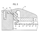
- a semiconductor wafer polishing apparatus has a carrier head 10 mounted on a spindle shaft 12 that is connected to a rotational drive mechanism by a gimbal assembly (not shown).
- the end of the spindle shaft 12 is fixedly attached to a rigid carrier plate 14 with a flexible sealing ring 16 therebetween to prevent fluid from leaking between the spindle shaft and the carrier plate.
- the carrier plate 14 has a planar upper surface 18 and a parallel lower surface 20.
- the lower surface 20 of the carrier plate 14 has a plurality of grooves therein as shown in Figure 2.
- the lower surface 20 has a central recessed area 22 with three spaced apart concentric annular grooves 23, 24 and 25 in order of increasing diameter.
- An annular recess 26 extends around the peripheral edge of the lower surface 20.
- Four axial grooves 31, 32, 33 and 34 extend at ninety degree intervals from the central recess 22 to the peripheral recess 26 through each of the annular grooves 23-25.
- each of the annular grooves, central recess, and peripheral recess communicate with each other through the axial grooves 31-34.
- apertures 36 extend from the central recess 22 through the carrier plate 14 to a recess on the upper surface 18 in which the spindle shaft 12 is received, as seen in Figure 1.
- Apertures 36 communicate with apertures 38 through the end of the spindle shaft 12 thereby providing a passage from a central bore 39 of the spindle shaft 12 to the underside of the carrier plate 14.
- a retaining ring 40 is attached to the lower surface 20 of the carrier plate 14 at the peripheral recess 26.
- the retaining ring 40 is secured by a plurality of cap screws 42 which are received within apertures 44 that open into the peripheral recess 26 of the carrier plate 14.
- a circular wafer carrier membrane 46 is held between the carrier plate 14 and the retaining ring 40 stretching across the lower surface 20 of the carrier plate to form a flexible diaphragm beneath the carrier plate.
- the wafer carrier membrane 46 preferably is formed of molded polyurethane, although a thin sheet of any of several soft, resilient materials may be utilized.
- the flexible wafer carrier membrane 46 has a relatively planar, circular wafer contact section 48 with a plurality of apertures 50 extending therethrough.
- the central wafer contact section 48 is between 0.5 and 3.0 millimeters thick, for example 1.0 millimeter thick.
- the central wafer contact section 48 is bounded by an annular rim 52 which has a bellows portion 54 to allow variation in the spacing between the bottom surface 20 of the carrier plate 14 and the wafer contact section 48 of the membrane 46.
- the opposite edge of the rim 52 from the wafer contact section 48 has an outwardly extending flange 56 which is squeezed between the peripheral recess surface of the carrier plate 14 and the retaining ring 40 due to the force exerted by the cap screws 42.
- the carrier head 10 In order to process a semiconductor wafer, the carrier head 10 is moved over a wafer storage area and lowered onto a semiconductor wafer 60.
- the spindle shaft 12 is connected to a vacuum source by a rotational coupling and valve (not shown). With the carrier head positioned over the semiconductor wafer 60, the vacuum valve is open which evacuates the cavity 58 formed between the carrier plate 14 and the wafer carrier membrane 46. This action draws air into this cavity 58 through the small holes 50 in the wafer carrier membrane 46 and creates suction which draws the semiconductor wafer 60 against the wafer carrier membrane.
- the interior diameter of the retaining ring 40 is less than five millimeters (preferably less than one to two millimeters) larger than the outer diameter of the semiconductor wafer 60.
- the carrier head 10 and grabbed wafer 60 then are moved over a conventional semiconductor wafer polishing pad 62 which is mounted on a standard rotating platen 64, as shown in Figure 1.
- the carrier head 10 then is lowered so that the wafer 60 contacts the surface of the polishing pad 62.
- the valve for the vacuum source is closed and a pressurized fluid is introduced into the bore 39 of the spindle shaft 12.
- this fluid preferably is a gas, such as dry air or nitrogen which will not react with the surface of the semiconductor wafer 60, liquids such as deionized water may be utilized.
- the fluid flows from the bore 39 through spindle shaft apertures 38 apertures 36 in the carrier plate 14 into the pattern of grooves 23-34 in the bottom surface 20 of the carrier plate 14 thereby filling the cavity 58 between the carrier plate and the flexible wafer carrier membrane 46.
- This action inflates the cavity 58 expanding the bellows 54 of the wafer carrier membrane 46 and exerts pressure against the semiconductor wafer 60.
- the fluid may be pressurized to less than 15 psi (preferably between 0.5 psi and 10 psi) with the precise pressure depending upon the characteristics of the semiconductor wafer 60 and the abrasive material applied to the polishing pad 62.
- the pressure from the fluid is evenly distributed throughout the cavity 54 exerting an even downward force onto the semiconductor wafer 60.
- the membrane is very thin, it conforms to the top surface of the semiconductor wafer 60.
- the membrane 46 is soft and highly flexible conforming to even the minute variations in the wafer surface. As a consequence, a carrier film is not required between the wafer and the membrane as the membrane will conform to even minor surface contaminants on the back side of the semiconductor wafer 60.
- the carrier head 10 is mechanically pressed downward so that the retaining ring 40 depresses the polishing pad 62.
- the lower edge 65 of the retaining ring 40 which contacts the polishing pad is substantially co-planar with the semiconductor wafer surface being polished.
- This co-planar relationship and the very small ( ⁇ 5 mm) difference between the inner diameter of the retaining ring 40 and the outer diameter of the semiconductor wafer 60 significantly minimizes the edge abrasive effect encountered with prior polishing techniques.
- This abrasive effect was due to depression of the polishing pad by the edge of the semiconductor wafer as it rotated against the pad.
- the retaining ring 40 of the present carrier assembly depresses the polishing pad and because only a very small gap exists between the interior surface of the retaining ring 40 and the edge of the semiconductor wafer 60, the polishing pad does not expand appreciably in that gap thereby eliminating the sever edge abrasive effect previously encountered.
- the present air pillow wafer carrier head 10 applies extremely uniform polish pressure across the entire are of the semiconductor wafer, especially at the edge of the wafer.
- the extreme flexibility and softness of the wafer carrier membrane 46 with the integral bellows 54 allows the carrier membrane 46 to respond to small disturbances on the face of the semiconductor wafer 60 which may be caused by some aspect of the polishing process such as pad variation, conditioning of the pad, and slurry flow rates.
- the flexible wafer carrier membrane is thus able to automatically compensate for such variations and provide uniform pressure between the semiconductor wafer 60 and the polishing pad 62. Any energy associated with these disturbances is absorbed by the fluid in the cavity 58 behind the wafer carrier membrane 46 instead of increasing the local polishing rate of the semiconductor wafer.
Abstract
Description
Claims (20)
- A carrier head for an apparatus which polishes a surface of a semiconductor wafer, wherein the carrier head comprises:a rigid plate having a major surface;a wafer carrier membrane of soft, flexible material with a wafer contact section for contacting the semiconductor wafer, the wafer carrier membrane connected to the rigid plate and extending across at least a portion of the major surface thereby defining a cavity therebetween;a retaining ring secured to the rigid plate around the wafer contact section of the wafer carrier membrane; anda fluid conduit by which a source of a vacuum and a source of pressurized fluid are alternately connected to the cavity.
- The carrier head as recited in claim 1 wherein the wafer carrier membrane has a plurality of apertures through the wafer contact section.
- The carrier head as recited in claim 1 wherein the wafer carrier membrane in the wafer contact section has a thickness between 0.5 and 3.0 millimeters, inclusive.
- The carrier head as recited in claim 1 wherein the wafer contact section of the wafer carrier membrane is surrounded by a bellows which is coupled to the rigid plate.
- The carrier head as recited in claim 4 wherein the wafer carrier membrane further comprises a flange extending around the bellows and abutting the rigid plate.
- The carrier head as recited in claim 1 wherein the wafer carrier membrane further includes an annular bellows having with a first end attached to the wafer contact section and having a second end, and a flange projecting from the second end and sandwiched between the major surface and the retaining ring.
- The carrier head as recited in claim 1 wherein the rigid plate has a plurality of channels on the major surface and the fluid conduit communicates with the plurality of channels.
- The carrier head as recited in claim 1 wherein the rigid plate has a plurality of concentric annular channels on the major surface.
- The carrier head as recited in claim 8 wherein the rigid plate further includes a cross channel interconnecting the plurality of concentric annular channels.
- The carrier head as recited in claim 8 wherein the rigid plate further comprises a plurality of radially extending channels on the major surface interconnecting the plurality of concentric annular channels.
- The carrier head as recited in claim 1 wherein the semiconductor wafer has a first diameter; and the retaining ring has an inner diameter which is less than five millimeters larger that the first diameter.
- The carrier head as recited in claim 1 wherein the semiconductor wafer has a first diameter; and the retaining ring has an inner diameter which is less than two millimeters larger that the first diameter.
- The carrier head as recited in claim 1 wherein the retaining ring has a surface which is substantially coplanar with the surface of the semiconductor wafer.
- The carrier head as recited in claim 1 further comprising a fluid within the cavity, wherein the fluid is selected from the group consisting of air, nitrogen and water.
- The carrier head as recited in claim 1 further comprising a fluid within the cavity, wherein the fluid has a pressure that is less than 15 psi.
- A carrier head for an apparatus which polishes a semiconductor wafer, wherein the carrier head comprises:a rigid plate having a major surface with a plurality of channels on the major surface;a wafer carrier membrane of flexible material with a wafer contact section for contacting the semiconductor wafer and having a plurality of apertures therethrough;a retaining ring secured to the rigid plate with a portion of the wafer carrier membrane sandwiched between the major surface and the retaining ring thereby defining a cavity between the wafer carrier membrane and the rigid plate; anda fluid conduit coupled to the plate by which sources of vacuum and pressurized fluid are alternately connected to the plurality of channels.
- The carrier head as recited in claim 16 wherein the plurality of channels on the rigid plate comprises a plurality of concentric annular channels and a plurality of cross channels interconnecting the plurality of concentric annular channels.
- A carrier head for an apparatus which polishes a semiconductor wafer, wherein the carrier head comprises:a rigid plate having a major surface;a wafer carrier membrane of flexible material having a wafer contact section for contacting the semiconductor wafer and having a plurality of apertures therethrough, and having an annular bellows projecting from wafer contact section and abutting the rigid plate;a retaining ring connected to the rigid plate and the annular bellows thereby defining a cavity between the wafer carrier membrane and the rigid plate; anda fluid conduit through which a source of a vacuum and source of a pressurized fluid are alternately connected to the cavity.
- The carrier head as recited in claim 18 wherein the annular bellows of the wafer carrier membrane has a flange extending therefrom and sandwiched between the major surface and the retaining ring.
- The carrier head as recited in claim 18 wherein the rigid plate has a plurality of channels on the major surface.
Applications Claiming Priority (2)
| Application Number | Priority Date | Filing Date | Title |
|---|---|---|---|
| US800941 | 1985-11-22 | ||
| US08/800,941 US5851140A (en) | 1997-02-13 | 1997-02-13 | Semiconductor wafer polishing apparatus with a flexible carrier plate |
Publications (2)
| Publication Number | Publication Date |
|---|---|
| EP0859399A2 true EP0859399A2 (en) | 1998-08-19 |
| EP0859399A3 EP0859399A3 (en) | 1999-03-24 |
Family
ID=25179777
Family Applications (1)
| Application Number | Title | Priority Date | Filing Date |
|---|---|---|---|
| EP98301043A Withdrawn EP0859399A3 (en) | 1997-02-13 | 1998-02-12 | Semiconductor wafer polishing apparatus with a flexible carrier plate |
Country Status (5)
| Country | Link |
|---|---|
| US (1) | US5851140A (en) |
| EP (1) | EP0859399A3 (en) |
| JP (1) | JP3937368B2 (en) |
| KR (1) | KR19980071275A (en) |
| IL (1) | IL123235A (en) |
Cited By (13)
| Publication number | Priority date | Publication date | Assignee | Title |
|---|---|---|---|---|
| EP0988931A2 (en) * | 1998-09-08 | 2000-03-29 | Speedfam Co., Ltd. | Carrier and polishing apparatus |
| WO2000021714A1 (en) * | 1998-10-09 | 2000-04-20 | Applied Materials, Inc. | A carrier head with a flexible membrane for chemical mechanical polishing |
| WO2000021715A2 (en) * | 1998-10-09 | 2000-04-20 | Speedfam-Ipec Corporation | Semiconductor wafer polishing apparatus with a variable polishing force wafer carrier head |
| EP1048406A2 (en) * | 1999-04-22 | 2000-11-02 | Applied Materials, Inc. | A carrier head for chemical mechanical polishing a substrate |
| EP1048408A2 (en) * | 1999-04-22 | 2000-11-02 | Applied Materials, Inc. | Carrier head with a compressible film |
| WO2002059947A2 (en) * | 2001-01-11 | 2002-08-01 | Nutool, Inc. | Carrier head for holding a wafer and allowing processing on a front face thereof to occur |
| WO2003032374A2 (en) * | 2001-10-11 | 2003-04-17 | Speedfam-Ipec Corporation | Workpiece carrier with adjustable pressure zones and barriers |
| GB2402263A (en) * | 2000-03-31 | 2004-12-01 | Speedfam Ipec Corp | Carrier including a multi-volume diaphragm for polishing a semiconductot wafer and a method therefor |
| US7635292B2 (en) | 2004-12-10 | 2009-12-22 | Ebara Corporation | Substrate holding device and polishing apparatus |
| US7867063B2 (en) | 2003-02-10 | 2011-01-11 | Ebara Corporation | Substrate holding apparatus and polishing apparatus |
| US20140370787A1 (en) * | 2012-10-29 | 2014-12-18 | Wayne O. Duescher | Vacuum-grooved membrane abrasive polishing wafer workholder |
| CN104385112A (en) * | 2014-11-04 | 2015-03-04 | 无锡市华明化工有限公司 | Grinder |
| CN104942704A (en) * | 2014-03-27 | 2015-09-30 | 株式会社荏原制作所 | Elastic membrane, substrate holding apparatus, and polishing apparatus |
Families Citing this family (118)
| Publication number | Priority date | Publication date | Assignee | Title |
|---|---|---|---|---|
| US6146259A (en) | 1996-11-08 | 2000-11-14 | Applied Materials, Inc. | Carrier head with local pressure control for a chemical mechanical polishing apparatus |
| US6183354B1 (en) | 1996-11-08 | 2001-02-06 | Applied Materials, Inc. | Carrier head with a flexible membrane for a chemical mechanical polishing system |
| JP3705670B2 (en) * | 1997-02-19 | 2005-10-12 | 株式会社荏原製作所 | Polishing apparatus and method |
| US5957751A (en) * | 1997-05-23 | 1999-09-28 | Applied Materials, Inc. | Carrier head with a substrate detection mechanism for a chemical mechanical polishing system |
| US6398621B1 (en) | 1997-05-23 | 2002-06-04 | Applied Materials, Inc. | Carrier head with a substrate sensor |
| US6001001A (en) * | 1997-06-10 | 1999-12-14 | Texas Instruments Incorporated | Apparatus and method for chemical mechanical polishing of a wafer |
| US5964653A (en) * | 1997-07-11 | 1999-10-12 | Applied Materials, Inc. | Carrier head with a flexible membrane for a chemical mechanical polishing system |
| JPH11138429A (en) * | 1997-11-11 | 1999-05-25 | Sony Corp | Polishing device |
| JP3077652B2 (en) * | 1997-11-20 | 2000-08-14 | 日本電気株式会社 | Wafer polishing method and apparatus |
| JPH11179651A (en) * | 1997-12-17 | 1999-07-06 | Ebara Corp | Substrate holder and polishing device provided with this substrate holder |
| US5993302A (en) * | 1997-12-31 | 1999-11-30 | Applied Materials, Inc. | Carrier head with a removable retaining ring for a chemical mechanical polishing apparatus |
| US6080050A (en) * | 1997-12-31 | 2000-06-27 | Applied Materials, Inc. | Carrier head including a flexible membrane and a compliant backing member for a chemical mechanical polishing apparatus |
| US6531397B1 (en) | 1998-01-09 | 2003-03-11 | Lsi Logic Corporation | Method and apparatus for using across wafer back pressure differentials to influence the performance of chemical mechanical polishing |
| JPH11285966A (en) * | 1998-04-02 | 1999-10-19 | Speedfam-Ipec Co Ltd | Carrier and cmp device |
| FR2778129B1 (en) * | 1998-05-04 | 2000-07-21 | St Microelectronics Sa | MEMBRANE SUPPORT DISC OF A POLISHING MACHINE AND METHOD OF OPERATING SUCH A MACHINE |
| US6251215B1 (en) | 1998-06-03 | 2001-06-26 | Applied Materials, Inc. | Carrier head with a multilayer retaining ring for chemical mechanical polishing |
| US5993293A (en) * | 1998-06-17 | 1999-11-30 | Speedram Corporation | Method and apparatus for improved semiconductor wafer polishing |
| US6159079A (en) * | 1998-09-08 | 2000-12-12 | Applied Materials, Inc. | Carrier head for chemical mechanical polishing a substrate |
| US6132298A (en) | 1998-11-25 | 2000-10-17 | Applied Materials, Inc. | Carrier head with edge control for chemical mechanical polishing |
| US6244942B1 (en) * | 1998-10-09 | 2001-06-12 | Applied Materials, Inc. | Carrier head with a flexible membrane and adjustable edge pressure |
| US6165058A (en) * | 1998-12-09 | 2000-12-26 | Applied Materials, Inc. | Carrier head for chemical mechanical polishing |
| US6422927B1 (en) | 1998-12-30 | 2002-07-23 | Applied Materials, Inc. | Carrier head with controllable pressure and loading area for chemical mechanical polishing |
| US6162116A (en) * | 1999-01-23 | 2000-12-19 | Applied Materials, Inc. | Carrier head for chemical mechanical polishing |
| US6368189B1 (en) * | 1999-03-03 | 2002-04-09 | Mitsubishi Materials Corporation | Apparatus and method for chemical-mechanical polishing (CMP) head having direct pneumatic wafer polishing pressure |
| US6527624B1 (en) | 1999-03-26 | 2003-03-04 | Applied Materials, Inc. | Carrier head for providing a polishing slurry |
| JP3085948B1 (en) | 1999-05-10 | 2000-09-11 | 株式会社東京精密 | Wafer polishing equipment |
| US6855043B1 (en) | 1999-07-09 | 2005-02-15 | Applied Materials, Inc. | Carrier head with a modified flexible membrane |
| US6241593B1 (en) * | 1999-07-09 | 2001-06-05 | Applied Materials, Inc. | Carrier head with pressurizable bladder |
| US6358121B1 (en) | 1999-07-09 | 2002-03-19 | Applied Materials, Inc. | Carrier head with a flexible membrane and an edge load ring |
| US6494774B1 (en) | 1999-07-09 | 2002-12-17 | Applied Materials, Inc. | Carrier head with pressure transfer mechanism |
| JP3270428B2 (en) * | 1999-07-28 | 2002-04-02 | 東芝機械株式会社 | Swivel for electric injection molding machine |
| US6206768B1 (en) | 1999-07-29 | 2001-03-27 | Chartered Semiconductor Manufacturing, Ltd. | Adjustable and extended guide rings |
| US6203408B1 (en) | 1999-08-26 | 2001-03-20 | Chartered Semiconductor Manufacturing Ltd. | Variable pressure plate CMP carrier |
| US6179694B1 (en) * | 1999-09-13 | 2001-01-30 | Chartered Semiconductor Manufacturing Ltd. | Extended guide rings with built-in slurry supply line |
| SG90746A1 (en) * | 1999-10-15 | 2002-08-20 | Ebara Corp | Apparatus and method for polishing workpiece |
| US6241591B1 (en) | 1999-10-15 | 2001-06-05 | Prodeo Technologies, Inc. | Apparatus and method for polishing a substrate |
| JP2001121411A (en) | 1999-10-29 | 2001-05-08 | Applied Materials Inc | Wafer polisher |
| US6558228B1 (en) | 1999-11-15 | 2003-05-06 | Taiwan Semiconductor Manufacturing Company | Method of unloading substrates in chemical-mechanical polishing apparatus |
| US6663466B2 (en) * | 1999-11-17 | 2003-12-16 | Applied Materials, Inc. | Carrier head with a substrate detector |
| KR100583279B1 (en) * | 2000-02-01 | 2006-05-25 | 삼성전자주식회사 | Backing film for semiconductor wafer polishing apparatus |
| DE10012840C2 (en) * | 2000-03-16 | 2001-08-02 | Wacker Siltronic Halbleitermat | Process for the production of a large number of polished semiconductor wafers |
| US6361419B1 (en) | 2000-03-27 | 2002-03-26 | Applied Materials, Inc. | Carrier head with controllable edge pressure |
| US6450868B1 (en) | 2000-03-27 | 2002-09-17 | Applied Materials, Inc. | Carrier head with multi-part flexible membrane |
| US7140956B1 (en) | 2000-03-31 | 2006-11-28 | Speedfam-Ipec Corporation | Work piece carrier with adjustable pressure zones and barriers and a method of planarizing a work piece |
| US6390905B1 (en) * | 2000-03-31 | 2002-05-21 | Speedfam-Ipec Corporation | Workpiece carrier with adjustable pressure zones and barriers |
| US6336853B1 (en) * | 2000-03-31 | 2002-01-08 | Speedfam-Ipec Corporation | Carrier having pistons for distributing a pressing force on the back surface of a workpiece |
| US6602114B1 (en) | 2000-05-19 | 2003-08-05 | Applied Materials Inc. | Multilayer retaining ring for chemical mechanical polishing |
| US6354927B1 (en) | 2000-05-23 | 2002-03-12 | Speedfam-Ipec Corporation | Micro-adjustable wafer retaining apparatus |
| JP2001345297A (en) * | 2000-05-30 | 2001-12-14 | Hitachi Ltd | Method for producing semiconductor integrated circuit device and polishing apparatus |
| DE10196317T1 (en) * | 2000-06-08 | 2003-11-13 | Speedfam Ipec Corp Chandler | Orbital polisher |
| US6540592B1 (en) * | 2000-06-29 | 2003-04-01 | Speedfam-Ipec Corporation | Carrier head with reduced moment wear ring |
| US6386962B1 (en) * | 2000-06-30 | 2002-05-14 | Lam Research Corporation | Wafer carrier with groove for decoupling retainer ring from water |
| US6722965B2 (en) * | 2000-07-11 | 2004-04-20 | Applied Materials Inc. | Carrier head with flexible membranes to provide controllable pressure and loading area |
| US6857945B1 (en) | 2000-07-25 | 2005-02-22 | Applied Materials, Inc. | Multi-chamber carrier head with a flexible membrane |
| US7198561B2 (en) * | 2000-07-25 | 2007-04-03 | Applied Materials, Inc. | Flexible membrane for multi-chamber carrier head |
| US7101273B2 (en) * | 2000-07-25 | 2006-09-05 | Applied Materials, Inc. | Carrier head with gimbal mechanism |
| US20040005842A1 (en) * | 2000-07-25 | 2004-01-08 | Chen Hung Chih | Carrier head with flexible membrane |
| AU2001283529A1 (en) * | 2000-07-31 | 2002-02-13 | Asml Us, Inc. | Apparatus and method for chemical mechanical polishing of substrates |
| US7029381B2 (en) * | 2000-07-31 | 2006-04-18 | Aviza Technology, Inc. | Apparatus and method for chemical mechanical polishing of substrates |
| EP1177859B1 (en) * | 2000-07-31 | 2009-04-15 | Ebara Corporation | Substrate holding apparatus and substrate polishing apparatus |
| WO2002016080A2 (en) * | 2000-08-23 | 2002-02-28 | Rodel Holdings, Inc. | Substrate supporting carrier pad |
| TWI246448B (en) * | 2000-08-31 | 2006-01-01 | Multi Planar Technologies Inc | Chemical mechanical polishing (CMP) head, apparatus, and method and planarized semiconductor wafer produced thereby |
| US6848980B2 (en) | 2001-10-10 | 2005-02-01 | Applied Materials, Inc. | Vibration damping in a carrier head |
| US6676497B1 (en) * | 2000-09-08 | 2004-01-13 | Applied Materials Inc. | Vibration damping in a chemical mechanical polishing system |
| US7497767B2 (en) | 2000-09-08 | 2009-03-03 | Applied Materials, Inc. | Vibration damping during chemical mechanical polishing |
| US7255637B2 (en) * | 2000-09-08 | 2007-08-14 | Applied Materials, Inc. | Carrier head vibration damping |
| US6652362B2 (en) * | 2000-11-23 | 2003-11-25 | Samsung Electronics Co., Ltd. | Apparatus for polishing a semiconductor wafer and method therefor |
| DE10058305A1 (en) * | 2000-11-24 | 2002-06-06 | Wacker Siltronic Halbleitermat | Process for the surface polishing of silicon wafers |
| US6558562B2 (en) | 2000-12-01 | 2003-05-06 | Speedfam-Ipec Corporation | Work piece wand and method for processing work pieces using a work piece handling wand |
| JP3922887B2 (en) * | 2001-03-16 | 2007-05-30 | 株式会社荏原製作所 | Dresser and polishing device |
| US6769973B2 (en) * | 2001-05-31 | 2004-08-03 | Samsung Electronics Co., Ltd. | Polishing head of chemical mechanical polishing apparatus and polishing method using the same |
| US6835125B1 (en) | 2001-12-27 | 2004-12-28 | Applied Materials Inc. | Retainer with a wear surface for chemical mechanical polishing |
| US6890249B1 (en) | 2001-12-27 | 2005-05-10 | Applied Materials, Inc. | Carrier head with edge load retaining ring |
| US6872130B1 (en) | 2001-12-28 | 2005-03-29 | Applied Materials Inc. | Carrier head with non-contact retainer |
| US6739958B2 (en) | 2002-03-19 | 2004-05-25 | Applied Materials Inc. | Carrier head with a vibration reduction feature for a chemical mechanical polishing system |
| US7189313B2 (en) * | 2002-05-09 | 2007-03-13 | Applied Materials, Inc. | Substrate support with fluid retention band |
| TWM255104U (en) * | 2003-02-05 | 2005-01-11 | Applied Materials Inc | Retaining ring with flange for chemical mechanical polishing |
| JP4515047B2 (en) * | 2003-06-06 | 2010-07-28 | 株式会社荏原製作所 | Elastic film, substrate holding apparatus, polishing apparatus, and polishing method |
| JP4583729B2 (en) * | 2003-02-10 | 2010-11-17 | 株式会社荏原製作所 | Substrate holding device, polishing device, and elastic member used in the substrate holding device |
| US7001245B2 (en) * | 2003-03-07 | 2006-02-21 | Applied Materials Inc. | Substrate carrier with a textured membrane |
| US6974371B2 (en) * | 2003-04-30 | 2005-12-13 | Applied Materials, Inc. | Two part retaining ring |
| AU2003248610A1 (en) * | 2003-07-14 | 2005-01-28 | Systems On Silicon Manufacturing Co. Pte. Ltd. | Perforated plate for wafer chuck |
| US20050126708A1 (en) * | 2003-12-10 | 2005-06-16 | Applied Materials, Inc. | Retaining ring with slurry transport grooves |
| KR100586018B1 (en) * | 2004-02-09 | 2006-06-01 | 삼성전자주식회사 | Flexible membrane for a polishing head and chemical mechanical polishing apparatus including the same |
| US7255771B2 (en) * | 2004-03-26 | 2007-08-14 | Applied Materials, Inc. | Multiple zone carrier head with flexible membrane |
| JP2006103223A (en) * | 2004-10-07 | 2006-04-20 | Asahitec Co Ltd | Manufacturing method of metal mask |
| US7101272B2 (en) * | 2005-01-15 | 2006-09-05 | Applied Materials, Inc. | Carrier head for thermal drift compensation |
| US20080003931A1 (en) * | 2005-11-22 | 2008-01-03 | Manens Antoine P | System and method for in-situ head rinse |
| US20080171494A1 (en) * | 2006-08-18 | 2008-07-17 | Applied Materials, Inc. | Apparatus and method for slurry distribution |
| JP2008100295A (en) * | 2006-10-17 | 2008-05-01 | Shin Etsu Handotai Co Ltd | Polishing head and polishing apparatus |
| US20080305580A1 (en) * | 2007-06-07 | 2008-12-11 | Berger Alexander J | Bonding of structures together including, but not limited to, bonding a semiconductor wafer to a carrier |
| WO2009066351A1 (en) * | 2007-11-20 | 2009-05-28 | Shin-Etsu Handotai Co., Ltd. | Polishing head and polishing apparatus |
| WO2009120641A2 (en) * | 2008-03-25 | 2009-10-01 | Applied Materials, Inc. | Improved carrier head membrane |
| DE102008018536B4 (en) * | 2008-04-12 | 2020-08-13 | Erich Thallner | Device and method for applying and / or detaching a wafer to / from a carrier |
| KR101607099B1 (en) * | 2008-08-29 | 2016-03-29 | 신에쯔 한도타이 가부시키가이샤 | Polishing head and polishing apparatus |
| US8475231B2 (en) * | 2008-12-12 | 2013-07-02 | Applied Materials, Inc. | Carrier head membrane |
| US10160093B2 (en) | 2008-12-12 | 2018-12-25 | Applied Materials, Inc. | Carrier head membrane roughness to control polishing rate |
| US9011207B2 (en) * | 2012-10-29 | 2015-04-21 | Wayne O. Duescher | Flexible diaphragm combination floating and rigid abrading workholder |
| US9039488B2 (en) * | 2012-10-29 | 2015-05-26 | Wayne O. Duescher | Pin driven flexible chamber abrading workholder |
| US8845394B2 (en) * | 2012-10-29 | 2014-09-30 | Wayne O. Duescher | Bellows driven air floatation abrading workholder |
| US8998677B2 (en) * | 2012-10-29 | 2015-04-07 | Wayne O. Duescher | Bellows driven floatation-type abrading workholder |
| US8998678B2 (en) * | 2012-10-29 | 2015-04-07 | Wayne O. Duescher | Spider arm driven flexible chamber abrading workholder |
| JP2015188955A (en) * | 2014-03-27 | 2015-11-02 | 株式会社荏原製作所 | Polishing device |
| JP6380333B2 (en) * | 2015-10-30 | 2018-08-29 | 株式会社Sumco | Wafer polishing apparatus and polishing head used therefor |
| US9873179B2 (en) * | 2016-01-20 | 2018-01-23 | Applied Materials, Inc. | Carrier for small pad for chemical mechanical polishing |
| KR20180099776A (en) | 2016-01-26 | 2018-09-05 | 어플라이드 머티어리얼스, 인코포레이티드 | Wafer edge ring lifting solution |
| US9947517B1 (en) | 2016-12-16 | 2018-04-17 | Applied Materials, Inc. | Adjustable extended electrode for edge uniformity control |
| US10553404B2 (en) | 2017-02-01 | 2020-02-04 | Applied Materials, Inc. | Adjustable extended electrode for edge uniformity control |
| US11075105B2 (en) | 2017-09-21 | 2021-07-27 | Applied Materials, Inc. | In-situ apparatus for semiconductor process module |
| US11043400B2 (en) | 2017-12-21 | 2021-06-22 | Applied Materials, Inc. | Movable and removable process kit |
| US10790123B2 (en) | 2018-05-28 | 2020-09-29 | Applied Materials, Inc. | Process kit with adjustable tuning ring for edge uniformity control |
| US11935773B2 (en) | 2018-06-14 | 2024-03-19 | Applied Materials, Inc. | Calibration jig and calibration method |
| KR102637832B1 (en) * | 2018-11-09 | 2024-02-19 | 주식회사 케이씨텍 | Carrier head of chemical mechanical apparatus and membrane used therein |
| US11289310B2 (en) | 2018-11-21 | 2022-03-29 | Applied Materials, Inc. | Circuits for edge ring control in shaped DC pulsed plasma process device |
| US11101115B2 (en) | 2019-04-19 | 2021-08-24 | Applied Materials, Inc. | Ring removal from processing chamber |
| SG10202008012WA (en) * | 2019-08-29 | 2021-03-30 | Ebara Corp | Elastic membrane and substrate holding apparatus |
| CN111251177B (en) * | 2020-03-10 | 2021-11-16 | 北京烁科精微电子装备有限公司 | Bearing head and polishing device with same |
| CN113927472B (en) * | 2020-07-13 | 2022-07-19 | 济南晶正电子科技有限公司 | Device for improving polishing thickness uniformity of wafer |
Citations (5)
| Publication number | Priority date | Publication date | Assignee | Title |
|---|---|---|---|---|
| JPS59187456A (en) * | 1983-04-08 | 1984-10-24 | Fujitsu Ltd | Method of polishing semiconductor base board |
| JPH02243263A (en) * | 1989-03-16 | 1990-09-27 | Hitachi Ltd | Polishing device |
| EP0653270A1 (en) * | 1993-10-18 | 1995-05-17 | Shin-Etsu Handotai Company Limited | Method of polishing semiconductor wafers and apparatus therefor |
| US5423716A (en) * | 1994-01-05 | 1995-06-13 | Strasbaugh; Alan | Wafer-handling apparatus having a resilient membrane which holds wafer when a vacuum is applied |
| GB2292254A (en) * | 1994-08-10 | 1996-02-14 | Nec Corp | Method for polishing semiconductor substrate |
Family Cites Families (24)
| Publication number | Priority date | Publication date | Assignee | Title |
|---|---|---|---|---|
| US3449870A (en) * | 1967-01-24 | 1969-06-17 | Geoscience Instr Corp | Method and apparatus for mounting thin elements |
| US3857123A (en) * | 1970-10-21 | 1974-12-31 | Monsanto Co | Apparatus for waxless polishing of thin wafers |
| US3841031A (en) * | 1970-10-21 | 1974-10-15 | Monsanto Co | Process for polishing thin elements |
| US4132037A (en) * | 1977-02-28 | 1979-01-02 | Siltec Corporation | Apparatus for polishing semiconductor wafers |
| DE2809274A1 (en) * | 1978-03-03 | 1979-09-13 | Wacker Chemitronic | PROCESS FOR COMPARISON OF POLISHING REMOVAL FROM DISCS DURING POLISHING |
| US4239567A (en) * | 1978-10-16 | 1980-12-16 | Western Electric Company, Inc. | Removably holding planar articles for polishing operations |
| US4313284A (en) * | 1980-03-27 | 1982-02-02 | Monsanto Company | Apparatus for improving flatness of polished wafers |
| US4508161A (en) * | 1982-05-25 | 1985-04-02 | Varian Associates, Inc. | Method for gas-assisted, solid-to-solid thermal transfer with a semiconductor wafer |
| US4671145A (en) * | 1983-12-23 | 1987-06-09 | Basf Aktiengesellschaft | Method and apparatus for the surface machining of substrate plates for magnetic memory plates |
| US4918869A (en) * | 1987-10-28 | 1990-04-24 | Fujikoshi Machinery Corporation | Method for lapping a wafer material and an apparatus therefor |
| JPH079896B2 (en) * | 1988-10-06 | 1995-02-01 | 信越半導体株式会社 | Polishing equipment |
| US5029418A (en) * | 1990-03-05 | 1991-07-09 | Eastman Kodak Company | Sawing method for substrate cutting operations |
| US5036630A (en) * | 1990-04-13 | 1991-08-06 | International Business Machines Corporation | Radial uniformity control of semiconductor wafer polishing |
| JPH0413567A (en) * | 1990-04-27 | 1992-01-17 | Mitsubishi Materials Corp | Polishing device |
| JP3118457B2 (en) * | 1990-11-05 | 2000-12-18 | 不二越機械工業株式会社 | Wafer polishing method and top ring used for it |
| US5193316A (en) * | 1991-10-29 | 1993-03-16 | Texas Instruments Incorporated | Semiconductor wafer polishing using a hydrostatic medium |
| US5205082A (en) * | 1991-12-20 | 1993-04-27 | Cybeq Systems, Inc. | Wafer polisher head having floating retainer ring |
| JPH0691522A (en) * | 1992-09-09 | 1994-04-05 | Hitachi Ltd | Polishing device |
| US5398459A (en) * | 1992-11-27 | 1995-03-21 | Kabushiki Kaisha Toshiba | Method and apparatus for polishing a workpiece |
| US5443416A (en) * | 1993-09-09 | 1995-08-22 | Cybeq Systems Incorporated | Rotary union for coupling fluids in a wafer polishing apparatus |
| US5564965A (en) * | 1993-12-14 | 1996-10-15 | Shin-Etsu Handotai Co., Ltd. | Polishing member and wafer polishing apparatus |
| US5624299A (en) * | 1993-12-27 | 1997-04-29 | Applied Materials, Inc. | Chemical mechanical polishing apparatus with improved carrier and method of use |
| US5449316A (en) * | 1994-01-05 | 1995-09-12 | Strasbaugh; Alan | Wafer carrier for film planarization |
| US5423558A (en) * | 1994-03-24 | 1995-06-13 | Ipec/Westech Systems, Inc. | Semiconductor wafer carrier and method |
-
1997
- 1997-02-13 US US08/800,941 patent/US5851140A/en not_active Expired - Lifetime
-
1998
- 1998-02-09 IL IL12323598A patent/IL123235A/en not_active IP Right Cessation
- 1998-02-12 EP EP98301043A patent/EP0859399A3/en not_active Withdrawn
- 1998-02-12 KR KR1019980004096A patent/KR19980071275A/en not_active Application Discontinuation
- 1998-02-12 JP JP3008898A patent/JP3937368B2/en not_active Expired - Lifetime
Patent Citations (5)
| Publication number | Priority date | Publication date | Assignee | Title |
|---|---|---|---|---|
| JPS59187456A (en) * | 1983-04-08 | 1984-10-24 | Fujitsu Ltd | Method of polishing semiconductor base board |
| JPH02243263A (en) * | 1989-03-16 | 1990-09-27 | Hitachi Ltd | Polishing device |
| EP0653270A1 (en) * | 1993-10-18 | 1995-05-17 | Shin-Etsu Handotai Company Limited | Method of polishing semiconductor wafers and apparatus therefor |
| US5423716A (en) * | 1994-01-05 | 1995-06-13 | Strasbaugh; Alan | Wafer-handling apparatus having a resilient membrane which holds wafer when a vacuum is applied |
| GB2292254A (en) * | 1994-08-10 | 1996-02-14 | Nec Corp | Method for polishing semiconductor substrate |
Non-Patent Citations (2)
| Title |
|---|
| PATENT ABSTRACTS OF JAPAN vol. 009, no. 051 (M-361), 6 March 1985 & JP 59 187456 A (FUJITSU KK), 24 October 1984 * |
| PATENT ABSTRACTS OF JAPAN vol. 014, no. 570 (M-1060), 18 December 1990 & JP 02 243263 A (HITACHI LTD), 27 September 1990 * |
Cited By (27)
| Publication number | Priority date | Publication date | Assignee | Title |
|---|---|---|---|---|
| EP0988931A3 (en) * | 1998-09-08 | 2002-01-30 | SpeedFam-IPEC Inc. | Carrier and polishing apparatus |
| EP0988931A2 (en) * | 1998-09-08 | 2000-03-29 | Speedfam Co., Ltd. | Carrier and polishing apparatus |
| US6277014B1 (en) | 1998-10-09 | 2001-08-21 | Applied Materials, Inc. | Carrier head with a flexible membrane for chemical mechanical polishing |
| WO2000021715A3 (en) * | 1998-10-09 | 2000-07-06 | Speedfam Ipec Corp | Semiconductor wafer polishing apparatus with a variable polishing force wafer carrier head |
| WO2000021715A2 (en) * | 1998-10-09 | 2000-04-20 | Speedfam-Ipec Corporation | Semiconductor wafer polishing apparatus with a variable polishing force wafer carrier head |
| WO2000021714A1 (en) * | 1998-10-09 | 2000-04-20 | Applied Materials, Inc. | A carrier head with a flexible membrane for chemical mechanical polishing |
| EP1048406A2 (en) * | 1999-04-22 | 2000-11-02 | Applied Materials, Inc. | A carrier head for chemical mechanical polishing a substrate |
| EP1048408A2 (en) * | 1999-04-22 | 2000-11-02 | Applied Materials, Inc. | Carrier head with a compressible film |
| EP1048408A3 (en) * | 1999-04-22 | 2003-01-02 | Applied Materials, Inc. | Carrier head with a compressible film |
| EP1048406A3 (en) * | 1999-04-22 | 2003-01-02 | Applied Materials, Inc. | A carrier head for chemical mechanical polishing a substrate |
| US7001260B2 (en) | 1999-04-22 | 2006-02-21 | Applied Materials, Inc. | Carrier head with a compressible film |
| GB2402263A (en) * | 2000-03-31 | 2004-12-01 | Speedfam Ipec Corp | Carrier including a multi-volume diaphragm for polishing a semiconductot wafer and a method therefor |
| WO2002059947A2 (en) * | 2001-01-11 | 2002-08-01 | Nutool, Inc. | Carrier head for holding a wafer and allowing processing on a front face thereof to occur |
| WO2002059947A3 (en) * | 2001-01-11 | 2003-03-20 | Nutool Inc | Carrier head for holding a wafer and allowing processing on a front face thereof to occur |
| US6716084B2 (en) | 2001-01-11 | 2004-04-06 | Nutool, Inc. | Carrier head for holding a wafer and allowing processing on a front face thereof to occur |
| WO2003032374A2 (en) * | 2001-10-11 | 2003-04-17 | Speedfam-Ipec Corporation | Workpiece carrier with adjustable pressure zones and barriers |
| US6746318B2 (en) | 2001-10-11 | 2004-06-08 | Speedfam-Ipec Corporation | Workpiece carrier with adjustable pressure zones and barriers |
| WO2003032374A3 (en) * | 2001-10-11 | 2004-02-05 | Speedfam Ipec Corp | Workpiece carrier with adjustable pressure zones and barriers |
| US7867063B2 (en) | 2003-02-10 | 2011-01-11 | Ebara Corporation | Substrate holding apparatus and polishing apparatus |
| US7988537B2 (en) | 2003-02-10 | 2011-08-02 | Ebara Corporation | Substrate holding apparatus and polishing apparatus |
| US7635292B2 (en) | 2004-12-10 | 2009-12-22 | Ebara Corporation | Substrate holding device and polishing apparatus |
| US20140370787A1 (en) * | 2012-10-29 | 2014-12-18 | Wayne O. Duescher | Vacuum-grooved membrane abrasive polishing wafer workholder |
| US9233452B2 (en) * | 2012-10-29 | 2016-01-12 | Wayne O. Duescher | Vacuum-grooved membrane abrasive polishing wafer workholder |
| CN104942704A (en) * | 2014-03-27 | 2015-09-30 | 株式会社荏原制作所 | Elastic membrane, substrate holding apparatus, and polishing apparatus |
| CN104942704B (en) * | 2014-03-27 | 2018-10-02 | 株式会社荏原制作所 | Elastic membrane, base plate keeping device and grinding device |
| US10213896B2 (en) | 2014-03-27 | 2019-02-26 | Ebara Corporation | Elastic membrane, substrate holding apparatus, and polishing apparatus |
| CN104385112A (en) * | 2014-11-04 | 2015-03-04 | 无锡市华明化工有限公司 | Grinder |
Also Published As
| Publication number | Publication date |
|---|---|
| JP3937368B2 (en) | 2007-06-27 |
| EP0859399A3 (en) | 1999-03-24 |
| IL123235A0 (en) | 1998-09-24 |
| US5851140A (en) | 1998-12-22 |
| JPH10270538A (en) | 1998-10-09 |
| IL123235A (en) | 2000-11-21 |
| KR19980071275A (en) | 1998-10-26 |
Similar Documents
| Publication | Publication Date | Title |
|---|---|---|
| US5851140A (en) | Semiconductor wafer polishing apparatus with a flexible carrier plate | |
| US6056632A (en) | Semiconductor wafer polishing apparatus with a variable polishing force wafer carrier head | |
| US6612903B2 (en) | Workpiece carrier with adjustable pressure zones and barriers | |
| US6220944B1 (en) | Carrier head to apply pressure to and retain a substrate | |
| US6368191B1 (en) | Carrier head with local pressure control for a chemical mechanical polishing apparatus | |
| US7014535B2 (en) | Carrier head having low-friction coating and planarizing machine using same | |
| US6979250B2 (en) | Carrier head with flexible membrane to provide controllable pressure and loading area | |
| US6494774B1 (en) | Carrier head with pressure transfer mechanism | |
| US7140956B1 (en) | Work piece carrier with adjustable pressure zones and barriers and a method of planarizing a work piece | |
| JP2002198337A (en) | Wafer polishing apparatus and wafer polishing method | |
| JP2004501779A (en) | Carrier head with edge pressure control | |
| US6746318B2 (en) | Workpiece carrier with adjustable pressure zones and barriers | |
| US6872131B2 (en) | Method and apparatus for chemical-mechanical planarization of microelectronic substrates with a carrier and membrane | |
| US6443820B2 (en) | Polishing apparatus | |
| JP2004534660A (en) | Platen for holding abrasive material |
Legal Events
| Date | Code | Title | Description |
|---|---|---|---|
| PUAI | Public reference made under article 153(3) epc to a published international application that has entered the european phase |
Free format text: ORIGINAL CODE: 0009012 |
|
| AK | Designated contracting states |
Kind code of ref document: A2 Designated state(s): DE FR GB IE IT |
|
| AX | Request for extension of the european patent |
Free format text: AL;LT;LV;MK;RO;SI |
|
| PUAL | Search report despatched |
Free format text: ORIGINAL CODE: 0009013 |
|
| AK | Designated contracting states |
Kind code of ref document: A3 Designated state(s): AT BE CH DE DK ES FI FR GB GR IE IT LI LU MC NL PT SE |
|
| AX | Request for extension of the european patent |
Free format text: AL;LT;LV;MK;RO;SI |
|
| 17P | Request for examination filed |
Effective date: 19990923 |
|
| AKX | Designation fees paid |
Free format text: DE FR GB IE IT |
|
| 17Q | First examination report despatched |
Effective date: 20030617 |
|
| STAA | Information on the status of an ep patent application or granted ep patent |
Free format text: STATUS: THE APPLICATION IS DEEMED TO BE WITHDRAWN |
|
| 18D | Application deemed to be withdrawn |
Effective date: 20031028 |