EP0859404A2 - Washing solution of semiconductor substrate and washing method using the same - Google Patents
Washing solution of semiconductor substrate and washing method using the same Download PDFInfo
- Publication number
- EP0859404A2 EP0859404A2 EP98100625A EP98100625A EP0859404A2 EP 0859404 A2 EP0859404 A2 EP 0859404A2 EP 98100625 A EP98100625 A EP 98100625A EP 98100625 A EP98100625 A EP 98100625A EP 0859404 A2 EP0859404 A2 EP 0859404A2
- Authority
- EP
- European Patent Office
- Prior art keywords
- acid
- washing
- weight
- solution
- semiconductor substrate
- Prior art date
- Legal status (The legal status is an assumption and is not a legal conclusion. Google has not performed a legal analysis and makes no representation as to the accuracy of the status listed.)
- Granted
Links
- 238000005406 washing Methods 0.000 title claims abstract description 225
- 239000000758 substrate Substances 0.000 title claims abstract description 144
- 239000004065 semiconductor Substances 0.000 title claims abstract description 71
- 238000000034 method Methods 0.000 title claims description 49
- KRHYYFGTRYWZRS-UHFFFAOYSA-N Fluorane Chemical compound F KRHYYFGTRYWZRS-UHFFFAOYSA-N 0.000 claims abstract description 172
- 239000000243 solution Substances 0.000 claims abstract description 155
- 150000007524 organic acids Chemical class 0.000 claims abstract description 83
- KRKNYBCHXYNGOX-UHFFFAOYSA-N citric acid Chemical compound OC(=O)CC(O)(C(O)=O)CC(O)=O KRKNYBCHXYNGOX-UHFFFAOYSA-N 0.000 claims description 67
- MUBZPKHOEPUJKR-UHFFFAOYSA-N Oxalic acid Chemical compound OC(=O)C(O)=O MUBZPKHOEPUJKR-UHFFFAOYSA-N 0.000 claims description 48
- QTBSBXVTEAMEQO-UHFFFAOYSA-N Acetic acid Chemical compound CC(O)=O QTBSBXVTEAMEQO-UHFFFAOYSA-N 0.000 claims description 42
- KDYFGRWQOYBRFD-UHFFFAOYSA-N Succinic acid Natural products OC(=O)CCC(O)=O KDYFGRWQOYBRFD-UHFFFAOYSA-N 0.000 claims description 23
- KCXVZYZYPLLWCC-UHFFFAOYSA-N EDTA Chemical compound OC(=O)CN(CC(O)=O)CCN(CC(O)=O)CC(O)=O KCXVZYZYPLLWCC-UHFFFAOYSA-N 0.000 claims description 22
- 239000007864 aqueous solution Substances 0.000 claims description 21
- 239000011259 mixed solution Substances 0.000 claims description 19
- BDAGIHXWWSANSR-UHFFFAOYSA-N methanoic acid Natural products OC=O BDAGIHXWWSANSR-UHFFFAOYSA-N 0.000 claims description 18
- YGSDEFSMJLZEOE-UHFFFAOYSA-N salicylic acid Chemical compound OC(=O)C1=CC=CC=C1O YGSDEFSMJLZEOE-UHFFFAOYSA-N 0.000 claims description 18
- 235000006408 oxalic acid Nutrition 0.000 claims description 17
- MHAJPDPJQMAIIY-UHFFFAOYSA-N Hydrogen peroxide Chemical compound OO MHAJPDPJQMAIIY-UHFFFAOYSA-N 0.000 claims description 16
- FEWJPZIEWOKRBE-UHFFFAOYSA-N Tartaric acid Natural products [H+].[H+].[O-]C(=O)C(O)C(O)C([O-])=O FEWJPZIEWOKRBE-UHFFFAOYSA-N 0.000 claims description 16
- 235000002906 tartaric acid Nutrition 0.000 claims description 16
- 235000011054 acetic acid Nutrition 0.000 claims description 15
- 239000011975 tartaric acid Substances 0.000 claims description 15
- 230000001590 oxidative effect Effects 0.000 claims description 13
- CBENFWSGALASAD-UHFFFAOYSA-N Ozone Chemical compound [O-][O+]=O CBENFWSGALASAD-UHFFFAOYSA-N 0.000 claims description 11
- FEWJPZIEWOKRBE-JCYAYHJZSA-N Dextrotartaric acid Chemical compound OC(=O)[C@H](O)[C@@H](O)C(O)=O FEWJPZIEWOKRBE-JCYAYHJZSA-N 0.000 claims description 10
- OSWFIVFLDKOXQC-UHFFFAOYSA-N 4-(3-methoxyphenyl)aniline Chemical compound COC1=CC=CC(C=2C=CC(N)=CC=2)=C1 OSWFIVFLDKOXQC-UHFFFAOYSA-N 0.000 claims description 9
- KDYFGRWQOYBRFD-NUQCWPJISA-N butanedioic acid Chemical compound O[14C](=O)CC[14C](O)=O KDYFGRWQOYBRFD-NUQCWPJISA-N 0.000 claims description 9
- 235000019253 formic acid Nutrition 0.000 claims description 9
- FJKROLUGYXJWQN-UHFFFAOYSA-N papa-hydroxy-benzoic acid Natural products OC(=O)C1=CC=C(O)C=C1 FJKROLUGYXJWQN-UHFFFAOYSA-N 0.000 claims description 9
- 229960004889 salicylic acid Drugs 0.000 claims description 9
- GRYLNZFGIOXLOG-UHFFFAOYSA-N Nitric acid Chemical compound O[N+]([O-])=O GRYLNZFGIOXLOG-UHFFFAOYSA-N 0.000 claims description 6
- 229910017604 nitric acid Inorganic materials 0.000 claims description 6
- 230000001678 irradiating effect Effects 0.000 claims description 4
- 229910052751 metal Inorganic materials 0.000 abstract description 101
- 239000002184 metal Substances 0.000 abstract description 100
- 239000012535 impurity Substances 0.000 abstract description 78
- 239000010419 fine particle Substances 0.000 abstract description 42
- 150000002500 ions Chemical class 0.000 abstract description 22
- 230000000536 complexating effect Effects 0.000 abstract description 10
- 239000003929 acidic solution Substances 0.000 abstract description 8
- 239000007788 liquid Substances 0.000 abstract description 8
- 235000012431 wafers Nutrition 0.000 description 82
- 229910052710 silicon Inorganic materials 0.000 description 53
- 239000010703 silicon Substances 0.000 description 53
- XUIMIQQOPSSXEZ-UHFFFAOYSA-N Silicon Chemical compound [Si] XUIMIQQOPSSXEZ-UHFFFAOYSA-N 0.000 description 48
- 239000002253 acid Substances 0.000 description 27
- 230000000052 comparative effect Effects 0.000 description 25
- 229910001868 water Inorganic materials 0.000 description 24
- -1 metal complex salt Chemical class 0.000 description 20
- 235000015165 citric acid Nutrition 0.000 description 19
- 239000002245 particle Substances 0.000 description 15
- XLYOFNOQVPJJNP-UHFFFAOYSA-N water Substances O XLYOFNOQVPJJNP-UHFFFAOYSA-N 0.000 description 15
- 229910021642 ultra pure water Inorganic materials 0.000 description 13
- 239000012498 ultrapure water Substances 0.000 description 13
- 229910021645 metal ion Inorganic materials 0.000 description 12
- 238000010494 dissociation reaction Methods 0.000 description 11
- 230000005593 dissociations Effects 0.000 description 11
- 230000000694 effects Effects 0.000 description 10
- QPJSUIGXIBEQAC-UHFFFAOYSA-N n-(2,4-dichloro-5-propan-2-yloxyphenyl)acetamide Chemical compound CC(C)OC1=CC(NC(C)=O)=C(Cl)C=C1Cl QPJSUIGXIBEQAC-UHFFFAOYSA-N 0.000 description 10
- 235000005985 organic acids Nutrition 0.000 description 8
- 239000000126 substance Substances 0.000 description 8
- 235000011044 succinic acid Nutrition 0.000 description 8
- VHUUQVKOLVNVRT-UHFFFAOYSA-N Ammonium hydroxide Chemical compound [NH4+].[OH-] VHUUQVKOLVNVRT-UHFFFAOYSA-N 0.000 description 7
- 150000002739 metals Chemical class 0.000 description 7
- 229910052759 nickel Inorganic materials 0.000 description 7
- 229910021332 silicide Inorganic materials 0.000 description 7
- FVBUAEGBCNSCDD-UHFFFAOYSA-N silicide(4-) Chemical compound [Si-4] FVBUAEGBCNSCDD-UHFFFAOYSA-N 0.000 description 7
- 239000001384 succinic acid Substances 0.000 description 7
- BPQQTUXANYXVAA-UHFFFAOYSA-N Orthosilicate Chemical compound [O-][Si]([O-])([O-])[O-] BPQQTUXANYXVAA-UHFFFAOYSA-N 0.000 description 6
- 229910052782 aluminium Inorganic materials 0.000 description 6
- 238000006243 chemical reaction Methods 0.000 description 6
- 229910052742 iron Inorganic materials 0.000 description 6
- 150000003376 silicon Chemical class 0.000 description 6
- 229910052725 zinc Inorganic materials 0.000 description 6
- QGZKDVFQNNGYKY-UHFFFAOYSA-N Ammonia Chemical compound N QGZKDVFQNNGYKY-UHFFFAOYSA-N 0.000 description 4
- 229910052802 copper Inorganic materials 0.000 description 4
- 230000008021 deposition Effects 0.000 description 4
- 230000007246 mechanism Effects 0.000 description 4
- 230000009467 reduction Effects 0.000 description 4
- VEXZGXHMUGYJMC-UHFFFAOYSA-N Hydrochloric acid Chemical compound Cl VEXZGXHMUGYJMC-UHFFFAOYSA-N 0.000 description 3
- 230000009471 action Effects 0.000 description 3
- 238000001479 atomic absorption spectroscopy Methods 0.000 description 3
- 238000005530 etching Methods 0.000 description 3
- 238000007254 oxidation reaction Methods 0.000 description 3
- 229910052814 silicon oxide Inorganic materials 0.000 description 3
- VYPSYNLAJGMNEJ-UHFFFAOYSA-N Silicium dioxide Chemical compound O=[Si]=O VYPSYNLAJGMNEJ-UHFFFAOYSA-N 0.000 description 2
- 229910021529 ammonia Inorganic materials 0.000 description 2
- 239000000908 ammonium hydroxide Substances 0.000 description 2
- 238000011156 evaluation Methods 0.000 description 2
- 125000004435 hydrogen atom Chemical group [H]* 0.000 description 2
- 238000005286 illumination Methods 0.000 description 2
- 239000004793 Polystyrene Substances 0.000 description 1
- 238000009825 accumulation Methods 0.000 description 1
- 150000001243 acetic acids Chemical class 0.000 description 1
- 150000007513 acids Chemical class 0.000 description 1
- 239000003513 alkali Substances 0.000 description 1
- 239000012670 alkaline solution Substances 0.000 description 1
- 125000004429 atom Chemical group 0.000 description 1
- QVGXLLKOCUKJST-UHFFFAOYSA-N atomic oxygen Chemical compound [O] QVGXLLKOCUKJST-UHFFFAOYSA-N 0.000 description 1
- 239000002585 base Substances 0.000 description 1
- 230000015572 biosynthetic process Effects 0.000 description 1
- 239000000969 carrier Substances 0.000 description 1
- 230000008859 change Effects 0.000 description 1
- 238000000354 decomposition reaction Methods 0.000 description 1
- 238000001514 detection method Methods 0.000 description 1
- 238000004090 dissolution Methods 0.000 description 1
- 238000007306 functionalization reaction Methods 0.000 description 1
- 239000004816 latex Substances 0.000 description 1
- 229920000126 latex Polymers 0.000 description 1
- 238000002156 mixing Methods 0.000 description 1
- 239000000203 mixture Substances 0.000 description 1
- 239000011368 organic material Substances 0.000 description 1
- 150000002913 oxalic acids Chemical class 0.000 description 1
- 230000003647 oxidation Effects 0.000 description 1
- 239000001301 oxygen Substances 0.000 description 1
- 229910052760 oxygen Inorganic materials 0.000 description 1
- 230000001699 photocatalysis Effects 0.000 description 1
- 229920002223 polystyrene Polymers 0.000 description 1
- 238000002360 preparation method Methods 0.000 description 1
- 230000000717 retained effect Effects 0.000 description 1
- 150000003444 succinic acids Chemical class 0.000 description 1
Images


Classifications
-
- H—ELECTRICITY
- H01—ELECTRIC ELEMENTS
- H01L—SEMICONDUCTOR DEVICES NOT COVERED BY CLASS H10
- H01L21/00—Processes or apparatus adapted for the manufacture or treatment of semiconductor or solid state devices or of parts thereof
- H01L21/02—Manufacture or treatment of semiconductor devices or of parts thereof
- H01L21/02041—Cleaning
- H01L21/02043—Cleaning before device manufacture, i.e. Begin-Of-Line process
- H01L21/02052—Wet cleaning only
-
- C—CHEMISTRY; METALLURGY
- C11—ANIMAL OR VEGETABLE OILS, FATS, FATTY SUBSTANCES OR WAXES; FATTY ACIDS THEREFROM; DETERGENTS; CANDLES
- C11D—DETERGENT COMPOSITIONS; USE OF SINGLE SUBSTANCES AS DETERGENTS; SOAP OR SOAP-MAKING; RESIN SOAPS; RECOVERY OF GLYCEROL
- C11D7/00—Compositions of detergents based essentially on non-surface-active compounds
- C11D7/22—Organic compounds
-
- C11D2111/22—
Definitions
- This invention relates to a washing solution for washing the surface of a semiconductor substrate such as a silicon wafer and a washing method using the same.
- an RCA washing method using an SC1 solution comprising hydrogen peroxide and ammonium hydroxide, and an SC2 solution comprising hydrogen peroxide and a diluted hydrochloric acid.
- a semiconductor substrate is firstly immersed in the SC1 solution to remove fine particles and organic residue from the substrate by the oxidizing and alkaline properties of the solution. That is, in the SC1 solution, both reactions of oxidization and reduction are simultaneously carried out, and reduction due to ammonia and oxidization due to hydrogen peroxide occur in the same bath competitively, and simultaneously, fine particles are removed from the substrate surface by lifting off due to an etching effect of the ammonium hydroxide solution. Then, the semiconductor substrate is immersed in an acidic solution of the SC2 solution to remove alkali ions or metal impurities which are insoluble in the SC1 solution.
- Japanese Laid-Open Patent Application No. 94458/1995 discloses a washing solution of a semiconductor substrate which prevents metal impurities in a washing solution from adhering to the substrate surface when the semiconductor substrate is washed or prevents metal impurities once removed from the substrate surface from adhering to the substrate surface again, and inhibits unnecessary growth of a naturally oxidized film, and a washing method using the same.
- This washing solution is constituted by an acidic solution such as hydrofluoric acid containing 0.0001 to 0.001 % by weight of ammonia or 0.0005 to 0.01 % by weight of ethylenediaminetetraacetic acid (EDTA).
- pH thereof is maintained to 1 or so in order to remove an oxidized film.
- this washing method when a semiconductor substrate 1 is immersed in a washing solution 5 as shown in Fig. 6, removal of a naturally oxidized film 2 and removal of metal impurities 4 are simultaneously proceed, and a metal element shifted over to the washing solution forms a complex, or a metal complex salt 7 whereby it is masked.
- the surface of the semiconductor substrate 1 is charged to minus in the acidic solution while the surface of the metal complex salt 7 is also charged to minus by forming a complex ion in the acidic solution so that the metal complex salt, i.e., a metal element is prevented from adhering again to the substrate.
- the above-mentioned RCA washing method occurs two reactions of oxidation and reduction in the same bath competitively.
- metal impurities liberated from the substrate surface is retained in the SC1 solution whereby they are sometimes adhered again to the substrate surface depending on the surface potential, and secondly, even when a metal complex salt is to be formed by complexing metal ions in the SC1 solution, an organic acid is subjected to oxidization-reduction treatment in the SC1 solution whereby its complexing effect is markedly lowered. Accordingly, there is a problem that metal impurities cannot sufficiently be removed by the RCA washing method depending on the kind of a metal.
- An object of the present invention is to provide a washing solution of a semiconductor substrate for removing well both of metal impurities and fine particles adhered to the surface of the semiconductor substrate and a washing method using the same.
- An invention of Claim 1 relates to a washing solution of a semiconductor device containing 0.0001 to 0.1 % by weight of an organic acid and 0.005 to 0.25 % by weight of hydrofluoric acid and having pH of 2 to 4.
- An invention of Claim 2 is an invention relating to Claim 1 and comprises a washing solution wherein the organic acid is one or more organic acid selected from the group consisting of citric acid, succinic acid, ethylenediaminetetraacetic acid (hereinafter abbreviated to as EDTA), tartaric acid, salicylic acid, oxalic acid, acetic acid and formic acid.
- organic acid is one or more organic acid selected from the group consisting of citric acid, succinic acid, ethylenediaminetetraacetic acid (hereinafter abbreviated to as EDTA), tartaric acid, salicylic acid, oxalic acid, acetic acid and formic acid.
- An invention of Claim 4 is an invention relating to Claim 3 and comprises a washing method wherein the organic acid is one or more organic acid selected from the group consisting of citric acid, succinic acid, EDTA, tartaric acid, salicylic acid, oxalic acid, acetic acid and formic acid.
- Fig. 1 is a drawing showing a washing mechanism when washing is carried out by using a washing solution according to Claim 1 of the present invention.
- Fig. 2 is a drawing showing another washing mechanism when washing is carried out by using a washing solution according to Claim 1 of the present invention.
- Fig. 4 is a drawing showing a removing effect of Fe in Example and Comparative example when wavelength of an irradiated light is changed.
- Fig. 5 is a drawing showing a metal impurity concentration at a wafer surface after washing in Example 47 and Comparative example 7.
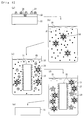
- Fig. 6 is a drawing showing a washing mechanism when washing is carried out by using the conventional washing solution.
- a contaminated semiconductor substrate 11 is immersed in a washing solution 15.
- a naturally oxidized film 12 formed on the surface of the semiconductor substrate 11 is removed by hydrofluoric acid (HF) whereby fine particles 13 and metal impurities 14 on the naturally oxidized film 12 as well as metal impurities 14 contained in the naturally oxidized film are shifted over to the washing solution 15.
- the washing solution 15 is an acidic solution having pH of 2 to 4 and containing 0.005 to 0.25 % by weight of hydrofluoric acid and 0.0001 to 0.1 % by weight of an organic acid, the surfaces of the fine particles 13 are charged to minus which is the same as that of the surface of the substrate 11.
- the metal impurities 14 liberated into the solution form a complex with organic acid molecules 16 to yield metal complex salts 17.
- This complex ion of the metal complex salt 17 is a minus ion.
- both of the surface potentials of the fine particles 13 and the metal impurities 14 become minus which is the same as that of the substrate 11 whereby adhesion or readhesion to the substrate can be prevented (Fig. 1(c)).
- a substrate 11 the surface of which is cleaned can be obtained (Fig. 1(d)).
- An invention according to Claim 5 relates to a method of washing a semiconductor substrate which comprises washing a semiconductor substrate with a washing solution containing 0.0001 to 0.1 % by weight of an organic acid and having pH of 2 to 4 while irradiating light with a wavelength of at least 500 nm.
- a contaminated semiconductor substrate is immersed in a washing solution and light with a wavelength of at least 500 nm is irradiated to the surface of the substrate.
- a washing solution By immersing the substrate in a washing solution, fine particles and metal impurities adhered to the substrate surface shift over to the washing solution.
- the washing solution is an acidic solution having pH of 2 to 4 and containing 0.0001 to 0.1 % by weight of an organic acid, the surfaces of the fine particles are charged to minus which is the same as that of the surface of the substrate.
- both of the surface potentials of the fine particles and the metal impurities become minus which is the same as that of the substrate whereby adhesion or re-adhesion to the substrate can be prevented.
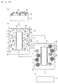
- An invention according to Claim 6 relates to a method of washing a semiconductor substrate which comprises washing a semiconductor substrate with a washing solution containing 0.0001 to 0.1 % by weight of an organic acid and 0.005 to 0.25 % by weight of hydrofluoric acid and having pH of 2 to 4 while irradiating light with a wavelength of at least 500 nm.
- a contaminated semi-conductor substrate 11 is immersed in a washing solution 15 and light 20 with a wavelength of at least 500 nm is irradiated to the surface of the substrate 11.
- hydrofluoric acid HF
- hydrofluoric acid removes a naturally oxidized film 12 formed on the surface of the semiconductor substrate 11, and fine particles 13 and metal impurities 14 on the naturally oxidized film 12 as well as metal impurities 14 contained in the naturally oxidized film are shifted over to the washing solution 15.
- the washing solution 15 is an acidic solution having pH of 2 to 4 and containing 0.005 to 0.25 % by weight of hydrofluoric acid and 0.0001 to 0.1 % by weight of an organic acid
- the surfaces of the fine particles 13 are charged to minus which is the same as that of the substrate surface 11.
- the metal impurities 14 liberated into the solution form a complex with organic acid molecules 16 to yield metal complex salts 17.
- This complex ion of the metal complex salt 17 is a minus ion.
- both of the surface potentials of the fine particles 13 and the metal impurities 14 become minus which is the same as that of the substrate 11 whereby adhesion or re-adhesion to the substrate can be prevented (Fig. 3(c)).
- An invention relating to Claim 7 is an invention according to Claim 5 or 6 and relates to a washing method wherein the organic acid is one or more organic acid selected from the group consisting of citric acid, succinic acid, EDTA, tartaric acid, salicylic acid, oxalic acid, acetic acid and formic acid.
- the organic acid is one or more organic acid selected from the group consisting of citric acid, succinic acid, EDTA, tartaric acid, salicylic acid, oxalic acid, acetic acid and formic acid.
- a method of Claim 8 relates to a washing method of a semiconductor substrate which contains a first washing step of washing a semiconductor substrate with a mixed solution of an organic acid and hydrofluoric acid with pH of 2 to 4, and a second washing step of washing said semiconductor substrate with an oxidizing solution.
- An invention relating to Claim 9 is an invention according to Claim 8, and is a method of washing a semiconductor substrate wherein the first washing step and the second washing step are each carried out at least twice.
- the surface of the substrate can be more cleaned.
- An invention according to Claim 10 is an invention relating to Claim 8 or 9, and is a method of washing a semiconductor substrate wherein the mixed solution of the first washing step contains 0.0001 to 0.1 % by weight of an organic acid and 0.005 to 0.25 % by weight of hydrofluoric acid.
- an organic acid and hydrofluoric acid in the above-mentioned concentration ranges are preferred.
- An invention according to Claim 11 is an invention relating to Claim 8 or 10, and is a method of washing a semiconductor substrate wherein the organic acid is one or more organic acid selected from the group consisting of citric acid, succinic acid, EDTA, tartaric acid, salicylic acid, oxalic acid, acetic acid and formic acid.
- the organic acid is one or more organic acid selected from the group consisting of citric acid, succinic acid, EDTA, tartaric acid, salicylic acid, oxalic acid, acetic acid and formic acid.
- organic acids enumerated have a complexing action of metal ions which are impurities contaminating the substrate.
- An invention according to Claim 12 is an invention relating to Claim 8 or 9, and is a method of washing a semiconductor substrate wherein the semiconductor substrate is subjected to ultrasonic washing with the mixed solution of the first washing step.
- the enumerated oxidizing solutions as mentioned above have actions of forming an oxidizing film at the surface of the substrate and of decomposing and removing organic acids or organic substances adhered to the surface of the substrate.
- a kind of an organic acid and a concentration thereof are determined depending on the kind of metal impurities to be removed.
- pH of the washing solution is 2 to 4.
- a concentration of the organic acid in the washing solution is 0.0001 to 0.1 % by weight, preferably 0.003 to 0.006 % by weight. If it is less than 0.0001 % by weight, a complexing action of metal impurity ions liberated from the surface of the substrate is not sufficient, while if it exceeds 0.1 % by weight, there is a disadvantage that an amount of fine particles adhered again will increase.
- organic acid of the present invention in addition to citric acid, succinic acid, EDTA, suitable for the present invention are tartaric acid, salicylic acid, oxalic acid, acetic acid, formic acid and the like.
- One or more kinds of acids are optionally selected from the above-mentioned organic acids depending on the metal elements constituting the metal impurities.
- a wavelength of light to be irradiated to the semiconductor substrate is at least 500 nm, preferably 400 to 900 nm, more preferably 600 to 700 nm. If it is less than 500 nm, a photocatalytic effect near to the surface of the semiconductor substrate is weak and the organic acid is not to be reduced and dissociated. Further, the higher the intensity of illumination of light is, the larger the irradiated dose is, so that the amount of bringing carriers into existence becomes large and reduction and dissociation of the organic acid are promoted. According the above, it can be considered that a complex ion-forming ability is improved and an effect of removing metal impurities near to the surface of the substrate is heightened.
- the mixed solution of the first washing step is preferably a washing solution relating to Claim 1.
- a dissolved ozone aqueous solution there may be mentioned a dissolved ozone aqueous solution, hydrogen peroxide solution or nitric acid.
- the dissolved ozone aqueous solution is preferred since it is high purity, high oxidizing power with a low concentration and easily available.
- An ozone concentration of the dissolved ozone aqueous solution is preferably 0.5 ppm or more. If it is less than 0.5 ppm, it is difficult to form a hydrophilic oxidized film on the surface of the substrate, and decomposition and removal effects of organic acids or organic substances adhered to the surface of the substrate are lowered. Since a dissolution limit of ozone to pure water is about 25 ppm, the ozone concentration of the dissolved ozone aqueous solution is more preferably 5 to 25 ppm.
- a silicon wafer is washed with a high concentration hydrofluoric acid, a naturally oxidized film on the surface of the wafer is removed and about 90 % of the surface of the wafer is terminated by hydrogen atom.
- a surface potential of the wafer is lowered and Cu, Ni, etc. which easily form a silicide accept an electron from the surface of the wafer to adhere to the surface of the wafer. Easiness of transfer the electron to an ion species such as a Cu ion, etc. from the surface of the wafer depends on an interfacial level in the solution.
- the interfacial level thereof is in the state near to that of the silicon wafer and electrons transfer through an electron transitional step so that this kind of a metal ion transfers to the surface of the wafer.
- adhesion and deposition phenomenon of the metal can be considered to be a complex system of the above-mentioned (a) as a base. That is, depending on how much amounts of hydrofluoric acid and an organic acid is present in the washing solution, the above-mentioned adhesion and deposition phenomenon will change. As a factor to determine the adhesion phenomenon, there are dissociation constant or ionization constant of the acid. When the constant is large, much amounts of protons are released and ion species of the acid increase. In the mixed system of hydrofluoric acid and an organic acid, it can be considered that an acid having a larger dissociation constant will be more predominantly dissociated.
- an amount of HF molecules which are not dissociated is also increased so that the naturally oxidized film is removed and a metal which easily forms a silicide such as Cu becomes to be easily adhered and deposited.
- a metal which easily forms a silicate such as Fe also becomes to be easily adhered and deposited.
- the metal such as Fe becomes to be easily formed due to increase in the concentration of the organic acid and an adhered amount to the surface of the wafer is lowered.
- citric acids As shown in Table 1, as an organic acid, 0.0006 % by weight, 0.006 % by weight and 0.06 % by weight of citric acids were mixed with pure water, respectively. To a citric acid aqueous solution containing 0.0006 % by weight of the acid were added 0.005 % by weight, 0.05 % by weight and 0.25 % by weight of hydrofluoric acid, respectively, to prepare washing solutions. Also, to a citric acid aqueous solution containing 0.006 % by weight of the acid were added 0.005 % by weight, 0.05 % by weight and 0.25 % by weight of hydrofluoric acid, respectively, to prepare washing solutions.
- EDTA ethylenediaminetetraacetic acids
- Table 2 As shown in Table 2, as an organic acid, 0.00008 % by weight and 0.0008 % by weight of ethylenediaminetetraacetic acids (EDTA) were mixed with pure water, respectively.
- EDTA aqueous solution containing 0.00008 % by weight of the acid were added 0.005 % by weight, 0.05 % by weight and 0.25 % by weight of hydrofluoric acid, respectively, to prepare washing solutions.
- washing solutions pH of the respective washing solutions are shown in Table 4.
- a silicon wafer cleaned by another SC1 solution was immersed, heated to 75 to 80 °C and maintained at 80 °C for 10 minutes. After this silicon wafer was rinsed by ultrapure water, the wafer was immersed in a mixed solution of H 2 O:
- a washing solution was prepared by adding 1 % by weight of hydrofluoric acid to a solution prepared by mixing 0.005 % by weight of ethylenediaminetetraacetic acid as an organic acid with pure water and pH of the solution was adjusted to 1.
- To the washing solution were added metal ions and fine particles which are similar to those used in Examples with the same amounts, and then a silicon wafer was immersed in the washing solution for 10 minutes. Thereafter, the silicon wafer was rinsed by ultrapure water in the same manner as in the above-mentioned Examples and dried.
- a washing solution was prepared by adding 0.05 % by weight of hydrofluoric acid to pure water. To the washing solution were added metal ions and fine particles which are similar to those used in Examples with the same amounts, and then a silicon wafer was immersed in the washing solution for 10 minutes. Thereafter, the silicon wafer was rinsed by ultrapure water in the same manner as in the above-mentioned Examples and dried.
- a washing solution was prepared by adding 0.25 % by weight of hydrofluoric acid to pure water. To the washing solution were added metal ions and fine particles which are similar to those used in Examples with the same amounts, and then a silicon wafer was immersed in the washing solution for 10 minutes. Thereafter, the silicon wafer was rinsed by ultrapure water in the same manner as in the above-mentioned Examples and dried.
- Metal impurities concentrations were measured on the surface of the silicon wafers after washing them with washing solutions prepared in Examples 1 to 4, 7 to 11, 14, 15, 17, 18, 21 to 23, 26 to 29, 31, 34, 35, 37 to 42 and Comparative example 1. These metal impurities concentrations were measured by dropping a mixed acid of hydrofluoric acid and nitric acid to the center portion of the silicon wafer after washing, and after developing liquid drops to cover the whole surface of the silicon wafer, and recovering the liquid drops to analyze them by atomic-absorption spectroscopy. The results are shown in Table 1 to Table 3.
- the number of remained particles on the surface of the respective wafers after washing them with each of washing solutions prepared in Examples 1, 4, 7, 12, 15, 18, 20, 22, 24, 26, 31 and Comparative examples 1 to 4 was measured.
- the number of remained particles was measured by counting particles with a particle size of 0.2 ⁇ m or more remained on the surface of the silicon wafer after washing with a particle counter. The results are shown in Table 4 and Table 5.
- a washing solution in which 0.006 % by weight of citric acid was added to pure water as an organic acid, having pH of 4.0 was prepared.
- the above-mentioned metal-contaminated silicon wafer was immersed in the washing solution at room temperature for 10 minutes, and irradiated light having an intensity of illumination of 100,000 lux and a wavelength of 500 nm to the surface of the silicon wafer. Thereafter, this silicon wafer was rinsed with ultrapure water for 10 minutes. According to the above procedure, peeling off of a naturally oxidized film on the surface of the wafer, complexing ions of metal impurities and control of each surface potential of the wafer, fine particles and metal impurities were carried out as mentioned above to clean the silicon wafer.
- Example 43 In the same manner as in Example 43 except for changing the wavelength of the light to be irradiated to 550 nm, a silicon wafer was washed.
- Example 43 In the same manner as in Example 43 except for changing the wavelength of the light to be irradiated to 600 nm, a silicon wafer was washed.
- Example 43 In the same manner as in Example 43 except for changing the wavelength of the light to be irradiated to 650 nm, a silicon wafer was washed.
- Example 43 In the same manner as in Example 43 except for changing the wavelength of the light to be irradiated to 450 nm, a silicon wafer was washed.
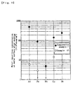
- Fe concentrations on the surfaces of the silicon wafers of Examples 43 to 46 and Comparative examples 5 and 6 after washing were examined. These metal impurities concentrations were measured by dropping a mixed acid of hydrofluoric acid and nitric acid to the center portion of the silicon wafer after washing, and after developing liquid drops to cover the whole surface of the silicon wafer, and recovering the liquid drops to analyze them by atomic-absorption spectroscopy. The results are shown in Fig. 4.
- a silicon wafer to the surface of which is adhered five metal of Al, Fe, Cu, Ni and Zn previously was prepared by the following method.
- This solution was raised to 80 °C, and after immersing the silicon wafer in the solution at 80 °C for 10 minutes, the wafer was rinsed for 10 minutes, then it was rinsed and water drops on the surface of the wafer were removed by centrifugal force and dried.
- a mixed solution was prepared by adding 0.05 % by weight of hydrofluoric acid to a solution in which 0.006 % by weight of citric acid was added to pure water as an organic acid, and adjusted to pH 3.0 was prepared.
- the mixed solution at room temperature was immersed the silicon wafer contaminated by the above-mentioned metal impurities and then washed under ultrasonic wave for 10 minutes. Thereafter, this silicon wafer was rinsed with ultrapure water for 10 minutes.
- this washed silicon wafer was immersed in a dissolved ozone aqueous solution with an ozone concentration of 8 ppm for 10 minutes. Thereafter, this silicon wafer was rinsed with ultrapure water for 10 minutes.
- the silicon wafer was washed again with the above-mentioned first washing step, and then washed again with the above-mentioned second washing step. That is, the first washing step and the second washing step were each carried out twice, respectively.
- Metal impurities concentrations on each surface of the respective silicon wafers after washing of Example 47 and Comparative example 7 were measured. This metal impurities concentrations were measured by dropping a mixed acid of hydrofluoric acid and nitric acid to the center portion of the silicon wafer after washing, and after developing liquid drops to cover the whole surface of the silicon wafer, and recovering the liquid drops to analyze them by atomic-absorption spectroscopy. The results are shown in Fig. 5. As clearly seen from Fig. 5, it can be found that, in the wafer of Example 47, except for Ni concentration which was the same level, there are good washing effects with regard to the other five kinds of metals with the order of one digit as compared with the wafer of Comparative example 7 according to the conventional RCA washing method. Particularly, four kinds of metals of Al, Fe, Ni and Zn were each 10 ⁇ 10 8 atoms/cm 2 or less. Incidentally, an arrow to downward of Fe and Ni means lower than detection limit.
- the photoirradiation brings minority carrier into existence near to the substrate surface, which reduces and dissociates an organic acid in the washing solution to make metal impurities into metal complex salts whereby an effect of removing metal impurities near to the surface of the substrate can be heightened.
- Chemical solution for washing is only one kind of an organic acid alone, or two kinds of hydrofluoric acid and an organic acid.
- washing method of the invention relating to Claim 8
- three actions of peeling a naturally oxidized film on the surface of the substrate, complex ionization of metal impurities, and control of each surface potential of the substrate, fine particles and metal impurities can be carried out in the first washing step to remove both of metal impurities and fine particles well from the semiconductor substrate, and then, in the second step, an oxidized film is formed on the surface of the substrate and simultaneously an organic acid or an organic material adhered to the surface of the substrate is decomposed and removed.
- both of metal impurities and fine particles can be well removed, and chemical solutions for washing may be only three kinds of hydrofluoric acid solution and an oxidizing solution.
Abstract
Description
| Hydrofluoric acid concentration (wt%) | Name of Organic acid | Organic acid concentration (wt%) | Metal impurity concentration | ||||||
| Fe | Ni | Zn | Cu | Al | |||||
| Example | 1 | 0.005 | Citric acid | 0.0006 | 4.5 x 10¹¹ | <1 x 10¹⁰ | <1 x 10¹⁰ | 4.3 x 10¹⁴ | <1 x 10¹⁰ |
| 2 | 0.006 | 2.6 x 10¹¹ | <1 x 10¹⁰ | <1 x 10¹⁰ | 2.6 x 10¹⁴ | <1 x 10¹⁰ | |||
| 3 | 0.06 | <1 x 10¹⁰ | <1 x 10¹⁰ | <1 x 10¹⁰ | 6.2 x 10¹² | <1 x 10¹⁰ | |||
| 4 | 0.05 | 0.0006 | <1 x 10¹⁰ | <1 x 10¹⁰ | <1 x 10¹⁰ | <1 x 10¹⁰ | <1 x 10¹⁰ | ||
| 5 | 0.006 | - | - | - | - | - | |||
| 6 | 0.06 | - | - | - | - | - | |||
| 7 | 0.25 | 0.0006 | <1 x 10¹⁰ | <1 x 10¹⁰ | <1 x 10¹⁰ | 2.7 x 10¹² | <1 x 10¹⁰ | ||
| 8 | 0.006 | <1 x 10¹⁰ | <1 x 10¹⁰ | <1 x 10¹⁰ | 3.0 x 10¹² | <1 x 10¹⁰ | |||
| 9 | 0.06 | <1 x 10¹⁰ | <1 x 10¹⁰ | <1 x 10¹⁰ | 2.9 x 10¹² | <1 x 10¹⁰ | |||
| 10 | 0.005 | Succinic acid | 0.00003 | <1 x 10¹⁰ | <1 x 10¹⁰ | <1 x 10¹⁰ | 7.3 x 10¹¹ | <1 x 10¹⁰ | |
| 11 | 0.003 | <1 x 10¹⁰ | <1 x 10¹⁰ | <1 x 10¹⁰ | 1 x 10¹² | <1 x 10¹⁰ | |||
| 12 | 0.05 | 0.00003 | - | - | - | - | - | ||
| 13 | 0.003 | - | - | - | - | - | |||
| 14 | 0.25 | 0.00003 | <1 x 10¹⁰ | <1 x 10¹⁰ | <1 x 10¹⁰ | 1.5 x 10¹¹ | - | ||
| 15 | 0.003 | <1 x 10¹⁰ | <1 x 10¹⁰ | <1 x 10¹⁰ | 1 x 10¹¹ | - |
| Hydrofluoric acid concentration (wt%) | Name of Organic acid | Organic acid concentration (wt%) | Metal impurity concentration | ||||||
| Fe | Ni | Zn | Cu | Al | |||||
| Example | 16 | 0.005 | EDTA | 0.00008 | - | - | - | - | - |
| 17 | 0.0008 | <1 x 10¹⁰ | <1 x 10¹⁰ | <1 x 10¹⁰ | <1 x 10¹⁰ | <1 x 10¹⁰ | |||
| 18 | 0.05 | 0.00008 | - | - | - | - | - | ||
| 19 | 0.0008 | 2 x 10¹⁰ | <1 x 10¹⁰ | <1 x 10¹⁰ | 2 x 10¹⁰ | <1 x 10¹⁰ | |||
| 20 | 0.25 | 0.00008 | - | - | - | - | - | ||
| 21 | 0.0008 | <1 x 10¹⁰ | <1 x 10¹⁰ | <1 x 10¹⁰ | 4 x 10¹¹ | <1 x 10¹⁰ | |||
| 22 | 0.005 | Tartaric acid | 0.0003 | <1 x 10¹⁰ | <1 x 10¹⁰ | <1 x 10¹⁰ | 1.1 x 10¹³ | <1 x 10¹⁰ | |
| 23 | 0.003 | <1 x 10¹⁰ | <1 x 10¹⁰ | <1 x 10¹⁰ | 7.7 x 10¹² | <1 x 10¹⁰ | |||
| 24 | 0.05 | 0.0003 | - | - | - | - | - | ||
| 25 | 0.003 | - | - | - | - | - | |||
| 26 | 0.25 | 0.0003 | <1 x 10¹⁰ | <1 x 10¹⁰ | <1 x 10¹⁰ | 1.8 x 10¹² | <1 x 10¹⁰ | ||
| 27 | 0.003 | <1 x 10¹⁰ | <1 x 10¹⁰ | <1 x 10¹⁰ | 4.3 x 10¹¹ | <1 x 10¹⁰ |
| Hydrofluoric acid concentration (wt%) | Name of Organic acid | Organic acid concentration (wt%) | Metal impurity concentration | ||||||
| Fe | Ni | Zn | Cu | Al | |||||
| Example | 28 | 0.005 | Oxalic acid | 0.00027 | - | - | - | 4.5 x 10¹¹ | <1 x 10¹⁰ |
| 29 | 0.0027 | <1 x 10¹⁰ | <1 x 10¹⁰ | <1 x 10¹⁰ | <1 x 10¹⁰ | <1 x 10¹⁰ | |||
| 30 | 0.027 | - | - | - | - | - | |||
| 31 | 0.05 | 0.00027 | - | - | - | 1.6 x 10¹³ | 1.2 x 10¹⁰ | ||
| 32 | 0.0027 | - | - | - | - | - | |||
| 33 | 0.027 | - | - | - | - | - | |||
| 34 | 0.25 | 0.00027 | 2.6 1010 | x <1 x 10¹⁰ | <1 x 10¹⁰ | 4.8 x 10¹³ | <1 x 10¹⁰ | ||
| 35 | 0.0027 | - | <1 x 10¹⁰ | <1 x 10¹⁰ | 4.3 x 10¹² | <1 x 10¹⁰ | |||
| 36 | 0.027 | - | - | - | - | - | |||
| 37 | 0.005 | Acetic acid | 0.00018 | <1 x 10¹⁰ | <1 x 10¹⁰ | <1 x 10¹⁰ | 9 x 10¹² | 4.9 x 10¹⁰ | |
| 38 | 0.018 | <1 x 10¹⁰ | <1 x 10¹⁰ | <1 x 10¹⁰ | 1.5 x 10¹² | <1 x 10¹⁰ | |||
| 39 | 0.05 | 0.00018 | <1 x 10¹⁰ | <1 x 10¹⁰ | <1 x 10¹⁰ | 5.2 x 10¹¹ | 1.3 x 10¹⁰ | ||
| 40 | 0.018 | <1 x 10¹⁰ | <1 x 10¹⁰ | <1 x 10¹⁰ | 4.7 x 10¹¹ | 1 x 10¹⁰ | |||
| 41 | 0.25 | 0.00018 | <1 x 10¹⁰ | <1 x 10¹⁰ | <1 x 10¹⁰ | 1.1 x 10¹² | <1 x 10¹⁰ | ||
| 42 | 0.018 | <1 x 10¹⁰ | <1 x 10¹⁰ | <1 x 10¹⁰ | 5.4 x 10¹¹ | <1 x 10¹⁰ | |||
| Comparative example | 1 | (RCR Washing) | <1 x 10¹⁰ | <1 x 10¹⁰ | <1 x 10¹⁰ | 1.5 x 10¹¹ | 4.0 x 10¹⁰ |
| Hydrofluoric acid concentration (wt%) | Name of organic acid | Organic acid concentration (wt%) | pH | Adhered number of particles having 0.2 µm or more | ||
| Example | 1 | 0.005 | Citric acid | 0.0006 | 3.0 | 12 |
| 2 | 0.006 | 2.9 | ― | |||
| 3 | 0.06 | 2.3 | ― | |||
| 4 | 0.05 | 0.0006 | 2.8 | 15 | ||
| 5 | 0.006 | 2.4 | ― | |||
| 6 | 0.06 | 2.2 | ― | |||
| 7 | 0.25 | 0.0006 | 2.0 | 64 | ||
| 8 | 0.006 | 2.0 | ― | |||
| 9 | 0.06 | 2.0 | ― | |||
| 10 | 0.005 | Succinic acid | 0.00003 | 3.2 | ― | |
| 11 | 0.003 | 3.2 | ― | |||
| 12 | 0.05 | 0.00003 | 2.7 | 51 | ||
| 13 | 0.003 | 3.4 | ― | |||
| 14 | 0.25 | 0.00003 | 2.0 | ― | ||
| 15 | 0.003 | 2.0 | 72 | |||
| 16 | 0.005 | EDTA | 0.00008 | 3.1 | ― | |
| 17 | 0.0008 | 3.0 | ― | |||
| 18 | 0.05 | 0.00008 | 2.4 | 8 | ||
| 19 | 0.0008 | 2.3 | ― | |||
| 20 | 0.25 | 0.00008 | 2.0 | 16 | ||
| 21 | 0.0008 | 2.0 | ― | |||
| 22 | 0.005 | Tartaric acid | 0.0003 | 3.1 | 49 | |
| 23 | 0.003 | 2.4 | ― | |||
| 24 | 0.05 | 0.0003 | 2.8 | 41 | ||
| 25 | 0.003 | 2.1 | ― | |||
| 26 | 0.25 | 0.0003 | 2.0 | 78 | ||
| 27 | 0.003 | 2.0 | ― |
| Hydrofluoric acid concentration (wt%) | Name of organic acid | Organic acid concentration (wt%) | pH | Adhered number of particles having 0.2 µm or more | ||
| Example | 28 | 0.005 | Oxalic acid | 0.00027 | 3.0 | ― |
| 29 | 0.0027 | 2.6 | ― | |||
| 30 | 0.027 | 2.0 | ― | |||
| 31 | 0.05 | 0.00027 | 2.9 | 43 | ||
| 32 | 0.0027 | 2.7 | ― | |||
| 33 | 0.027 | 2.4 | ― | |||
| 34 | 0.25 | 0.00027 | 2.0 | ― | ||
| 35 | 0.0027 | 2.0 | ― | |||
| 36 | 0.027 | 2.0 | ― | |||
| 37 | 0.005 | Succinic acid | 0.00018 | 3.1 | ― | |
| 38 | 0.0018 | 2.9 | ― | |||
| 39 | 0.05 | 0.00018 | 2.9 | ― | ||
| 40 | 0.0018 | 2.8 | ― | |||
| 41 | 0.25 | 0.00018 | 2.0 | ― | ||
| 42 | 0.0018 | 2.0 | ― | |||
| Comparative example | 1 | (RCA washing) | ― | 10 | ||
| 2 | 1.00 | EDTA | 0.005 | 1.0 | 2123 | |
| 3 | 0.05 | None | ― | ― | 218 | |
| 4 | 0.25 | ― | ― | 1542 |
Claims (13)
- A washing solution of a semiconductor substrate comprising 0.0001 to 0.1 % by weight of an organic acid and 0.005 to 0.25 % by weight of hydrofluoric acid and having pH of 2 to 4.
- The washing solution of a semiconductor substrate according to Claim 1, wherein said organic acid is one or more organic acid selected from the group consisting of citric acid, succinic acid, ethylenediaminetetraacetic acid, tartaric acid, salicylic acid, oxalic acid, acetic acid and formic acid.
- A method of washing a semiconductor substrate which comprises washing a semiconductor substrate with a washing solution containing 0.0001 to 0.1 % by weight of an organic acid and 0.005 to 0.25 % by weight of hydrofluoric acid and having pH of 2 to 4.
- The method of washing a semiconductor substrate according to Claim 3, wherein the organic acid is one or more organic acid selected from the group consisting of citric acid, succinic acid, EDTA, tartaric acid, salicylic acid, oxalic acid, acetic acid and formic acid.
- A method of washing a semiconductor substrate which comprises washing a semiconductor substrate with a washing solution containing 0.0001 to 0.1 % by weight of an organic acid and having pH of 2 to 4 while irradiating light with a wavelength of at least 500 nm.
- A method of washing a semiconductor substrate which comprises washing a semiconductor substrate with a washing solution containing 0.0001 to 0.1 % by weight of an organic acid and 0.005 to 0.25 % by weight of hydrofluoric acid and having pH of 2 to 4 while irradiating light with a wavelength of at least 500 nm.
- The method of washing a semiconductor substrate according to Claim 5 or 6, wherein the organic acid is one or more organic acid selected from the group consisting of citric acid, succinic acid, EDTA, tartaric acid, salicylic acid, oxalic acid, acetic acid and formic acid.
- A method of washing a semiconductor substrate which comprisesa first washing step of washing a semiconductor substrate with a mixed solution of an organic acid and hydrofluoric acid with pH of 2 to 4, anda second washing step of washing said semiconductor substrate with an oxidizing solution.
- The method of washing a semiconductor substrate according to Claim 8, wherein the first washing step and the second washing step are each carried out at least twice.
- A method of washing a semiconductor substrate according to Claim 8 or 9, wherein the mixed solution of the first washing step contains 0.0001 to 0.1 % by weight of an organic acid and 0.005 to 0.25 % by weight of hydrofluoric acid.
- The method of washing a semiconductor substrate according to Claim 8 or 10, wherein the organic acid is one or more organic acid selected from the group consisting of citric acid, succinic acid, EDTA, tartaric acid, salicylic acid, oxalic acid, acetic acid and formic acid.
- The method of washing a semiconductor substrate according to Claim 8 or 9, wherein the semiconductor substrate is subjected to ultrasonic washing with the mixed solution of the first washing step.
- The method of washing a semiconductor substrate according to Claim 8 or 9, wherein the oxidizing solution of the second washing step is a dissolved ozone aqueous solution, hydrogen peroxide solution or nitric acid.
Applications Claiming Priority (6)
| Application Number | Priority Date | Filing Date | Title |
|---|---|---|---|
| JP00561297A JP3354822B2 (en) | 1997-01-16 | 1997-01-16 | Semiconductor substrate cleaning method |
| JP561197A JPH10209100A (en) | 1997-01-16 | 1997-01-16 | Cleaning method of semiconductor substrate |
| JP561097 | 1997-01-16 | ||
| JP5612/97 | 1997-01-16 | ||
| JP5610/97 | 1997-01-16 | ||
| JP5611/97 | 1997-01-16 |
Publications (3)
| Publication Number | Publication Date |
|---|---|
| EP0859404A2 true EP0859404A2 (en) | 1998-08-19 |
| EP0859404A3 EP0859404A3 (en) | 1999-05-26 |
| EP0859404B1 EP0859404B1 (en) | 2014-04-02 |
Family
ID=27276827
Family Applications (1)
| Application Number | Title | Priority Date | Filing Date |
|---|---|---|---|
| EP98100625.7A Expired - Lifetime EP0859404B1 (en) | 1997-01-16 | 1998-01-15 | Washing solution of semiconductor substrate and washing method using the same |
Country Status (4)
| Country | Link |
|---|---|
| US (1) | US6296714B1 (en) |
| EP (1) | EP0859404B1 (en) |
| KR (1) | KR100279911B1 (en) |
| TW (1) | TW463261B (en) |
Cited By (14)
| Publication number | Priority date | Publication date | Assignee | Title |
|---|---|---|---|---|
| WO1999021220A1 (en) * | 1997-10-21 | 1999-04-29 | Ontrak Systems, Inc. | Methods and apparatus for cleaning semiconductor substrates after polishing of copper film |
| EP0982765A2 (en) * | 1998-08-28 | 2000-03-01 | Mitsubishi Materials Silicon Corporation | Cleaning method of semiconductor substrate |
| EP1005072A1 (en) * | 1998-11-19 | 2000-05-31 | Wacker Siltronic Gesellschaft für Halbleitermaterialien Aktiengesellschaft | Method for wet-chemical treatment of semiconductor substrates |
| FR2796319A1 (en) * | 1999-07-13 | 2001-01-19 | Lionel Girardie | Powerful cleaning process used in modern microelectronic component treatments employs solution of hydrofluoric and hydrochloric acids in ultra-pure water, with citric acid |
| US6303551B1 (en) | 1997-10-21 | 2001-10-16 | Lam Research Corporation | Cleaning solution and method for cleaning semiconductor substrates after polishing of cooper film |
| US6358847B1 (en) | 1999-03-31 | 2002-03-19 | Lam Research Corporation | Method for enabling conventional wire bonding to copper-based bond pad features |
| EP1189265A1 (en) * | 2000-03-17 | 2002-03-20 | Shin-Etsu Handotai Co., Ltd | Water for storing silicon wafers and storing method |
| EP1196943A1 (en) * | 1999-05-26 | 2002-04-17 | Ashland Inc. | Process for removing contaminant from a surface and composition useful therefor |
| US6479443B1 (en) | 1997-10-21 | 2002-11-12 | Lam Research Corporation | Cleaning solution and method for cleaning semiconductor substrates after polishing of copper film |
| US6593282B1 (en) | 1997-10-21 | 2003-07-15 | Lam Research Corporation | Cleaning solutions for semiconductor substrates after polishing of copper film |
| EP1536291A1 (en) * | 2002-08-22 | 2005-06-01 | Daikin Industries, Ltd. | Removing solution |
| WO2007045269A1 (en) * | 2005-10-21 | 2007-04-26 | Freescale Semiconductor, Inc. | Method for cleaning a semiconductor structure and chemistry thereof |
| US7312159B2 (en) | 2000-08-31 | 2007-12-25 | Micron Technology, Inc. | Compositions for dissolution of low-k dielectric films, and methods of use |
| WO2008053705A2 (en) * | 2006-10-24 | 2008-05-08 | Asahi Glass Company, Limited | Method for removing foreign matters from substrate surface |
Families Citing this family (12)
| Publication number | Priority date | Publication date | Assignee | Title |
|---|---|---|---|---|
| JP3510562B2 (en) * | 2000-04-28 | 2004-03-29 | Necエレクトロニクス株式会社 | Semiconductor device manufacturing method and processing apparatus |
| EP1389496A1 (en) * | 2001-05-22 | 2004-02-18 | Mitsubishi Chemical Corporation | Method for cleaning surface of substrate |
| US6610599B1 (en) * | 2002-06-19 | 2003-08-26 | Lucent Technologies Inc. | Removal of metal veils from via holes |
| JP2004253775A (en) * | 2003-01-31 | 2004-09-09 | Nec Electronics Corp | Chemical mechanical polishing method |
| SG129274A1 (en) * | 2003-02-19 | 2007-02-26 | Mitsubishi Gas Chemical Co | Cleaaning solution and cleaning process using the solution |
| KR100672933B1 (en) * | 2003-06-04 | 2007-01-23 | 삼성전자주식회사 | Cleaning solution and cleaning method in a semiconductor device |
| JP5533624B2 (en) * | 2010-12-16 | 2014-06-25 | 信越半導体株式会社 | Semiconductor wafer cleaning method |
| WO2018061670A1 (en) * | 2016-09-29 | 2018-04-05 | 富士フイルム株式会社 | Processing solution, and method for processing laminate |
| JP6970675B2 (en) * | 2016-09-29 | 2021-11-24 | 富士フイルム株式会社 | Treatment liquid and laminating body treatment method |
| FR3068509B1 (en) * | 2017-06-30 | 2020-02-28 | Technic France | CHEMICAL CLEANING COMPOSITION FOR REMOVING AN AMORPHOUS PASSIVATION LAYER ON THE SURFACE OF CRYSTALLINE MATERIALS |
| CN109427543B (en) * | 2017-08-31 | 2022-09-23 | 胜高股份有限公司 | Method for cleaning silicon wafer |
| CN113257659B (en) * | 2021-04-09 | 2022-09-23 | 上海中欣晶圆半导体科技有限公司 | Method for reducing heavy metal and haze defects through BSD (back washing) post-cleaning |
Citations (9)
| Publication number | Priority date | Publication date | Assignee | Title |
|---|---|---|---|---|
| US4181623A (en) * | 1977-03-15 | 1980-01-01 | Colgate-Palmolive Company | Cleaning compositions |
| EP0571950A2 (en) * | 1992-05-29 | 1993-12-01 | Texas Instruments Incorporated | Removal of metal contamination |
| WO1994027314A1 (en) * | 1993-05-13 | 1994-11-24 | Interuniversitair Microelektronica Centrum | Method for semiconductor processing using mixtures of hf and carboxylic acid |
| US5382296A (en) * | 1991-02-27 | 1995-01-17 | Okmetic Oy | Method for cleaning semiconductor products |
| EP0674343A2 (en) * | 1994-03-25 | 1995-09-27 | Shin-Etsu Handotai Company Limited | Method for storing silicon wafers |
| FR2722511A1 (en) * | 1994-07-15 | 1996-01-19 | Ontrak Systems Inc | Metal contaminant removal during substrate cleaning |
| DE19521389A1 (en) * | 1994-12-06 | 1996-06-13 | Mitsubishi Electric Corp | Semiconductor integrated circuit mfg. |
| WO1996026538A1 (en) * | 1995-02-21 | 1996-08-29 | Advanced Micro Devices, Inc. | Chemical solutions for removing metal-compound contaminants from wafers after cmp and the method of wafer cleaning |
| DE19515024A1 (en) * | 1995-04-24 | 1996-10-31 | Wacker Siltronic Halbleitermat | Aq. compsn., for cleaning semi-conductor discs, esp. silicon |
Family Cites Families (5)
| Publication number | Priority date | Publication date | Assignee | Title |
|---|---|---|---|---|
| US5409544A (en) * | 1990-08-20 | 1995-04-25 | Hitachi, Ltd. | Method of controlling adhesion of fine particles to an object in liquid |
| US5695569A (en) * | 1991-02-28 | 1997-12-09 | Texas Instruments Incorporated | Removal of metal contamination |
| JP2652320B2 (en) * | 1993-03-31 | 1997-09-10 | 住友シチックス株式会社 | Silicon wafer cleaning method |
| JP2914555B2 (en) * | 1994-08-30 | 1999-07-05 | 信越半導体株式会社 | Cleaning method for semiconductor silicon wafer |
| US5714203A (en) * | 1995-08-23 | 1998-02-03 | Ictop Entwicklungs Gmbh | Procedure for the drying of silicon |
-
1998
- 1998-01-08 US US09/004,199 patent/US6296714B1/en not_active Expired - Lifetime
- 1998-01-09 TW TW087100206A patent/TW463261B/en not_active IP Right Cessation
- 1998-01-15 KR KR1019980000992A patent/KR100279911B1/en not_active IP Right Cessation
- 1998-01-15 EP EP98100625.7A patent/EP0859404B1/en not_active Expired - Lifetime
Patent Citations (9)
| Publication number | Priority date | Publication date | Assignee | Title |
|---|---|---|---|---|
| US4181623A (en) * | 1977-03-15 | 1980-01-01 | Colgate-Palmolive Company | Cleaning compositions |
| US5382296A (en) * | 1991-02-27 | 1995-01-17 | Okmetic Oy | Method for cleaning semiconductor products |
| EP0571950A2 (en) * | 1992-05-29 | 1993-12-01 | Texas Instruments Incorporated | Removal of metal contamination |
| WO1994027314A1 (en) * | 1993-05-13 | 1994-11-24 | Interuniversitair Microelektronica Centrum | Method for semiconductor processing using mixtures of hf and carboxylic acid |
| EP0674343A2 (en) * | 1994-03-25 | 1995-09-27 | Shin-Etsu Handotai Company Limited | Method for storing silicon wafers |
| FR2722511A1 (en) * | 1994-07-15 | 1996-01-19 | Ontrak Systems Inc | Metal contaminant removal during substrate cleaning |
| DE19521389A1 (en) * | 1994-12-06 | 1996-06-13 | Mitsubishi Electric Corp | Semiconductor integrated circuit mfg. |
| WO1996026538A1 (en) * | 1995-02-21 | 1996-08-29 | Advanced Micro Devices, Inc. | Chemical solutions for removing metal-compound contaminants from wafers after cmp and the method of wafer cleaning |
| DE19515024A1 (en) * | 1995-04-24 | 1996-10-31 | Wacker Siltronic Halbleitermat | Aq. compsn., for cleaning semi-conductor discs, esp. silicon |
Non-Patent Citations (2)
| Title |
|---|
| ANONYMOUS: "Silicon Surface Cleaning Process. October 1977." IBM TECHNICAL DISCLOSURE BULLETIN, vol. 20, no. 5, October 1977, pages 1746-1747, XP002095501 New York, US * |
| PATENT ABSTRACTS OF JAPAN vol. 095, no. 001, 28 February 1995 & JP 06 291099 A (SUMITOMO SITIX CORP), 18 October 1994 * |
Cited By (33)
| Publication number | Priority date | Publication date | Assignee | Title |
|---|---|---|---|---|
| WO1999021220A1 (en) * | 1997-10-21 | 1999-04-29 | Ontrak Systems, Inc. | Methods and apparatus for cleaning semiconductor substrates after polishing of copper film |
| US6162301A (en) * | 1997-10-21 | 2000-12-19 | Lam Research Corporation | Methods and apparatus for cleaning semiconductor substrates after polishing of copper film |
| US6165956A (en) * | 1997-10-21 | 2000-12-26 | Lam Research Corporation | Methods and apparatus for cleaning semiconductor substrates after polishing of copper film |
| US6593282B1 (en) | 1997-10-21 | 2003-07-15 | Lam Research Corporation | Cleaning solutions for semiconductor substrates after polishing of copper film |
| US6479443B1 (en) | 1997-10-21 | 2002-11-12 | Lam Research Corporation | Cleaning solution and method for cleaning semiconductor substrates after polishing of copper film |
| US6303551B1 (en) | 1997-10-21 | 2001-10-16 | Lam Research Corporation | Cleaning solution and method for cleaning semiconductor substrates after polishing of cooper film |
| KR100340274B1 (en) * | 1998-08-28 | 2002-06-12 | 가와이 겐이찌 | Cleaning Method of Semiconductor Substrate |
| EP0982765A2 (en) * | 1998-08-28 | 2000-03-01 | Mitsubishi Materials Silicon Corporation | Cleaning method of semiconductor substrate |
| EP0982765A3 (en) * | 1998-08-28 | 2000-04-19 | Mitsubishi Materials Silicon Corporation | Cleaning method of semiconductor substrate |
| US7172975B2 (en) | 1998-11-19 | 2007-02-06 | Siltronic Ag | Process for the wet chemical treatment of semiconductor wafers |
| SG83159A1 (en) * | 1998-11-19 | 2001-09-18 | Wacker Siltronic Halbleitermat | Process for the wet chemical treatment of semiconductor wafers |
| EP1005072A1 (en) * | 1998-11-19 | 2000-05-31 | Wacker Siltronic Gesellschaft für Halbleitermaterialien Aktiengesellschaft | Method for wet-chemical treatment of semiconductor substrates |
| US6358847B1 (en) | 1999-03-31 | 2002-03-19 | Lam Research Corporation | Method for enabling conventional wire bonding to copper-based bond pad features |
| US6610601B2 (en) | 1999-03-31 | 2003-08-26 | Lam Research Corporation | Bond pad and wire bond |
| EP1196943A1 (en) * | 1999-05-26 | 2002-04-17 | Ashland Inc. | Process for removing contaminant from a surface and composition useful therefor |
| EP1196943A4 (en) * | 1999-05-26 | 2007-01-17 | Air Prod & Chem | Process for removing contaminant from a surface and composition useful therefor |
| FR2796319A1 (en) * | 1999-07-13 | 2001-01-19 | Lionel Girardie | Powerful cleaning process used in modern microelectronic component treatments employs solution of hydrofluoric and hydrochloric acids in ultra-pure water, with citric acid |
| EP1189265A4 (en) * | 2000-03-17 | 2007-04-25 | Shinetsu Handotai Kk | Water for storing silicon wafers and storing method |
| EP1189265A1 (en) * | 2000-03-17 | 2002-03-20 | Shin-Etsu Handotai Co., Ltd | Water for storing silicon wafers and storing method |
| US7432214B2 (en) | 2000-08-31 | 2008-10-07 | Micron Technology, Inc. | Compositions for dissolution of low-k dielectric film, and methods of use |
| US8951433B2 (en) | 2000-08-31 | 2015-02-10 | Micron Technology, Inc. | Compositions for use in semiconductor devices |
| US7312159B2 (en) | 2000-08-31 | 2007-12-25 | Micron Technology, Inc. | Compositions for dissolution of low-k dielectric films, and methods of use |
| US8632692B2 (en) | 2000-08-31 | 2014-01-21 | Micron Technology, Inc. | Compositions for use in semiconductor devices |
| US7399424B2 (en) * | 2000-08-31 | 2008-07-15 | Micron Technology, Inc. | Compositions for dissolution of low-k dielectric films, and methods of use |
| US8142673B2 (en) | 2000-08-31 | 2012-03-27 | Micron Technology, Inc. | Compositions for dissolution of low-k dielectric films, and methods of use |
| US7521373B2 (en) | 2000-08-31 | 2009-04-21 | Micron Technology, Inc. | Compositions for dissolution of low-k dielectric films, and methods of use |
| EP1536291A1 (en) * | 2002-08-22 | 2005-06-01 | Daikin Industries, Ltd. | Removing solution |
| US7833957B2 (en) | 2002-08-22 | 2010-11-16 | Daikin Industries, Ltd. | Removing solution |
| EP1536291A4 (en) * | 2002-08-22 | 2008-08-06 | Daikin Ind Ltd | Removing solution |
| WO2007045269A1 (en) * | 2005-10-21 | 2007-04-26 | Freescale Semiconductor, Inc. | Method for cleaning a semiconductor structure and chemistry thereof |
| WO2008053705A3 (en) * | 2006-10-24 | 2008-09-18 | Asahi Glass Co Ltd | Method for removing foreign matters from substrate surface |
| US8052797B2 (en) | 2006-10-24 | 2011-11-08 | Asahi Glass Company, Limited | Method for removing foreign matter from substrate surface |
| WO2008053705A2 (en) * | 2006-10-24 | 2008-05-08 | Asahi Glass Company, Limited | Method for removing foreign matters from substrate surface |
Also Published As
| Publication number | Publication date |
|---|---|
| TW463261B (en) | 2001-11-11 |
| EP0859404A3 (en) | 1999-05-26 |
| EP0859404B1 (en) | 2014-04-02 |
| KR19980070530A (en) | 1998-10-26 |
| KR100279911B1 (en) | 2001-09-06 |
| US6296714B1 (en) | 2001-10-02 |
Similar Documents
| Publication | Publication Date | Title |
|---|---|---|
| US6296714B1 (en) | Washing solution of semiconductor substrate and washing method using the same | |
| KR100340274B1 (en) | Cleaning Method of Semiconductor Substrate | |
| KR0158008B1 (en) | Method of cleaning semiconductor substrate using an aqueous acid solution | |
| JP2581268B2 (en) | Semiconductor substrate processing method | |
| EP0789071B1 (en) | Method for treating surface of substrate and surface treatment composition therefor | |
| JPH03219000A (en) | Etching method and washing method for silicon wafer | |
| JP3957264B2 (en) | Semiconductor substrate cleaning method | |
| RU2329298C2 (en) | Treatment of semiconductor surfaces and mixture used in process | |
| JP3174823B2 (en) | Silicon wafer cleaning method | |
| JP3239998B2 (en) | Semiconductor substrate cleaning method | |
| JP2776583B2 (en) | Semiconductor substrate processing solution and processing method | |
| JPH0831837A (en) | Deposition method of polysilicon for eg | |
| RU2319252C2 (en) | Method for cleaning silicon substrate surfaces | |
| JP2002100599A (en) | Washing method for silicon wafer | |
| JP2001326209A (en) | Method for treating surface of silicon substrate | |
| JPH05166777A (en) | Washing of semiconductor wafer | |
| JP2749938B2 (en) | Cleaning method for semiconductor wafer | |
| JP3767694B2 (en) | Semiconductor substrate cleaning method | |
| JP3354822B2 (en) | Semiconductor substrate cleaning method | |
| JPH10209100A (en) | Cleaning method of semiconductor substrate | |
| JP2001217215A (en) | Composition and method for treating surface of semiconductor substrate | |
| JP2001244228A (en) | Liquid and method for washing semiconductor substrate | |
| JP4026384B2 (en) | Semiconductor substrate cleaning method | |
| JP2000277473A (en) | Cleaning method of silicon wafer | |
| JP2000049132A (en) | Method of cleaning semiconductor substrate |
Legal Events
| Date | Code | Title | Description |
|---|---|---|---|
| PUAI | Public reference made under article 153(3) epc to a published international application that has entered the european phase |
Free format text: ORIGINAL CODE: 0009012 |
|
| AK | Designated contracting states |
Kind code of ref document: A2 Designated state(s): DE FR GB |
|
| AX | Request for extension of the european patent |
Free format text: AL;LT;LV;MK;RO;SI |
|
| PUAL | Search report despatched |
Free format text: ORIGINAL CODE: 0009013 |
|
| AK | Designated contracting states |
Kind code of ref document: A3 Designated state(s): AT BE CH DE DK ES FI FR GB GR IE IT LI LU MC NL PT SE |
|
| AX | Request for extension of the european patent |
Free format text: AL;LT;LV;MK;RO;SI |
|
| 17P | Request for examination filed |
Effective date: 19990830 |
|
| AKX | Designation fees paid |
Free format text: DE FR GB |
|
| 17Q | First examination report despatched |
Effective date: 20070917 |
|
| GRAP | Despatch of communication of intention to grant a patent |
Free format text: ORIGINAL CODE: EPIDOSNIGR1 |
|
| RIC1 | Information provided on ipc code assigned before grant |
Ipc: C11D 7/00 20060101ALI20130925BHEP Ipc: H01L 21/02 20060101ALI20130925BHEP Ipc: H01L 21/306 20060101AFI20130925BHEP |
|
| INTG | Intention to grant announced |
Effective date: 20131031 |
|
| GRAS | Grant fee paid |
Free format text: ORIGINAL CODE: EPIDOSNIGR3 |
|
| GRAA | (expected) grant |
Free format text: ORIGINAL CODE: 0009210 |
|
| AK | Designated contracting states |
Kind code of ref document: B1 Designated state(s): DE FR GB |
|
| REG | Reference to a national code |
Ref country code: GB Ref legal event code: FG4D |
|
| REG | Reference to a national code |
Ref country code: DE Ref legal event code: R096 Ref document number: 69843220 Country of ref document: DE Effective date: 20140508 |
|
| REG | Reference to a national code |
Ref country code: DE Ref legal event code: R097 Ref document number: 69843220 Country of ref document: DE |
|
| PLBE | No opposition filed within time limit |
Free format text: ORIGINAL CODE: 0009261 |
|
| STAA | Information on the status of an ep patent application or granted ep patent |
Free format text: STATUS: NO OPPOSITION FILED WITHIN TIME LIMIT |
|
| 26N | No opposition filed |
Effective date: 20150106 |
|
| REG | Reference to a national code |
Ref country code: DE Ref legal event code: R097 Ref document number: 69843220 Country of ref document: DE Effective date: 20150106 |
|
| REG | Reference to a national code |
Ref country code: FR Ref legal event code: PLFP Year of fee payment: 19 |
|
| REG | Reference to a national code |
Ref country code: FR Ref legal event code: PLFP Year of fee payment: 20 |
|
| PGFP | Annual fee paid to national office [announced via postgrant information from national office to epo] |
Ref country code: DE Payment date: 20170120 Year of fee payment: 20 Ref country code: FR Payment date: 20170120 Year of fee payment: 20 |
|
| PGFP | Annual fee paid to national office [announced via postgrant information from national office to epo] |
Ref country code: GB Payment date: 20170119 Year of fee payment: 20 |
|
| REG | Reference to a national code |
Ref country code: DE Ref legal event code: R071 Ref document number: 69843220 Country of ref document: DE |
|
| REG | Reference to a national code |
Ref country code: GB Ref legal event code: PE20 Expiry date: 20180114 |
|
| PG25 | Lapsed in a contracting state [announced via postgrant information from national office to epo] |
Ref country code: GB Free format text: LAPSE BECAUSE OF EXPIRATION OF PROTECTION Effective date: 20180114 |