The present invention relates to an image
processing apparatus for processing colour image
data.
In a known digital copying machine, an original
image is illuminated by a halogen lamp or other light
source. Light reflected from the original image is
photoelectrically transferred by a charge coupled
device (CCD) or any other solid-state imaging device
and converted into a digital signal. After that, a
given corrective operation is applied to the digital
signal. Finally, the corrected signal is fed to a
laser beam printer, liquid crystal printer, thermal
printer, ink-jet printer or other recording apparatus
to record the image.
Digital copying machines of this type are expected
to produce documents containing more abundant
information. Copying machines, having a multi-colour
laser beam printer equipped with multiple colour
developing units, which copy an original image by
changing colours from area to area, have been
developed in recent years.
However, the aforesaid copying machines, arranged
to form images by changing colours from area to area,
are equipped with many developing devices, therefore,
the mechanisms are complex. Furthermore, since high
precision is required for image positioning, each
product is very expensive.
Copying machines using a multi-colour ink-jet
printer pose the same problem.
The specification of US Patent No 4,369,461
discloses a copying machine in which colour
information read from an original document is assessed
to detect particular colours. Thereafter, graphic
patterns such as an oblique line pattern, a
longitudinal line pattern, a lateral line pattern, a
waveform line pattern, a small circle pattern or a
dot pattern are synthesized on a monochrome image so
as to respresent said colours. Thus, the copying
machine is able to express the differences in colour
among the pixels in the colour images of an original,
using a low-price printer. However, this kind of
copying apparatus cannot visualize actual colour
information, about the colours of pixels in the colour
images of an original document.
In the aforesaid known copying machines, graphic
patterns, associated with colour information of
original images, are preprogrammed in the machine and
only a limited number of graphic patterns are
available. There is no facility for users to specify
desired graphic patterns, depending on the colour
information of the original.
An object of the present invention is to provide
an improved image processing apparatus.
Another object of the invention is to provide an
image processing apparatus which employs a low-priced
monochrome printer, while producing images which
permit effortless and accurate recognition of the
colours of pixels in the original images.
Another object of the invention is to provide an
image processing apparatus for clearly displaying
characters representing the names of colours, in areas
of white background.
Another object of the invention is to provide an
image processing apparatus for permitting quick
recognition of the differences of colours among pixels
in the image of an original.
Another object of the invention is to provide an
image processing apparatus for eliminating a
suggestion of incompatibility, occurring when
character patterns, not included in an original image,
are appended to an output monochrome image and
outputting a collation table for the character
patterns and graphic patterns independently of the
monochrome image.
Another object of the invention is to provide an
image processing apparatus for allowing users to
freely specify desired graphic patterns in association
with colour information.
Another object of the invention is to provide an
image processing apparatus for permitting accurate
recognition of the appearances of graphic patterns to
be specified.
Another object of the invention is to provide an
image processing apparatus for displaying specified
graphic patterns at any variable power.
Another object of the invention is to provide a
colour patterning image processing apparatus for
permitting colour patterning with ease of operation
and simple adjustment of delicate colours, or ensuring
effective colour patterning without pre-scanning.
The invention will now be described by way of
example only, with reference to the accompanying
drawings, in which:
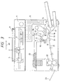
A perspective view of a digital copying
apparatus, embodying the present invention is shown in
Figure 2. The copying apparatus shown in Figure
2 comprises a reader A for reading original images
and a printer B for producing the images read by
the reader A on paper or other recording medium.
The reader A is equipped with an operation unit
A1 to be described later.
Figure 3 shows a cross section of the digital
copying apparatus shown in Figure 2. In conjunction
with Figure 2, the copying apparatus will be described
briefly.
An original is placed on an original glass
base 3 with the surface (original side), on which
images to be read are formed, facing down, then
pressed to the glass base 3 by an original cover
4. The original side is illuminated by a fluorescent
lamp 2. The reflected light is converged on the
face of a CCD sensor 1 or a reading sensor via
mirrors 5 and 7 and a lens 6. The mirrors 7 and
5 are moved in subscanning direction at relative
speeds of 2 : 1 so that the optical path from the
fluorescent lamp 2 to the CCD 1 will remain invariant.
Ar denotes an arrow indicating the subscanning
direction.
The reader A processes image signals in
series for each bit of the CCD sensor 1, then inputs
it to a laser scan optical unit 25 in the printer
B. The unit 25 consists of a semiconducting laser
unit, a collimator lens, a rotary polygon mirror,
an F- lens, and a corrective optical system.
Specifically, the image signal sent from the reader
A is fed to the semiconducting laser unit. There,
electricity is transferred into light. Then, the
light is emitted to the quickly rotating polygon
mirror via the collimator lens. The reflected light
travels to a photosensitive drum 8 and scans it.
Arranged in the process succeeding to the
photosensitive drum 8 are components for image
formation; such as, a predischarger 9, a pre-discharge
lamp 10, a primary charger 11, a secondary charger
12, a pre-exposure lamp 13, a developing unit 14,
a paper feed cassette 15, a feed roller 16, a feed
guide 17, resist rollers 18, a transfer charger
19, a separation roller 20, a transport guide 21,
fusing rollers 22, and a tray 23. A so-called laser
beam printer is employed as the printer B. An ink-jet
printer will also do.
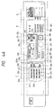
Figures 4A to 4D show the operation unit
of the copying apparatus shown in Figure 2. The
components will be described below. Figures 4B,
4C, and 4D are enlarged views of portions C, D,
and E in Figure 4A.
201 denotes a ten-key pad, which is used
to enter numeric values ranging from 0 to 9 in order
to specify the number of copies or a magnifying
power for zooming. 202 is a liquid crystal color
display panel or a touch panel, representing a color
screen display (designation means) for setting copy
modes or informing operators of operation procedures,
machine states, form sizes, and magnifying powers
for enlargement copy. 203 denotes a Reset key or
a key for initializing a currently specified mode.
204 is a Clear/Stop key, which stops an operation
when the machine is actuated, and clears the number
of copies or other numeric value specified with
a ten-key pad when the machine is not actuated.
205 denotes a Copy Start key for starting a copy
operation. 206 is a key for selecting a form size.
A selected form size, for example A4 appears on
a display panel 202. 207 denotes density adjustment
keys for adjusting copy density from the lightest
to darkest or vice versa. 208 represents nine light
emitting diodes (hereafter, LED) for indicating
a current density level. 209 is an original type
mode select key for selecting a character mode,
photography mode, or character/photography mode
according to the original type. 210 represents
LEDs each of which lights to indicate that the
character mode, photography mode, or character/photography
mode has been selected.
211 represents control keys including an
OK key 212, an Up arrow key 213, a Down arrow key
214, a Right arrow key 215, and a Left arrow key
216. The control keys are used to move a cursor
on the display panel 202 specify modes. 217 denotes
a rotary knob, which will be described in detail.
219 represents enlargement, reduction, and full-scale
keys for enlarging or reducing a regular form
size to another regular form size, or copying original
in full-scale. 220 is a Centering key for centering
an original in a copy form. When centering is
specified, an LED 220a lights. 221 is a Zoom key
for specifying a magnifying power in 1 % steps in
the range of 25 % to 400 %. 222 denotes a Longitudinal/Lateral
Independent Zoom key, which is used to
produce copies by changing the magnifying powers
for the longitudinal and lateral directions of
original in 1 % steps in the range of 25 % to 400 %.
223 is an Auto Zoom key, which is used to produce
copies automatically according to the size of an
original. 224 denotes a Binding Margin key for
moving an image of an original laterally to create
binding margins. 225 denotes an Area Designation
key for designating an area under an editor or other
area designation means. 226 or a Filter key is
used to adjust balance finely. 227 denotes a
Partial Processing key for specifying an operation
for a specific area or marker. 228 is a Pattern
key, which will be described in detail.
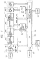
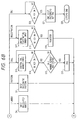
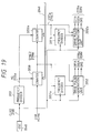
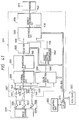
Figure 1 is a block diagram showing an
embodiment of the present invention, schematizing
a color patterning system for a copying apparatus
shown in Figures 2 and 3.
In Figure 1, color information of an original
300 passes through a lens 301a and a CCD sensor
301b in an image read unit 301, then enters an A/D
converter 301c to undergo A/D conversion. The
digitized signal goes to an image processing unit
302. In the image processing unit 302, a shading
correction circuit 302a performs shading correction
on the signal. Then, the signal advances to a color
recognition circuit 302b (color identification means).
In this stage, a color designated by a color patterning
control circuit 304 and a pattern designated according
to the color are recognized. Then, the signal advances
to a patterning circuit (conversion means) 302c.
The circuit 302c converts an area containing the
identified color into a corresponding pattern.
Then, the signal goes to an optical density conversion
circuit 302d and an image editing unit 302e. After
undergoing all operations in the image processing
unit 302, the signal advances to an image record
unit 303. The image record unit 303 includes a
control circuit for controlling a motor for transporting
transferred paper, a laser recording circuit for
writing video signals sent from the image processing
unit 302 on a photosensitive drum, and a developing
control circuit for developing. A CPU circuit 305
consists of a ROM 305a, a RAM 305b, and a CPU 305c,
which controls the image read unit 301, the image
processing unit 302, the image record unit 303,
a data processing circuit 306, an operation unit
A1, a digitizer 307, and an IC card 308, and thereby
globally handles sequence control of the copying
apparatus.
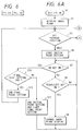
Figure 5 shows a screen for designating
color patterns displayed on a color screen display
202. When a Pattern key 228 is pressed, the liquid
crystal screen of the display 202 becomes as shown
in Figure 5 (steps S1 and S2 in Figure 6).
In Figure 5, 401 denotes a color plane
in which reference colors of red, blue, and green
appear. The reference colors are interposed with
intermediate colors. 402 indicates a field for
entering a patterning designation number (number
used for memory read to be described later). A
triangle cursor is moved to the Designation Number
field 402 using Up and Down keys 213 and 214 (step
S3). A designation number is entered using a
ten-key pad 201 or Left and Right keys 215 and 216
(see (a) of Figure 9A) (step S4). 403 indicates
a Designation Pattern field. The cursor is set
at the Designation Pattern using the Up and Down
keys 213 and 214 (step S3). The Left and Right
keys 215 and 216 are used to select a pattern (see
(b) of Figure 9A) (step S5).
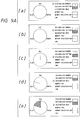
404 indicates a Designation Area field.
When the cursor is placed at the Designation Area
404 (step S3), a designated pattern (initially,
a line) appears in the color plane 401 (See (c)
of Figure 9A) (step S6). First of all, the Left
and Right keys 215 and 216 are used to move a line
(indicating a radius) to the position of a color
to be converted (See (d) of Figure 9A) (steps S7
to S9). An OK key 212 is used to determine an
initial point (See (c) of Figure 9A) (steps S7 to
S10). Then, the Left and Right keys 215 and 216
are used to move the designated pattern to another
position (terminal point) (See (a) of Figure 9B)
(steps S11, and S7 to S9). When the OK key 212
is pressed, an area between the initial and terminal
points (for example, an area between purple and
orange) is specified to be converted into the
designated pattern (See (b) of Figure 9B) (steps
S7, S10, and S12).
405 indicates a field of Memory Call for
reading the contents of a registration number
registered in a memory (RAM) 305b (See (c) of Figure
9B). Memory read is performed according to steps
S13 to S16 in Figure 6. The Up and Down keys 213
and 214 are used to set the triangle cursor at the
Memory Call (step S3). A registration number to
be called is entered, then the OK key is pressed
(steps S13 and S14). If the number has already
been registered, the contents of the registration
number are read (steps S15 and S16). After that,
control is returned to the step S3.
406 indicates a field of Memory Registration
for placing a designated area and pattern in the
memory 305b together with a registration number
(See (d) of Figure 9B). Memory registration is
performed according to steps S17 to S19 in Figure
6. The Up and Down keys 213 and 214 are used to
set the triangle cursor at the Memory Registration
(step S3). A registration number is entered and
the OK key 212 is pressed (steps S17 and S18).
Thus, the designated area and pattern are registered
(step S19).
407 indicates an End field for termination,
which is used to return the display 202 to the
reference screen. Termination is performed according
to steps S20 to S22 in Figure 6. The Up and Down
keys 213 and 214 are used to set the triangle cursor
at the End (step S3). When the OK key 212 is pressed
(step S20), color patterning setting terminates
(step S21). Then, the display 202 returns to the
reference screen (See (e) of Figure 9B) (step S22).
An indicator 408 indicates a memory number
(registration number) to be registered. When the
OK key 212 is turned on (step S18), the memory number
is registered. If a memory number to be registered
has already been registered, the indicator 498 blinks
the number. When the indicator 498 is blinking,
if the OK key 212 is turned on, new contents are
overwritten on the contents already registered.
An indicator 409 indicates a registration
number to be called. When the OK key 212 is turned
on (step S14), the registration number is called.
If a called registration number has not been registered,
the indicator 409 blinks the number. At this time,
calling is not done.
Next, other embodiment of the present invention
will be described in conjunction with Figures 4
and 6 described above as well as Figures 7, 10A
and 10B.
In the foregoing embodiment, an area is
converted into a color pattern using a color plane
on a color screen 202 of an operation unit, or
specifically, Left and Right keys 215 and 216 are
used to move the color pattern to designate the
area. In this embodiment, the color plane is moved
to specify a color pattern.
Figure 7 shows an image for designating
a color pattern displayed on the color screen display
202. When a Pattern key 228 is pressed, the screen
202 or a liquid crystal screen becomes as shown
in Figure 7. 601 and 610 represent color planes.
602 denotes a patterning Designation Number field.
A triangle cursor is set at the Designation Number
using Up and Down keys 213 and 124 (step S3 in Figure
6). A ten-key pad 201 or the Left and Right keys
215 and 216 are used to enter a designation number
(See (a) of Figure 10A) (step S4). 603 denotes
a Designation Pattern field. The cursor is set
at the Designation Pattern 603 using the Up and
Down keys 213 and 214. The Left and Right keys
215 and 216 are used to select a pattern (See (b)
of Figure 10A) (step S5).
604 denotes a Designation Area filed. When
the cursor is set at the Designation Area 604, a
designated pattern (initially, a line) appears in
the color plane 610. This line extends from the
center point of the color plane 610 to the circumference
of a smaller circle or toward the mark
or a position P1 (a position P2 is on the opposite
side of P1) (See (c) of Figure 10A) (step S6).
The Left and Right keys 215 and 216 are used to
rotate the color plane 610, and thus move the line
to the position of an intended color (See (d) of
Figure 10A) (steps S7 to S9). In this embodiment,
the color plane 610 is rotated counterclockwise
when viewed from above the drawing, as shown in (d)
of Figure 10A. Then, an OK key 212 is used to
determine an initial point (See (e) of Figure 10A)
(steps S7 and S10). The Left and Right keys 215
and 216 are used to rotate the color planes 601
and 610 together with the designated pattern to
other position (terminal point) (See (a) of Figure
10B) (steps S11, and S7 to S9). When the OK key
212 is pressed, the area between the initial and
terminal points is specified to be converted into
the designated pattern (See (b) of Figure 10B) (steps
S7, S10, and S12).
Symbols 605 to 609 in Figure 7 correspond
to 405 to 409 in Figure 5. The operations are the
same. The description will, therefore, be omitted.
Next, other embodiment of the present
invention will be described in conjunction with
Figure 8.
In the aforesaid embodiment, an area is
converted into a color pattern using a color plane
on a color screen of an operation unit, or
specifically, Left and Right keys 215 and 216 are
used to move the color plane or a pattern to
designate the area and pattern. In this embodiment,
a rotary knob 217 (Figure 4) having a color plane
is used to specify a color pattern. On the screen
shown in Figure 5 or 7, a color range for a pattern
is specified using the Left and Right keys 215 and
216. In this embodiment, the rotary knob 217 having
the color plane is employed. The knob 217 operates
in synchronization with the color plane on the color
screen. When the knob 217 is rotated, the color
plane on the screen rotates.
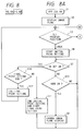
Figure 8 is a flowchart showing the setting
operation. Figure 8 differs from Figure 6 in a
point that a step S23 comes instead of a step S8,
or that the knob 217 is used instead of the Left
and Right keys 215 and 216. As described previously,
the functions of the knob 217 are identical to those
of the Left and Right keys 215 and 216. The
description will, therefore, be omitted.
Thus, the aforesaid embodiments of the present
invention do not require area designation and point
designation using a digitizer which are indispensable
to copying apparatuses of prior art. Color patterning
can be executed merely by designating a color plane
with a pattern. This results in ease of operation
and speedy processing.
Color patterning can be finely adjusted
effortlessly.
Other embodiment of the present invention
will be described in conjunction with Figures 11
to 14.
Figure 11 is a side view showing the
internal configuration of an image processing
apparatus of an embodiment of the present invention.
2001 denotes an original feeder. Originals stacked
on the original feeder are sequentially carried
onto an original glass base one by one. When an
original is carried, a lamp on a scanner 2004 of
a scanner unit 2003 lights. Then, the scanner unit
2003 moves to emit light all over the original.
Light reflected from the original passes
through a lens 2008 via mirrors 2005, 2006, and
2007, then enters a color CCD image sensor 2009
in a reader 2009. An image signal fed to the color
CCD image sensor 2009 or an input signal sent from
the reader 2009 shown in Figure 12 is processed
by an image signal control circuit 2011 under the
control of a CPU 2010, then fed to a printer 2012.
The signal fed to the printer 2012 is
converted into an optical signal by an exposure
control 2013 shown in Figure 11. Thus, light is
emitted over a photosensitive drum 2014 according
to the image signal. The light emitted creates
a latent image on the photosensitive drum 2014.
Then, the latent image is developed by a primary
developing unit 2015 or a secondary developing unit
2016.
When the latent image is created, a transferred
form is fed from a primary transferred form stacker
2017 or a secondary transferred form stacker 2018
at the same time. Then, the developed image is
transferred onto the transferred form.
Then, the transferred image is fused on
the transferred form by fusing rollers 2020. After
that, the transferred form is ejected from the
apparatus by ejecting rollers 2021. 2022 in Figure
12 denotes an operation unit, and 2023, ROM, RAM,
or any other storage element.
(Normal copy mode)
Next, the operation of an image processing
apparatus according to the present invention in
normal copy mode will be described in conjunction
with Figure 13.
Image information of R (red), G (green),
and B (blue) signals, which have been photoelectrically
transferred from an original by a color CCD image
sensor 2009a in a reader 2009, go to amplifiers
2024, 2025, and 2026 corresponding to the three
colors. These amplifiers 2024, 2025, and 2026
amplify the R, G, and B signals to the input levels
of A/ D converters 2027, 2028, and 2029 in an image
signal control circuit 2011. Then, the amplified
R, G, and B signals 1010, 1020, and 1030 enter the
A/ D converters 2027, 2028, and 2029. These A/ D
converters 2027, 2028, and 2029 convert the R, G,
and B signals 1010, 1020, and 1030 of analog image
information into digital signals 1040, 1050, and
1060. The output (digital) signals 1040, 1050,
and 1060 of the A/ D converters 2027, 2028, and 2029
enter a Y signal generation circuit 2030 in the
next stage to produce a luminance signal Y according
to the following expression:
Y = 0.30R + 0.59G + 0.11B
where, R represents a signal 1040, G, a signal 1050,
and B, a signal 1060.
The multivalued luminance signal Y is fed
to a binarization circuit 2031 in the next stage
and converted into a binary luminance signal 1085.
The binary luminance signal 1035 enters a selector
2032 to become a binary-coded signal 1090. The
binary-coded signal 1090 goes to a synthesis circuit
2033 in the next stage. The selector 2032 selects
the binary luminance signal 1085 under the control
of a CPU 2010. The synthesis circuit 2033 changes
its functions under the control of the CPU 2010,
and selects only the signal 1090 in normal copy
mode.
An output signal 1130 of the synthesis circuit
2033 goes to a density conversion circuit 2034 in
the next stage. The density conversion circuit
2034 has a function for providing a printer 2012
with a signal 1140 generated by reversing the
polarity of a composite signal 1130 sent from the
synthesis circuit 2033. The output signal 1140
of the density conversion circuit 2034 enters a
printer 2012 in the next stage to form a monochrome
image.
(Color detection composite mode)
Next, the operation of an image processing
apparatus in color detection composite (synthesis)
mode will be described in conjunction with Figures
12 to 14.
In the color detection composite mode,
characters representing the names of colors are
printed on a monochrome output image according to
the color information in an original. This helps
discern color areas of an image.
Before executing a copy operation, the color
detection composite mode is specified at an operation
unit 2022 shown in Figure 12. When a Start key
on the operation unit 2022 is pressed, a copy
operation starts. Image information containing
color information of R, G, and B signals 1010, 1020,
and 1030 are read from an original by a color CCD
image sensor 2009a in a reader 2009, then, as described
concerning the normal copy mode, converted into
digital signals 1040, 1050, and 1060 by A/D
converters 2027 to 2029. Then, the digital signals
are recomposed by a Y signal generation circuit
to produce a luminance signal Y. The luminance
signal Y is changed to a binary luminance signal
1085 by a binary coding circuit 2031 in the next
stage. Then, the binary luminance signal 1085
becomes a binary-coded signal 1090 after passing
through a selector 3032 in the next stage.
On the other hand, the R, G, and B signals
1040, 1050, and 1060 sent from the A/ D converters
2027, 2028, and 2029 enter a color detection circuit
2035 as well as the Y signal generation circuit
2030. The combinations of level ratios of the R,
G, and B signals 1040, 1050, and 1060 are compared
with a preprogrammed color detection table to detect
the colors contained in an input signal. At the
same time, the color detection circuit 2035 identifies
areas having the same colors and sends an identification
signal (color detection signal) 1080 to a character
pattern generator 2036. The character pattern
generator 2036 generates character patterns indicating
the color names informed with the detection signal
1080 sent from the color detection circuit 2035.
The character pattern generator 2036 provides the
synthesis circuit 2033 with a character pattern
signal.
The synthesis circuit 2033 synthesizes the
binary-coded signal 1090 sent from the aforesaid
binarization circuit 2031 and the character pattern
signal 1110 sent from the character pattern generator
2036, then inputs the resultant signal to the density
conversion circuit 2034 in the next stage. With
the indentification signal 1080 sent from the color
detection circuit 2035, the binary-coded signal
1090 in which color information contained in the
binary luminance signal 1085 from the binarization
circuit 2031 is converted into white information
by the selector 2032 is sent to the synthesis circuit
2033. The density conversion circuit 2034 outputs
a signal 1140 generated by reversing the polarity
of a composite signal 1130 of the binary-coded signal
1090 and character pattern signal 1110. The output
signal of the density conversion circuit 2034 goes
to a printer 2012 in the next stage to produce a
monotone or monochrome image with character patterns
representing color names appended.
The effects of the aforesaid image processing
apparatus in color detection composite mode will
be described in conjunction with Figures 14 and
15.
2037 in Figure 14 denotes a colored original.
2038 in Figure 15 is an image the image processing
apparatus has printed after reading the colored
oritinal 2037 and processing the read data.
The original 2037 shown in Figure 14 is
a bar chart indicating the numbers of patent
applications by laboratories A, B, and C for
comparison study. A bar graph A1 for the laboratory
A is colored with red, a bar B1 for the laboratory
B, with blue, and a bar C1 for the laboratory C,
with green. Figure 15 shows a processed image 2038
the image processing apparatus has produced using
the original 2037. In the monochrome or monotone
processed image 2038, character patterns representing
characters "RED", "BLUE", and "GREEN" indicating
the names of the colors of the bar graphs A1, B1,
and C1 in the original 2037 of Figure 14 are
synthesized on the bar graphs A1, B1, and C1 shown
in Figure 15. This makes it possible to recognize
the colors of pixels in the color images of the
original 2037.
As described above, the colors in the original
images are detected using color information an
information generation means has generated, then
character patterns indicating the color names are
generated according to the color detection signal.
Therefore, even if a low-priced monochrome printer
is employed, it is possible to provide monotone
processed images which permits effortless and
accurate recognition of the colors of pixels in
original images.
Next, other embodiment of the present
invention will be described in conjunction with
Figures 16 to 33.
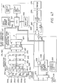
Figure 16 is a block diagram of an image
processing apparatus according to other embodiment
of the present invention. A fully-colored original
is exposed to light originating from an exposure
light which is not shown. The reflected color image
is formed by a color image is formed by a color
CCD image sensor. The provided analog image signal
is digitized by an A/D converter. The fully-colored
digital image signal is processed, filtered, then
fed to a thermal transfer printer, ink-jet printer,
or laser beam printer, which is not shown. Thus,
an image is produced.
An original is illuminated by an exposure
lamp which is not shown. The reflected light is
handled by a color CCD image sensor 2040 in a reader
2040 so that colors will be separated for each image.
Then, the read color signals are amplified to given
levels by amplifiers 2041-1, 2041-2, 2041-3, 2041-4,
and 2041-5. In this cofiguration, the color CCD
image sensor 2040a is driven by CCD driver 2042.
Figure 17 is a configuration diagram of
the color CCD image sensor 2040a shown in Figure
16.
The color CCD image sensor 2040a used in
this embodiment is designed to read an image signal
as five different portions arranged in main-scan
direction. Herein, one pixel is assumed to be
63.5 µm long. The color CCD image sensor 2040a
supports 400 dots per inch (hereafter, dpi) and
permits 1024 pixels. One pixel falls into color
components G, B, and R arranged in main-scan
direction as shown in Figure 17. Consequently,
the color CCD image sensor 2040a provides a total
of 3072 (1024 x 3) effective pixels.
On the other hand, chips 2043a, 2044a, 2045a,
2046a, and 2047a of the color CCD image sensor 2040a
are formed on the same ceramic substrate. The first,
third, and fifth chips 2043a, 2045a, and 2047a are
arranged on the same line LA, and the second and
fourth chips 2044a and 2046a, on a line LB at a
distance of four lines or 254 µm (63.5 µm x 4) from
the line LA. An original is scanned and read in
A1-arrow direction.
Figure 18 is a timing chart showing an
example of timings of drive pulses shown in Figure 17.
Among the five chips 2043a, 2044a, 2045a,
2046a, and 2047a in the color CCD image sensor 2040a,
the first, third, and fifth chips 2043a, 2045a,
and 2047a are driven independently and synchronously
with a sensor drive pulse ODRV 2118A, and the second
and fourth chips 2044a and 2046a, with an EDRV 2119A.
O01A, O02A, and ORS contained in the ODRV 2118a,
and EO1a, E02A, and ERS contained in the EDRV 2219a
serve as charge transfer clocks and charge reset
pulses respectively for chips. The charge transfer
clocks and charge reset pulses are generated to
be fully synchronous, so that they will not jitter
mutually. This suppresses mutual intervention
between the first, third, and fifth chips 2043a,
2045a, and 2047a, and the second and fourth chips
2044a and 2046a, or minimizes noise. From this
viewpoint, the pulses are generated by a single
reference oscillation source OSC 2048 (See Figure
19).
Figure 19 is a block diagram of the CCD
driver 2042 shown in Figure 16, and Figure 20, a
timing chart showing an example of timings of
components shown in Figure 19.
In Figure 19, a raw clock CLKO 2138 the
signal reference oscillation source OSC 2048
generates is frequency-divided by a first frequency
divider 2051 to produce a clock KO 2135a. The clock
KO 2135a generates reference signals SYNC2 and SYNC3
for determining timings of generating the ODRV 2118a
and EDRV 2119a. Timings of outputting the reference
signals SYNC2 and SYNC3 are determined according
to the set values of presettable counters 2050
and 2050a which are specified via a signal cable
2049 linked to a CPU bus. The reference signals
SYNC2 and SYNC3 initialize second and third frequency
dividers 2051a and 2051b as well as drive pulse
generation circuits 2052 and 2052a.
Specifically, with input of a scan reference
signal HSYNC 2118, the sensor drive pulses ODRV
2118a and EDRV 2119a are generated according to
the raw clock CLKO 2138 sent from the single reference
oscillation source OSC 2048 and the frequency-division
clock KO 2135a generated in synchronization with
the raw clock CLKO 2138. Therefore, the sensor
drive pulses ODRV 2118a and EDRV 2119a are provided
as fully synchronous signals without a jitter.
This prevents signal distortion due to mutual
intervention among chips.
The sensor drive pulse ODRV 2118a or one
of sensor drive pulses which are mutually synchronous
is fed to the first, third, and fifth chips 2043a,
2045a, and 2047a shown in Figure 17. Other sensor
drive pulse EDRV 2119a is fed to the second and
fourth chips 2044a and 2046a. The chips 2043a,
2044a, 2045a, 2046a, and 2047a independently provide
image signals V1, V2, V3, V4, and V5 in synchronization
with drive pulses. The image signals are amplified
to given voltage levels by amplifiers 2041-1 to
2041-5 independently installed in channels CH1,
CH2, CH3, CH4, and CH5 shown in Figure 16. Then,
the image signals V1, V3, and V5 are transmitted
via a coaxial cable 2053 according to the timing
of OOS 2129 shown in Figure 18, and the image signals
V2 and V4, according to the timing of EOS 2134.
Eventually, the image signals go to an image signal
processing circuit.
Image information of an original is fed
to the image signal processing circuit, then read
as five different portions of color image signals.
The color image signal is decomposed into G, B,
and R signals of green, blue, and red by a sample-and-hold
(hereafter, S/H) circuit 2054 shown in
Figure 16. Namely, the S/H circuit 2054 outputs
signals of 15 (3 x 5) channels.
Analog color image signals sent through
the channels 1 to 5 CH1 to CH5, whose R, G, and
B color components are sampled and held by the S/H
circuit 2054, are digitized by an A/D conversion
circuit 2055 in channels. The digitized signals
originating from the channels 1 to 5 CH1 to CH5,
which are mutually independent and lined in parallel,
go to an aberration correction circuit 2056.
In this embodiment, as described previously
(See Figure 17), the color CCD image sensor 2040a
in the reader 2040 has a width of four lines or
245 µm (63.5 µm x 4) in sub-scan direction and falls
into five areas in main-scan direction. Thus, this
sensor has a staggered structure of five components
for reading originals. Therefore, an aberration
is created between the reading position of the
channels 2 and 4 CH2 and CH4, which are leading
in scanning, and that of the remaining channels
1, 3, and 5 CH1, CH3, and CH5. Then, the aberration
correction circuit 2056 having a memory for storing
data of multiple lines is used to correct the
aberration. Thus, coherent information is transmitted
through the five channels.
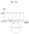
Figure 21 is a block diagram of a black
correction circuit of a black correction/white
correction circuit 2057 shown in Figure 16.
Black-level outputs of channels 1 to 5 CH1
to CH5 vary greatly among chips 2043a to 2047a or
pixels, as shown in Figure 22, when the quantity
of incident light of a color CCD image sensor 2040a
is very small. If the outputs are fed to a printer
2102 as they are, image data will contain streaks
or become non-uniform.
The variations among output black levels
must be corrected. For this correction, a circuit
shown in Figure 21 is employed for the correction.
Prior art reading an original, an original
scan unit is moved to a black plate having uniform
density which is arranged in a non-imaging area
at the distal end of an original base, an exposure
lamp is lit, then a black level image signal is
fed to the black correction circuit of the black
correction/white correction circuit 2057.
First, consideration is taken into a B signal
Bin. To store the image data for one line in a
black level RAM 2058, a first selector 2059 must
select A (control line d), a gate 2060 must close
(control line a), then other gate 2061 must open
(control line b). That is to say, signal lines
2062, 2063, and 2064 are connected in that order.
On the other hand, an address input signal line
2065 of the black level RAM 2058 must be initialized
with a scan reference signal HSYNC and provided
with an output signal 2067 of an address counter
2066 for counting pixel clocks VCLK. Therefore,
a signal for a second selector 2068 is fed over
a control signal line c. Thus, a black level signal
for one line is stored in the black level RAM 2058
(a mode in which the foregoing operation is performed
is referred to as a black reference value fetch
mode).
During image read, the black level RAM 2958
is placed in data read mode. An image is read pixel
by pixel and fed to an input B of a subtracter 2070
by tracing the lines in the route from the signal
lines 2064 through 2069. That is to say, the gate
2061 closes (control line b), while the gate 2060
opens (control line a). A third selector 2071 selects
an output A.
Therefore, a blcak correction circuit output
signal 2157 from the subtracter 2070 is controlled
with a signal 2072B, and provided as Bin (i) - DK (i) =
BOUT (i), wherein a blue signal Bin is an input
and black level data is represented as DK (i) (a
mode in which this operation is performed is referred
to as a black correction mode).
Similarly, when it comes to a G signal Gin
and an R signal Rin, control is passed with signals
2072G and 2072R. The states of the control lines
a, b, c, d, and e of the selectors 2059, 2068, and
2071, and the gates 2060 and 2061, which are used
for the control, are changed by a latch 2074 allocated
as an input/output of a CPU 2073 (See Figure 27)
under the control of the CPU.
When the selectors 2059, 2068, and 2071
select the Bs, the CPU 2073 can access the black
level RAM 2058.
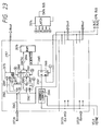
Figure 23 is a block diagram of a white
correction circuit of the black correction/white
correction circuit 2057 shown in Figure 16.
During white level correction (shading
correction), sensitivity variations of an illumination
system, an optical system, and a sensor are corrected
based on white data obtained by illuminating an
original scan unit with a uniform white plate moved.
The basic circuit configuration of the white
correction circuit is identical to that of the black
correction circuit shown in Figure 21. Only one
difference is that a subtracter 2070 is employed
for black correction but a multiplier 2075 is employed
for white correction. The same components will
be assigned the same symbols. The description will,
therefore, be omitted.
In color correction, when a color CCD image
sensor 2040a for reading originals is at a read
(home) position of a uniform white plate, or when
a copy operation or read operation has not been
performed, an exposure lamp which is not shown is
lit and image data of uniform white level for one
line is stored in a correction RAM 2076.
For example, when an A4 form is placed with
its longitudinal length in main-scan direction,
the correction RAM 2976 supporting 400 dpi needs
a capacity of at least 4677 bytes for 4677 pixels
(297 mm divided by 0.0635 mm). As shown in Figure
24, assuming that white plate data at the i-th pixel
is Wi (i = 1 to 4677), data acquired from the white
plate is stored for each pixel in the correction
RAM 2076 as shown in Figure 25.
On the other hand, assuming that white plate
data is Wi and a read value of the i-th pixel of
a normal image is Di, corrected data Do should be
represented as Do = Di x FFH/Wi. Therefore, a CPU
2073 controls a latch 2074 to provide outputs to
control lines a, b, c, d, and e, so that gates 2060
and 2061 will open and first to third selectors
2059, 2068, and 2071 will select Bs. Thus, the
CPU 2073 can access the correction RAM 2076.
Next, the CPU 2073 calculates FFH/Wo for
the leading pixel Wo, FFH/Wi for Wi, etc. sequentially
according to the control sequence shown in the
flowchart of Figure 26, then replaces data.
Specifically, when i is initialized to 0 (step S101),
Wi is read (step S102) and calculated (step S103).
When the Wi is written in the RAM 2076 (step S104),
i is incremented by 1. The sequence from S102 to
S105 is repeated until i becomes 2673 (step S106).
When i becomes 4673 at the step S106, a process
for a blue component B is completed. Next, a green
component G and a red component R are handled similarly.
After that, the gate 2060 (control line a) in Figure
23 is opened and the other gate 2061 (control line
b) is closed, so that Do (Di x FFH/Wi) will be
provided for an input of raw image data Di. Thereby,
the second and third selectors 2068 and 2071 select
As. Coefficient data FFH/Wi read from the correction
RAM 2076 is routed through signal lines 2064 to
2069, then multiplied by raw image data sent over
a signal line 2062. Finally, the product is provided
as an output.
As described above, black and white levels
are corrected by correcting various factors including
the variations in black level sensitivity of an
image input system, in dark current of the color
CCD image sensor 2040a, in sensitivity among the
chips 2043a to 2047a, in the quantity of light
of an optical system, and in white level sensitivity.
Thus, image data Bout 2121, Gout 2122, and Rout
2123 in which white and black levels of each color
are corrected to be uniform are provided in main-scan
direction.
Image data made up of 8-bit color components
R, G, and B, in which white and black levels have
thus been corrected, is fed to a luminance (Y) signal
generation circuit 2077 and a color detection circuit
(color detection means) 2078 shown in Figure 16.
First, the luminance signal generation circuit
2077 will be described.
The luminance signal generation circuit
2077 processes an image signal, which has been read
by a color CCD image sensor 2040a and undergone
color separation, to generate a monochrome image
signal. The generated monochrome image signal
includes colors unseparated and has its highest
wavelength. This is because that a printer or an
image formation means of this embodiment has only
a monochrome or monotone image formation function.
The luminance signal generation circuit 2077 performs
an operation according to the following formula:
Dataout = (R + G + B) /3
Namely, input data of color components R, G, and
B is averaged. In this embodiment, an adder and
a multiplier are employed. A calculated luminance
signal Y is fed to a selector 2087 which will be
described later.
Figure 27 is a block diagram of a color
detection circuit 2078 shown in Figure 16.
Input data of a luminance signal generation
circuit 2077 is also an input of the color detection
circuit 2078. In this embodiment, a hue signal
is used to detect a color. This is because a single
color may vary in luminance and brightness. Using
hues as a determinant, colors can be identified
correctly.
First, a color detection procedure will
be described briefly.
Each of R, G, and B color data consists
of eight bits. Therefore, an input of R, G, and
B color data contains information of a total of
224 colors. To use this abundant information as
it is, a large-scale circuit is needed, costing
very high.
Therefore, this embodiment deals with
aforesaid hues which differ from normally-understood
"hues" to be exact. However, a term "hue" is employed
here. It is widely adopted that a color space known
as a Munsell's cube is designated with saturations,
luminosities, and hues.
Each of R, G, and B color data must be
converted into plane or two-dimensional data. A
common component of the R, G, and B color data,
or a minimum value min (R, G, B) of the R, G, and
B color data is an achromatic color component.
Based on this fact, the min (R, G, B) is subtracted
from each of R, G, and B data. Then, using the
remaining information as chromatic color components,
a three-dimensional input color space is converted
into a two-dimensional color space.
A converted plane is divided radially into
six portions as shown in Figure 28. Input information
or an order of sizes of color signals R, G, and
B; that is, R>G>B, R>B>G, G>B>R, G>R>B, B>G>R, or
B>R>G, and input of maximum and mean values of the
R, G, B signals are assessed in the light of a lookup
table to obtain a hue level.
Next, the operation of the color detection
circuit 2078 will be described in conjunction with
Figures 16 and 27.
Inputs of R, G, and B color data are fed
to a max/mid/min detection circuit 2079 shown in
Figure 27 for determining which data components
are the biggest and smallest. The max/mid/min
detection circuit 2079 uses a comparator to compare
each input data, then outputs maximum, mean, and
minimum values according to the result of comparison.
The output values of the comparator are provided
as an order signal.
As described previously, an achromatic color
component is subtracted from the maximum and mean
values. Therefore, subtracters 2080 and 2081 are
used to subtract the minimum value from the maximum
and mean values. Then, the subtracted values are
fed to the color hue detection circuit 2082 together
with the order signal.
The hue detection circuit 2082 is formed
with a RAM, ROM, or other randomly accessible storage
element. In this embodiment, a ROM is employed
to constitute the lookup table. The ROM contains
values corresponding to angles of the plane shown
in Figure 28 and provides a hue level depending
on an input order signal, (maximum - minimum) value,
and (mean - minimum) value.
An output hue level is fed to window
comparators 2083 and 2084. These window comparators
2083 and 2084 receive the hue levels of colors to
be patterned from a data input means which is not
shown. A CPU 2073 allocates specific offsets to
a hue level matching with a color, then specifies
the values with offsets in the window comparators
2083 and 2084. The window comparators are designed
so that assuming that a value specified in the window
comparator 2083 is a1, when a hue level is larger
than a1, the output will be "1", and assuming that
a value specified in the other window comparator
2084 is a2, when a hue value is smaller than a2,
the output will be "1".
Consequently, when the condition below is
met:
a1 < hue value < a2
an AND gate 2085 in the following stage sets "1"
which will be an output of the color detection
circuit 2078 shown in Figure 16.
When multiple sets of window comparators
are employed, multiple colors can be detected.
An identification signal resulting from
the identification by the color detection circuit
2078 enters the AND gate 2086 and selector 2087.
The AND gate 2086 performs gating on a character
pattern signal representing color names generated
from a character pattern generation circuit 88 to
be described later. The selector 2087 will be
described later.
Next, the character pattern generation
circuit 2088 and an address control circuit 2089
will be described in conjunction with Figure 29.
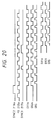
The character pattern generation circuit
2088 is formed with a character pattern ROM 2090
containing character pattern dot data. In the
character pattern ROM 2090, "1s" and "0s" are
written at addresses corresponding to superordinate
and subordinate addresses as shown in Figure 30.
A character pattern made up of this data is shown
in Figure 31.
As shown in Figure 29, a main-scan counter
2091 and a sub-scan counter 2092, which are
synchronous with a pixel clock VCLK and a scan
reference signal HSYNC respectively, generate
address signals for the character pattern ROM
2090. The address signals are fed to the character
pattern ROM 2090. Reference signals ITOP, HSYNC,
and VCLK are timing signals shown in Figure 32.
The ITOP signal indicates the top of an image, and
remains low while the color CCD image sensor 2040a
is reading image data.
The main-scan counter 2091 is synchronous
with the scan reference signal HSYNC and counts
pixel clocks VCLK. The sub-scan counter 2092 is
synchronous with the image top signal ITOP and
counts scan reference signals HSYNC to generate
addresses of the character pattern ROM 2090.
Depending on the identification result of
the color detection circuit shown in Figure 6, the
AND gate 2096 in Figure 16 performs gating on a
character pattern signal. Then, the character pattern
signal is multiplied by a min (R, G, B) image signal
by a multiplier 2093. The min (R, G, B) image
signal is a signal the color detection circuit 2078
generates, indicating a minimum (darkest) value
among input image signals in which color components
R, G, and B have been separated. This signal is
needed because a luminance signal generation
circuit 2077 generates differs in level
from color to color. For example, the signal level
for yellow is very close to that for white, causing
the image data in an original to be missing.
When the min (R, G, B) signal enters a
contour extraction circuit 2094, image contours
are extracted. A generally-known Laplacian filter
is used to extract image contours. Then, an adder
2095 adds an extracted image counter signal to the
min (R, G, B) signal which has passed through a
multiplier 2093 to fetch image data.
Specifically, the adder 2095 adds a counter
signal expressing the counter of a character image,
for example, A as shown in Figure 33A and a min
(R, G, B) signal expressing a character pattern
consisting of, for example, Rs as shown in Figure
33B, to be appended to color information. The min
(R, G, B) signal provides a character pattern, wherein
Rs each of which represents the name of the color
of a contoured character image A are distributed
all over the A character image. An output signal
of the adder 2095 enters a selector 2087 in the
next stage.
The selector 2087 provides an input A with
the aforesaid luminance signal and an input B with
the min (R, G, B) expressing a contoured image.
When the detection result sent from the color
detection circuit 2078 is 1, the input B is selected.
When it is 0, the input A is selected. Then, the
selected input is fed to a log (density) conversion
circuit 2096 for converting a luminance signal into
a density signal, and converted into a density signal.
Then, the density signal enters a printer 2102 to
provide a monotone image having a character pattern
or a countered character A consisting of multiple
Rs each of which indicates the name of the color
of the character.
Thus, a contour signal is added to an image
signal. Then, the image signal is mixed with a
character pattern signal containing color names
or color information to produce an image. This
results in a monochrome or monotone image which
makes it possible to discern the colors of pixels
in the color images of an original.
Namely, character patterns always appear
in areas of white background, which will never be
indiscernible.
Next, other embodiment of the present
invention will be described in conjunction with
Figures 34 to 36. This embodiment performs pre-scanning,
recognizes color information of an original,
converts the color information into graphic patterns,
and adds on color names for the graphic patterns
to any specified areas. This is only a difference
between this embodiment and the previous one. Other
components are identical to those of the previous
embodiment. The description will, therefore, be
omitted.
Figure 34 is a flowchart showing the sequence
of operations of the embodiment.
In Figure 34, key input is performed at
a step S111. At a step S112, it is identified whether
or not a Start key is turned on. If the Start key
is not turned on, control is returned to the previous
step S111. If it is turned on, control is advanced
to the next step S113. At the step S113, it is
identified whether color recognition image editing
has been selected. If the color recognition image
editing has been selected, pre-scanning is performed
to read image information from an original (step
S114). At the same time, a histogram is created
using the image information (step S115).
The histogram indicates frequencies of
hues as shown in Figure 35. That is to say, the
chart of Figure 35 implies that colors rating high
in frequency exist in many areas of an origianl.
In this embodiment, the first, second, and third
colors exist in an original.
Next, a color CCD image sensor 2040a reads
an image (step S116). At the next step S117, image
editing and adding on are executed. That is to
say, in consideration of information used for
creating the histogram at the step s115 and an
original 2097 in which three bar graphs are colored
with red, blue, and yellow as shown in Figure 36A,
graphic and character patterns are appended to the
upper right of a form so that the relationships
between graphic patterns and colors can be understood.
Then, the graphic patterns are added on to the bar
graphs. The resultant monochrome or monotone
processed image 2098 is printed by a printer.
If color recognition image editing is not
selected at the step S113, control is advanced to
the step S119, then a normal operation is performed.
Then, the resultant image is printed by a printer
at the step S118. The normal operation performed
at the step S119 is a normal image copy operation.
The graphic patterns make it possible to
recognize color differences at sight.
Next, other embodiment of the present
invention will be described in conjunction with
Figures 37 and 40. This embodiment does not perform
pre-scanning. This is only a difference from the
previous embodiment. Other components and operations
are identical to those of the previous embodiment.
The description will, therefore, be omitted.
In this embodiment, pre-scanning is not
performed, but a preprogrammed collation table for
collating character patterns representing color
names with graphic patterns is printed independently
of a monotone image. Figure 37 is a flowchart
showing the sequence of operations in this embodiment.
At a step S121 in Figure 37, key input is
performed. At the next step S122, it is identified
whether or not a Start key is turned on. When the
Start key is turned on, control is advanced to the
next step S123. At the step S123, it is identified
whether or not color recognition image editing has
been selected. If color recognition image editing
has been selected, data indicating the relationships
between graphic patterns and colors is generated.
At the next step S125, based on an original 2099
showing an image in which three bar graphs are
colored with red, blue, and yellow as shown in
Figure 38, a collation table consisting or graphic
patterns indicating their relationships with colors
and character patterns representing color names
is produced as shown in Figure 39.
After the collation table is produced at
the step S125, the original is scanned to read image
information at the next step S126. At the next
step S127, color recognition and image editing are
performed under preprogrammed hue conditions. Then,
a monotone processed image 2101 in which graphic
patterns are added on to the bar graphs is fed from
a printer (step S128). Unless color recognition
image editing is selected at the step S123, normal
processing is done at a step S129. Then, a monotone
processed image 2101 is produced at a step S128.
In this embodiment, a graphic pattern generation
means may be installed in addition to a character
pattern generation means. Alternatively, a graphic
pattern generation function may be implemented in
the character pattern generation means.
Thereby, only graphic patterns are added
on to an output monotone processed image, but
character patterns are not. This eliminates a
feeling of incompatibility between original and
output monotone processed images.
A reader is employed as an information
generation means. However, this embodiment is also
applicable to outputs of a computer or VTR.
Furthermore, an output unit is not confined to a
printer but may, needless to say, be a monochrome
display or a facsimile.
Other embodiment of the present invention
will be described. An image processing apparatus
according to the embodiment converts color information
of an original to graphic patterns and registers
any graphic patterns.
(Pattern registration mode)
The operation of an image processing
apparatus in pattern registration mode will be
described in conjunction with Figures 11, 12, 41,
42, and 43.
The pattern registration mode comes before
a color detection pattern mode to be described later,
wherein desired patterns are registered for specific
colors with the image processing apparatus.
An operation unit 2022 arranged in the front
of an original base 2002 as shown in Figure 42 is
used to specify the pattern generation mode. The
operation unit 2022 includes a display section 3035
and an input section 3036.
The display section 3035 is formed with
a liquid crystal display, which shows, for example,
various graphic patterns to be specified for the
first to ninth colors; such as, a lateral stripe
pattern 30371, a leftward tilting line pattern
30372, a rightward tilting line pattern 30373, a
vertical stripe pattern 30374, a vertical waveform
pattern 30375, a lateral waveform pattern 30376,
a multi-dot pattern 30377, a sawtooth pattern made
up of multiple small triangles 30378, and a polka
dot pattern made up of multiple small circles 30379.
The input section 3036 includes 0 to 9 numeric keys
(ten-key pad) 30360, 30361, 30362, 30363, 30364,
30365, 30366, 30367, 30368, and 30369, a Pattern
Registration key 303610, a Start key 303611, and
a Color Detection Patterning key 303612 for
specifying a color detection patterning mode.
When the Pattern Registration key 303610
is pressed, the pattern registration mode is
specified.
Next, an original 3041, for example, shown
in Figure 43 is placed on a digitizer (not shown).
The original 3041 is a bar chart indicating the
numbers of patent applications by laboratories A,
B, and C. The bar graph A1 for the laboratory A
is colored with red, the bar graph B1 for the
laboratory B, with blue, and the bar graph C1 for
the laboratory C, with green.
Then, intended colors of the bar graphs
A1 to C1 in the original 3041 are pointed out using
a pointing pen (not shown). Thus, colors to be
registered are designated. When the color designation
is completed, the original 3041 is placed on the
original base 2002 and the Start key 303611 is
pressed. When the Start key 303611 is pressed,
a lamp on a scanner 2004 of a scanner unit 2003
shown in Figure 11 lights in the same way as that
in aforesaid normal copy mode. Then, the scanner
unit 2003 moves to illuminate the original 3041.
The light reflected from the original 3041 travels
to a color CCD image sensor 2009a in a reader 2009.
Images in the original are read sequentially. At
this time, image information at the points previously
indicated with the pointing pen is read sequentially.
Then, the levels of an R signal 1040, a G signal
1050, and a B signal 1060 are placed in memory,
which is not shown, of a color detection circuit
2039 via amplifiers 2024 to 2046 and A/D converters
2027 to 2029 shown in Figure 13.
The color detection circuit 2039 provides
the levels of the R signal 1040, G signal 1050,
and B signal 1060 with given offsets, then creates
a color detection table for color detection.
Specifically, the color detection table is created
so that outputs will be provided according to the
order of pointing. For example, when a color
indicated initially with the pointing pen is entered,
the output of the color detection table will be
1. When a color pointed out next is entered, the
output will be 2.
Next, a procedure for selecting and
specifying graphic patterns for colors designated
previously will be described in conjunction with
Figure 42. A display section 3035 and input section
3036 in an operation unit 2022 are employed to
select and specify graphic patterns.
In this emboidment, the color indicated
first with the pointing pen is red, the color
indicated second, blue, and the color indicated
third, green. During pattern selection, graphic
patterns 30371 to 30379 corresponding to the first
to ninth colors appear on the screen of a display
section 3035 shown in Figure 42. The graphic
pattern 30371 corresponding to the first color is
selected by specifying 1 at the ten-key pad. In
this embodiment, the graphic pattern 1 30371 is
specified for the first color (red), the graphic
pattern 2 30372, for the second color (blue), and
the graphic pattern 3 30373, for the third color
(green). The graphic patterns 30371 to 30373 for
the colors designated as mentioned above are placed
in pattern memory of a graphic pattern generator
3040 shown in Figure 41.
(Color detection patterning mode)
Next, the operation in color detection
patterning mode will be described in conjunction
with Figures 41 to 42.
The color detection patterning mode is
specified by pressing a Color Detection Patterning
key 303612 on an input section 3036 of an operation
unit 2022. When the Start key 303611 is pressed,
the mode starts operating. Image information of
R, G, and B signals 1010, 1020, and 1030 including
the color information of an original is read by
a color CCD image sensor 2009a in a reader 2009
shown in Figure 41, then converted into digital
signals 1040, 1050, and 1060 by A/D converters 2027
to 2029 as described in the aforesaid normal copy
mode. Then, using the digital signals, a luminance
signal Y is generated from the digital signals by
a Y signal general circuit. The luminance signal
Y is converted into a binary luminance signal 1085
by a binarization circuit 2031 in the next stage.
Finally, a binary-coded signal 1090 is generated
from a selector 2032 in the next stage.
On the other hand, the R, G, and B signals
1040, 1050, and 1060 sent from the A/D converters
2027 to 2029, which are fed to the Y signal generation
circuit 2030, also enter a color detection circuit
3039. The combinations of level ratios of these
R, G, and B signals 1040, 1050, and 1060 are compared
with a preprogrammed color detection table to detect
the colors contained in an input signal. At the
same time, the color detection circuit 39 identifies
the areas having the same color, and sends the
identification signal 1080 to a graphic pattern
generator 3040. The graphic pattern generator 3040
assesses the identification signal 1080 sent from
the color detection circuit 2039 and loads the
graphic patterns corresponding to the colors from
pattern memory. The graphic pattern signal 1110
goes to a synthesis circuit 2033.
The synthesis circuit 2033 synthesizes the
binary-coded signal 1090 sent from the binarization
circuit 2031 and the graphic pattern signal sent
from the graphic pattern generator 2040, then sends
it to a density conversion circuit 2034 in the next
stage. Moreover, the synthesis circuit 2033 is
provided with a binary-coded signal 1090 in which
the color information component of the binary
luminance signal 1085 sent from the binarization
circuit 2031 is converted into white information
by a selector 2032 according to the identification
signal 1080 sent from the color detection circuit
2039. The density conversion circuit 2034 outputs
a signal 1140 generated by reversing the polarity
of a composite signal 1130 of the binary-coded
signal 1090 and graphic pattern signal 1110. An
output signal 1140 of the density conversion circuit
2034 goes to a printer 2012 in the next stage to
produce a monochrome or monotone processed image
with graphic patterns associated with colors added
on.
An image processing state in the image
processing apparatus will be described in conjunction
with Figures 43 and 44.
In Figure 43, 3041 is a colored original.
In Figure 44, 3042 is a processed image the image
processing apparatus has produced from the original
3041. Graphic patterns such as, a first graphic
pattern or a lateral stripe pattern 30371, a second
graphic pattern or a leftward tilting line pattern
30372, and a third graphic pattern or a rightward
titling line pattern 30373 are displayed in bar
graphs A1, B1, and C1 as shown in Figure 44,
representing the colors of the bar graphs of the
original 3041. Thus, a monochrome or monotone
processed image 3042 permitting recognition of the
colors of pixels in the color images of the original
41 can be provided.
Next, other embodiment of the present
invention will be described.
In the foregoing embodiment, graphic patterns
are registered (specified) by operating a display
section 3035 or a liquid crystal display and an
input section 3036 or a ten-key pad in an operation
unit 2022. In this embodiment, intended graphic
patterns are read using a reader 2009 and thus
registered.
The operation of the embodiment in pattern
registration mode will be described in conjunction
with Figures 41 and 42.
First of all, in the same way as the foregoing
embodiment, intended colors in an original 3041
are designated.
Then, a form carrying an intended graphic
pattern associated with a first color (for example,
red) is placed on an original base 2002.
Next, a Start key 303611 is pressed. Then,
the information concerning the graphic pattern
written in the form on the original base 2002 is
read, and the read signal is transferred photoelectrically
by a reader 2009.
The photoelectrically transferred signal
is amplified by amplifiers 2024 to 2046, then
converted into digital signals by A/D converters
2027 to 2029.
The digital signals of color components
R, G, and B sent from the A/D converters 2027 to
2029 are recomposed by a Y signal generation circuit
2030 in the next stage to produce a Y signal or
a luminance signal. The luminance signal passes
through a binarization circuit in the next stage
to provide a binary signal 1085, then a selector
2032 in the next stage to provide a binary luminance
signal 1090. Then, the binary luminance signal
1090 is placed in pattern memory in a graphic pattern
generator 3040.
The foregoing procedure for the first color
is performed on second (for example, blue) and third
(for example, green) colors. Graphic patterns for
the colors are stored in the graphic pattern generator
3040.
The operation of the embodiment in color
detection patterning mode is identical to that for
the previous embodiment. The description will,
therefore, be omitted.
Next, other embodiment will be described
in conjunction with Figures 45 and 46.
In this embodiment, components identical
to those of the previous embodiment will be assigned
the same symbols. The description will, therefore,
be omitted.
In this embodiment, graphic patterns are
registered using an external computer of an image
processing apparatus. That is to say, a computer
3044 is connected to a CPU 2010 via a computer
interface 3043 as shown in Figures 45 and 46.
The operation of this embodiment in pattern
registration mode will be described.
First, in the same way as that in the
previous embodiment, intended colors of an original
are designated.
Then, the computer 3044 communicates with
the CPU 2010 via the computer interface 3043 to
ask a color number for which an associated graphic
pattern will be sent. When the color number is
determined, the computer 3044 generates a graphic
pattern signal and sends it to the CPU 2010 via
the computer interface 3043.
The CPU 2010 sends the graphic pattern signal
originating from the computer 3044 to a graphic
pattern generator 3040 over a CPU bus. The graphic
patterns associated with colors the computer 3044
has created are registered with the pattern memory
in the graphic pattern generator 3040.
The operation of thie embodiment in color
detection patterning mode is identical to that of
the previous embodiment. The description will,
therefore, be omitted.
Other embodiment of the present invention
will be described. An image processing apparatus
according to this embodiment converts color
information of original images into graphic patterns
and allows users to create the graphic patterns.
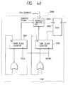
Figure 47 is a block diagram of this
embodiment, which has almost the same configuration
as Figure 46. Different components include an
input section 3100 and a display section 3101, which
are used to create graphic patterns, an input pattern
memory 3106 for storing created graphic patterns,
and a graphic pattern generation circuit 2088 for
generating created graphic patterns. The graphic
pattern generation circuit 2088 is shown in Figure
48. The operations will be described later.
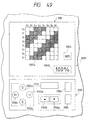
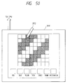
Figure 49 shows the configuration of an
operation unit for selecting and specifying graphic
patterns. 3099 denotes the operation unit,
comprising a graphic pattern input section 3100
and a graphic pattern display section 3101. The
graphic pattern input section 3100 consists of Up,
Down, Left, and Right position designation keys
3100a, 3100b, 3100c, and 3100d for designating the
positions of graphic patterns, a select key 3102
for specifying presence or absence of a graphic
pattern, reduction and enlargement variable power
keys 3103a and 3103b for freely changing the size
of an input graphic pattern by specifying an intended
magnifying power, a pattern registration key 3104
for registering graphic patterns, and a hue key
3105 for selecting a hue associated with a graphic
pattern.
The display section 3101 is a liquid crystal
display made up of multiple dots, including a first
display section 3101a for creating and displaying
graphic patterns using 64 blocks (8 x 8), a second
display section 3101b for indicating a magnifying
power specified with the variable power keys 3103a
and 3013b, and a third display section 3101c for
indicating a hue associated with an input graphic
pattern.
A graphic pattern is entered as follows;
a hue corresponding to an input graphic pattern
is selected using a Hue key 3105 and the third
display section 3101c, 64 blocks displayed in the
first display section 3101a are specified sequentially
from X0 to X7 laterally and Y0 to Y7 vertically
using the Up, Down, Left, and Right position
designation keys 3100a to 3100d, and presence or
absence of a graphic pattern is specified for each
of the blocks using the Select key 3102. For example,
in this embodiment, when a graphic pattern is
designated as shown in the first display section
3101a of Figure 47, the mesh graphic pattern in
which oblique lines are intercrossing is entered.
When specifying presence or absence of a
graphic pattern for all 64 blocks is completed,
a Pattern Registration key 3104 is pressed. Then,
the designated graphic pattern is placed in an
input pattern memory 3106 made up of a ROM and a
RAM shown in Figure 47. Moreover, a coefficient
corresponding to a magnifying power specified using
the variable power keys 3103a and 3103b is calculated
by a CPU 3107 shown in Figure 47 and written in
a graphic pattern RAM 3095 of a graphic pattern
generation circuit 2088 shown in Figure 48. At
this time, addresses of the RAM 3095 are switched
to CPU addresses with a control signal fed to an
address control 3109. Then, the input graphic pattern
signal is written in the graphic pattern RAM 3095.
When writing the graphic pattern signal in the RAM
3095 is completed, the addresses are returned to
an address control circuit 2089 shown in Figure
47 with a control signal.
As described previously, a graphic pattern
signal thus provided is displayed in an area
corresponding to a color signal in an image. Then,
a monochrome image on which any input graphic pattern
is added in a size of a specified magnifying power
is printed by a printer 2102. Thus, a monochrome
processed image on which the graphic patterns
corresponding to the colors of images in an original
are added is made available.
In this embodiment, graphic patterns are
entered by operating the display section 3101 and
input section 3100 of the operation unit 3099.
A graphic pattern setting means is not limited to
those equipment, but may be made up of an editor
3111 and an input pen 3112 shown in Figure 50.
Thus, graphic patterns may be entered. When the
editor 3111 is implemented, the input pen 3112 is
used to enter positions in X and Y direction. In
this case, as described in the previous embodiment,
a graphic pattern is designated for each of 64 blocks
using the input pen 3112, then a hue associated
with the designated graphic pattern is specified
in an area for indicating hues in a lower part of
the display section 3101. Thus, any graphic pattern
can be entered.
This embodiment employs a reader as an
information generation means. However, the embodiment
may apply to an image processing apparatus for printing
VTR outputs or computer outputs. The printer for
the embodiment is not limited to an electrophotographic
printer, but may be an ink-jet printer,
a thermal printer, or other various types of printers.
The embodiment is applicable to not only printers
but also other output units; such as, CRTs, liquid
crystal displays, or other monochrome monitors.
As described so far, color information an
information generation means has generated is
assessed to detect the colors of color images in
an original. The color detection signals are
checked to learn colors, then any graphic patterns
are specified for the colors using a pattern setting
means. Therefore, when even a low-priced monotone
printer is installed, it is possible to provide
monotone processed images which permits effortless
and accurate identification of the colors of pixels
in the color images in an original.