This invention relates to a method of modulating
and demodulating digital data and also to a digital
data modulator/demodulator.
Various methods have been developed for modulating
digital data to be recorded on a recording medium in an
attempt to make the modulating method adapted to the
characteristics of the recording medium. Specifically,
in the field of magnetic recording, each original data
is typically converted and modulated into a code
according to a rule for minimizing the DC components
and the number of consecutive hits with a same polarity
such as 8-10 modulation or 8-14 modulation before it is
recorded.
Jpn. Pat. Appln. KOKAI Publication No. 52-11916
proposes a modulation method of converting a data into
a code having no DC component by allowing the number of
bits thereof to have a certain degree of redundancy.
For example, it discloses a technique of selecting 16
codes out of 20 6-bit codes having no DC component in
order to establish a one-to-one correspondence between
them and 16 4-bit codes.
Jpn. Pat. Appln. KOKAI Publication No. 60-12840
proposes a method of converting a 4-bit data into a
6-bit data. With the proposed method, out of 64
different 6-bit data, 16 having no three or more than
three consecutive "1"s or "0"s will be selected.
For instance, a logic circuit may be used to convert a
4-bit data into a 6-bit data of the type as described
above. The proposed method uses a convert table for
obtaining 6-bit data where the number of "1"s is odd
and whose least significant bit is generated by means
of odd parity of the remaining 5 bits. Additionally,
if there appear 4 consecutive "1"s or "0"s as a result
of coupling modulation codes, using odd parity, the
number of consecutive "1"s or "0"s is reduced to 2 by
means of bit inversion.
On the other hand, the applicant of the present
patent application proposed in EP 0 670 555 Al
(corresponding to USSN 08/407,018) a set of dot codes
arranged in the form of an optically readable code
pattern and recorded on a recording medium such as a
sheet of paper and an apparatus for reproducing the
recorded dot codes by scanning the pattern. According
to this invention, dot codes are modulated before being
recorded in such a way that given data are transformed
into a pattern of dot codes different from any marker
(which consists of a predetermined number of
consecutive black dots on the sheet of paper operating
as recording medium). When a marker is recorded as a
number of consecutive black dots, the modulated data
(a dot image pattern) may contain any number of
consecutive white dots. Thus, the applicant of the
present patent application proposed a modulation method
for limiting the number of consecutive black dots in a
dot image pattern, disregarding the number of
consecutive white dots in EP 0 765 041 A2
(corresponding to USSN 08/696,003).
With any of the above described modulation methods,
modulation codes are arranged in the form of a table
adapted to correspond to all input data strings and
stored in a ROM (read only memory).
When reproduced, the modulation codes can
violate the modulation rule due to errors in the
magneto-electric transformation system when a magnetic
recording medium is used or in the image pick-up system
(including the use of a binarization process) if a
recording system of recording data on a sheet of paper
is used. USP 5,406,569 describes a method for reducing
such errors. The disclosed system will be summarily
discussed below.
A modulation code that violates the rule is
compared with each of the modulated reference codes
prepared on the basis of all the modulation codes in
the demodulation table for 1 to 1 correspondence to
determine the Hamming distance between itself and the
modulated reference code and the modulation code that
is violating the rule is transformed into the modulated
reference code showing the shortest Hamming distance to
it. If there are found two or more than two modulated
reference codes that show a same Hamming distance to
the violator, each of the bits of the modulation code
is weighted on the basis of the probability of
occurrence of an error of the bit and the competing
reference codes are examined in terms of the weighted
bits to determine the modulated reference code showing
the shortest Hamming distance to the violator in order
to improve the error correction capability.
However, with the method as disclosed in the above
cited USP 5,406,569, there can remain more than one
modulated reference codes that shows a same Hamming
distance to the violator after the weighting operation.
Then, the method is helpless for error correction and
can only detect errors. Additionally, the above
discussed method is rather cumbersome because it has to
determine the Hamming distance between a modulation
code detected as a rule violator and each of the
modulated reference does.
The above cited Jpn. Pat. Appln. KOKAI Publication
No. 52-11916 describes a method of detecting a
modulation code that violates the modulation rule
by means of the redundancy inherent to the modulation
code. Again, however, this method is helpless
for error correction and can only detect errors.
Jpn. Pat. Appln. KOKAI Publication No. 62-12840 also
discloses a method of detecting errors by means of odd
parity that cannot correct errors either. Particularly,
this method becomes helpless even for error detection
if the parity bit is inverted when two modulation codes
are coupled to produce four consecutive "1"s or "0"s.
In view of the above identified problems of the
prior art, it is therefore the object of the present
invention to provide a method of modulating and
demodulating digital data that can detect and correct
errors in a simple manner. Another object of the
invention is to provide a digital data
modulator/demodulator using such a method.
According to a first aspect of the present
invention, there is provided a method of modulating
digital data to be used for transmitting or recording
N-bit data, comprising steps of:
According to a second aspect of the present
invention, there is provided a method of modulating
digital data to be used for transmitting or recording
N-bit data, comprising steps of:
According to a third aspect of the present
invention, there is provided a method of modulating
digital data to be used for transmitting or recording
N-bit data, comprising steps of:
According to a fourth aspect of the present
invention, there is provided a method of demodulating
an M+K-bit digital data obtained by a digital data
modulating method of converting N-bit data into an
M+K-bit data selected out of a group of 2
M M+K-bit
data according to a predetermined rule, the group of 2
M
M+K-bit data being obtained by adding a K-bit error
correction checking symbol to M-bit data (N<M), back
into N-bit data, comprising steps of:
According to a fifth aspect of the present
invention, there is provided a method of demodulating
an M+K-bit digital data obtained by a digital data
modulating method of converting the input N-bit into an
M+K-bit data selected out of a group of L×2
M M+K-bit
data according to a predetermined rule, the group of
L×2
M M+K-bit data being obtained by adding K-bit error
correction checking symbols generated on the basis of L
error correcting generation polynomials to M-bit data
(N<M) on a one by one basis and in terms of Hamming
distance greater than a predetermined value, into an
N-bit data, comprising steps of:
According to a sixth aspect of the present
invention, there is provided a method of demodulating
an M
i+K
i-bit digital data obtained by a digital
data modulating method of converting by means of
a converting method selected out of R different
converting methods the input N-bit into an M
i+K
i-bit
data selected out of a group of 2
Mi M
i+K
i-bit data
according to a predetermined rule, the group of 2
Mi
M
i+K
i-bit data being obtained by adding K
i-bit error
correction checking symbols (K
i being 0 or a positive
integer) to M
i-bit data (N<M; i=0, 1, 2, 3, ..., R-1)
on a one by one basis, the digital data modulating
method including a step of outputting the obtained
M
i+K
i-bit digital data along with information data
showing the selected converting method, into an N-bit
data, comprising steps of:
According to a seventh aspect of the present
invention, there is provided a digital data modulator
to be used for transmitting or recording N-bit data,
comprising:
According to an eighth aspect of the present
invention, there is provided a digital data modulator
to be used for transmitting or recording N-bit data,
comprising:
According to a ninth aspect of the present
invention, there is provided a digital data modulator
to be used for transmitting or recording N-bit data,
comprising:
According to a tenth aspect of the present
invention, there is provided a digital data demodulator
for demodulating an M+K-bit digital data obtained by
a digital data modulating method of converting N-bit
data into an M+K-bit data selected out of a group of 2
M
M+K-bit data according to a predetermined rule,
the group of 2
M M+K-bit data being obtained by adding
a K-bit error correction checking symbol to M-bit data
(N<M), back into N-bit data, comprising:
According to a eleventh aspect of the present
invention, there is provided a digital data demodulator
for demodulating an M+K-bit digital data obtained by a
digital data modulating method of converting the input
N-bit into an M+K-bit data selected out of a group of
L×2
M M+K-bit data according to a predetermined rule,
the group of L×2
M M+K-bit data being obtained by adding
K-bit error correction checking symbols generated on
the basis of L error correcting generation polynomials
to M-bit data (N<M) on a one by one basis and in terms
of Hamming distance greater than a predetermined value,
into an N-bit data, comprising:
According to a twelfth aspect of the present
invention, there is provided a digital data demodulator
for demodulating an M
i+K
i-bit digital data obtained by
a digital data modulating method of converting by means
of a converting method selected out of R different
converting methods the input N-bit into an M
i+K
i-bit
data selected out of a group of 2
Mi M
i+K
i-bit data
according to a predetermined rule, the group of 2
Mi
M
i+K
i-bit data being obtained by adding K
i-bit error
correction checking symbols (K
i being 0 or a positive
integer) to M
i-bit data (N<M; i=0, 1, 2, 3, ..., R-1)
on a one by one basis, the digital data modulating
method including a step of outputting the obtained
M
i+K
i-bit digital data along with information data
showing the selected converting method, into an N-bit
data, comprising:
According to a thirteenth aspect of the present
invention, there is provided a method of modulating
digital data to be used for printing and recording an
N-bit data on a predetermined medium as optically
readable code pattern, wherein
This invention can be more fully understood from
the following detailed description when taken in
conjunction with the accompanying drawings, in which:
Embodiments of the present invention will be
described below.
[1st Embodiment]
Now, a modulation method and a modulator according
to the invention will be described by referring to the
first embodiment.
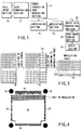
FIG. 1 is a schematic block diagram of a dot code
recording apparatus to which the first embodiment of
modulation method and modulator according to the
invention are applied. The dot code recording
apparatus comprises a data input section 10, a data
compressing section 12, an error correction code
generating section 14, an interleaving section 16, a
modulating section 18, a block data generating section
20, a code image forming section 22 and an output
section 24.
The data input section 10 is used to input
multimedia information including voice, image and text
and transform them into digital data. The data
compressing section 12 operates to compress the digital
data produced from the data input section 10 by
transforming the input data in a predetermined manner.
The error correction code generating section 14 adds an
error correction checking symbol to the data compressed
by the data compressing section 12 and generates error
correction codes. The interleaving section 16 performs
an interleaving operation to the error correction codes
generated by the error correction code generating
section 14. The modulating section 18 converts the
data interleaved by the interleaving section 16 into
modulation codes (as will be described in greater
detail hereinafter). The block data generating section
20 collects a predetermined number of modulation codes
converted by the modulating section 18 to form a block
and generates and adds a header to the block. The code
image forming section 22 generates image data in the
form of a code pattern 26 of dot codes as shown in
FIG. 2 from the data of the block generated by the
block data generating section 20. In other words, it
transforms the block data into black and white dots in
block header 28 and block user data 30 regions for the
code pattern 26 of dot codes and generates image data
out of them that are accompanied by markers 32 and
pattern codes 34. Finally, the output section 24
outputs the image data of the code pattern 26 generated
by the code image forming section 22 to a printer or
some other recording device.
In the following description, voice is used
for input data and any error correction code is a
Reed-Solomon code. Additionally, the output code image
will be a bit map image of an optically readable code
pattern 26 as shown in FIG. 2 that comprises one or
more than one blocks 36, each of which constituted by
a block header 28, block user data 30 including a
plurality of dot images, a marker 32 and a pattern
code 34, although the present invention is not limited
thereto in any means.
Now, the operation of the first embodiment will be
described in detail.
Firstly, voice information entered by way of a
microphone (not shown) is subjected to A/D conversion
and transformed into digital voice in the data input
section 10.
The digital voice obtained by the transformation
is then subjected to a data compressing operation of
waveform coding such as ADPCM (adaptive differential
pulse code modulation) or of analytic/synthetic coding
such as CELP (code excited linear prediction).
Additionally, identification data for identifying
(the data type, the compression ratio and mode, the
data volume, etc. of) the input data and the data
compressing operation are added as header to the
compressed voice data, which are then sent into the
error correction code generating section 14.
Then, an error correction code checking symbol is
added to every predetermined number of bytes of the
compressed voice data entered to the error correction
code generating section 14. Any error correction code
checking symbol as used herein is a Reed-Solomon code
checking symbol. For example, an error correction code
checking symbol of 16 bytes may be added to every 72
bytes of data. The Reed-Solomon code generating
polynomial as used in this embodiment has roots of αℓ,
aℓ+1, ..., αℓ+d-2 for primitive element α on Galois
field GF(28), where d represents the smallest Hamming
distance and ℓ represents a positive integer equal to or
smaller than 254-(d-2), which may be equal to zero.
Then, a plurality of 88 bytes Reed-Solomon codes, each
having a checking symbol, are entered to the
interleaving section 16.
The plurality of Reed-Solomon codes entered to the
interleaving section 16 are temporarily stored in an
internal memory (not shown). Then, the stored data are
interleaved when a predetermined number of Reed-Solomon
codes are accumulated there or according to the
accumulated number of codes so that they can readily be
used to cope with burst errors. The interleaving
method and the format of correction code are described
the header (which is a macro block header as described
in EP 0 713 194 A1 (corresponding to USSN 08/586,792)
proposed by the applicant of the present patent
application). The header is then inserted into and
added to the interleaved data in a distributed manner
according to the volume of the data stored in the
memory. A description of the rule for the distribution
and the insertion (macro block header distribution
information) is then entered to the block data
generating section 20 and recorded in the block
header 28 as will be described hereinafter. The
interleaved data and header are modulated by every
unit of bytes for the above error correction and then
input to the modulating section 18 (although a byte
unit of a Reed-Solomon code corresponds to 8 bits in
this embodiment, it does not necessarily have to do so
long as it is equal to a data unit to be modulated
(as will be described hereinafter)).
Each byte data entered to the modulating section
18 corresponds to an address of the built-in modulation
table ROM (not shown) and the contents of the address
are output to the block data generating section 20 as a
modulation code.
Now, the contents of the modulation table will
be described below in detail. Note that the modulation
rule of an optically readable code pattern printed
on a sheet of paper as shown in FIG. 2 will be
described, although the modulation rule depends on the
transmission mode, the characteristics of the recording
medium and the contents of the physical data format.
A code pattern 26 comprises blocks 36, each of
which by turn comprises a marker 32 to be used as
reference, a pattern code 34, a block header 28 and
block user data 30. Since the method for optically
reading a code pattern 26 as used herein is described
in detail in EP 0 717 398 A2 (corresponding to
USSN 08/571,776) filed by the applicant of the present
patent application, it will be described only briefly
below.
It is a method with which an image of the code
pattern 26 is picked up by means of an image pick-up
system and markers 32 are detected from the binarized
image that is obtained from the picked-up image to
precisely determine the location where the operation of
reading the block header 28 and the block user data 30
is conducted so that each 1-bit data can be retrieved
as a white or black dot at the determined location.
With this technique, the markers 32 have to be
detected firstly from the picked-up binary image.
Particularly care should be taken when a marker is
detected as a region of consecutive black dots and a
same pattern of consecutive black dots is be detected
also in the remaining regions, particularly in the
block user data 30, because the latter is erroneously
recognized as a marker so that consequently the
subsequent operation of detecting the pattern code 34
and reading the block header 28 and the block user
data 30 will be baffled.
In order to avoid detection of wrong markers, the
block user data 30 are modulated so that a pattern same
as that of any of the markers 32 operating as reference
may not appear. The rule used for the modulation in
this embodiment is described in EP 0 765 041 A2
(corresponding to USSN 08/696,003) filed by the
applicant of the present patent application, according
to which no three or more than three consecutive dots
will be arranged in the direction parallel with the
pattern code 34, although the number may vary depending
on the size of the markers 32 and hence is not fixed in
any means.
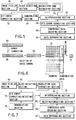
FIG. 3 is a schematic illustration showing how a
modulation table is prepared in this embodiment.
Referring to FIG. 3, firstly a 13-bit data 42 will be
formed from each of a total of 512 9-bit (=M) data 38
by adding a 4-bit (=K) error correction code checking
symbol 40 thereto as error correction code. Note that
"9" is selected as a number greater than the number of
bits of a byte (which is equal to "8" (=N) in this
embodiment). The error correction code is a BCH
(Bose-Chaudhuri-Hocquenghem) code formed by means of
generation polynomial G(x)=x4+x3+1 having original
element α of Galois field GF (24) as root. The
checking symbol (4-bit) may be subjected to a bit
inversion or alternatively generation polynomial
G(x)=x4+x+1 may be used. Bit inversion provides an
effect of detecting, as an error, a code whose bits are
all "0"s that can be generated for some reason or
another.
Then, 256 13-bit data will be selected as
modulation codes 44 out of the generated 512 13-bit
data according to the modulation rule. The modulation
rule provides that there shall be 3 or less consecutive
"1"s in each 13-bit data and neither the most nor the
least significant bit shall be related to more than 2
consecutive "1"s. With this arrangement, the number of
consecutive "1"s in a data string obtained by coupling
a plurality of 13-bit modulation codes will not exceed
four.
Then, the selected 256 modulation codes 44 are
made to show one-to-one correspondence with the byte
data before the modulation. This procedure is
reflected by the cost particularly when a logic circuit
is used for demodulation. The above procedure will not
be described here any further because the demodulation
process is based on a ROM table in this embodiment.
The 13-bit modulation codes are then entered to
the block data generating section 20 and collected for
the number equal to the number of recordable modulation
codes of the block user data 30 in the code pattern 26
shown in FIG. 2 to produce block user data information.
Additionally, a block address and the above described
macro bock header distributing information sent from
the interleaving section 16 are arranged at respective
predetermined bit positions of each piece of the block
user data information and an error correction code
checking symbol (a BCH code checking symbol) is added
thereto to generate block header information. Then,
block data containing block header information and user
data information as a unit will be generated.
The above block data are then entered to the code
image forming section 22 to produce a bit map image of
the code pattern 26. More specifically, each of the
bits used for the block header information is
transformed for the corresponding black or white dot of
the block header 28, while each of the above 13 bits is
transformed for the corresponding black or white dot
image in the block user data 30. Note that a bit is
transformed into a black dot if it is equal to "1",
whereas it is transformed into a white dot if it is
equal to "0". Also note that white dots will not have
to be printed at all.
The block user data are arranged from the block 36
at the upper left corner and in parallel with the
pattern code 34. Then, marker 32 and pattern code 34
are added to the predetermined respective positions of
the block by the code image forming section 22 to
produce a complete block. In the code pattern 26, each
block shares regions for marker 32, pattern code 34 and
block header 28 with adjacently located blocks.
Then, the number of consecutive black dots of any
two blocks that are located adjacently in the direction
parallel to the pattern codes 34 can be held equal to
or less than a predetermined number (5 in this
embodiment) by defining the modulation rule to arrange
the physical format of the code pattern 26 in order to
agree a partition for the modulation codes with the
boundary of the unmodulated block header 28 and the
modulated block user data 30.
While the logical structure of the block header 28
and the block user data 30 is not described in detail
above, it may preferably be identical with the one
described in EP 0 713 194 A1 (corresponding to
USSN 08/586,792).
While block data are prepared by the block data
generating section 20 after producing modulation
codes 44 in the above embodiment, alternatively, block
data may be prepared prior to modulation codes and
recorded as part of block user data 30 while the latter
are modulated in the code image forming section 22.
The bit map image of the generated code pattern 26
is then transmitted from the code image forming section
22 to the output section 24, which transforms it into
data that can be recognized by a printing press or a
printer and outputs them to the latter.
Thus, the modulation codes modulated by the above
described modulating method are recorded as an
optically readable dot image that is free from the
detection of wrong markers so that errors that can
occur at the time of demodulation due to blurred and/or
expanded dots and stains adhering to the sheet of paper
after the printing can be eliminated effectively and
efficiently to minimize the error rate after the
demodulation.
[2nd Embodiment]
Now, a demodulation method and a demodulator
according to the invention will be described by
referring to the second embodiment.
FIG. 5 is a schematic block diagram of a dot
code reproducing apparatus to which the second
embodiment of demodulation method and demodulator
according to the invention are applied. The dot code
reproducing apparatus comprises an image pick-up
section 46, a block detecting section 48, a modulation
code extracting section 50, a bit error correcting
section 52, a demodulating section 54, a deinterleaving
section 56, a byte error correcting section 58, a
compressed data decoding section 60 and a data
reproducing section 62.
The image pick-up section 46 picks up an optically
readable code pattern and generates a digital image.
The block detecting section 48 detects blocks of dot
codes from the generated digital image and extracts
the black header of each of the detected blocks.
The modulation code extracting section 50 extracts
modulation codes from the block user data and the bit
error correcting section 52 operates to correct errors
that can be found in the extracted modulation codes.
The demodulating section 54 generates demodulation data
for the modulation codes that have been subjected to a
bit error correcting operation of the bit error
correcting section 52. The deinterleaving section 56
temporarily stores the demodulation data generated by
the demodulating section 54 in an internal memory
(not shown) and rearranges the plurality of pieces of
demodulation data stored in the memory. The byte error
correcting section 58 performs a byte error correcting
operation on the rearranged pieces of demodulation data
and the compressed data decoding section 60 decodes the
compressed data that have been corrected for byte
errors by decompressing them to restore the original
multimedia data in the form of a combination of voice,
image and text. The data reproducing section 62
transforms the restored multimedia data into data that
can be recognized by an output unit (not shown) and
sends them to the output unit.
While it is assumed here that the code pattern has
a configuration as shown in FIG. 2 and modulation codes
are 13-bit modulation codes as described by referring
to the first embodiment, whereas the operation of bit
error correction and that of byte error correction are
respectively an operation of correcting BCH codes and
that of correcting Reed-Solomon codes and data are
output as voice data, it should be noted that the
present invention is not limited thereto in any means.
Now, the operation of the second embodiment will
be described in detail.
The image pick-up section 46 picks up an image of
the code pattern 26 typically by means of a CCD camera
and binarizes it to produce a binarized image.
The produced binarized image is then entered to
the block detecting section 48, which detects blocks 36
from the entered binarized image and determines the
positions for reading the block header 28 and the block
user data 30. Then, the block address and the macro
block header distribution information contained in
the block header 28 read out at the determined reading
position are transmitted to the deinterleaving
section 56. The logical structure of the block address
and that of the macro block header distribution
information are described in detail in EP 0 713 194 A1
(corresponding to USSN 08/586,792) filed by the
applicant of the present patent application and hence
will not be described here.
The modulation code extracting section 50
determines each of the bits read out at the position
for reading the block user data for black or white
and transforms them into bit data in order to extract
13-bit modulation codes.
Then, the extracted modulation codes are
demodulated in a manner as described below by also
referring to FIG. 6.
The 13-bit modulation codes 64 extracted by the
modulation code extracting section 50 are then entered
to the bit error correcting section 52 for error
correction. The error correcting operation of the bit
error correcting section 52 is an operation of decoding
BCH codes as will be briefly described below.
Firstly, syndrome s is determined from
multiplication of 13-bit modulation code 64 which is
expressed by V and check matrix H;
s = H·V
where H is expressed by equation below;
H = (α12, α11, α10, α9, α8, α7, α6, α5, α4,
α3, α2, α, 1), α being the primitive element of
GF(24).
The above modulation code V is expressed by
addition of error-free modulation code V0 and error
vector ε (=exclusive logical OR) and therefore syndrome
s is also expressed by equation below;
s = H·V = H·(V0+ε) = H·V0 + H·ε = H·ε,
where H·V0 = 0.
For example, if the least significant bit of
modulation code V is the 0-th bit and the seventh bit
has an error, then error vector ε will be expressed as
follows.
ε = (0, 0, 0, 0, 0, 1, 0, 0, 0, 0, 0, 0, 0)
Then, syndrome s will be expressed as follows.
s = α7
Thus, the bit position where syndrome s shows the
7-th power contains an error so that the operation of
correcting a 1-bit error is reliably performed by
inverting the bit position.
The smallest Hamming distance of a 13-bit
modulation code that can be used for this embodiment is
equal to 3 and, therefore this embodiment is so adapted
that it can correct only a single 1-bit error. In
other words, if there occurs an error for two or more
than two bits in a modulation code with this embodiment,
multiple error correcting operations can take place to
consequently increase the number of bit errors. On the
other hand, the operation of correcting byte errors of
the byte error correcting section 58 is conducted on
the basis of an error unit of a byte as will be
described hereinafter and, therefore, a byte error can
contain a plurality of bit errors in a byte. Thus,
the number of bit errors given rise to by multiple
error correcting operations can be limited to the
number of bits in a byte by making a modulation code
(a demodulation data) correspond to a byte.
Therefore, if the number of bit errors is raised
by multiple error correcting operations in each
demodulation data, the number of byte errors and hence
the outcome of byte error correcting operations of the
embodiment will not be affected at all as a result.
Conversely, since a modulation code containing a bit
error can be corrected perfectly, the number of bit
errors immediately prior to a byte error correcting
operation will be reduced without fail to dramatically
improve the final error rate that can be obtained when
the byte error correcting process is completed.
The modulation codes 66 that have been subjected
to an error correcting process are then entered to the
demodulating section 54, where the error correction
checking symbol (4 bits) is removed from each
modulation code to produce a 9-bit data, which is then
used as an address 68 of the 9-bit demodulation
table 70. Then, the 8-bit data of the demodulation
table 70 that corresponds to the produced address 68
is entered to the deinterleaving section 56 as
demodulation data.
The above described processing operation of the
demodulating section 54 utilizes a demodulation
table 70 to demodulate modulation codes. It will be
appreciated that the error correction checking symbol
is removed from each 13-bit data to reduce the number
of bits of each reference address from thirteen to nine
in order to minimize the size of the demodulation table.
However, it will be appreciated that the demodulating
operation can be conducted by means of a logic circuit
(which may include logical AND, OR and/or NOT circuits)
without using a demodulation table. If such is the
case, a data from which the error correction checking
symbols is removed may devoid of information effective
for logical operations and consequently a large circuit
may be required to handle such data. Therefore, in
this case, a 13-bit data is preferably sent directly to
the logic circuit without removing the error correction
checking symbols therefrom to output a 8-bit data.
The demodulation data 72 sent to the
deinterleaving section 56 is then temporarily stored
in an internal memory (not shown) and, when the
demodulation data stored in the memory get to a
predetermined volume that is based on the interleave-related
information contained in the headers located in
the respective positions determined by means of the
macro block header distribution information, the stored
pieces of demodulation data are rearranged on the
basis of unit to generate an error correction code
(Reed-Solomon code) to be used for the error correcting
operation of the byte error correcting section 58.
The rearranging operation is exactly the reverse of the
interleaving operation conducted at the time of
generating codes.
The correction code to be used by the byte error
correcting section 58 is a Reed-Solomon code that
handles a demodulation data 72 as a byte as described
above and, therefore, the generating polynomial has
roots of αℓ, αℓ+1, ..., αℓ+d-2 for primitive element α
of GF(28), where d represents the smallest Hamming
distance and ℓ represents a positive integer equal to or
smaller than 254-(d-2), which may be equal to zero.
Since the procedure of decoding a Reed-Solomon
code is not essential to the present invention, it will
be described only briefly below.
Firstly, syndrome SRS is determined from
multiplication of check matrix HRS and Reed-Solomon
code VRS.
Then, error position polynomial σ(x) and error
pattern polynomial ω(x) are determined from the
obtained syndrome SRS by means of the Euclidean
algorithm. The roots of the determined error position
polynomial σ(x) are then determined by the chain search
technique to determine the error positions. Finally,
an error pattern is produced from the roots of the
error position polynomial σ(x) and the error pattern
polynomial ω(x). The relationship between the number
of errors L of a Reed-Solomon code that can be
corrected and the smallest Hamming distance d is
expressed by the formula below.
2L ≦ d - 1
A Reed-Solomon code is uncorrectable (including
error correction) unless the number of byte errors in
the code satisfies the above formula. Thus, the number
of byte errors is reduced by bit error correction at
the time of demodulating the modulation code before the
Reed-Solomon code correcting operation to significantly
reduced the probability of unable correction for the
Reed-Solomon code.
The compressed voice data obtained after the above
described operation of correcting the Reed-Solomon code
are then entered to the compressed data decoding
section 60, which decodes the compressed data by
following a predetermined procedure to restore the
original voice data. The restored voice data are
then entered to the data reproducing section 62,
which carries out an N-times over-sampling operation,
a low-pass filtering operation and an operation of D/A
conversion on the entered voice data before they are
sent to an amplifier.
With the operation of reading an optically
readable code pattern of modulation codes produced by
means of the above described modulating method, the
modulation codes in each block can be extracted without
detecting wrong markers and a predetermined number of
errors that can occur in any of the modulation codes in
the demodulating step can be reliably corrected so that
the error correction capability of the subsequent steps
does not have to be enhanced disproportionally and the
data error rate of the output voice data can be
minimized. Additionally, the use of a recording medium
that inherently shows a high error rate can be made
feasible. (Note that, in the case of high quality or
medium quality paper, ink or toner may not wet the
paper evenly and blurred and/or expanded dots can
appear frequently to give rise to a high error rate on
a dot basis).
While errors are not detected during the error
correcting operation at the time of demodulating
modulation codes in the above description, it will be
appreciated that errors can be detected without problem
at the time of demodulating modulation codes and the
information obtained through the error detecting
operation can be used by the byte error correcting
section 58 as deletion-related information (information
for identifying demodulation errors). If only an error
detecting operation is conducted at the time of
demodulating modulation codes, up to two bit errors can
be reliable detected in each 13-bit modulation code so
that the deletion-related information (information for
identifying demodulation errors) can also reliably be
detected to effectively exploit the potential of
correcting and/or deleting data.
[3rd Embodiment]
Now, a demodulation method and a demodulator
according to the invention will be described by
referring to the third embodiment.
FIG. 7 is a schematic block diagram of a dot code
reproducing apparatus to which the third embodiment of
demodulation method and demodulator according to the
invention are applied. The dot code reproducing
apparatus comprises an image pick-up section 46, a
block detecting section 48, a modulation code
extracting section 50, a bit error correction detecting
section 74, a demodulating section 76, a deinterleaving
section 78, a deleting/correcting section 80, a
compressed data decoding section 82 and a data
reproducing section 62.
The image pick-up section 46 picks up an optically
readable code pattern and generates a digital image.
The block detecting section 48 detects blocks of dot
codes from the generated digital image and extracts the
black header of each of the detected blocks. The
modulation code extracting section 50 extracts
modulation codes from the block user data.
The bit error correction detecting section 74
operates to correct errors of a plurality of different
types that can exist in the modulation codes extracted
by the modulation code extracting section 50. The
demodulating section 76 generates demodulation data for
each of the modulation codes that have been subjected
to a bit error correcting operation of the bit error
correction detecting section 74 and selects one of them.
It also outputs information for identifying
demodulation errors. The deinterleaving section 78
temporarily stores the demodulation data and the
information for identifying demodulation errors
generated by the demodulating section 76 in an internal
memory (not shown) and rearranges the plurality of
pieces of demodulation data and those of information
for identifying demodulation errors stored in the
memory. The deleting/correcting section 80 operates
for deleting/correcting data on the rearranged pieces
of demodulation data on the basis of the rearranged
pieces of information for identifying demodulation
errors and the compressed data decoding section 82
decompress and decodes the compressed data that have
been subjected to a byte error correcting operation to
restore the original multimedia data in the form of a
combination of voice, image and text.
The data reproducing section 62 transforms the
restored multimedia data into data that can be
recognized by an output unit and sends them to the
output unit.
While it is assumed here that the code pattern has
a configuration as shown in FIG. 2 and the
deleting/correcting operation is that of correcting
Reed-Solomon codes, whereas data are output as voice
data, it should be noted that the present invention is
not limited thereto in any means.
Now, the operation of the third embodiment will be
described in detail. The steps from that of picking a
code pattern 26 to that of extracting modulation codes
are identical with those of the second embodiment and
hence will not be described here.
FIG. 8 shows the modulation rule to be applied to
the modulation codes that have been extracted in a
manner as described above.
While the modulation rule of this embodiment is
same as that of the first embodiment to the extent that
8-bit data are converted into 13-bit data, they differ
from each other as described below.
Referring to FIG. 8, firstly, a 4-bit error
correction checking signal is added to each of a total
of 512 9-bit data 84 to generate two different sets of
13-bit BCH codes 86, 88. The first set of BCH codes 86
is formed from generation polynomial G1(x)=x4+x3+1
having original element α of Galois field GF (24).
The second set of BCH codes 88 is formed from
generation polynomial G2(x)=x4+x+1 having original
element β of Galois field GF (24).
Then, codes conforming to the modulation rule that
there shall be 3 or less consecutive "1"s in each bit
data and the most significant bit shall not be related
to more than 2 consecutive "1"s, while the least
significant bit shall not be related to any consecutive
"1"s if it is "1" (or vice versa) will be selected
from each of the two sets of BCH codes 86, 88 to
generate a first modulation table 90 and a second
modulation table 92 respectively. The modulation
tables 90, 92 contains 253 modulation codes and 252
modulation codes respectively. The third modulation
table 94 shown is formed by selecting 256 modulation
codes from the modulation codes of the first and second
modulation tables 90, 92. With the third modulation
table 94, no consecutive four "1"s will be generated.
While each of the first and second modulation
tables 90, 92 is constituted of a group of modulation
codes having the shortest Hamming distance 3,
modulation codes showing a large Hamming distance
should be selected because the shortest Hamming
distance can become too short when the modulation codes
of the groups are mixed with each other. For example,
all the 253 modulation codes of the first modulation
table 90 may be selected and the remaining three may be
selected from the second modulation table 92 in such a
way that the three show the shortest Hamming distance
of 2 with the 253 modulation codes of the first
modulation table 90.
With this arrangement, the third modulation
table 94 will be an unusual table where codes with the
shortest Hamming distance of 2 are mixed with the
remaining codes with the shortest Hamming distance of 3
(which are the 253 modulation codes of the first
modulation table 90).
With this unusual modulation table, 1-bit errors
that can be produced on a modulation code basis cannot
be reliably corrected. Particularly, when an
erroneously modulation code is located between a pair
of codes with the shortest Hamming distance of 2, it
will not be able to decide which one of the codes
should be used to correct the error.
FIG. 9 schematically shows the configuration of
the bit error correction detecting section 74 and the
demodulating section 76 adapted to the use of such an
unusual modulation table.
Firstly, modulation code V is input to the first
error correction detecting section 741 and the second
error correction detecting section 742 and then
syndrome s1 and s2 are determined respectively on the
basis of the check matrix H1 and the check matrix H2;
H1 = ( α12, α11, α10, α9, α8, α7, α6, α5, α4,
α3, α2, α,1), α being the primitive element of
GF(24),
H2 = (β12, β11, β10, β9, β8, β7, β6, β5, β4,
β3, β2, β, 1), β being the primitive element of
GF(24),
s1 = H1·V and s2 = H2·V.
Since syndromes s1 and s2 show error positions,
modulation code V is corrected to remove the 4-bit
error correction detecting symbol to produce 9-bit data
W1 and W2, which are then entered to the demodulating
section 76.
The demodulating section 76 is provided with a
first ROM table 761 having an address of 9-bit data W1
and adapted to output 8-bit demodulation data and a
second ROM table 762 having an address of W2 and
adapted to output 8-bit demodulation data. Each of the
ROM tables 761 and 762 contains a total of 512 8-bit
demodulation data.
The first ROM table 761 stores demodulation data
values that correspond to the 253 modulation codes of
the first modulation table 90 respectively at the
corresponding addresses. Then, one of the 3
demodulation data values (which represents dummy
demodulation data to be used for detecting demodulation
errors) that are not allocated to the first modulation
table 90 is stored at the remaining 259 addresses.
On the other hand, the second ROM table 762 stores
demodulation data values that correspond to the 3
modulation codes of the second modulation table 92
respectively at the corresponding addresses. Then, one
of the 253 demodulated values obtained by putting aside
the demodulation data corresponding to the 3 modulation
codes selected from the second modulation table 92
(which represents dummy demodulation data to be used
for detecting demodulation errors) is stored at the
remaining 509 addresses.
The 9-bit data W
1, W
2 output respectively from the
first error correction detecting section 74
1 and the
second error correction detecting section 74
2 are then
subjected to a demodulating operation conducted by
referring to the above two demodulation tables
(ROM tables 76
1 and 76
2) to generate demodulation data
F
1 and F
2. Error detection flag C
1 from the first
error correction detecting section 74
1 and error
detection flag C
2 from the second error correction
detecting section 74
2 are entered to the determining
section 76
3 along with the two demodulation data F
1, F
2,
which determining section 76
3 outputs a single
demodulation data F and demodulation error identifying
information C that corresponds to the demodulation data
under the following conditions.
where U
1 denotes a set of demodulation data
corresponding to the 253 modulation codes selected from
the first modulatlon table 90 and U
2 denotes a set of
demodulation data corresponding to the 3 modulation
codes selected from the second modulation table 92,
whereas
U 1 denotes a complementary set of U
1 and
U 2
denotes a complementary set of U
2. When both C
1 and C
2
are equal to "1", then it indicates detection of an
error. When both C
1 and C
2 are equal to "0" to the
contrary, then it indicates that no detection of error.
C denotes a demodulation error when it is equal to "1"
and no modulation error when it is equal to "0".
The method for determining demodulation data F and
demodulation error identifying information C that can
be used for the purpose of the invention is not limited
to the one as described above and, if there are two
candidates for demodulation data F, the right one may
be determined by weighting them with their respective
error appearing probabilities that have been computed
in advance for the given recording medium.
The demodulating section 76 operates to demodulate
modulation codes by referring to demodulation tables
and the number of reference addresses of the
demodulation tables is reduced from 13 bits to 9 bits
by removing the error correction checking symbol from
each demodulation data in order to minimize the size of
the demodulation tables in the above embodiment.
However, it will be appreciated that the demodulating
operation can be conducted by means of a logic circuit
(which may include logical AND, OR and/or NOT circuits)
without using a demodulation table. If such is the
case, a data from which the error correction checking
symbols is removed may devoid of information effective
for logical operations and consequently a large circuit
may be required to handle such data. Therefore, in
this case, a 13-bit data is preferably sent directly to
the logic circuit without removing the error correction
checking symbols therefrom to output a 8-bit data.
Demodulation data F and demodulation error
identifying information C are then entered to the
deinterleaving section 78 and temporarily stored in an
internal memory (not shown). When the demodulation
data stored in the memory get to a predetermined volume
that is based on the interleave-related information
contained in the headers located in the respective
positions determined by means of the macro block header
distribution information, the stored pieces of
demodulation data F and the corresponding pieces of
demodulation error identifying information C are
rearranged to generate an error correction code and a
flag string indicating the positions for deletion.
The error correction code and the deleting
position indicating flag string are then entered to the
deleting/correcting section 80. The correction code is
a Reed-Solomon code and the generating polynomial has
roots of aℓ, aℓ+1, ..., aℓ+d-2 for primitive element α
of GF(28).
Since the procedure of deleting/correcting
operation is not essential to the present invention, it
will be described only briefly below.
Firstly, syndrome SRS is determined from
multiplication of check matrix HRS and error correction
code VRS and then expressed in the form of syndrome
polynomial SRS(x).
Then, deleting position polynomial λ(x) is
determined from the deleting position indicating flag
string to generate TRS(x)=SRS(x)λ(x).
Then, error position polynomial σ(x) and error
pattern polynomial ω(x) are determined from TRS(x) by
means of the Euclidean algorithm. The roots of the
determined error position polynomial σ(x) are then
determined by the chain search technique to determine
the error positions. Finally, an error position, an
error pattern for the error position and a deletion
pattern are produced from the roots of the error
position polynomial σ(x), deleting position polynomial
λ(x) and the error pattern polynomial ω(x).
The relationship among the smallest distance d of
a error correction code, the number of errors L that
can be corrected and the number of deletions P is
expressed by the formula below.
2L + P ≦ d - 1
The use of deleting/correcting operation can
improve the error correcting capability if compared
with a case where no deletion is used. Particularly,
if all the error in a correction code are attributable
to deletion, the correcting capability is doubled from
the case where all error positions are indefinite.
The compressed data obtained after the above
described deleting/correcting operation are then
entered to the compressed data decoding section 82,
which decodes the compressed data by following a
predetermined procedure to restore the original voice
data. The restored voice data are then entered to
the data reproducing section 62, which carries out an
N-times over-sampling operation, a low-pass filtering
operation and an operation of D/A conversion on the
entered voice data before they are sent to an amplifier.
For the above described operation of reading
an optically readable code pattern of modulation
codes produced by means of the above described
modulating method, a relatively rigorous modulation
rule (for minimizing the number of consecutive
black dots) can be used to extract modulation codes
within a block without detecting wrong markers and a
predetermined number of errors that can occur in any
of the modulation codes can be reliably corrected
or detected in the demodulating step so that any
demodulation data having a detected demodulation error
can be deleted or corrected in a subsequent step to
minimize the overall data error rate and make it
possible to use a recording medium that inherently has
a high error rate.
[4th Embodiment]
Now, a modulation method and a modulator according
to the invention will be described by referring to the
fourth embodiment.
FIG. 10 is a schematic block diagram of a dot code
recording apparatus to which the fourth embodiment of
modulation method and modulator according to the
invention are applied. The dot code recording
apparatus comprises a data input section 10, a data
compressing section 12, an error correction code
generating section 14, an interleaving section 16, a
selecting section 96, a first modulating section 100, a
second modulating section 102, a block data generating
section 104, a code image forming section 22 and an
output section 24.
The data input section 10 is used to input
multimedia information in the form of a combination of
voice, image and text and transform them into digital
data. The data compressing section 12 operates to
compress the digital data produced from the data input
section 10 by transforming the input data in a
predetermined manner. The error correction code
generating section 14 adds an error correction checking
symbol to the data compressed by the data compressing
section 12 and generates error correction codes for the
data. The interleaving section 16 performs an
interleaving operation for the error correction code
generated by the error correction code generating
section 14.
The selecting section 96 selects either the first
modulating section 100 or the second modulating
section 102 according to modulation switching
information 106 and feeds it with the data interleaved
by the interleaving section 16. The first modulating
section 100 and the second modulating section 102,
whichever appropriate, converts the data fed to it into
modulation codes (as will be described in greater
detail hereinafter). The block data generating section
104 collects the modulation switching information 106
and a predetermined number of modulation codes to form
a block and generates and adds a header to the block to
produce block data.
The code image forming section 22 generates image
data in the form of a code pattern 26 of dot codes as
shown in FIG. 2 from the data of the block generated by
the block data generating section 104. In other words,
it transforms the block data into black and white dots
in block header 28 and block user data 30 regions for
the code pattern 26 of dot codes and generates image
data out of them that are accompanied by markers 32 and
pattern codes 34. Finally, the output section 24
outputs the image data of the code pattern 26 generated
by the code image forming section 22 to
a printer or some other recording device.
In the following description, voice is used for
input data and any error correction code is a Reed-Solomon
code. Additionally, the output code image will
be a bit map image of an optically readable code
pattern 26 as shown in FIG. 2 that comprises markers,
a pattern code and markers, although the present
invention is not limited thereto in any means.
Now, the operation of the first embodiment will be
described also by referring to FIG. 11.
Firstly, voice information entered by way of a
microphone (not shown) is subjected to A/D conversion
and transformed into digital voice in the data input
section 10.
The digital voice obtained by the transformation
is then subjected to a data compressing operation of
waveform coding such as ADPCM or of analytic/synthetic
coding such as CELP. Additionally, identification data
for identifying (the data type, the compression ratio
and mode, the data volume, etc. of) the input data and
the data compressing operation are added as header to
the compressed voice data, which are then sent into the
error correction code generating section 14.
Then, an error correction code checking symbol is
added to every predetermined number of bytes of the
compressed voice data entered to the error correction
code generating section 14. Any error correction code
checking symbol as used herein is a Reed-Solomon code
checking symbol. For example, an error correction code
checking symbol of 16 bytes may be added to every 72
bytes of data. The Reed-Solomon code generating
polynomial as used in this embodiment has roots of αℓ,
αℓ+1, ..., αℓ+d-2 for primitive element α on Galois
field GF(28), where d represents the smallest Hamming
distance and ℓ represents a positive integer equal to or
smaller than 254-(d-2), which may be equal to zero.
Then, a plurality of 88 bytes Reed-Solomon codes,
each having a checking symbol, are entered to the
interleaving section 16.
The plurality of Reed-Solomon codes entered to the
interleaving section 16 are temporarily stored in an
internal memory (not shown). Then, the stored data are
interleaved when a predetermined number of Reed-Solomon
codes are accumulated there or according to the
accumulated number of codes so that they can readily be
used to cope with burst errors. The interleaving
method and the format of correction code are described
the header (which is a macro block header as described
in EP 0 713 194 A1 (corresponding to USSN 08/586,792)
proposed by the applicant of the present patent
application). The header is then inserted into and
added to the interleaved data in a distributed manner
according to the volume of the data stored in the
memory. A description of the rule for the distribution
and the insertion (macro block header distribution
information) is then entered to the block data
generating section 104 and recorded in the block header
28 as will be described hereinafter. The interleaved
data and header are modulated by every unit of bytes
for the above error correction and then input to the
selecting section 96 (although a byte unit of a Reed-Solomon
code corresponds to 8 bits in this embodiment,
it does not necessarily have to do so long as it is
equal to a data unit to be modulated (as will be
described hereinafter)).
Each byte data entered to the selecting section 96
is the sent either the first modulating section 100 or
the second modulating section 102 according to the
modulation switching information 106. The modulation
switching information 106 will be selected according
to the recording medium selected by the code pattern
producer or determined automatically or manually
(by means of a table providing correspondence between
recording media and the types of modulation) at the
time of selecting the recording medium.
The reason for selecting the type of modulation
lies in the difference of error rate among various
recording media. Priority will be given to the error
correcting capability by selecting modulation codes
appropriate for a recording medium having a high error
rate. On the other hand, priority will be given to the
code size by selecting modulation codes that have no
error correcting capability but show a short code
length.
The byte data produced from the selecting section
96 are then entered to the block data generating
section 104 as modulation codes that correspond to
the addresses of a modulation table ROM (not shown)
arranged in either the first modulating section 100 or
the second modulating section 102. Note that the first
modulating section 100 has a modulation table that is
used when the recording medium shows a low error rate,
whereas the second modulating section 102 has a
modulation table that is used when the recording medium
shows a high error rate.
The contents of the modulation tables will be
described by referring to FIG. 2 showing a modulation
rule for an optically readable cord pattern 26 printed
on a sheet of paper as in the case of the first
embodiment.
The modulation table of the first modulating
section 100 contains a group of modulation codes
that do not give rise to a pattern same as that of
any of the markers 32 in the block user data 30.
The modulation rule provides that there shall be two or
less consecutive black dots arranged in the direction
parallel to that of the pattern codes 34 as described
in EP 0 765 041 A2 (corresponding to USSN 08/696,003)
filed by the applicant of the present patent
application, although the number of consecutive black
dots that can be permitted by the rule depends of the
size of the markers 32 that operate as reference
indexes and hence is not invariable in any means.
In this example, a 1-byte data (8 bits=N) is converted
into a 10-bit modulation code (=M0+K0; M0=10, K0=0).
The modulation table of the second modulating
section 102 contains modulation codes that are capable
of correcting bit errors as described earlier by
referring to the first embodiment. Then, the maximum
permissible number of consecutive black dots in the
direction of the pattern codes 34 is four. The
modulation table of the second modulating section 102
may alternatively contain modulation codes capable of
correcting bit errors as described above by referring
to the third embodiment. Then, the maximum permissible
number of consecutive black dots in the direction of
the pattern codes 34 is three. In the example, a
1-byte data (8 bits=N) is converted into a 13-bit
modulation code (=M1+K1; M1=9, K1=4).
The modulation codes modulated by the first
modulating section 100 of the second modulating
section 102 are then entered to the block data
generating section 104 and collected for the number
equal to the number of recordable modulation codes of
the block user data 30 in the code pattern 26 shown in
FIG. 2 to produce block user data information.
Additionally, a block address, the above described
macro bock header distributing information sent from
the interleaving section 16 and the modulation
switching information 106 are arranged at respective
predetermined bit positions of each piece of the block
user data information and an error correction code
checking symbol (a BCH code checking symbol) is added
thereto to generate block header information. Then,
block data containing block header information and user
data information as a unit will be generated.
The above block data are then entered to the
code image forming section 22 to produce a bit map
image of the code pattern 26. More specifically, each
of the bits used for the block header information is
transformed for the corresponding black or white dot of
the block header 28, while each of the above 13 bits is
transformed for the corresponding black or white dot
image in the block user data 30. Note that a bit is
transformed into a black dot if it is equal to "1",
whereas it is transformed into a white dot if it is
equal to "0". Also note that white dots will not have
to be printed at all.
The block user data are arranged from the block 36
at the upper left corner and in parallel with the
pattern codes 34. Then, marker 32 and pattern code 34
are added to the predetermined respective positions of
the block by the code image forming section 22 to
produce a complete block. In the code pattern 26, each
block shares regions for marker 32, pattern code 34 and
block headers 28 with adjacently located blocks.
In particular, the block header 28 is provided
with a modulation switching flag 108 that corresponds
to the modulation switching information 106 and is used
to identify the modulation method in the block user
data 30. A modulation switching flag 108 is arranged
in the block header 28 because it can be placed at a
position that does not require any modulation and is
read before the block user data 30.
While the numbers of bits of the modulation codes
of the two different types (=R) of this embodiment are
10 (=M0+K0; M0=10, K0=0) and 13 (=M1+K1; M1=9, K1=4) as
shown above, the numbers of dots of the block user data
regions are preferably a number that is divisible by
the number of bits of the respective modulation codes.
If either of them is not divisible, dummy data have to
be introduced to the tail of the block user data region
so that the head of the block user data agrees with a
partition of the modulation codes for sure. With this
arrangement, the advantage of a code pattern 26 having
a block structure for allowing a random reading
operation on a block by block basis is maintained.
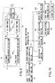
Additionally, by providing a dot recording
prohibiting region 110 having a width equal to the size
of a dot between the block header 28 and the block user
data 30 as shown in FIG. 12, the number of consecutive
black dots over two adjacent blocks can be limited to
a predetermined value without making the boundary of
the block header 28 and the block user data 30 agree
with a partition for modulation codes as shown in
FIG. 4 for either of the two type of modulation code.
Such a dot prohibiting region 110 is effective not only
for this embodiment but also for any embodiments that
use only a single type of modulation code and do not
require switching from one type to another and those
that use more than two types of modulation code.
While the logical structure of the block header 28
and the block user data 30 is not described in detail
above, it may preferably be identical with the one
described in EP 0 713 194 A1 (corresponding to
USSN 08/586,792).
The bit map image of the generated code pattern 26
is then transmitted to the output section 24, which
transforms it into data that can be recognized by a
printing press or a printer and outputs them to the
latter.
Thus, with this embodiment, the modulation codes
generated by either of the two modulation techniques
can be recorded on an optically readable recording
medium in the form of a code pattern without the risk
of reading wrong markers and the error correction
capability or the area occupied by the code pattern can
be determined as a function of the error rate of the
recording medium to optimize the recording efficiency.
[5th Embodiment]
Now, a demodulation method and a demodulator
according to the invention will be described by
referring to the fifth embodiment.
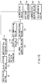
FIG. 13 is a schematic block diagram of a dot code
reproducing apparatus to which the fifth embodiment of
demodulation method and demodulator according to the
invention are applied. The dot code reproducing
apparatus comprises an image pick-up section 46, a
block detecting section 112, a modulation code
extracting section 114, a selecting section 116, a
first demodulating section 118, a bit error correcting
section 120, a second demodulating section 122, a
deinterleaving section 56, a byte error correcting
section 58, a compressed data decoding section 60 and a
data reproducing section 62.
The image pick-up section 46 picks up an optically
readable code pattern and generates a digital image.
The block detecting section 112 detects blocks of dot
codes from the generated digital image and extracts
the black header of each of the detected blocks.
The modulation code extracting section 114 extracts
modulation codes from the block user data and feeds the
modulation switching information of the block header to
the modulation code extracting section 114 and the
selecting section 116.
The modulation code extracting section 114
extracts modulation codes from the block user data in
the block extracted by the block detecting section 112
according to the modulation switching information of
the block header. The selecting section 116 assigns
the modulation codes extracted by the modulation code
extracting section 114 either to the first demodulating
section 118 or to the bit error correcting section 120
according to the modulation switching information.
The first demodulating section 118 generates
demodulation data for the modulation codes assigned
to it by the selecting section 116. The bit error
correcting section 120 corrects bit errors in the
modulation codes assigned to it by the selecting
section 116 and the second demodulating section 122
generates demodulation data for the modulation codes
that have been corrected for bit errors.
The deinterleaving section 56 temporarily stores
the demodulation data generated by the first
demodulating section 118 or the second demodulating
section 122 in an internal memory (not shown) and
rearranges the plurality of pieces of demodulation
data stored in the memory. The byte error correcting
section 58 performs a byte error correcting operation
on the rearranged pieces of demodulation data and the
compressed data decoding section 60 decodes the
compressed data that have been corrected for byte
errors by decompressing them to restore the original
multimedia data in the form of a combination of voice,
image and text. The data reproducing section 62
transforms the restored multimedia data into data that
can be recognized by an output unit (not shown) and
sends them to the output unit.
While it is assumed here that the code pattern has
a configuration as shown in FIG. 2, whereas the
operation of byte error correction is an operation of
correcting Reed-Solomon codes and data are output as
voice data, it should be noted that the present
invention is not limited thereto in any means.
Now, the operation of the fifth embodiment will be
described in detail.
The image pick-up section 46 picks up an image of
the code pattern 26 typically by means of a CCD camera
and binarizes it to produce a binarized image.
The produced binarized image is then entered
to the block detecting section 112, which detects
blocks 36 from the entered binarized image and
determines the positions for reading the block header
28 and the block user data 30. Then, the block address
and the macro block header distribution information
contained in the block header 28 read out at the
determined reading position are transmitted to the
deinterleaving section 56, while the modulation
switching information is transmitted to the modulation
code extracting section 114 and the selecting
section 116. The logical structure of the block
address and that of the macro block header distribution
information are described in detail in EP 0 713 194 A1
(corresponding to USSN 08/586,792) filed by the
applicant of the present patent application and hence
will not be described here.
The modulation code extracting section 114
determines each of the bits read out at the position
for reading the block user data for black or white dot
and transforms them into bit data in order to extract
10- or 13-bit modulation codes according to the bit map
image switching information.
Means for demodulating 10-bit modulation codes
are described in EP 0 765 041 A2 (corresponding to
USSN 08/696,003) filed by the applicant of the present
patent application and means for demodulating 13-bit
modulation codes are described earlier by referring to
the second embodiment.
The selecting section 116 receives the modulation
switching information from the block detecting section
112 and the modulation codes from the modulation code
extracting section 114. The selection section 116
sends the modulation codes to the first demodulating
section when the unequivocally defined modulation
switching information indicates 13-bit modulation
codes (flag "0") and to the bit error correcting
section 120 when the modulation switching information
indicates 13-bit modulation codes (flag "1").
The 13-bit modulation codes subjected to a bit
error correcting operation in the bit error correcting
section 120 are entered to the second demodulating
section 122.
10-bit modulation codes are demodulated to 8-bit
demodulation data in the first demodulating section 118,
whereas 13-bit modulation codes are demodulated to
8-bit demodulation data in the second demodulating
section 122 before they are sent to the deinterleaving
section 56.
The deinterleaving section 56 and the sections
located further downstream operate exactly in a manner
as described by referring to the second embodiment and
hence will not be described here any further.
Thus, with this embodiment, the modulation codes
generated by either of the two modulation techniques
can be recorded on an optically readable recording
medium in the form of a code pattern without the risk
of reading wrong markers and modulation codes of a
specific type can be identified and extracted out
of those of a plurality of different types as a
function of the error rate of the recording medium.
Additionally, when modulation codes are used for a
recording medium showing a high error rate, a
predetermined number of errors generated in the
modulation codes can be corrected in the demodulation
step so that, when combined with the byte error
correcting operation in a subsequent step, the overall
error rate of the data on the recording medium can be
remarkably minimized.
Finally, while the modulation rule is provided
solely in terms of the number of consecutive black dots
to reliably identify markers operating as reference
indexes in the above first through fifth embodiments, a
modulation rule prohibiting the generation of same
black and white patterns for markers 124 operating as
reference indexes as shown in FIG. 14 may alternatively
be used. Still alternatively, a modulation rule
adapted to identify other reading reference patterns
(rectangular patterns, linear patterns or synchronous
clock patterns using dotted lines) that operates as
reference index may also be used.
For the purpose of the invention, the modulation
rule is not limited to providing a limit to the number
of consecutive black dots or exclusion of specific
white and black patterns and may provide, for example,
exclusion of DC components in a manner as popularly
practiced for magnetic recording.
While the invention is described above by
referring to preferred embodiments, it should be
understood that the present invention is not limited to
those embodiments in any means, which may be modified
in various different ways without departing from the
spirit and the scope of the invention. The present
invention can be summarily described as follows.
With this arrangement, since an error correction
checking symbol is added to the modulated digital data
(modulation codes) and the obtained data conforms to a
predetermined modulation rule providing the
adaptability to the related transmission or recording
apparatus, the transmitted or recorded modulation data
can be reliably extracted by a receiving or reproducing
unit, whichever appropriate, and a predetermined number
of errors can be corrected and detected in a simple and
reliable manner out of the errors generated at the time
of reading modulation codes. Thus, the error rate of
the input data to be subjected to an error correcting
operation after the demodulation by a receiving or
reproducing apparatus can be reduced to consequently
reduce the overall error rate and hence make the use of
a transmission and recording medium show a relatively
high error rate feasible.
(2) A method of modulating digital data to be
used for transmitting or recording N-bit data,
characterized by comprising steps of:
inputting an N-bit data; converting the input N-bit data into an M+K-bit
data selected out of a group of L×2M M+K-bit data
(86, 88) according to a predetermined rule, the group
of L×2M M+K-bit data (86, 88) being obtained by adding
K-bit error correction checking symbols generated on
the basis of L error correcting generation polynomials
to M-bit data (N<M) (84) on a one by one basis and in
terms of Hamming distance greater than a predetermined
value; and outputting the converted M+K-bit data.
With this arrangement, since modulation codes are
selected from a group of bit data having respective
error correction checking symbols originating from
different generation polynomials, a modulation rule
that provides an enhanced level of adaptability to the
related transmission or recording apparatus can be used.
Additionally, the transmitted or recorded modulation
data can be reliably extracted by a receiving or
reproducing apparatus, whichever appropriate, and a
predetermined number of errors can be corrected and
detected in a simple and reliable manner out of the
errors generated at the time of reading modulation
codes. Thus, the error rate of the input data to be
subjected to an error correcting operation after the
demodulation by a receiving or reproducing apparatus
can be reduced to consequently reduce the overall error
rate and hence make the use of a transmission and
recording medium show a relatively high error rate
feasible.
(3) A method of modulating digital data to be
used for transmitting or recording N-bit data,
characterized by comprising steps of:
inputting an N-bit data; converting by means of a converting method
selected out of R different converting methods the
input N-bit data into an Mi+Ki-bit data selected out of
a group of 2Mi Mi+Ki-bit data according to a
predetermined rule, the group of 2Mi Mi+Ki-bit data
being obtained by adding Ki-bit error correction
checking symbols (Ki being 0 or a positive integer) to
Mi-bit data (N<M; i=0, 1, 2, 3, ..., R-1) on a one by
one basis; and outputting the converted M+K-bit data along with
information data (106) showing the selected converting
method.
With this arrangement, since error correction
checking symbols with different error correction
capabilities are used to produce a plurality of groups
of modulation codes according a predetermined
modulation rule, it is possible to select a modulation
code conforming to the predetermined modulation rule
that provides adaptability to the related transmission
or recording apparatus, taking the error rate into
consideration. The efficiency of transmission or
recording can be improved by selecting a modulation
code as a function of the error rate of the
transmission or recording medium and the receiving
or reproducing apparatus can reliably extract the
modulation code. Thus, the error rate of the input
data to be subjected to an error correcting operation
after the demodulation by a receiving or reproducing
apparatus can be reduced to consequently reduce the
overall error rate.
(4) The method of modulating digital data
according to one of (1), (2) and (3), characterized in
that the predetermined rule includes one of a rule that
the number of consecutive bits of at least one of "1"s
and "0"s of the modulated digital data shall be less
than the largest number of consecutive bits of the at
least one of "1"s and "0"s constituting the reference
index (32) contained in the digital data to be
transmitted or recorded and a rule that the
predetermined pattern of "1"s and "0"s of the modulated
digital data shall not contain the predetermined
pattern of "1"s and "0"s constituting the reference
indexes (124) contained in the digital data to be
transmitted or recorded.
With this arrangement, a less rigorous limit can
be imposed on the number of selectable modulation codes
and modulation codes can be extracted more reliably at
the time of reception or reproduction to reduce the
number of errors that can be appear at the time of
reading modulation codes if compared with the use of
modulation codes adapted to remove DC components
because the modulation rule provides only
discrimination of modulation codes and reference
indexes (markers). (5) The method of modulating digital data
according to one of (1), (2) and (3), characterized in
that, if the digital data to be transmitted or recorded
comprises a section (28, 30) to be modulated and a
section (34) not to be modulated that are located
adjacent to each other, the predetermined rule includes
one of a rule that the number of consecutive bits of
at least one of "1"s and "0"s of the modulated
digital data shall be less than the largest number of
consecutive bits of the at least one of "1"s and "0"s
constituting the reference index (32) contained in the
digital data to be transmitted or recorded in a region
where the section to be modulated adjoins the section
not to be modulated and a rule that the predetermined
pattern of "1"s and "0"s of the modulated digital data
shall not contain the predetermined pattern of "1"s and
"0"s constituting the reference indexes (124) contained
in the digital data to be transmitted or recorded in a
region where the section to be modulated adjoins the
section not to be modulated.
With this arrangement, a less rigorous limit can
be imposed on the number of selectable modulation codes
and modulation codes can be extracted more reliably at
the time of reception or reproduction to reduce the
number of errors that can be appear at the time of
reading modulation codes if compared with the use of
modulation codes adapted to remove DC components
because the modulation rule provides only
discrimination of modulation codes and reference
indexes (markers), taking into consideration the
section not to be modulated that is located adjacent to
the section to be modulated into consideration. (6) The method of modulating digital data
according to one of (1), (2), (3), (4) and (5),
characterized in that the N-bit data is a data that
corresponds to a 1-byte data at the time of byte error
correction coding to be conducted prior to the
modulation.
With this arrangement, a byte of a byte error
correction code is made to correspond to a modulation
code without increasing the number of byte errors for
wrong corrections that can take place in a demodulation
error correcting operation at the time of reception or
reproduction (error correcting operation on modulation
codes). Thus, the byte error rate can reliably be
reduced in the demodulation error correcting operation
to effectively carry out a byte error correcting
operation after demodulation. (7) A method of demodulating an M+K-bit digital
data obtained by a digital data modulating method of
converting N-bit data into an M+K-bit data selected out
of a group of 2M M+K-bit data according to a
predetermined rule, the group of 2M M+K-bit data being
obtained by adding a K-bit error correction checking
symbol to M-bit data (N<M), back into N-bit data,
characterized by comprising steps of:
carrying out at least one of an error correcting
operation and an error detecting operation on the M+K-bit
data (64); and demodulating the M+K-bit data (66) subjected to
the at least one of the error correcting operation and
the error detecting operation into N-bit data (72).
With this arrangement, demodulation errors can be
reduced or detected by carrying out an error correcting
operation or an error detecting operation on the
modulation code to which an error correction checking
symbol is added. The detected demodulation errors can
be utilized as deletion flags for the error correcting
operation to be conducted after modulation to carry out
the deleting and correcting operation so that the
demodulation errors are reduced or detected to maximize
the error correcting capability for correcting errors
after demodulation.
(8) The method of demodulating digital data
according to (7), characterized in that the step of
demodulating includes steps of:
extracting only the M-bit data (68) from the
M+K-bit data (66) that has been subjected to the at
least one of the error correcting operation and the
error detecting operation by removing the K-bit error
correction checking symbol; and demodulating the extracted M-bit data (68) into an
N-bit data (72).
With this arrangement, demodulation errors can be
reduced or detected by carrying out an error correcting
operation or an error detecting operation on the
modulation codes to which an error correction checking
symbol is added. Additionally, a small demodulation
can be used because the error correction checking
symbol is removed from the modulation code that has
been subjected to an error correcting operation or
an error detecting operation before demodulation.
The detected demodulation errors can be utilized as
deletion flags for the error correcting operation to be
conducted after modulation to carry out the deleting
and correcting operation so that the demodulation
errors are reduced or detected to maximize the error
correcting capability for correcting errors after
demodulation.
(9) A method of demodulating an M+K-bit digital
data obtained by a digital data modulating method of
converting the input N-bit into an M+K-bit data
selected out of a group of L×2M M+K-bit data according
to a predetermined rule, the group of L×2M M+K-bit data
being obtained by adding K-bit error correction
checking symbols generated on the basis of L error
correcting generation polynomials to M-bit data (N<M)
on a one by one basis and in terms of Hamming distance
greater than a predetermined value, into an N-bit data,
characterized by comprising steps of:
carrying out one of an error correcting operation
and an error detecting operation on the M+K-bit data
corresponding to each of the L error correction
generation polynomials; demodulating the L M+K-bit data subjected to the
one of the error correcting operation and the error
detecting operation into L N-bit data; and selecting the most likely N-bit data out of the
demodulated L N-bit data and outputting it with the
demodulation error identifying information
corresponding to the selected N-bit data.
With this arrangement, demodulation errors can be
reduced or detected by carrying out an error correcting
operation or an error detecting operation on the
modulation code to which an error correction checking
symbol is added. The detected demodulation errors can
be utilized as deletion flags for the error correcting
operation to be conducted after modulation to carry out
the deleting and correcting operation so that the
demodulation errors are reduced or detected to maximize
the error correcting capability for correcting errors
after demodulation.
(10) The method of demodulating digital data
according to (9), characterized in that the step of
demodulating includes steps of:
extracting only the L M-bit data from the L
M+K-bit data that has been subjected to the one of the
error correcting operation and the error detecting
operation by removing the respective K-bit error
correction checking symbols; and demodulating the extracted L M-bit data into L
N-bit data.
With this arrangement, demodulation errors can be
reduced or detected by carrying out an error correcting
operation or an error detecting operation on the
modulation codes to which an error correction checking
symbol is added. Additionally, a small demodulation
can be used because the error correction checking
symbol is removed from the modulation code that has
been subjected to an error correcting operation or
an error detecting operation before demodulation.
The detected demodulation errors can be utilized as
deletion flags for the error correcting operation to be
conducted after modulation to carry out the deleting
and correcting operation so that the demodulation
errors are reduced or detected to maximize the error
correcting capability for correcting errors after
demodulation.
(11) A method of demodulating an Mi+Ki-bit
digital data obtained by a digital data modulating
method of converting by means of a converting method
selected out of R different converting methods the
input N-bit into an Mi+Ki-bit data selected out of
a group of 2Mi Mi+Ki-bit data according to a
predetermined rule, the group of 2Mi Mi+Ki-bit data
being obtained by adding Ki-bit error correction
checking symbols (Ki being 0 or a positive integer) to
Mi-bit data (N<M; i=0, 1, 2, 3, ..., R-1) on a one by
one basis, the digital data modulating method including
a step of outputting the obtained Mi+Ki-bit digital
data along with information data showing the selected
converting method, into an N-bit data, characterized by
comprising steps of:
extracting the information data showing the
selected converting method; extracting the Mi+Ki-bit data according to the
extracted information data; and demodulating the extracted Mi+Ki-bit data into an
N-bit data according to the extracted information data.
With this arrangement, the information describing
the type of the modulation code selected according to
the characteristics of the transmission or recording
medium is extracted prior to demodulation so that the
type of modulation code can be determined without
requiring a complicated process and hence the
modulation code can be extracted and demodulated
reliably according to the type of the modulation code.
(12) The method of demodulating digital data
according to (11), characterized by further comprising
step of conducting one of an error correcting operation
and an error detecting operation on the extracted
Mi+Ki-bit data when the Ki determined unequivocally
from the extracted information data is not equal to 0,
and characterized in that
the step of demodulating includes a step of
demodulating the Mi+Ki-bit data that has been subjected
to the one of the error correcting operation and the
error detecting operation into an N-bit data.
With this arrangement, demodulation errors can be
reduced and detected by carrying out an error
correcting operation or an error detecting operation on
the modulation codes of a plurality of different types
to which an error correction checking symbol is added.
The detected demodulation errors can be utilized as
deletion flags for the error correcting operation to be
conducted after modulation to carry out the deleting
and correcting operation so that the demodulation
errors are reduced or detected to maximize the error
correcting capability for correcting errors after
demodulation.
(13) The method of demodulating digital data
according to (11), characterized by further comprising
step of conducting one of an error correcting operation
and an error detecting operation on the extracted
Mi+Ki-bit data when the Ki determined unequivocally
from the extracted information data is not equal to 0,
and characterized in that
the step of demodulating includes steps of: extracting only the Mi-bit data from the Mi+Ki-bit
data that has been subjected to the one of the error
correcting operation and the error detecting operation
by removing the Ki-bit error correcting checking
symbol; and demodulating the extracted Mi-bit data into an
N-bit data.
With this arrangement, demodulation errors can be
reduced or detected by carrying out an error correcting
operation or an error detecting operation on the
modulation codes of a plurality of different types to
which an error correction checking symbol is added.
Additionally, a small demodulation can be used because
the error correction checking symbol is removed from
the modulation code that has been subjected to an error
correcting operation or an error detecting operation
before demodulation. The detected demodulation errors
can be utilized as deletion flags for the error
correcting operation to be conducted after modulation
to carry out the deleting and correcting operation so
that the demodulation errors are reduced or detected to
maximize the error correcting capability for correcting
errors after demodulation.
(14) The method of demodulating digital data
according to one of (7), (8), (9), (10), (11), (12) and
(13), characterized in that the N-bit data is a data
that corresponds to a 1-byte data at the time of byte
error correction decoding to be conducted subsequent to
the demodulation.
With this arrangement, a byte of a byte error
correction code is made to correspond to a modulation
code without increasing the number of byte errors for
wrong corrections that can take place in a demodulation
error correcting operation at the side of the receiving
or reproducing apparatus. Thus, the byte error rate
can reliably be reduced in the demodulation error
correcting operation to effectively carry out a byte
error correcting operation after demodulation. (15) A digital data modulator to be used for
transmitting or recording N-bit data, characterized by
comprising:
an input terminal for inputting an N-bit data; a converting section (modulation table) for
converting the input N-bit data into an M+K-bit data
(44) selected out of a group of 2M M+K-bit data
according to a predetermined rule, the group of 2M M+K-bit
data being obtained by adding a K-bit error
correction checking symbol (40) to M-bit data (N<M)
(38); and an output terminal for outputting the converted
M+K-bit data.
With this arrangement, since an error correction
checking symbol is added to the modulated digital
data (modulation codes) and the obtained data conforms
to a predetermined modulation rule providing the
adaptability to the related transmission or recording
apparatus, the transmitted or recorded modulation data
can be reliably extracted by a receiving or reproducing
apparatus, whichever appropriate, and a predetermined
number of errors can be corrected and detected in a
simple and reliable manner out of the errors generated
at the time of reading modulation codes. Thus, the
error rate of the input data to be subjected to an
error correcting operation after the demodulation by a
receiving or reproducing apparatus can be reduced to
consequently reduce the overall error rate and hence
make the use of a transmission and recording medium
show a relatively high error rate feasible.
(16) A digital data modulator to be used for
transmitting or recording N-bit data, characterized by
comprising:
an input terminal for inputting an N-bit data; a converting section for converting the input
N-bit data into an M+K-bit data selected out of a
group of L×2M M+K-bit data (86, 88) according to a
predetermined rule, the group of L×2M M+K-bit data
being obtained by adding K-bit error correction
checking symbols generated on the basis of L error
correcting generation polynomials to M-bit data (N<M)
(84) on a one by one basis and in terms of Hamming
distance greater than a predetermined value; and an output terminal for outputting the converted
M+K-bit data.
With this arrangement, since modulation codes are
selected from a group of bit data having respective
error correction checking symbols originating from
different generation polynomials, a modulation rule
that provides an enhanced level of adaptability to the
related transmission or recording apparatus can be used
Additionally, the transmitted or recorded modulation
data can be reliably extracted by a receiving or
reproducing apparatus, whichever appropriate, and a
predetermined number of errors can be corrected and
detected in a simple and reliable manner out of the
errors generated at the time of reading modulation
codes. Thus, the error rate of the input data to be
subjected to an error correcting operation after the
demodulation by a receiving or reproducing apparatus
can be reduced to consequently reduce the overall error
rate and hence make the use of a transmission and
recording medium show a relatively high error rate
feasible.
(17) A digital data modulator to be used for
transmitting or recording N-bit data, characterized by
comprising:
an input terminal for inputting an N-bit data; a converting section for converting by means of a
converting method selected out of R different
converting methods the input N-bit data into an Mi+Ki-bit
data selected out of a group of 2Mi Mi+Ki-bit data
according to a predetermined rule, the group of 2Mi
Mi+Ki-bit data being obtained by adding Ki-bit error
correction checking symbols (Ki= 0, 1, 2, 3, ...) to
Mi-bit data (N<M; i=0, 1, 2, 3, ..., R-1) on a one by
one basis; and an output terminal for outputting the converted
M+K-bit data along with information data (106) showing
the selected converting method.
With this arrangement, since error correction
checking symbols with different error correction
capabilities are used to produce a plurality of
groups of modulation codes according a predetermined
modulation rule, it is possible to select a modulation
code conforming to the predetermined modulation rule
that provides adaptability to the related transmission
or recording apparatus, taking the error rate into
consideration. The efficiency of transmission or
recording can be improved by selecting a modulation
code as a function of the error rate of the
transmission or recording medium and the receiving or
reproducing apparatus can reliably extract the
modulation code. Thus, the error rate of the input
data to be subjected to an error correcting operation
after the demodulation by a receiving or reproducing
apparatus can be reduced to consequently reduce the
overall error rate.
(18) The digital data modulator according to one
of (15), (16) and (17), characterized in that the
predetermined rule includes one of a rule that the
number of consecutive bits of at least one of "1"s and
"0"s of the modulated digital data shall be less than
the largest number of consecutive bits of the at least
one of "1"s and "0"s constituting the reference index
(32) contained in the digital data to be transmitted or
recorded and a rule that the predetermined pattern of
"1"s and "0"s of the modulated digital data shall not
contain the predetermined pattern of "1"s and "0"s
constituting the reference indexes (124) contained in
the digital data to be transmitted or recorded.
With this arrangement, a less rigorous limit can
be imposed on the number of selectable modulation codes
and modulation codes can be extracted more reliably at
the time of reception or reproduction to reduce the
number of errors that can be appear at the time of
reading modulation codes if compared with the use of
modulation codes adapted to remove DC components
because the modulation rule provides only
discrimination of modulation codes and reference
indexes (markers). (19) The digital data modulator according to one
of (15), (16) and (17), if the digital data to be
transmitted or recorded comprises a section (28, 30) to
be modulated and a section (34) not to be modulated
that are located adjacent to each other, the
predetermined rule includes one of a rule that the
number of consecutive bits of at least one of "1"s and
"0"s of the modulated digital data shall be less than
the largest number of consecutive bits of the at least
one of "1"s and "0"s constituting the reference index
(32) contained in the digital data to be transmitted or
recorded in a region where the section to be modulated
adjoins the section not to be modulated and a rule that
the predetermined pattern of "1"s and "0"s of the
modulated digital data shall not contain the
predetermined pattern of "1"s and "0"s constituting the
reference indexes (124) contained in the digital data
to be transmitted or recorded in a region where the
section to be modulated adjoins the section not to be
modulated.
With this arrangement, a less rigorous limit can
be imposed on the number of selectable modulation codes
and modulation codes can be extracted more reliably at
the time of reception or reproduction to reduce the
number of errors that can be appear at the time of
reading modulation codes if compared with the use of
modulation codes adapted to remove DC components
because the modulation rule provides only
discrimination of modulation codes and reference
indexes (markers), taking into consideration the
section not to be modulated that is located adjacent to
the section to be modulated into consideration. (20) The digital data modulator according to one
of (15), (16), (17), (18) and (19), characterized in
that the N-bit data is a data that corresponds to a
1-byte data at the time of byte error correction coding
to be conducted prior to the modulation.
With this arrangement, a byte of a byte error
correction code is made to correspond to a modulation
code without increasing the number of byte errors for
wrong corrections that can take place in a demodulation
error correcting operation at the time of reception or
reproduction (error correcting operation on modulation
codes). Thus, the byte error rate can reliably be
reduced in the demodulation error correcting operation
to effectively carry out a byte error correcting
operation after demodulation. (21) A digital data demodulator for demodulating
an M+K-bit digital data obtained by a digital data
modulating method of converting N-bit data into an M+K-bit
data selected out of a group of 2M M+K-bit data
according to a predetermined rule, the group of 2M M+K-bit
data being obtained by adding a K-bit error
correction checking symbol to M-bit data (N<M), back
into N-bit data, characterized by comprising:
an error correcting section (52; 74) carrying out
at least one of an error correcting operation and an
error detecting operation on the M+K-bit data (64); and a demodulating section (54; 76) for demodulating
the M+K-bit data (66) subjected to the at least one of
the error correcting operation and the error detecting
operation into N-bit data (72).
With this arrangement, demodulation errors can be
reduced or detected by carrying out an error correcting
operation or an error detecting operation on the
modulation code to which an error correction checking
symbol is added. The detected demodulation errors can
be utilized as deletion flags for the error correcting
operation to be conducted after modulation to carry out
the deleting and correcting operation so that the
demodulation errors are reduced or detected to maximize
the error correcting capability for correcting errors
after demodulation.
(22) The digital data demodulator according to
(21), characterized in that the demodulating section
extracts only the M-bit data (68) from the M+K-bit data
(66) that has been subjected to the at least one of the
error correcting operation and the error detecting
operation by removing the K-bit error correction
checking symbol and demodulate the extracted M-bit data
(68) into an N-bit data (72).
With this arrangement, demodulation errors can be
reduced or detected by carrying out an error correcting
operation or an error detecting operation on the
modulation codes to which an error correction checking
symbol is added. Additionally, a small demodulation
can be used because the error correction checking
symbol is removed from the modulation code that has
been subjected to an error correcting operation or
an error detecting operation before demodulation.
The detected demodulation errors can be utilized as
deletion flags for the error correcting operation to be
conducted after modulation to carry out the deleting
and correcting operation so that the demodulation
errors are reduced or detected to maximize the error
correcting capability for correcting errors after
demodulation. (23) A digital data demodulator for demodulating
an M+K-bit digital data obtained by a digital data
modulating method of converting the input N-bit into an
M+K-bit data selected out of a group of L×2M M+K-bit
data according to a predetermined rule, the group of
L×2M M+K-bit data being obtained by adding K-bit error
correction checking symbols generated on the basis of L
error correcting generation polynomials to M-bit data
(N<M) on a one by one basis and in terms of Hamming
distance greater than a predetermined value, into an
N-bit data, characterized by comprising:
an error correcting section (741, 742) for
carrying out one of an error correcting operation and
an error detecting operation on the M+K-bit data
corresponding to each of the L error correction
generation polynomials; a demodulating section (761, 762) for demodulating
the L M+K-bit data subjected to the one of the error
correcting operation and the error detecting operation
into L N-bit data; and an output section (763) for selecting the most
likely N-bit data out of the demodulated L N-bit data
and outputting it with the demodulation error
identifying information corresponding to the selected
N-bit data.
With this arrangement, demodulation errors can be
reduced or detected by carrying out an error correcting
operation or an error detecting operation on the
modulation code to which an error correction checking
symbol is added. The detected demodulation errors can
be utilized as deletion flags for the error correcting
operation to be conducted after modulation to carry out
the deleting and correcting operation so that the
demodulation errors are reduced or detected to maximize
the error correcting capability for correcting errors
after demodulation.
(24) The digital data demodulator according to
(23), characterized in that the demodulating section
extracts only the L M-bit data from the L M+K-bit data
that has been subjected to the one of the error
correcting operation and the error detecting operation
by removing the respective K-bit error correction
checking symbols and demodulates the extracted L M-bit
data into L N-bit data.
With this arrangement, demodulation errors can be
reduced or detected by carrying out an error correcting
operation or an error detecting operation on the
modulation codes to which an error correction checking
symbol is added. Additionally, a small demodulation
can be used because the error correction checking
symbol is removed from the modulation code that has
been subjected to an error correcting operation or an
error detecting operation before demodulation. The
detected demodulation errors can be utilized as
deletion flags for the error correcting operation to be
conducted after modulation to carry out the deleting
and correcting operation so that the demodulation
errors are reduced or detected to maximize the error
correcting capability for correcting errors after
demodulation. (25) A digital data demodulator for demodulating
an Mi+Ki-bit digital data obtained by a digital data
modulating method of converting by means of a
converting method selected out of R different
converting methods the input N-bit into an Mi+Ki-bit
data selected out of a group of 2Mi Mi+Ki-bit data
according to a predetermined rule, the group of 2Mi
Mi+Ki-bit data being obtained by adding Ki-bit error
correction checking symbols (Ki being 0 or a positive
integer) to Mi-bit data (N<M; i=0, 1, 2, 3, ..., R-1)
on a one by one basis, the digital data modulating
method including a step of outputting the obtained
Mi+Ki-bit digital data along with information data
showing the selected converting method, into an N-bit
data, characterized by comprising:
an information data extracting section (112) for
extracting the information data showing the selected
converting method; a bit data extracting section (114) for extracting
the Mi+Ki-bit data according to the extracted
information data; and a demodulating section (116, 118, 120, 122) for
demodulating the extracted Mi+Ki-bit data into an N-bit
data according to the extracted information data,
With this arrangement, the information describing
the type of the modulation code selected according to
the characteristics of the transmission or recording
medium is extracted prior to demodulation so that the
type of modulation code can be determined without
requiring a complicated process and hence the
modulation code can be extracted and demodulated
reliably according to the type of the modulation code.
(26) The digital data demodulator according to
(25), characterized in that the demodulating section
(116, 118, 120, 122) for demodulating the extracted
Mi+Ki-bit data into an N-bit data comprises:
an error correcting section (120) for conducting
one of an error correcting operation and an error
detecting operation on the Mi+Ki-bit data when the Ki
determined unequivocally from the extracted information
data is not equal to 0; and a data demodulating section (118, 122) for
demodulating the Mi+Ki-bit data that has been subjected
to the one of the error correcting operation and the
error detecting operation into an N-bit data.
With this arrangement, demodulation errors can be
reduced and detected by carrying out an error
correcting operation or an error detecting operation on
the modulation codes of a plurality of different types
to which an error correction checking symbol is added.
The detected demodulation errors can be utilized as
deletion flags for the error correcting operation to be
conducted after modulation to carry out the deleting
and correcting operation so that the demodulation
errors are reduced or detected to maximize the error
correcting capability for correcting errors after
demodulation.
(27) The digital data demodulator according to
(25), characterized in that the demodulating section
(116, 118, 120, 122) for demodulating the extracted
Mi+Ki-bit data into an N-bit data comprises:
an error correcting section (120) for conducting
one of an error correcting operation and an error
detecting operation on the extracted Mi+Ki-bit data
when the Ki determined unequivocally from the extracted
information data is not equal to 0; a removing section (118, 122) for extracting
only the Mi-bit data from the Mi+Ki-bit data that has
been subjected to the one of the error correcting
operation and the error detecting operation by removing
the Ki-bit error correcting checking symbol; and an extracted data demodulating section (118, 122)
for demodulating the Mi-bit data extracted by the
removing section into an N-bit data.
With this arrangement, demodulation errors can be
reduced or detected by carrying out an error correcting
operation or an error detecting operation on the
modulation codes of a plurality of different types to
which an error correction checking symbol is added.
Additionally, a small demodulation can be used because
the error correction checking symbol is removed from
the modulation code that has been subjected to an error
correcting operation or an error detecting operation
before demodulation. The detected demodulation errors
can be utilized as deletion flags for the error
correcting operation to be conducted after modulation
to carry out the deleting and correcting operation so
that the demodulation errors are reduced or detected to
maximize the error correcting capability for correcting
errors after demodulation.
(28) The digital data demodulator according to
one of (21), (22), (23), (24), (25), (26) and (27),
characterized in that the N-bit data is a data that
corresponds to a 1-byte data at the time of byte error
correction decoding to be conducted subsequent to the
demodulation.
With this arrangement, a byte of a byte error
correction code is made to correspond to a modulation
code without increasing the number of byte errors for
wrong corrections that can take place in a demodulation
error correcting operation at the side of the receiving
or reproducing apparatus. Thus, the byte error rate
can reliably be reduced in the demodulation error
correcting operation to effectively carry out a byte
error correcting operation after demodulation. (29) A method of modulating digital data to be
used for printing and recording an N-bit data on a
predetermined medium as optically readable code pattern,
characterized in that
the code pattern (26) is formed by arranging a
plurality of blocks (36) having a predetermined area
adapted to hold a predetermined volume of data, the
block at least comprising: a pattern (30) formed by a
plurality of dot images arranged in correspondence with
the held data; a marker (32; 124) arranged with a
predetermined positional relationship with the dot
image pattern to determine a reference position for
reading the dot image pattern; and a block address
pattern (28) for indicating the positions of the blocks
of the code pattern and, when an N-bit data is converted into an M-bit
data selected out of a group of 2M M-bit data (N<M)
according to a predetermined rule and data values of
the M-bit data are caused to correspond to respective
dot images of predetermined colors, the total number of
dot images contained in each of the blocks is made
equal to a value obtained by multiplying the M by an
integer.
With this arrangement, in an operation of
recording a modulation code as a code pattern of blocks,
the number of recordable dot images of each block is
made equal to a value obtained by multiplying the
number of modulation code bits by an integer in order
to prevent the modulation code from being recorded over
two blocks so that it can be read out randomly on a
block by block basis. Thus, the operation of manually
scanning and reading a code pattern can be carried out
with less restrictions.
(30) The method of modulating digital data
according to (29), characterized in that the total
number of dot images contained at least one of the
blocks is made equal to a value obtained by multiplying
the M by an integer by making the block contain a
number of dot images of dummy data.
With this arrangement, in an operation of
recording a modulation code as a code pattern of blocks,
the number of recordable dot images of each block is
made equal to a value obtained by multiplying the
number of modulation code bits by an integer by adding
dummy data in order to prevent the modulation code from
being recorded over two blocks so that it can be read
out randomly on a block by block basis. Thus, the
operation of manually scanning and reading a code
pattern can be carried out with less restrictions.