EP0867773A2 - Stage apparatus and method for producing circuit device utilizing the same - Google Patents
Stage apparatus and method for producing circuit device utilizing the same Download PDFInfo
- Publication number
- EP0867773A2 EP0867773A2 EP98302173A EP98302173A EP0867773A2 EP 0867773 A2 EP0867773 A2 EP 0867773A2 EP 98302173 A EP98302173 A EP 98302173A EP 98302173 A EP98302173 A EP 98302173A EP 0867773 A2 EP0867773 A2 EP 0867773A2
- Authority
- EP
- European Patent Office
- Prior art keywords
- structure body
- stage structure
- substrate plate
- adsorption
- stage
- Prior art date
- Legal status (The legal status is an assumption and is not a legal conclusion. Google has not performed a legal analysis and makes no representation as to the accuracy of the status listed.)
- Granted
Links
- 238000004519 manufacturing process Methods 0.000 title claims description 8
- 238000001179 sorption measurement Methods 0.000 claims abstract description 295
- 230000009471 action Effects 0.000 claims abstract description 181
- 230000002459 sustained effect Effects 0.000 claims abstract description 10
- 230000005611 electricity Effects 0.000 claims abstract description 8
- 239000000758 substrate Substances 0.000 claims description 194
- 239000012530 fluid Substances 0.000 claims description 156
- 230000007246 mechanism Effects 0.000 claims description 97
- 238000012545 processing Methods 0.000 claims description 94
- 238000000034 method Methods 0.000 claims description 89
- 230000008569 process Effects 0.000 claims description 68
- 238000012546 transfer Methods 0.000 claims description 51
- 230000033001 locomotion Effects 0.000 claims description 47
- 238000004891 communication Methods 0.000 claims description 37
- 238000009825 accumulation Methods 0.000 claims description 32
- 238000012544 monitoring process Methods 0.000 claims description 31
- 230000003287 optical effect Effects 0.000 claims description 30
- 230000004044 response Effects 0.000 claims description 30
- 230000006870 function Effects 0.000 claims description 29
- 230000002829 reductive effect Effects 0.000 claims description 28
- 238000001459 lithography Methods 0.000 claims description 23
- 238000005286 illumination Methods 0.000 claims description 20
- 239000004065 semiconductor Substances 0.000 claims description 17
- 230000000903 blocking effect Effects 0.000 claims description 15
- 238000007667 floating Methods 0.000 claims description 12
- 238000001514 detection method Methods 0.000 claims description 11
- 230000003578 releasing effect Effects 0.000 claims description 10
- 230000009466 transformation Effects 0.000 claims description 9
- 239000004973 liquid crystal related substance Substances 0.000 claims description 5
- 239000013589 supplement Substances 0.000 claims description 5
- 230000009467 reduction Effects 0.000 claims description 4
- 229910010293 ceramic material Inorganic materials 0.000 claims description 3
- 238000007689 inspection Methods 0.000 claims 4
- 238000013518 transcription Methods 0.000 claims 4
- 230000035897 transcription Effects 0.000 claims 4
- 238000003825 pressing Methods 0.000 claims 1
- 235000012431 wafers Nutrition 0.000 abstract description 433
- 230000003068 static effect Effects 0.000 abstract description 8
- 238000009429 electrical wiring Methods 0.000 abstract description 5
- 230000007935 neutral effect Effects 0.000 description 14
- 239000000463 material Substances 0.000 description 12
- 229910052751 metal Inorganic materials 0.000 description 11
- 239000002184 metal Substances 0.000 description 11
- 230000008901 benefit Effects 0.000 description 9
- 230000000694 effects Effects 0.000 description 9
- 238000012986 modification Methods 0.000 description 9
- 230000004048 modification Effects 0.000 description 9
- 230000001133 acceleration Effects 0.000 description 7
- 238000004458 analytical method Methods 0.000 description 7
- 239000000919 ceramic Substances 0.000 description 7
- 239000007789 gas Substances 0.000 description 7
- 238000005259 measurement Methods 0.000 description 7
- 238000010586 diagram Methods 0.000 description 6
- 238000005516 engineering process Methods 0.000 description 6
- 230000008859 change Effects 0.000 description 5
- 230000036961 partial effect Effects 0.000 description 5
- 230000005856 abnormality Effects 0.000 description 4
- OJIJEKBXJYRIBZ-UHFFFAOYSA-N cadmium nickel Chemical compound [Ni].[Cd] OJIJEKBXJYRIBZ-UHFFFAOYSA-N 0.000 description 4
- 239000011521 glass Substances 0.000 description 4
- 238000007726 management method Methods 0.000 description 4
- 238000012790 confirmation Methods 0.000 description 3
- 230000006866 deterioration Effects 0.000 description 3
- 230000002542 deteriorative effect Effects 0.000 description 3
- 238000007599 discharging Methods 0.000 description 3
- 238000009826 distribution Methods 0.000 description 3
- 238000010894 electron beam technology Methods 0.000 description 3
- 238000003780 insertion Methods 0.000 description 3
- 230000037431 insertion Effects 0.000 description 3
- 239000002245 particle Substances 0.000 description 3
- 230000002093 peripheral effect Effects 0.000 description 3
- 239000004033 plastic Substances 0.000 description 3
- 229920003023 plastic Polymers 0.000 description 3
- 239000007787 solid Substances 0.000 description 3
- 208000019901 Anxiety disease Diseases 0.000 description 2
- IJGRMHOSHXDMSA-UHFFFAOYSA-N Atomic nitrogen Chemical compound N#N IJGRMHOSHXDMSA-UHFFFAOYSA-N 0.000 description 2
- 230000002159 abnormal effect Effects 0.000 description 2
- 238000010521 absorption reaction Methods 0.000 description 2
- 230000002411 adverse Effects 0.000 description 2
- 238000004378 air conditioning Methods 0.000 description 2
- 230000036506 anxiety Effects 0.000 description 2
- 230000003247 decreasing effect Effects 0.000 description 2
- 238000006073 displacement reaction Methods 0.000 description 2
- 239000010419 fine particle Substances 0.000 description 2
- 238000011065 in-situ storage Methods 0.000 description 2
- 239000011261 inert gas Substances 0.000 description 2
- 230000000977 initiatory effect Effects 0.000 description 2
- 238000012423 maintenance Methods 0.000 description 2
- 230000010355 oscillation Effects 0.000 description 2
- 230000003252 repetitive effect Effects 0.000 description 2
- 230000004043 responsiveness Effects 0.000 description 2
- 230000002441 reversible effect Effects 0.000 description 2
- CBENFWSGALASAD-UHFFFAOYSA-N Ozone Chemical compound [O-][O+]=O CBENFWSGALASAD-UHFFFAOYSA-N 0.000 description 1
- 230000004075 alteration Effects 0.000 description 1
- 229910052782 aluminium Inorganic materials 0.000 description 1
- XAGFODPZIPBFFR-UHFFFAOYSA-N aluminium Chemical compound [Al] XAGFODPZIPBFFR-UHFFFAOYSA-N 0.000 description 1
- 230000003321 amplification Effects 0.000 description 1
- 230000003466 anti-cipated effect Effects 0.000 description 1
- 238000013459 approach Methods 0.000 description 1
- QVGXLLKOCUKJST-UHFFFAOYSA-N atomic oxygen Chemical compound [O] QVGXLLKOCUKJST-UHFFFAOYSA-N 0.000 description 1
- 230000033228 biological regulation Effects 0.000 description 1
- 238000007664 blowing Methods 0.000 description 1
- 239000003990 capacitor Substances 0.000 description 1
- 238000006243 chemical reaction Methods 0.000 description 1
- 239000011248 coating agent Substances 0.000 description 1
- 238000000576 coating method Methods 0.000 description 1
- 230000006835 compression Effects 0.000 description 1
- 238000007906 compression Methods 0.000 description 1
- 238000012937 correction Methods 0.000 description 1
- 238000005520 cutting process Methods 0.000 description 1
- 239000013013 elastic material Substances 0.000 description 1
- 230000002708 enhancing effect Effects 0.000 description 1
- 230000004438 eyesight Effects 0.000 description 1
- 230000002349 favourable effect Effects 0.000 description 1
- 239000004519 grease Substances 0.000 description 1
- 239000001307 helium Substances 0.000 description 1
- 229910052734 helium Inorganic materials 0.000 description 1
- SWQJXJOGLNCZEY-UHFFFAOYSA-N helium atom Chemical compound [He] SWQJXJOGLNCZEY-UHFFFAOYSA-N 0.000 description 1
- 239000001257 hydrogen Substances 0.000 description 1
- 229910052739 hydrogen Inorganic materials 0.000 description 1
- 230000006872 improvement Effects 0.000 description 1
- 238000009413 insulation Methods 0.000 description 1
- 238000011835 investigation Methods 0.000 description 1
- 238000011031 large-scale manufacturing process Methods 0.000 description 1
- 239000000696 magnetic material Substances 0.000 description 1
- 239000011159 matrix material Substances 0.000 description 1
- 230000003340 mental effect Effects 0.000 description 1
- QSHDDOUJBYECFT-UHFFFAOYSA-N mercury Chemical compound [Hg] QSHDDOUJBYECFT-UHFFFAOYSA-N 0.000 description 1
- 229910052753 mercury Inorganic materials 0.000 description 1
- 229910052757 nitrogen Inorganic materials 0.000 description 1
- 238000003199 nucleic acid amplification method Methods 0.000 description 1
- 239000013307 optical fiber Substances 0.000 description 1
- 239000001301 oxygen Substances 0.000 description 1
- 229910052760 oxygen Inorganic materials 0.000 description 1
- 238000012856 packing Methods 0.000 description 1
- 229920002120 photoresistant polymer Polymers 0.000 description 1
- 238000002360 preparation method Methods 0.000 description 1
- 230000005855 radiation Effects 0.000 description 1
- 230000001846 repelling effect Effects 0.000 description 1
- 238000005070 sampling Methods 0.000 description 1
- 238000007789 sealing Methods 0.000 description 1
- 238000004092 self-diagnosis Methods 0.000 description 1
- 239000007779 soft material Substances 0.000 description 1
- 230000000087 stabilizing effect Effects 0.000 description 1
- 230000001502 supplementing effect Effects 0.000 description 1
- 239000010409 thin film Substances 0.000 description 1
- 230000007306 turnover Effects 0.000 description 1
- 238000009827 uniform distribution Methods 0.000 description 1
- 230000004304 visual acuity Effects 0.000 description 1
- XLYOFNOQVPJJNP-UHFFFAOYSA-N water Substances O XLYOFNOQVPJJNP-UHFFFAOYSA-N 0.000 description 1
Images


Classifications
-
- G—PHYSICS
- G03—PHOTOGRAPHY; CINEMATOGRAPHY; ANALOGOUS TECHNIQUES USING WAVES OTHER THAN OPTICAL WAVES; ELECTROGRAPHY; HOLOGRAPHY
- G03F—PHOTOMECHANICAL PRODUCTION OF TEXTURED OR PATTERNED SURFACES, e.g. FOR PRINTING, FOR PROCESSING OF SEMICONDUCTOR DEVICES; MATERIALS THEREFOR; ORIGINALS THEREFOR; APPARATUS SPECIALLY ADAPTED THEREFOR
- G03F7/00—Photomechanical, e.g. photolithographic, production of textured or patterned surfaces, e.g. printing surfaces; Materials therefor, e.g. comprising photoresists; Apparatus specially adapted therefor
- G03F7/70—Microphotolithographic exposure; Apparatus therefor
- G03F7/70691—Handling of masks or workpieces
- G03F7/707—Chucks, e.g. chucking or un-chucking operations or structural details
- G03F7/70708—Chucks, e.g. chucking or un-chucking operations or structural details being electrostatic; Electrostatically deformable vacuum chucks
-
- G—PHYSICS
- G03—PHOTOGRAPHY; CINEMATOGRAPHY; ANALOGOUS TECHNIQUES USING WAVES OTHER THAN OPTICAL WAVES; ELECTROGRAPHY; HOLOGRAPHY
- G03F—PHOTOMECHANICAL PRODUCTION OF TEXTURED OR PATTERNED SURFACES, e.g. FOR PRINTING, FOR PROCESSING OF SEMICONDUCTOR DEVICES; MATERIALS THEREFOR; ORIGINALS THEREFOR; APPARATUS SPECIALLY ADAPTED THEREFOR
- G03F7/00—Photomechanical, e.g. photolithographic, production of textured or patterned surfaces, e.g. printing surfaces; Materials therefor, e.g. comprising photoresists; Apparatus specially adapted therefor
- G03F7/70—Microphotolithographic exposure; Apparatus therefor
- G03F7/70216—Mask projection systems
- G03F7/70358—Scanning exposure, i.e. relative movement of patterned beam and workpiece during imaging
-
- G—PHYSICS
- G03—PHOTOGRAPHY; CINEMATOGRAPHY; ANALOGOUS TECHNIQUES USING WAVES OTHER THAN OPTICAL WAVES; ELECTROGRAPHY; HOLOGRAPHY
- G03F—PHOTOMECHANICAL PRODUCTION OF TEXTURED OR PATTERNED SURFACES, e.g. FOR PRINTING, FOR PROCESSING OF SEMICONDUCTOR DEVICES; MATERIALS THEREFOR; ORIGINALS THEREFOR; APPARATUS SPECIALLY ADAPTED THEREFOR
- G03F7/00—Photomechanical, e.g. photolithographic, production of textured or patterned surfaces, e.g. printing surfaces; Materials therefor, e.g. comprising photoresists; Apparatus specially adapted therefor
- G03F7/70—Microphotolithographic exposure; Apparatus therefor
- G03F7/70691—Handling of masks or workpieces
- G03F7/707—Chucks, e.g. chucking or un-chucking operations or structural details
-
- G—PHYSICS
- G03—PHOTOGRAPHY; CINEMATOGRAPHY; ANALOGOUS TECHNIQUES USING WAVES OTHER THAN OPTICAL WAVES; ELECTROGRAPHY; HOLOGRAPHY
- G03F—PHOTOMECHANICAL PRODUCTION OF TEXTURED OR PATTERNED SURFACES, e.g. FOR PRINTING, FOR PROCESSING OF SEMICONDUCTOR DEVICES; MATERIALS THEREFOR; ORIGINALS THEREFOR; APPARATUS SPECIALLY ADAPTED THEREFOR
- G03F7/00—Photomechanical, e.g. photolithographic, production of textured or patterned surfaces, e.g. printing surfaces; Materials therefor, e.g. comprising photoresists; Apparatus specially adapted therefor
- G03F7/70—Microphotolithographic exposure; Apparatus therefor
- G03F7/70691—Handling of masks or workpieces
- G03F7/70716—Stages
-
- G—PHYSICS
- G03—PHOTOGRAPHY; CINEMATOGRAPHY; ANALOGOUS TECHNIQUES USING WAVES OTHER THAN OPTICAL WAVES; ELECTROGRAPHY; HOLOGRAPHY
- G03F—PHOTOMECHANICAL PRODUCTION OF TEXTURED OR PATTERNED SURFACES, e.g. FOR PRINTING, FOR PROCESSING OF SEMICONDUCTOR DEVICES; MATERIALS THEREFOR; ORIGINALS THEREFOR; APPARATUS SPECIALLY ADAPTED THEREFOR
- G03F7/00—Photomechanical, e.g. photolithographic, production of textured or patterned surfaces, e.g. printing surfaces; Materials therefor, e.g. comprising photoresists; Apparatus specially adapted therefor
- G03F7/70—Microphotolithographic exposure; Apparatus therefor
- G03F7/708—Construction of apparatus, e.g. environment aspects, hygiene aspects or materials
- G03F7/70991—Connection with other apparatus, e.g. multiple exposure stations, particular arrangement of exposure apparatus and pre-exposure and/or post-exposure apparatus; Shared apparatus, e.g. having shared radiation source, shared mask or workpiece stage, shared base-plate; Utilities, e.g. cable, pipe or wireless arrangements for data, power, fluids or vacuum
-
- H—ELECTRICITY
- H01—ELECTRIC ELEMENTS
- H01L—SEMICONDUCTOR DEVICES NOT COVERED BY CLASS H10
- H01L21/00—Processes or apparatus adapted for the manufacture or treatment of semiconductor or solid state devices or of parts thereof
- H01L21/67—Apparatus specially adapted for handling semiconductor or electric solid state devices during manufacture or treatment thereof; Apparatus specially adapted for handling wafers during manufacture or treatment of semiconductor or electric solid state devices or components ; Apparatus not specifically provided for elsewhere
- H01L21/68—Apparatus specially adapted for handling semiconductor or electric solid state devices during manufacture or treatment thereof; Apparatus specially adapted for handling wafers during manufacture or treatment of semiconductor or electric solid state devices or components ; Apparatus not specifically provided for elsewhere for positioning, orientation or alignment
-
- H—ELECTRICITY
- H01—ELECTRIC ELEMENTS
- H01L—SEMICONDUCTOR DEVICES NOT COVERED BY CLASS H10
- H01L21/00—Processes or apparatus adapted for the manufacture or treatment of semiconductor or solid state devices or of parts thereof
- H01L21/67—Apparatus specially adapted for handling semiconductor or electric solid state devices during manufacture or treatment thereof; Apparatus specially adapted for handling wafers during manufacture or treatment of semiconductor or electric solid state devices or components ; Apparatus not specifically provided for elsewhere
- H01L21/683—Apparatus specially adapted for handling semiconductor or electric solid state devices during manufacture or treatment thereof; Apparatus specially adapted for handling wafers during manufacture or treatment of semiconductor or electric solid state devices or components ; Apparatus not specifically provided for elsewhere for supporting or gripping
- H01L21/6838—Apparatus specially adapted for handling semiconductor or electric solid state devices during manufacture or treatment thereof; Apparatus specially adapted for handling wafers during manufacture or treatment of semiconductor or electric solid state devices or components ; Apparatus not specifically provided for elsewhere for supporting or gripping with gripping and holding devices using a vacuum; Bernoulli devices
Definitions
- the present invention relates to a high-precision transfer stage apparatus for use with lithography apparatuses, instrument apparatuses or other apparatuses and a method for producing circuit patterns utilizing the same and, more particularly, to a stage apparatus for use with an exposure apparatus to be used in a lithography process for producing particularly semiconductor devices and liquid crystal display devices and a method for forming device patterns on a photosensitive substrate plate using such an exposure apparatus.
- a variety of exposure apparatuses have been employed in situ in a lithography process for producing semiconductor devices.
- a compression projection exposure apparatus (usually called a stepper) of a step-and-repeat system is employed predominantly.
- a projection exposure apparatus in a step-and-scan system so arranged as to scan a mask with a circuit pattern drawn as an original picture thereon and a photosensitive substrate plate (a semiconductor wafer) for producing devices relative to an optical projection system
- a X-rays stepper so arranged as to set a mask and a photosensitive substrate plate at a given gap interval and to expose the mask and the photosensitive substrate plate to X-rays such as SOR rays in a step-and-repeat system
- a electron beams exposure apparatus for drawing a circuit pattern with charged particle beams or transcribing a mask by radiation of electron beams, etc.
- a transfer stage apparatus which is so arranged as to hold a photosensitive or sensitive substrate plate (e.g., a semiconductor wafer with a photoresist layer coated thereon) and to move in a two-dimensional direction with respect to a pattern projection system (e.g., a projection system of a pattern image or the mask itself, etc.).
- a pattern projection system e.g., a projection system of a pattern image or the mask itself, etc.
- stage apparatus of a type in which a movable main stage member is held on a guide plane of a base table with a needle bearing or an air bearing and it is transferred by a drive source of a contact type using a feed screw and a nut, etc., or of a non-contact type using a combination of plural linear motors, etc.
- the such stage apparatuses are connected each to plural flexible tubes for supplying vacuum pressure or pressure-applying fluid to a holder of a vacuum adsorption system for holding and adsorbing a substrate plate or an aerodynamic operation source (e.g., piston, vacuum pad part, etc.). Therefore, the movable main stage member is transferred while dragging those flexible tubes from the base table.
- the movable main stage member is provided with various electrical drive sources (e.g., rotary motor, voice coil motor, piezo element, electromagnet, etc.). To those electrical drive sources are connected plural electrical wiring for supplying electrical energy from the base table side or an apparatus column side. Thus, the movable main stage member is transferred while dragging such wiring.
- the plural linear motors are subjected to servo control so as for a measured value of a predetermined position of the coordinates of the movable main stage member measured by a laser interferometer to be present within a predetermined error scope (e.g. ⁇ 0.04 ⁇ m) with respect to the instructed target position.
- a predetermined error scope e.g. ⁇ 0.04 ⁇ m
- the main stage member is subjected to servo control, including a variation in a force (tension) caused by pulling the flexible tubes or electrical wires, a vibration of the tubes or the wiring themselves, etc., as a consequence worsening performance in transferring at a equal speed and in stopping in a predetermined position with a high degree of precision from a desired specification.
- the movable main stage member is made lightweight by using a honeycomb (hollow) structure of a ceramics material in order to raise responsiveness to frequency of the movable main stage member
- various vibrations including a vibration of a power source in an air-conditioning chamber and an air vibration (sound wave) by blowing air from the air-conditioning chamber may be likely to be transmitted through the flexible tubes and the electrical wiring, thereby adversely affecting the dynamic and static features of the main stage member.
- they may cause deteriorating in precision of the position for transcribing circuit patterns to be formed on the substrate plate, in a resolving power thereof, and in precision of superimposition thereof.
- a servo feature unlikely to undergo an influence of tension of the tubes and the wiring as well as various vibrations can be achieved by making an output capacity of various drive actuators (motors, electromagnets, etc.) for driving the movable main stage member in the directions X, Y (and Z, ⁇ ) remarkably strong and making a loop gain great at the time of the servo control.
- various drive actuators motors, electromagnets, etc.
- the stronger output capacity of the drive source may increase an exothermic amount, thereby causing a fluctuation of temperature in the air within a light path of the laser interferometer and a variation in reflectance, leading to deterioration in a precision of length measurement.
- the primary object of the present invention is to provide a stage apparatus so adapted as to prevent deterioration in dynamic and static features due to an influence of various tubes and wiring connected to a movable main stage member of the stage apparatus.
- the present invention has a second object to provide a stage apparatus with a tube excluded therefrom, which otherwise is connected to a movable stage with a function of adsorbing a substrate plate via vacuum pressure in an exchangeable manner by supplying a pressure-reducing fluid (vacuum pressure) thereto.
- the present invention has a third object to provide a lithography exposure apparatus with the such stage apparatus loaded thereon for exposing a circuit device for a semiconductor element or a liquid crystal display element and a method for producing a circuit pattern (a device pattern) by utilizing an improved operation method of the such exposure apparatus.
- the present invention is applied to a transfer stage apparatus having a base structure body (e.g. a base table, etc.), a stage structure body (e.g. a movable main stage member, etc.) disposed so as to be movable in and along a predetermined plane (XY-plane) defined by the base structure body, and a substrate plate-loading part (e.g. a holder, etc) for holding a processing substrate plate (e.g. a wafer, etc.) on the stage structure body.
- a base structure body e.g. a base table, etc.
- a stage structure body e.g. a movable main stage member, etc.
- a substrate plate-loading part e.g. a holder, etc
- the movable stage apparatus is provided with an electrical drive unit (e.g. a group of an electromagnetic drive unit and a permanent magnet, etc.) for transferring the stage structure body in a non-contact system along a predetermined flat plane (a defined flat plane) of the base structure body in a state floating from the base structure body; an electrical adsorption unit (e.g. an electrode for electrostatic adsorption, etc.) for adsorbing the processing substrate plate on the substrate plate-loading part; a re-chargeable battery (e.g. nickel-cadmium battery, etc.) for accumulating electrical energy disposed in the stage structure body; a feed control circuit (e.g.
- CPU high voltage control circuit, drive circuit, etc.
- a receiving circuit e.g. RFC, a digital converter circuit or a feed terminal part and a data coupler part, etc.
- the present invention is applied to the transfer stage apparatus having a base structure body (e.g. a base table, etc.), a stage structure body (e.g. a movable main stage member, etc.) disposed so as to be movable in or along a predetermined plane (XY-plane) defined by the base structure body, and a substrate plate-loading part (e.g. a holder, etc) for holding a processing substrate plate (e.g. a wafer, etc.) on the stage structure body, in which the transfer stage apparatus is further provided with an electrostatic adsorption unit (e.g.
- an electrode, etc. for electrostatically adsorbing the processing substrate plate on the substrate plate-loading part; a re-chargeable battery (e.g. nickel-cadmium battery, etc.) disposed in the stage structure body; a feed control circuit (e.g. CPU, high voltage control circuit, etc.) for controlling electrical energy from the battery and supplying the electrical energy to the electrostatic adsorption unit disposed in the stage structure body; and a receiving circuit (e.g. FRC, a digital converter circuit or a feed terminal part and a data coupler part, etc.) for receiving control information for giving an instruction of an action of the feed control circuit disposed in the stage structure body.
- a feed control circuit e.g. CPU, high voltage control circuit, etc.
- a receiving circuit e.g. FRC, a digital converter circuit or a feed terminal part and a data coupler part, etc.
- the present invention is applied to a method for producing a circuit device on a processing substrate plate by the step of transferring a movable stage structure body (e.g. a movable main stage member, etc.) on a base structure body (e.g. a base table, etc.) in accordance with a control program stored in advance (e.g. stored in a minicomputer or a control unit board, etc.) and the step of transcribing a circuit pattern on each of plural sheets of processing substrate plates (e.g. wafers, etc.) loaded on the stage structure body so as to be exchangeable.
- a control program stored in advance e.g. stored in a minicomputer or a control unit board, etc.
- the stage structure body is provided with a rechargeable battery (e.g. nickel-cadmium battery, etc.) for supplying electrical energy to at least one of a first actuator (e.g. a holder and an electrode on the surface thereof, etc.) for adsorbing and fixing the processing substrate plate on the stage structure body and a second actuator (e.g. a motor for minute motion, etc.) for minutely transferring the processing substrate plate on the stage structure body with three freedoms or more and with an electrical receipt edge orifice (e.g. a receipt terminal part, etc.) for charging the battery, the base structure body is provided with a feed edge orifice (e.g.
- a feed terminal part, etc. for sending a charging electric current to the battery upon connection to the receipt edge orifice when the stage structure body is located in a predetermined standby position (e.g. a loading position, etc.); and a command or parameter for transferring the stage structure body to the standby position for charging the battery is made registrable as a portion of a control program at an appropriate point of time during a period of time during which the plural sheets of processing substrate plates are being processed.
- the present invention is applied to the transfer stage apparatus having a base structure body (e.g. a base table, a column, etc.) and a stage structure body (e.g. a main stage member, etc.) moving along a predetermined plane (XY-plane) defined by the base structure body and forming at a portion thereof with a loading surface (e.g. a holder, etc.) for adsorbing a processing substrate plate (e.g.
- the stage apparatus further comprises a feed edge orifice disposed at a portion of the base structure body for sending a negative pressure fluid for adsorbing the processing substrate plate on the loading surface of the stage structure body; a receipt edge orifice for receiving the negative pressure fluid on the stage structure body side, which is disposed at a portion of the stage structure body so as to be engageable with the feed edge orifice when the stage structure body is transferred to a predetermined waiting position (e.g.
- a valve mechanism for opening or closing a path of the negative pressure fluid, extending between the feed edge orifice and the loading surface of the stage structure body; and a control unit for bringing the valve mechanism into an open state during engagement of the feed edge orifice with the receipt edge orifice when the stage structure body is transferred to the waiting position and for bringing the valve mechanism into a closed state during non-engagement of the feed edge orifice with the receipt edge orifice.
- the present invention can be further applied to a transfer stage apparatus having a base structure body and a stage structure body moving along a predetermined plane (XY-plane) defined by the base structure body and forming at its portion with a loading surface (e.g. a holder, etc.) adsorbing a processing substrate plate under reduced pressure
- the stage apparatus further comprises a sending mechanism disposed at a portion of the base structure body for sending a negative pressure fluid to the loading surface of the stage structure body for adsorbing a processing substrate plate; and a receiving mechanism. disposed at a portion of the stage structure body so as to be engaged with the feed mechanism when the stage structure body is located in a predetermined waiting position (e.g. a loading position, etc.), for leading the negative pressure fluid from the feed mechanism to the loading surface of the stage structure body during engagement with the feed mechanism and for blocking communication with open air during non-engagement with the feed mechanism.
- a predetermined waiting position e.g. a loading position, etc.
- the present invention can be applied to a method for forming an image of a circuit pattern on an exposing substrate plate using a projection exposure apparatus having a first stage structure body movable at least one-dimensionally upon scanning exposure while adsorbing and holding a mask substrate plate with the circuit pattern formed thereon and a second stage structure body movable at least one-dimensionally upon scanning exposure while adsorbing and holding the exposing substrate plate.
- the present invention is practiced by executing the step of loading a first accumulation member (e.g. battery, a tank chamber, etc.) on the first stage structure body (e.g. a reticle stage, etc.), the first accumulation member being for accumulating energy (e.g. electricity for electrostatic adsorption or a pressure-reducing fluid for vacuum adsorption, etc.) necessary for sustaining the adsorption of a mask substrate plate (e.g. a reticle, etc.) over a predetermined period of time on the first stage structure body, and sustaining a self-sustaining adsorption of the mask substrate plate by energy from the first accumulation member (e.g.
- a first accumulation member e.g. battery, a tank chamber, etc.
- the first accumulation member being for accumulating energy (e.g. electricity for electrostatic adsorption or a pressure-reducing fluid for vacuum adsorption, etc.) necessary for sustaining the adsorption of a mask substrate plate (e.g. a reti
- a new energy e.g. electricity, pressure-reducing fluid, etc.
- a new energy e.g. electricity, pressure-reducing fluid, etc.
- the second accumulation member being for accumulating energy
- the present invention can further be applied to a method for producing a circuit device on a processing substrate plate using a lithography apparatus in which the processing substrate plate is held on a stage structure body (e.g. a movable main stage member, etc.) transferring on a base structure body and a desired circuit pattern is exposed to the processing substrate plate by transferring the stage structure body.
- a stage structure body e.g. a movable main stage member, etc.
- the present invention is practiced by the step of carrying the processing substrate plate toward a predetermined loading position (e.g. the wafer exchanging position, etc.) defined on the base structure body and transferring the stage structure body to the loading position; the step of delivering the processing substrate plate onto a substrate plate-loading part (e.g. a holder, etc.) of the stage structure body in the loading position; the step of supplying a pressure-reducing fluid or a pressure-applying fluid to a closed space part (e.g.
- the present invention is based on the basic concept that the number of the tubes and wiring is decreased to the least possible number in order to decrease an influence caused by the tension of the tubes and the wiring to be connected otherwise to the movable main stage member.
- the stage apparatus is configured in such a manner that a vacuum operation source (e.g. a wafer or a holder with a mask adsorbed thereon, etc.) disposed in the movable main stage member or an aerodynamic operation source (e.g. an air bearing for floating, etc.) is replaced with an electrical operation source by an electromagnetic force or an electrostatic force and the electrical energy for operating the electrical operation source as well as the electrical operation source (e.g. a coil of a linear motor, etc.) for transferring the movable main stage member is supplied through a drive circuit from a battery loaded on the movable main stage member and further that the drive circuit is controlled in a wireless system by electric radio or optical communications.
- a vacuum operation source e.g. a wafer or a holder with a mask
- At least a flexible tube for supplying vacuum pressure or compressed air is not needed by replacing the vacuum operation source or the aerodynamic operation source in the movable main stage member is replaced with the electrical operation source.
- a bundle of large wire lines for supplying electric power is not needed by loading the battery and the drive circuit on the movable main stage member. In this mode, therefore, only a fine cable for communications is connected to the drive circuit, thereby making the tension of the cables added to the movable main stage member smaller.
- the stage apparatus in another mode of the present invention, only a flexible tube for supplying vacuum pressure or compressed air is not used and the electrical energy is supplied by a wire line as usual.
- the battery loaded on the movable main stage member is used for feeding electrical energy to an adsorption operation source by electrostatic energy or a small-size motor having a low consumption of electric power, while an electromagnetic actuator having a large electric power (e.g. linear motor, coil for electromagnetic floating, etc.) for transferring the movable main stage member on the base table is connected in a conventional wiring system.
- the battery may be an electrolytic condenser having a large capacity, in addition to a battery of a re-chargeable type, such as a nickel-cadmium battery, a nickel-hydrogen battery, etc. In either case, however, it requires the charging work at an appropriate timing.
- the stage apparatus according to the present invention is applied to the exposure apparatus, accordingly, the stage apparatus is structured in such a manner that the movable main stage member is aligned with the standby position at an appropriate timing during a period of time during which the substrate plates are loaded one by one on the stage apparatus and subjected to exposure processing and that the command (e.g.
- the standby position referred to herein may be a position in which the movable main stage member can be stayed over a relatively long period of time, e.g. preferably a loading or unloading position upon exchanging wafers and loading the wafer on the stage apparatus or a reset position (the physically original position of the stage, etc.) for resetting a laser interferometer for measuring the position of the movable main stage member, etc.
- the stage apparatus in order to do without the tube for use with negative pressure fluid for vacuum adsorption extending from the holder for vacuum adsorbing the substrate plate, such as the wafer or reticle, etc., to the stage base table or the apparatus column, the stage apparatus is structured such that the feed edge orifice (an outlet) for supplying the negative pressure fluid (vacuum pressure) is fixed on the base table side or the apparatus column side and the receipt edge orifice or the receiving mechanism (an inlet) connectable to the outlet is disposed on the holder or on the movable main stage member with the holder loaded thereon in such a manner that the adsorption of the wafer on the holder is started by connection of the outlet to the inlet upon stopping the movement of the movable main stage member in the predetermined standby position (e.g.
- a passive or active valve mechanism is operated so as to block the communication of the adsorbing pressure-reduced path with the atmosphere via the inlet, thereby sustaining the action for adsorbing the wafer on the holder.
- the holder or the movable main stage member may be provided with a preliminary pressure-reducing chamber (e.g. a reserve tank, a tank chamber, etc.) that can be communicated with the adsorption surface of the holder, thereby supplementing an extreme reduction in the time for sustaining the adsorption by the aid of an extremely small total volume of the pressure-reducing part (e.g. adsorption grooves or fine concave portions having a depth of approximately 1 millimeter) alone formed on the adsorption surface of the holder and as a result maintaining a sufficient high vacuum adsorption force over a long period of time.
- a preliminary pressure-reducing chamber e.g. a reserve tank, a tank chamber, etc.
- the movable stage apparatus according to the present invention can be likewise applied to a mask stage apparatus for transferring a mask or a reticle with a circuit pattern drawn thereon in a one-dimensional or two-dimensional direction with a large stroke.
- it is effective to apply the movable stage apparatus according to the present invention to a mask stage apparatus which is structured in such a manner that the mask or the reticle is subjected to scanning exposure with a stroke having the size greater than the size of the mask or the reticle, in order to expose the plural shot areas on a photosensitive substrate plate one by one in a step-and-scan system.
- the present invention can likewise provide the advantages that the mask stage apparatus can do without flexible tubes and electrical wiring for vacuum adsorption which are otherwise pulled by the movable main stage member or can reduce the number of them to smaller numbers than conventional ones, in order to hold the mask or the reticle by vacuum adsorption, electrostatic adsorption or any other appropriate means.
- the present invention can likewise build a system for an aerodynamic drive system for transferring a movable member by the pressure-applying fluid as well as a vacuum adsorption mechanism necessary in the movable main stage member.
- the movable main stage member can achieve the advantage that it can avoid pulling and dragging the flexible tubes etc. for supplying the pressure-applying fluid necessary for the aerodynamic drive system.
- This advantage can be attained primarily by mounting the valve mechanism for opening or closing a supply path for supplying the pressure-applying fluid connected to the aerodynamic drive source in the movable main stage member.
- the present invention is structured in such a manner that, while the substrate plate is adsorbed via vacuum pressure on the holder by the self-sustaining adsorption system constructed by the valve mechanism or the preliminary pressure-reducing chamber on the movable main stage member, a monitor program is operated to monitor the adsorption force to determine if the adsorption force is acting upon the substrate plate in a normal way. This allows an automatic management, etc.
- the lithography process using the exposure apparatus can be operated with high security and a turnover can be improved in producing devices such as semiconductor elements, liquid crystal display elements, etc.
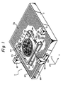
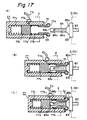
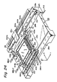
- Fig. 1 is a perspective view showing an overall structure of a stage apparatus 1 in accordance with a first embodiment of the present invention, in which a holder 10 with a semiconductor wafer as a processing substrate plate loaded thereon is provided at its loading surface with an electrode 10a for electrostatic adsorption of the semiconductor wafer thereon.
- the holder 10 is supported by a Z-directional minute motion mechanism and a leveling mechanism (both being referred to herein collectively as a Z/L fine motion mechanism), although not shown in the drawing.
- a movable main stage member 2 is supported so as to be movable two-dimensionally in the Y- and Y-directions along a defined flat plane 3a formed on a base table 3.
- the stage apparatus 1 is of a guideless type having a full flat surface 3a supporting the own weight of the main stage member 2 as a Z-directional guide plane yet having no guide plane for movement in X- and Y-directions.
- the main stage member 2 is provided on its bottom portion with a plurality of electromagnet units (not shown) for generating the magnetic floating force with respect to the flat surface 3a of the base table 3 as well as a plurality of electromagnetic drive units 4a, 4b, 4c and 4d (4d being not shown in this drawing for brevity of illustration), consisting of a plurality of coils, for generating the drive force for transferring the main stage member 2 in directions X, Y and ⁇ are disposed on the bottom side of the main stage member 2.
- the electromagnetic drive units 4a, 4b, 4c and 4d are comprised as a flat motor of a two-dimensional movement type so as to generate the drive force in each direction in association with a number of permanent magnets arranged in a matrix form over substantially the entire surface of the flat surface 3a of the base table 3.
- a stage apparatus having a structure similar to that of the stage apparatus according to the present invention is disclosed, for example, in U.S. Patent No. 4,654,571.
- the prior art stage apparatus may be applied, as needed, to the stage apparatus of Fig. 1 according to a one embodiment of the present invention as it is or with some modifications.
- the stage apparatus 1 of Fig. 1 may also be arranged so as to float the movable main stage member 2 in an air bearing system in a like manner as the prior art stage apparatus by mounting an air pad part on the bottom surface of the movable main stage member 2.
- the main stage member 2 and the holder 10 may be made each of ceramics materials (non-magnetic material having a high insulation) and particularly the inside of the main stage member 2 may be made of a honeycomb structure or a rim structure in order to make the weight of the main stage member 2 lightweight.
- a side edge portion of the main stage member 2 extending in the X-direction is formed integrally with a movable mirror 5Y and a side edge portion thereof extending in the Y-direction is formed integrally with a movable mirror 5X.
- each of the movable mirrors 5X and 5Y has its surface deposited with a reflecting plane extending in the directions X and Y, respectively.
- a laser interferometer 6Y fixed to the base table 3 and an interference beams representative of a variation in the positions of the coordinates relating to the Y-direction of the reflecting plane of the movable mirror 5Y are photoelectrically detected by a receiver 7Y.
- measuring beams for length measurement from a laser interferometer 6X are projected to the movable mirror 5X along the X-direction and interference beams from the reflecting plane of the movable mirror 5X are photoelectrically detected by a receiver 7X.
- beam paths 8X and 8Y are provided at the side edge portion of the base table 3 for supplying laser beams for sending light to the laser interferometers 5X and 5Y, respectively.
- the laser interferometers 6X and 6Y are so configured as to measure the positions of X-directional and Y-directional movements of the main stage member 2 as well as to measure the amount of rotation (yawing in the direction ⁇ ) around the Z-axis of the main stage member 2.
- the drive force of each of the electromagnetic drive units 4a-4d is subjected to servo control on the basis of the measured values in the directions X, Y and a measured by the laser interferometers 6X and 6Y, respectively.
- a portion of the side edge portion of the main stage member 2 is provided with a power receipt terminal part 9a for charging a built-in battery and a power feed terminal part 9b for charging a battery is mounted at the position corresponding to the height of the base table 3 through a base seat 9.
- a base seat 9 In the base seat 9 is mounted an electric power circuit for rapidly charging.
- an optical coupler or an electrical coupler On each of the power receipt terminal parts 9a and the power feed terminal part 9b is mounted an optical coupler or an electrical coupler for implementing various information communications between a microcomputer built in the main stage member 2 and an outside computer for implementing an apparatus-managing control.
- a reference mark plate 14 with a variety of reference marks formed thereon is fixed in the vicinity of an upper surface portion of the main stage member 2 because it is necessary to correct the relationship of the X- and Y-directional positions of the main stage member 2 relative to the position of a pattern projection system, such as an optical projection system for ultraviolet rays (e.g. bright line of a mercury lamp or excimer laser beams) or an electron lens projection system for use in exposure to charged particle rays, etc.
- a pattern projection system such as an optical projection system for ultraviolet rays (e.g. bright line of a mercury lamp or excimer laser beams) or an electron lens projection system for use in exposure to charged particle rays, etc.
- an optical coupler part 12 including a sending light part and a receiving light part on an apparatus column side disposed outside the pattern projection system and a small lens body for implementing optical communications is disposed at another peripheral portion of the main stage member 2.
- a specific structure of the optical coupler 12 and a manner of use thereof are described in detail in Japanese Patent Application No. 8- 229,839 filed by the identical applicant (U.S. Patent Application Serial No. 807159 filed on Feb. 27, 1997) so that a duplicate description will be omitted for brevity of explanation.
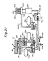
- a rechargeable battery 100 as an energy accumulation member has a plurality of nickel-type batteries with e.g. 7.5 V and 3.600 mAh arranged in an in-line or parallel manner, thereby securing the necessary power capacity.
- a power line from the battery 100 is connected to a aharging/communication coupler circuit 102 to be connected to a power receipt terminal part 9a, a high voltage control circuit 112 to be connected to an electrode 10a for electrostatic absorption of the holder 10, drive circuits 114 and 116 to supply driving electric current to a plurality of electromagnetic coil group XM1, XM2, YM1 and YM2 mounted on the electromagnetic drive units 4a-4d, respectively, and a drive circuit 118 to supply driving signals to each of three motors ZM1, ZM2 and ZM3 by a voice coil type built in the Z/L minute motion mechanism of the holder 10 or by an electromagnetic actuator of an E core type or piezo expansion elements, etc.
- electromagnet units for magnetically float the movable main stage member 2 with relative to the base table 3 and a feed circuit to those units are omitted from Fig. 2, as a matter of course, the electromagnet units for magnetic floating are driven in response to the electrical energy of the battery 100 as needed.
- the stage apparatus 1 of Fig. 2 is provided with the Z/L minute motion mechanisms (ZM1-ZM3), an accuracy in magnetically floating the movable main stage member 2 may not be required to be very high.
- the electromagnet units for magnetic floating can achieve its sufficient performance by an open loop control for supplying a constant electric current from the battery 100 through a simple constant current drive circuit.
- the electromagnet units for magnetic floating are not required at all if the main stage member 2 is floated through a static pressure air bearing.
- a stabilizing power circuit (VRC) 104 is so disposed as to convert a battery voltage from the charging/communication coupler circuit 102 into stabilized power voltage (5V, ⁇ 15 V, etc.) in a DC/DC converter system or the like and supply it to a circuits group having a relatively small consumption of electric power.
- the stabilized power voltage is sent to an RF circuit 106 for receiving or sending electrical wave via an antenna AT in a wireless system, a converter circuit 108 for converting various information to be received or sent via wireless wave between analog signals and digital signals, and a micro-computer (CPU) 110 for controlling an entire electrical circuit system installed in the main stage member 2.
- the antenna AT and the RF circuit or including the converter circuit 108) constitute a transmitter in a wireless system.
- the CPU 110 is connected to a control logic part or a communications interface part in the charging/communication coupler circuit 102 to implement the management and control of the charging state and the management and control of communication ports.
- the interface part installed in the charging/communication coupler circuit 102 may be comprised of an optical communication circuit (e.g. LED, photodiode, modulation-demodulation circuit, etc.), as needed.
- the power feed terminal part 9b on the stage apparatus 1 side of is also provided with a light emitting element or a light receiving element for the optical communication interface.
- the CPU 110 also sends or receives a variety of digital information (e.g. commands, parameters, data, etc.) for communicating with an external host computer in a wireless system to or from the converter circuit 108. Moreover, the CPU 110 can send to the high voltage control circuit 112 information for controlling the adsorption or release of the adsorption of a wafer in response to the commands or parameters sent from the external computer to thereby output the controlling information to each of the drive circuits 114, 116 and 118 at a real time.
- digital information e.g. commands, parameters, data, etc.
- a cycle time of output of instruction values to the drive circuits 114, 116 and 118 require a high speed of the order of mS or higher so that the CPU 110 has preferably a clock frequency of several tens MHz or higher in a microprocessor type.
- the electromagnetic drive units 4a-4d (or electromagnet units for magnetic floating) are connected to the main stage member 2 and the base table 3 via electrical wires in a conventional manner
- the electromagnetic coil groups XM1, XM2, YM1 and YM2 as well as the drive circuits 114 and 116 as shown in Fig. 2 are not required. Therefore, the real time control by the CPU 110 is carried out exclusively by the drive circuit 118 of the Z/L minute motion mechanism, thereby reducing the processing load of the processor consisting of the CPU 110.
- this structure can offer the advantage that a charging cycle of the battery 100 can be extended.
- the high voltage control circuit 112 for the adsorption of a wafer to the holder 10 or for another electrostatic adsorption pad disposed in the main stage member 2 and other small electrical power circuits systems alone are operated by the built-in battery 100. Therefore, the consumption of electrical power by the battery 100 can further be reduced, thereby making the battery more compact in size and lightweight and as a consequence enabling a reduction in the total weight of the main stage member 2.
- the adsorption and the release of the adsorption of the wafer are implemented when the main stage member 2 stops in the loading position and the unloading position, respectively, upon exchanging for wafers. Further, the electrostatic adsorption pad disposed in the main stage member 2 is adsorbed or released generally upon exchanging for wafers. Thus, it is generally acceptable that the power receipt terminal part 9a and the power feed terminal part 9b are connected to each other in the respective positions.
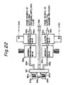
- a projection exposure apparatus of a step-and-scan system to be used in connection with the process for the manufacture of semiconductor memory devices (D-RAM) of 64 Mbit classes or greater, which may be affected by dragging of tubes or wires or for other reasons.
- D-RAM semiconductor memory devices
- the exposure apparatus utilizes pulse laser beams from an excimer laser light source 20 as a light for illumination.
- the excimer laser light source 20 may be of a type emitting KrF excimer laser beams having a wavelength of 248 nm, ArF excimer laser beams having a wavelength of 193 nm and F 2 laser beams having a wavelength of 157 nm as a pulse light, and its wavelength width is narrow-banded so as to allow a color aberration resulting from the material of a variety of optical elements constituting an optical projection system PL of the exposure apparatus to come within a clearance range.
- the absolute value of the central wavelength to be narrow-banded and the value of a narrow-banding width (between 1 pm and 300 pm) are displayed on an operation panel 21 and they can be adjusted as needed from the operation panel 21. Further, the operation panel 21 is so disposed as to set a mode for generating a pulse light (represented by three modes of self-oscillation, external trigger oscillation and oscillation for maintenance).
- the excimer laser light from the excimer laser light source 20 is led to a beams light receiving system 23 of the exposure apparatus through a light-blocking tube 22.
- a plurality of movable reflecting mirrors are so arranged as to adjust the incidence position or the incidence angle of the excimer laser light to an optical illumination system 24 to the optimized position or angle so that the excimer laser light is always incident to the optical axis of the optical illumination system 24 of the exposure apparatus in a predetermined position relationship.
- Some examples of the exposure apparatuses using excimer laser light as a light source in the manner as described hereinabove are disclosed, for example, in Japanese Patent Unexamined Publication Nos. 57-198,631 (U.S. Patent No. 4,458,994), 1-235,289 (U.S. Patent No. 5,307,207), 2.135,723 (U.S. Patent No. 5,191,374), and 2-294013 (U.S. Patent No. 5,383,217).
- Some examples of the exposure apparatuses utilizing the excimer laser light for step-and-scan exposure are disclosed in Japanese Patent Unexamined Publication Nos. 2-229,423 (U.S. Patent No.
- a flyeye lens system for converting excimer laser light into an illumination light having a uniform distribution of intensity
- a reticle blind for restricting reticle illumination light to a rectangular-shaped slit form upon scan exposure
- an image-formation system including a condenser lens
- the illumination light of the rectangular-shaped slit form to be radiated upon the reticle is so arranged as to extend in a longitudinally elongated form in the X-direction (a non-scanning direction) at the center of a circular projection field of the optical projection system PL in Fig. 3, while the Y-directional (scanning directional) width of the illumination light is set so as to be nearly constant.
- the reticle is adsorbed and held on a reticle stage member 26 as shown in Fig. 3 and the reticle stage member 26 is so disposed as to linearly move on a reticle base table 28 with a great stroke in the Y-direction by a linear motor or other means for scan exposure, while to enable a minute movement in the directions X and ⁇ by a voice coil motor (VCM), piezo element or the like.
- the reticle base table 28 is fixed to four columns 29 disposed upright from a main body column table 30 for fixing a flange of the optical projection system PL.
- the main body column table 30 is formed in a box shape with its inside hollow and the base table 3 of the stage apparatus as shown in Fig. 1 is fixed within the hollow inside thereof.
- the structuring elements as shown in Fig. 1 only the movable main stage member 2, the X-directional interferometer 6X and a seat 9 of the power feed terminal part 9b are schematically illustrated in Fig. 3.
- Fig. 3 As shown in Fig.
- the movable main stage member 2 is stayed unmoving in the loading position (a standby position) in which to receive a wafer W supported at a tip end of an arm 42 of a wafer carrier robot 40 or in the unloading position (a standby position) in which to deliver the wafer held on a holder of the movable main stage member 2 to the arm 42. Therefore, the power receipt terminal part 9a and the power feed terminal part 9b are engaged with each other in the state as shown in Fig. 3.
- mount base 32 having a vibration-preventive function for supporting the entire apparatus from the floor.
- the mount bases 32 are supporting the entire weight of the apparatus via air cylinders and are provided each with an actuator for actively correcting the inclination of the apparatus as a whole and the Z-directional displacement thereof as well as the X- and Y-directional displacement of the apparatus as a whole.
- the overall action of the main body of the exposure apparatus as shown in Fig. 3 is managed by a plurality of unit control boards, as referred to collectively as 51, for individually controlling each of the structuring parts in the main body of the apparatus, e.g. the excimer laser light source 20, the optical illumination system 24, the reticle stage member 26, the movable main stage member 2 for a wafer, the carrier robot 40, etc., a minicomputer 52 for controlling each of the control boards 51 comprehensively, and a control rack 50 including the operation panel 53, a display 54, etc.
- a computer on the unit side such as a microprocessor.
- the computers on the unit side executes a series of exposure processes for a plurality of wafers in association with the minicomputer 52.
- the process program is to store information relating to wafers to be exposed (such as the number of sheets to be processed, shot size, shot sequence data, alignment mark location data, alignment conditions, etc.), information relating to reticles to be used (such as kind data of patterns, mark location data of each mark, a size of a circuit pattern area, etc.), and information relating to exposure conditions (such as an amount of exposure, a focus offset amount, an offset amount of a scanning speed, an offset amount of projection magnification, a distortion correction amount, the setting of a value ⁇ of the illumination system, the setting of a value NA of a projection lens system, etc.) as a package of parameter groups.
- information relating to wafers to be exposed such as the number of sheets to be processed, shot size, shot sequence data, alignment mark location data, alignment conditions, etc.
- information relating to reticles to be used such as kind data of patterns, mark location data of each mark, a size of a circuit pattern area, etc.
- information relating to exposure conditions such
- the minicomputer 52 decodes the process programs instructed to be executed and gives the computer on the corresponding unit side an instruction about the action of each of the structuring elements necessary for the exposure processes of the wafers one after another as a command. At this time, whenever the computer on each of the unit sides finishes one command in a normal manner, the status to that effect is sent to the minicomputer 52 and the minicomputer 52 sends a next command to the computer on the unit side in response to the status sent thereto.
- the movable main stage member 2 and the carrier arm 42 are set in the position relationship (standby position) as shown in Fig. 3 in association of the control unit of the movable main stage member 2 with the control unit of the wafer carrier robot 40.
- the program is started in response to a command or a parameter for controlling the charging of a battery or for making communications stored in advance in a microcomputer or the minicomputer 52 in the control unit of the movable main stage member 2.
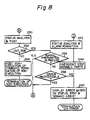
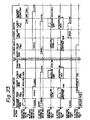
- Fig. 4 shows an example of a flowchart of the program.
- the CPU 110 as shown in Fig. 2 is so disposed as to manage the charging status (data, such as discharging current or discharging time from the full charge time, etc.) of the battery 100 in association with the charging/communication coupler circuit 102.
- the charging status data, such as discharging current or discharging time from the full charge time, etc.
- the power receipt terminal part 9a is connected to the power feed terminal part 9b
- a data coupler part in each of the power receipt terminal part 9a and the power feed terminal part 9b is connected to each other so that the unit computer or the minicomputer 52 for executing the program of Fig. 4 can be made communicatable on software with the CPU 110 on the movable main stage member 2 side.
- the program of Fig. 4 is executable on software in association of the unit computer or the minicomputer 52 with the CPU 110 on the movable main stage member 2 side via transmitter (RFC 106, digital converter 108) in a wireless system as shown in Fig. 2.
- Which communications system is selected, wireless or wire, may be set optionally in accordance with the structure of the exposure apparatus.
- the program of Fig. 4 is executed in association of the minicomputer 52 with the CPU 110 on the movable main stage member 2 side.
- the minicomputer 52 executes a charging management routine of step 55A.
- the minicomputer 52 in this routine reads information relating to the charging status of a battery from the CPU 110 of the main stage member 2 via the RFC 106 in a wireless system is decide to determine if the emergency charging of the battery 100 is needed or not needed on the basis of the information as well as to determine the parameter (e.g. waveform, voltage, frequency, duty, charging time, etc.) for generating the charging voltage to be supplied to the power feed terminal part 9b.
- the parameter e.g. waveform, voltage, frequency, duty, charging time, etc.
- the minicomputer 52 When it is decided that the emergency charging is needed at step 55B, the minicomputer 52 declares the interrupt of the exposure action for the exposure apparatus as a whole at step 55C, thereby temporarily interrupting the action in association with each unit by a plurality of unit computers in the control unit 51 in response to the declaration of the interrupt. It is to be noted herein, however, that the minicomputer 52 sends to a wafer stage control unit a command for transferring the main stage member 2 to the standby position as shown in Fig. 3 at step 55D.
- the computer on the unit side sends to the CPU 110 on the movable main stage member 2 side in a wireless system a variety of subcommands and parameter groups necessary for executing the command.
- This process allows the main stage member 2 to be transferred to the standby position as shown in Fig. 3 to connect the power feed terminal part 9b to the power receipt terminal part 9a and the charging/communication coupler circuit 102 recognized this connection to thereby resume communications with the control unit side in a wire system.
- the CPU 110 sends an instruction in a wireless or in a wire system to a battery charger (disposed in the seat 9 as shown in Figs. 1 and 3) mounted on the base table 3 so as to be controlled by the control unit side, the instruction being to start the charging action in accordance with the various charging parameters decided at step 55A.
- This instruction allows the output electric current for charging to be applied to the battery 100 via the power feed terminal part 9b, the power receipt terminal part 9a and the charging/communication coupler circuit 102 as shown in Fig. 2, thereby effecting the charging in a mode in accordance with the parameters.
- At this time, at least the high voltage control circuit 112 in Fig. 2 may be cut off in order to fail to receive the feed from the battery 100, when the force of adsorption of a wafer on the holder 10 being in the process of exposure can be continued by the residual band charge of the electrode 10a.
- step 55F it is decided to determine if the action of emergency charging has been completed in a normal way.
- the error processing action is terminated on error.
- the action for termination on error may be decided, for example, by the CPU 110 or the computer on the control unit side, and this decision is sent to the minicomputer 52 by a wireless or a wire system thereby causing the minicomputer 52 to issue an alarm giving a notice to the operator that an abnormality has occurred during the charging operation.
- step 55F when the charging operation has been finished in a normal way, the process to resume the exposure action is executed at step 55G.
- This resume process is decided by the CPU 110 or the computer on the control unit side and a notice is sent to the minicomputer 52 by a wireless or a wire system that the exposure action can be resumed. Therefore, upon receipt of this notice, the minicomputer 52 sends a command to each of the control units in the exposure apparatus to resume the action following the status of interrupt of the exposure action.
- the minicomputer 52 decides at step 57A to determine if it is the timing for executing the exchanges for wafers.
- the program of Fig. 4 is allowed to terminate in a normal way. If it is decided that it is the timing for executing the wafers exchanges, on the other hand, the minicomputer 52 executes the processes at steps 57B and 57C.
- the steps 57B and 57C are substantially the same as the processes at steps 55D and 55E, respectively.
- the CPU 110 gives an instruction to the high voltage control circuit 112, upon receipt of the command for the wafers exchanges from the minicomputer 52, that the electrostatic adsorption of the exposed wafer on the holder 10 should be released.
- the release of the adsorption of the wafer can be implemented by quickly discharging the residual band charges accumulated in the wafer and the electrode 10a of the holder 10.
- the high voltage control circuit 112 executes the switching action to release the connection to the electrode 10a and then to earth the electrode 10a or the action to apply reverse bias voltage to the electrode 10a in order to instantly neutralize the band charges.
- the minicomputer 52 gives a command to a wafer carrier control unit that the carrier arm 42 of the wafer carrier robot 40 removes the exposed wafer from the holder 10 and that it carries an non-exposed wafer to the holder 10 and places it thereonto. This allows the exposed wafer to be unloaded from the holder 10 and the non-exposed wafer to be loaded onto the holder 10.
- step 57F an instruction to electrostatically adsorb the non-exposed wafer onto the holder 10 is given to the high voltage control circuit 112.
- step 57G the CPU 110 sends the information to the minicomputer 52 via a wireless system or a wire system that a series of the actions for the wafers exchanges has been completed.
- the apparatus can be made lightweight as only the battery 100, the charging/communication coupler circuit 102 and the high voltage control circuit 112 are required to be loaded on the movable main stage member 2, in instances where the electrical drive systems (e.g. XM1-XM3, ZM1-ZM3, etc. in Fig. 2) to be loaded on the movable main stage member 2 are not driven by the battery 100 and are driven exclusively by an electrostatic chuck alone.
- the electrical drive systems e.g. XM1-XM3, ZM1-ZM3, etc. in Fig. 2
- an electrolytic capacitor having a large capacity may be employed as the battery 100 in accordance with an average period of time during which one sheet of a substrate plate to be exposed or to be processed is kept being adsorbed on the holder 10 for an exposure operation or a processing operation.
- a battery or a condenser is mounted as a self-sustaining power source on the movable main stage member, thereby enabling an amplification and processing of a variety of detection signals from a temperature sensor for monitoring a variation in the temperature of each part of the movable main stage member, an optical sensor for optoelectrically detecting on the movable main stage member the intensity of light (e.g. illumination light for exposure or rays of light from the image of a pattern on a reticle) to be irradiated through the optical projection system PL, an acceleration sensor to be mounted on the movable main stage member for controlling a vibration-proofing actuator disposed to the mount part 32 as shown in Fig. 3 or a gas sensor for monitoring the concentration of oxygen or ozone around the exposing substrate plate, the state of inert gases, etc., mounted on the main stage member 2.
- a temperature sensor for monitoring a variation in the temperature of each part of the movable main stage member
- an optical sensor for optoelectrically detecting on the
- stage apparatus as shown in Figs. 1 and 2 is so adapted as to achieve the object particularly without the use of a flexible tube for use otherwise in vacuum adsorption of a substrate plate to be exposed by effecting the adsorption of the substrate plate in an electrostatic system. Therefore, the stage apparatus as shown in Fig.
- 1 and 2 can also achieve the effects by utilizing an exposure apparatus for effecting exposure in vacuum atmosphere with rays of charged particles (electron beams) or an apparatus for exposing the substrate plate in atmosphere of inert gases (nitrogen or helium gases) with ultraviolet rays having a wavelength of 200 nm or shorter or with soft X-rays (with a wavelength range from approximately 1 ⁇ to 300 ⁇ )(SOR exposure art) or the like, in addition to an apparatus for exposing the substrate plate in open air as shown in Fig. 3.
- an exposure apparatus for effecting exposure in vacuum atmosphere with rays of charged particles (electron beams) or an apparatus for exposing the substrate plate in atmosphere of inert gases (nitrogen or helium gases) with ultraviolet rays having a wavelength of 200 nm or shorter or with soft X-rays (with a wavelength range from approximately 1 ⁇ to 300 ⁇ )(SOR exposure art) or the like in addition to an apparatus for exposing the substrate plate in open air as shown in Fig. 3.
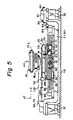
- the stage apparatus of Fig. 5 is structured with the presumption that it is loaded on the projection exposure apparatus as shown in Fig. 3.
- the structuring parts functioning in the same manner as the structure of the apparatus as shown in Figs. 1 and 3 are provided with the identical reference numbers and symbols.
- the stage apparatus as shown in Fig. 5 is not of such a guideless structure as illustrated by the apparatus as shown in Fig. 1 and in an air bearing guide system, which comprises three linearly drivable motors (linear motors) disposed in a H-letter shape, a linearly fixed guide member fixed to a table of the apparatus, a movable guide member disposed as to be movable along the fixed guide member and extending in a direction intersecting at a right angle with the fixed guide member, and a movable main stage member disposed so as to move the table of the apparatus by guidance with the movable guide member, in which each of the guide surfaces is supported in a non-contact fashion by a static pressure gas bearing.
- linearly drivable motors linear motors
- a linearly fixed guide member fixed to a table of the apparatus
- a movable guide member disposed as to be movable along the fixed guide member and extending in a direction intersecting at a right angle with the fixed guide member
- stage apparatuses having such a structure are disclosed, for example, in Japanese Patent Unexamined Publication Nos. 59-101,835 (U.S. Patent No. 4,655,594), 61-209,831 and 1-188,241 (U.S. Patent No. 5,040,431), and the technology disclosed therein may be applied to the stage apparatus according to the second embodiment of the present invention as it is or, as needed, with some modifications.
- the stage apparatus as shown in Fig. 5 is characterized particularly by the features that no tube is used at all or the number of tubes can be reduced, the tube or tubes being connected from a fixed part of the apparatus to a closed space part (a reduced pressure path or an elevated pressure path) in which the reduced pressure state or the elevated pressure state can be maintained at a predetermined level, such as a vacuum adsorption part or an air cylinder, loaded in the movable part of the stage apparatus.
- the main body of the exposure apparatus (the main stage member 2) is held through four mount bases 32 on a floor FD of a plant for producing semiconductor circuit elements.
- an apparatus column 30 acting as the base table 3.
- On the base table 3 is held a lower stage portion 2b through a plurality of static pressure gas pads 62 acting as an air bearing so as to be movable in a two-dimensional direction, the lower stage portion 2b constituting a portion of the movable main stage member 2 and having a movable guide member 60 disposed at its inner central portion so as to move in the X-direction, i.e. the leftward-and-rightward direction on the paper surface of Fig. 5.
- the movable guide member 60 has a guide surface extending in the direction (Y-direction), i.e. in the direction perpendicular to the paper surface of Fig. 5 and is held on the base table 3 through an electrostatic pressure fluid pad 61.
- the guide surface of the movable guide member 60 is structured such that it is held in the Y-direction between the plural static pressure gas pads disposed inside the lower stage portion 2b.
- the movable guide member 60 has a magnets track disposed in the X-direction, which is magnetically connected to a coil unit 63 fixed to the lower stage portion 2b.
- a linear motor is formed between the lower stage portion 2b and the movable guide member 60 so as to move the lower stage portion 2b in the Y-direction along the guide surface of the movable guide member 60.
- the movable guide member 60 is restrained via air bearing on an X-directionally extending guide surface of a fixed guide member 65 fixed on the base table 3. Further, the movable guide member 60 is provided with driving force in the X-direction by a linear motor 66 mounted on the base table 3 in the position parallel to the fixed guide member 65, thereby moving the lower stage portion 2b in the X-direction integrally with the movable guide member 60 when the linear motor 66 is driven.
- an upper stage portion 2a On the upper side of the lower stage portion 2b is mounted an upper stage portion 2a through the Z/L minute motion mechanism including three motors ZM1, ZM2 and ZM3 (only ZM1 being illustrated in Fig. 5 as a representative example), and the upper stage portion 2a has the holder 10 mounted thereon, which in turn is so arranged as to adsorb a wafer W in a vacuum way.
- the loading surface of the holder 10 on which the wafer W is loaded is formed with a plurality of fine projections (e.g. 1 mm in height) each in a ring shape, in a dot shape or a linear shape.
- the Z/L minute motion mechanisms as disclosed in those prior art patent publications may be driven by plural small-size rotary motor, piezo expansion elements or the like and they may also be driven by a voice coil type motor or a direct-acting motor utilizing repelling force or sucking force of an electromagnetic power, such as an E core electromagnet, as driving force for a direct minute motion.
- an electromagnetic power such as an E core electromagnet
- the movable mirror 5X On a peripheral portion of the upper stage portion 2a is fixed the movable mirror 5X having substantially the same structure as that as shown in Fig. 1, which in turn is disposed to allow a measurement of the X-directional position of the coordinates of the upper stage portion 2a by the laser interferometer 6X and the receiver 7X.
- the movable mirror 5Y is also disposed in substantially the same manner to measure the Y-directional position of the coordinates thereof.
- the laser interferometer 6X is disposed so as to project laser beams LBm for length measurement onto two Z-directionally different locations of the reflecting plane of the movable mirror 5X
- the receiver 7X is disposed so as to measure an amount of a lateral deviation of the wafer W due to the driving of the Z/L minute motion mechanism by measuring an amount of a variation in inclination (pitching) of the reflecting plane of the movable mirror 5X with respect to the X-Z flat plane.
- the laser interferometers system 6X and 7X (6Y and 7Y) can measure the X-directional and Y-directional positions of the coordinates of the upper stage portion 2a, yawing (a minute rotation in the direction ⁇ ), and the pitching (a minute inclination with respect to the X-Y flat plane).
- the laser interferometers system allows the length measurement on the basis of interference of the reflecting laser beams of reference laser beams LBr with the reflecting laser beams of the length-measuring laser beams LBm, the reference laser beams LBr being projected onto a fixed mirror MLx mounted on the bottom portion of a mirror cylinder of the optical projection system PL and the length-measuring laser beams LBm being reflected from the movable mirror 5X.
- the mirror cylinder of the optical projection system PL is fixed to an apparatus column by a flange part FLg so as to allow its optical axis AX to become perpendicular to the X-Y flat plane (a defined flat plane of the base table 3).
- a pressure-reducing fluid for causing the wafer W to be vacuum adsorbed on the holder 10 may be supplied from a receipt edge orifice 70 fixed to a peripheral edge of the upper stage portion 2a.
- the receipt edge orifice 70 is so disposed as to come into abutment with a feed edge orifice 84 fixed on the base table 3 side or the apparatus column 30 side, when the movable main stage member 2 (2a and 2b) is moved to the loading position for wafers exchanges.
- the pressure-reducing fluid fed through the receipt edge orifice 70 is supplied to the upper stage portion 2a via an electromagnetic valve unit 71 and a tube 73 and then to the loading surface of the holder 10 via the inside of the upper stage portion 2a.
- the electromagnetic valve unit 71 is to switch between the opening of the receipt edge orifice 70 to the atmosphere and the closing of a passage of the fluid, in response to the electrical signals.
- a reserve tank 72 communicating with the tube 73 during the action of adsorption of the wafer W.
- the reserve tank 72 is disposed in order to solve the disadvantages that a total pressure-reduced volume extending from the pressure-reducing layer formed on the loading plane of the holder 10 to the tube 73 is so extremely small that the action of adsorption of the wafer W cannot be sustained by the volume alone over a period of time long enough to complete the exposure action of the wafer W.
- the such disadvantages may be caused to occur mainly due to the fact that the pressure-reducing fluid may be leaked to an extremely slight extent on account of irregularity in the order of microns on the rear surface of the wafer which comes into tight contact with the loading surface of the holder 10.
- a flow amount of a leakage of the pressure-reducing fluid may vary greatly with the extent of unevenness on the rear surface of the wafer and, generally, heat processed wafers may have the tendency that a flow amount of the leaked fluid becomes greater.
- the exposure apparatus of this sort implements the exposure in such a state that the wafer W is aligned with a projection image of a reticle with accuracy of approximately one of fifth or smaller (e.g. ⁇ 0.04 micron) of the width of an image resolving line. This alignment accuracy should be maintained over the entire period of time during which one sheet of a wafer is being subjected to processing for exposure.
- the wafer adsorbed on the holder 10 has its adsorption force defined so as to fail to minutely move to such an extent that the alignment accuracy causes deteriorating over a period of time ranging from the start of the alignment action of the wafer W (the action to detect the position of a wafer mark of the wafer W) to the completion of exposure of plural shot areas on the wafer W.
- the adsorption force may vary with a planar disposition of the plural projections formed on the loading surface of the holder 10, a rate of the contact area of the projections with respect to the rear surface of the wafer therewith, etc., it depends dominantly upon a variation in vacuum pressure.
- the adsorption force for adsorbing the wafer W on the holder 10 can be sustained at a predetermined level over a long period of time (during the time when the wafer is loaded on the holder 10 at least for exposure processing), even if an extremely slight amount of the pressure-reducing fluid would be leaked, by disposing the reserve tank 72 through the path through which to flow the pressure-reducing fluid, as shown in Fig. 5.
- the reserve tank 72 may be built in the lower stage portion 2b, although it may be attached outside a portion of the lower stage portion 2b as shown in Fig. 5. Further, the electromagnetic valve unit 71 may be provided with a pressure sensor (a vacuum sensor) for detecting the pressure within the reserve tank 72 or the tube 73, thereby sending the detected information to a board for stage control in the control unit 51 installed in the control rack 50.
- a pressure sensor a vacuum sensor
- the electromagnetic valve unit 71 is provided therein with a variable restricting valve (a speed controller) for adjusting a flow amount of the pressure-reducing fluid to be fed to the loading surface of the holder 10 through the tube 73.
- the variable restricting valve is so arranged as to restrict the flow amount of the pressure-reducing fluid passing through a path for supplying vacuum pressure at the time of starting the adsorption of the wafer in order to ensure a stable and sure adsorption of the wafer W on the holder 10 without a deviation of the position of the wafer W.
- the feed edge orifice 84 engageable with the receipt edge orifice 70 may be mounted on a portion of the apparatus column 30 or the base table 3 by the aid of a fixing member 83 and be connected to a fluid supply system 81 through a tube 82.
- a tube 80 extending from a source for vacuum original pressure or compressed dry air disposed in a plant.
- an electromagnetic valve for sending the pressure-reducing fluid (vacuum pressure) to the feed edge orifice 84 through the tube 82 or blocking the passage of the pressure-reducing fluid thereto.
- Fig. 6 is a schematic block diagram showing a piping line of the apparatus, in which the same structuring parts as those in Fig. 5 are provided with the identical reference numerals and symbols.
- the holder 10 is provided on its surface with a plurality of fine projection parts 90 as shown in Fig. 6.
- the fine projection parts 90 are comprised of plural projections each of a ring shape, with narrower space portions (concave portions) 91 and wider space portions (concave portions) 92 arranged alternately in the radial direction, as illustrated in Japanese Patent Unexamined Publication No. 1-319,965.
- a small ring-shaped groove defined by the narrower space portion 91 is structured as a pressure-reducing part for vacuum adsorption and a ring-shaped concave portion defined by the wider space portion 92 is comprised as an area in which the pressure is allowed to be released into open air and the pressure therein becomes slightly negative during the time of adsorption.
- the holder 10 is mounted on the upper stage portion 2a.
- Each of the ring-shaped grooves 91 for adsorption on the holder 10 is communicated with a pressure-reducing path 93 formed in the holder 10, which in turn is connected to a tube 73, as shown in Fig. 5, through a 0-ring OS, made of rubber or plastics material.
- the pressure within each of the ring-shaped grooves 91 on the holder 10 is reduced by supplying the pressure-reducing fluid (vacuum pressure) thereto through the tube 73, thereby allowing the wafer W to be adsorbed and fixed in a tight contact state on each of the top surface portions of the ring-shaped projection parts 90 of the holder 10.
- the wafer W may be flattened in accordance with a plane accuracy (for example, less than plus or minus approximately 1 micron) defined by the surface of each of the fine projection parts 90.
- the tube 73 is connected to the electromagnetic valve unit 71 fixed to the lower stage portion 2b.
- the electromagnetic valve unit 71 includes a pipe 70a leading the pressure-reducing fluid from the receipt edge orifice 70 thereto, an electromagnetic valve 71a for switching the opening of the pipe 70a to open air or the blocking therefrom, a valve drive part 71b of the electromagnetic valve 71a, a variable restricting valve 71c for adjusting a flow speed rate of the pressure-reducing fluid from the electromagnetic valve 71a, an adjustment thumbscrew 71d of the variable restricting valve 71c, and a pressure sensor 71e for monitoring the adsorption force of the wafer by detecting the negative pressure of the pressure-reducing path extending between the ring-shaped grooves 91 of the holder 10 and the tube 73. Further, the pressure-reducing path extending between the electro-magnetic valve 71a and the variable restricting valve 71c is connected to a pipe 71f communicating with the reserve tank 72.
- Fig. 6 shows the status in which the movable main stage member 2 (2a and 2b) is stayed at its standby position and the receipt edge orifice 70 is engaged with the feed edge orifice 84 held on the side of the base table 3 or the apparatus column 30 through the fixing member 83.
- the feed edge orifice 84 is made of elastic material and in a ring shape having a circular opening portion that can tightly engage with the metal pipe and communicates with the receipt edge orifice 70.
- the circular opening portion of the feed edge orifice 84 may be formed in such a conical shape that the diameter of its outer side is greater and that of its inner side becomes gradually smaller.
- the metal pipe of the receipt edge orifice 70 can be inserted readily and surely into the circular opening portion of the feed edge orifice 84 simply by minutely moving the movable main stage member 2 in the Y-direction with a predetermined driving force.
- each of the metal pipe of the receipt edge orifice 70 and the opening portion of the feed edge orifice 84 with a highly viscous oil (grease) forming a thin coating, in order to prevent a leakage during connection.
- a highly viscous oil greye
- a bellows 85 with a relatively high degree of elasticity, and the feed edge orifice 84 is so disposed as to be oscillatable in a slight range to absorb a deviation in the position of the receipt edge orifice 70 relative to the position of the feed edge orifice 84, which may be caused to occur upon connection of the metal pipe of the receipt edge orifice 70 with the feed edge orifice 84.
- the fluid supply system 81 fixed on the side of the base table 3 or the apparatus column 30 is disposed therein with an electromagnetic valve 81a and a drive part 81b for driving the valve, the electromagnetic valve 81a being so arranged as to switch between passing of the pressure-reducing fluid (vacuum pressure) for sending to the feed edge orifice 84 through the tube 82 and blocking the passage of the pressure-reducing fluid and being connected through the tube 80 to a source of vacuum original pressure disposed in the plant.
- the pressure-reducing fluid vacuum pressure
- signals SV1 and SV2 are sent each to the drive part 81b of the electromagnetic valve 81a and the drive part 71b of the electromagnetic valve 71a from a control board 51a for controlling a wafer carrier unit among control units 51 in the control rack 50 as shown in Fig. 3.
- the electromagnetic valves 71a and 81b are so arranged as to open the pressure-reducing path and close it in response to the signals SV1 and SV2, respectively.
- the pressure sensor 71e sends a signal Sp to the control board 51a in accordance with the pressure (negative pressure) detected thereby, and a computer installed in the control board 51a generates information about a predetermined alarm in accordance with the program for monitoring the status of adsorption of the wafer on the basis of the signal Sp.
- the alarm information is employed primarily for the object to rapidly cease the action of the exposure apparatus in case of emergency for ensuring safety in instances where the adsorption of a wafer cannot be implemented at all.
- the alarm information is employed for the object to decide if the program should be executed to implement the action to adsorb the wafer again immediately before the event occurs that the adsorption of the wafer cannot be implemented in a proper way or to execute the action to cease the exposure of the wafer on error, by monitoring a periodical variation in the adsorption of the wafer.
- Such a program for monitoring the adsorption of the wafer to generate such an alarm information will be described in detail later.
- the computer in the control board 51a is connected to an upper minicomputer 52 and a lower carrier robot 40 through a parallel bus or a serial bus such as GP-IB, optical fibers, RS232C or the like.
- the minicomputer 52 sends a global command to the control board 51a through the such bus in a status according to the communications regulations of SECS, the global commands including "CARRY WAFER”, “EXCHANGE WAFERS”, “WAITING", "INITIALIZE” and the like.
- the computer in the control board 51a executes plural sets of programs in response to the such global command, the plural sets of the programs consisting of plural subcommands and parameters for controlling the specific actions of each part of the carrier mechanism such as the wafer carrier robot 40 and the like.
- the flowchart of each of Figs. 7-9 and 11 mainly indicates the primary actions to carry wafers and to exchange for wafers in accordance with the program stored in the computer of the control board 51a of the wafer carrier control unit.
- a description will be made with the presumption that one sheet of a wafer W is loaded (vacuum adsorbed) on the carrier arm 42 as shown in Fig. 3 in such a state that it is pre-aligned mechanically.
- the program A as shown in Fig. 7 indicates the primary actions ranging from the action to execute the global command of "EXCHANGE WAFERS" upon sending it thereto from the minicomputer 52 to the action to adsorb a new wafer (a non-processed wafer) on the holder 10 when no processed wafer is located on the holder 10.
- step 200 it is decided to determine whether the wafer carrier control unit is in a wafer-exchangeable state in which to exchange wafers from the physical and timing point of view.
- the "wafer-exchangeable state" referred to herein is intended to mean the state that should satisfy two points, one being such that a new wafer for exchange (for loading) is pre-aligned in a normal way and is already in a state ready for exchange and the second being such that the movable main stage member 2 is not shared with another wafer for the exposure action. Therefore, when it is decided at step 200 that the wafers exchanges cannot be conducted, the action for the wafers exchanges is not implemented, followed by proceeding to a process routine for a system error in accordance with a program B (Fig. 8). On the other hand, when the decision is made at step 200 to implement the wafers exchanges, then the program goes to step 202.
- step 202 the signal Sp from the pressure sensor 71e disposed in the electromagnetic valve unit 71 as shown in Fig. 6 is read, followed by deciding to determine if the read value is a value in accordance with atmospheric pressure or not. This decision is executed to investigate whether a wafer is adsorbed on the holder 10 of the movable main stage member 2 or not.
- step 202 the actions following the program A are not implemented, followed by executing a wafers exchanges routine in accordance with a program C (Fig. 9).
- step 204 is executed.
- an arm transfer instruction (A1) is sent to move the carrier arm 42 of the wafer carrier robot 40 to the loading position for loading a non-processed wafer located on the carrier arm 42 of the wafer carrier robot 40.
- This instruction allows the non-processed wafer to be transferred to the loading position on the X-Y flat plane while maintaining the Z-position higher than the surface of the holder 10.
- a stage transfer instruction (S1) is sent in order to transfer the movable main stage member 2 toward the loading position, in substantially the same manner as at step 204.
- the movable main stage member 2 is allowed to transfer the metal pipe of the receipt edge orifice 70, as shown in Figs. 5 and 6, to the position facing the right front face of the feed edge orifice 84 at an interval apart by several millimeters and to stop the movement of the mental pipe of the receipt edge orifice 70 in the stop position.
- the stop position referred to herein is the unloading position in which to remove the exposed wafer, in this embodiment, from the holder 10.
- step 208 there is confirmed the original pressure of the vacuum source to be fed to a pipe 80 as shown in Fig. 6, while executing step 206 in parallel thereto.
- the original pressure is confirmed by reading the detected value of a pressure gauge not shown in Fig. 6.
- this confirmation is not absolutely required, it is preferred to effect this confirmation in order to avoid in advance inconveniences to be caused to occur due to the fact that a wafer is loaded on the holder 10 at an abnormal original pressure. That the original pressure of the vacuum source is outside a pre-determined pressure range means an occurrence of serious inconveniences in the operating environment itself of the apparatus, in addition to the action of adsorption of a water, or a future occurrence of such abnormality.
- a program D (Fig. 8) is executed to give a notice of abnormality in the operating environment of the apparatus.
- the movable main stage member 2 is stopped in the position in which the receipt edge orifice 70 is slightly apart from the feed edge orifice 84 in the vicinity of the loading position (an unloading position in this embodiment), thereby bringing the movable main stage member 2 into the waiting state for assistance by the operator.
- the control board 51a sends to the drive part 71b the signal SV2 to open the electromagnetic valve 71a.
- the electromagnetic valve 71a is switched into an open state as shown in Fig. 6.
- a minute motion instruction (S2) for a minute motion is sent to accurately align the movable main stage member 2 with the loading position at the same time as step 212 is sent.
- the movable main stage member 2 is minutely moved so as to allow the metal pipe of the receipt edge orifice 70 to move in a straight way toward the opening part of the feed edge orifice 84 and to engage the metal pipe of the receipt edge orifice 70 with the opening part of the feed edge orifice 84 with each other.
- the linear motors 63 and 66 as shown in Fig. 5 are subjected to servo control on the basis of the position information about the positions of the laser interferometers 6X and 6Y, respectively, so as to stop the movable main stage member 2 at the position.
- a delivery instruction (A2) to deliver a non-processed wafer to the holder 10 is given by lowering the carrier arm 42 of the wafer carrier robot 40 at the same time as at step 212.
- This instruction allows the non-processed wafer to be loaded on the loading surface of the holder 10 as shown in Fig. 6, and the carrier arm 42 to be evacuated from a space on the holder 10.
- the signal SV1 to open the electromagnetic valve 81a is sent to the drive part 81b concurrently with step 214.
- the electromagnetic valve 81a is opened during this period of time, thereby supplying the vacuum pressure to the pressure-reducing path extending between the source of the original vacuum pressure and the adsorption groove 91 of the holder 10 and to the reserve tank 72.
- the pressure inside the reserve tank 72 is reduced up to substantially the same level as the source of the vacuum original pressure.
- variable restricting valve 71c is disposed in the vacuum path extending to the adsorption grooves 91 of the holder 10, some delay (approximately within 1 second) is caused to happen until the pressure within the adsorption grooves 91 is reduced to the level substantially identical to the source of the vacuum original pressure, even if the rear surface of the wafer is allowed to come into tight contact with the fine projection parts 90 of the holder 10 to form the flow path between the receipt edge orifice 70 and the adsorption grooves 91 into a closed space.
- step 218 the action to wait for a timer is executed while a delay in time may be expected to occur.
- step 218 is not absolutely necessary.
- the signal Sp is read from the pressure sensor 71e and it is then decided to determine if the read value is present in the range of pressure to be present at the time of vacuum adsorption.
- the pressure of the source of the original vacuum pressure is set at approximately 350 mmHg
- it is decided that the adsorption force is ensured to a predetermined level when the detected pressure is present, for example, within ten several percentage, i.e. in the range of 350 mmHg to 390 mmHg, followed by proceeding to step 222.
- the program E for re-trying the carrying of the wafer is basically to carry out an operation for unloading a non-adsorbed wafer on the holder 10 in a pre-alignment mechanism and re-executing the actions following the pre-alignment action.
- a detailed description thereof is omitted here.
- the signals SV1 and SV2 for closing the two electromagnetic valves 71a and 81a are sent to the drive parts 71b and 81b, respectively, thereby switching the vacuum adsorption path on the movable main stage member 2 side to the state in which to cut off the path from open air and sustaining the wafer in an independently self-sustaining adsorption state by the vacuum pressure within the reserve tank 72.
- a gap of I micron or smaller may be caused to occur partially between the rear surface of the wafer and the contact surface of the fine projection parts 90 of the holder 10 due to microscopic roughness on their surfaces. Therefore, the pressure-reducing fluid is leaked gradually to reduce the vacuum pressure so that, in this embodiment, a program (Fig. 12) for monitoring the ability of sustaining the adsorption force of the wafer by the reserve tank 72 is set so as to be startable.
- the decision is made to determine whether the program for monitoring the adsorption is turned on or not. when it is decided herein that the program is not turned on, on the one hand, a series of the actions for the wafers exchanges and the wafer adsorption in accordance with the program A has been finished, followed by proceeding to the next step 226, when the monitoring of adsorption is to be implemented.
- the decision at step 224 is made to check if the setting for monitoring the adsorption of the wafer is actually made. This program for monitoring the wafer adsorption is set to be automatically started in usual cases, unless the setting is otherwise released under special situations, such as due to a maintenance of the apparatus.
- step 224 when it is decided at step 224 that the program for monitoring the wafer adsorption is not ready for start, this situation is noticed to the minicomputer 52 through a bus line and an alarm or a display to that effect is given to the operator. It is to be noted herein that when the exposure apparatus is set to a usual large-scale production mode, the program for monitoring the wafer adsorption may be set to be started without conditions.
- step 226 upon starting the program for monitoring the wafer adsorption, the signal Sp from the pressure sensor 71e immediately after the start of the self-sustaining adsorption is read and stored and a timer for monitoring the leak time of the vacuum pressure (the time for maintaining the adsorption force) and the like is started.
- the program for monitoring the wafer adsorption (Fig. 12) is started at the time of starting the self-sustaining adsorption of the wafer by the reserve tank 72 and continued until the wafer is detached from the holder 10.
- the monitoring program ie set so as to read the value of the signal Sp and the count time of the timer at every constant time or whenever a certain command relating to the driving of the movable main stage member 2, thereby computing the prediction of a variation in the adsorption force of the holder 10 and preparing a variety of alarm information on the basis of the result of computation.
- step 226 The actions for carrying the wafers and adsorbing the wafer in accordance with the program A are completed by step 226.
- the notice of this completion is given to the minicomputer 52 as one global command having been finished in a normal manner.
- the movable main stage member 2 moves in a two-dimensional direction under the optical projection system PL as shown in Fig. 3 in response to various global commands to be given by the minicomputer 52 in order to execute an alignment action for detecting the mark on the wafer, an exposure action for transcribing a circuit pattern onto each shot area on the wafer, and the like.
- step 230 of the program B the action status of each part in the wafer carrier control unit is read and analyzed in order to learn the cause of disablement of exchanging wafers at the time of receipt of a global command from the minicomputer 52. The result of analysis is reported to the minicomputer 52. Then, at step 232, it is decided from the result of analysis to determine whether the disablement of the wafers exchanges is caused to occur by failure on the part of the wafer carrier control unit (robot 40) or on the part of the movable main stage member 2.
- step 232 when it is decided at step 232 that the disablement of exchanging the wafers is caused due to the problems on the part of the wafer carrier unit, the decision is further made at step 236 on the basis of the analyzed status information to determine whether the disablement is caused by a simple delay in carrying the wafer through the wafer carrier control unit (in the process of a normal preparation) or by an error.
- the action is simply to wait for the wafer being carried to a predetermined position and, once the wafer has been carried to the given position, then the actions followed by the first step 200 of the program A are re-executed.
- step 236 When the decision is made at step 236 that the disablement of the wafers exchanges is caused by an error in the wafer carrier control unit, it is further decided at step 238 to determine if the error is recoverable. When the error is found recoverable, then the actions followed by the first step 200 of the program A are re-executed in order to wait for an automatic return action in the wafer carrier control unit. When the error is non-recoverable at step 238 to the contrary, then the action proceeds to step 240 at which a notice of the contents of the error in accordance with the result of analysis of the status is given to the minicomputer 52.
- step 242 of the program D the status of the actions in the wafer carrier control unit is analyzed and an alarm information in accordance with the status is prepared, by taking into account the instance where the disablement of the vacuum adsorption of the wafer is caused by abnormality in the source of the original vacuum pressure.
- step 244 each of the movable parts of the wafer carrier control unit is emergency stopped in order to ensure security of the wafer and the apparatus.
- step 240 is executed in the manner as described hereinabove, followed by giving a notice to the minicomputer 52 of the error contents in accordance with the analyzed status.
- an occurrence of an error is displayed on the display screen 54 as shown in Fig. 3 and sending an assist demand (an alarm) to the operator.
- a notice of the termination on error to the global command for exchanging the wafers is given to the minicomputer 52 and the program B (and the program A) is terminated on error.
- the action for exchanging wafers by the program C includes the work to exchange the exposed wafer loaded on the holder 10 of the movable main stage member 2 for a non-processed wafer held on the carrier arm 42 of the wafer carrier robot 40.
- the wafer carrier robot 40 is provided with a weight arm 42 for temporarily holding a wafer at the time of exchanging the wafers, in addition to the carrier arm 42.
- the weight arm 41 and the carrier arm 42 are structured in a manner as described in Fig. 10. Therefore, a brief description will be made of the structure and the actions of the wafer carrier robot 40 with reference to Fig. 10 before a description is made of the action for exchanging the wafers as shown in Fig. 9.
- Fig. 10 shows the wafer carrier robot 40 when looked on the X-Y flat plane.
- the carrier arm 42 comprises an arm of an articulate type consisting of three arm joints 42a, 42b and 42c.
- the arm joint 42a disposed at the top of the arm so as to adsorb a wafer is structured such that it moves linearly in the Y-direction by rotating the arm joint 42c with a drive part 40a.
- the drive part 40a is in turn structured so as to move upward and downward in the Z-direction (in the direction perpendicular to the surface of this paper) with respect to the main body of the wafer carrier robot 40, thereby enabling a Z-directional movement of the wafer adsorbed on the arm joint 42a.
- the main body of the wafer carrier robot 40 is provided with the weight arm 41 that is movable upward and downward in the Z-direction.
- the weight arm 41 is disposed at a portion of a Y-directionally extending path for carrying a wafer by the arm joint 42a, thereby allowing the wafer in the process of carrying to be temporarily held by vacuum adsorption.
- the weight arm 41 is so arranged as to move upward and downward in a distance extending between the Z-position higher than the position of the arm joint 42a for carrying the wafer and the Z-position lower than the position thereof.
- the reason why the loading position LDP is deviated from the unloading position ULP in the Y-direction is because, as is apparent from the structure as Shown in Fig. 6, the pressure-reducing path extending between the adsorption grooves 91 of the holder 10 and the receipt edge orifice 70 is exposed to open air upon lifting the wafer W from the holder is at the time of unloading the wafer W therefrom.
- the empty weight arm 41 is evacuated to the Z-position so as to fail to interfere with the locus of the transferal of the wafer W' or W" by the Y-directional movement of the arm joint 42a, in this embodiment, to the Z-position lower than the position of the arm joint 42a.
- the weight arm 41 stops in the Z-position that substantially coincides its Y-directional center 41c with the center of the wafer W' or W" in the process of being carried, it receives the wafer from the arm joint 42a by moving upward or downward, Then, the weight arm 41 is evacuated to the Z-position higher than the position of the arm joint 42a.
- a pre-alignment mechanism 43 is disposed ahead of the wafer carrier robot 40 having the structure as shown in Fig. 10 for aligning a non-processed wafer W' so as to arrange an orientation flat or a notch thereof in one direction.
- the non-processed wafer W' is loaded first on a rotary table 43a of the pre-alignment mechanism 43.
- the arm joint 42a delivers the exposed wafer W" on the holder is to the weight arm 41 and then the arm joint 42a holds a non-exposed wafer W" on the rotary table 43a and carries it to the loading position LDP. Thereafter, the arm joint 42a carries the exposed wafer W" on the weight arm 41 to a predetermined wafer store position (e.g. a wafer cassette, a carrier transfer position of in-line, etc.) and delivers it thereto. Then, the arm joint 42a receives a non-exposed wafer W' from the wafer store position, followed by carrying it to the rotary table 43a.
- a predetermined wafer store position e.g. a wafer cassette, a carrier transfer position of in-line, etc.
- the status information prepared by the control board 51a of the wafer carrier control unit is read and analyzed.
- the status information includes information on a variation in the position of a wafer being in the process of being carried, the status of the action of each of the drive parts, etc., information representative of the presence or absence of an error at real time and may comprise bit patterns of 32-255 bits or a data table of multiple bytes. Therefore, the CPU in the control board 51a reads the contents of the bit patterns or the data table and analyzes the status of carrying the wafers at this point of time to check whether or not there is a problem with the action of carrying the wafers.
- step 252 as a result of the analysis of the status, it is decided to determine if the movable main stage member 2 shares its action with the action executed in response to the previous global command for executing the exposure process or the like.
- the wafer carrier control unit waits for the termination of the action of the main stage member 2, while returning to step 200 et seq. of the program A as shown in Fig. 7. Once the action of the main stage member 2 has been completed, then the following step 254 is executed.
- step 254 there is given an instruction (53) for transferring the main stage member 2 so as to cause the center of the exposed wafer on the holder is to be aligned with the unloading position ULP as shown in Fig. 10.
- the unloading position ULP is located in the position in which the pipe of the receipt edge orifice 70 as shown in Fig. 6 is apart by several millimeters from the front face of the opening portion of the feed edge orifice 84.
- the next step 256 is executed before the main stage member 2 stops in the unloading position ULP, thereby reading and analyzing the status information in the same manner as at step 250.
- step 258 it is decided to determine if a wafer is adsorbed on the carrier arm 42 (42a in Fig. 10) on the basis of the analyzed status information.
- the wafer is a non-exposed wafer so that step 260 is executed.
- step 260 the action to deliver the non-exposed wafer on the carrier arm 42 (42a in Fig. 10) to the weight arm 41 is executed in the manner as described in Fig. 10, and the non-exposed wafer is evacuated temporarily in an upper space of the carrier arm 42.
- This action is executed while repeating step 256 (reading and analyzing the status information) and step 258 (deciding).
- step 262 is executed.
- Step 262 sends an instruction (A3) for transferring the arm 42 up to the XY-directional position corresponding to the unloading position in order to receive the exposed wafer stayed in the unloading position ULP.
- the signal Sp from the pressure sensor 71e in the electromagnetic valve unit 71 as shown in Fig. 6 is read and it is decided to determine if the read value represents the adsorption status.
- This action is to confirm security upon receipt of the exposed wafer from the holder 10. If the adsorption of the wafer by the holder 10 is found not good at that point of time, it is anticipated that the exposed wafer is deviated largely on the holder 10. In this case, if the exposed wafer would be unloaded as it is, there is the risk that the wafer may strike against the apparatus part in the vicinity of the wafer carrier path.
- the action is emergency stopped by executing the program D (an error process).
- step 266 is executed.
- the signal SV2 for opening the electromagnetic valve 71a is sent to the drive part 71b as shown in Fig. 6.
- the pipe of the receipt edge orifice 70 exists in the position in which it is exposed to open air.
- the vacuum pressure-reducing path (the closed space part) extending from the adsorption grooves 91 of the holder 10 to the receipt edge orifice 70 and the inner space of the reserve tank 72 are both exposed to open air.
- the adsorption force of the holder 10 is released by some delay by the action of the variable restricting valve 71c, so that a timer is executed at step 268 with the expectation of such a delay (1 second or shorter), thereby giving a predetermined waiting time.
- the value of the signal Sp is read again and it is decided to determine if the read value is substantially equal to the atmospheric pressure (if the effective adsorption force has been lost). If the decision is made herein that it does not become the atmospheric pressure or it is substantially equal to the vacuum pressure, it is decided that an error occurs, followed by executing the program D (an error process). If the value is equal to the atmospheric pressure of open air, the following step 272 is executed.
- Step 272 sends to the wafer carrier robot 40 a transfer instruction for transferring the carrier arm 42 (42a) to receive the exposed wafer on the holder 10, followed by sending a transfer instruction for transferring the carrier arm 42 to the evacuation position in which it is evacuated, such as the position of the wafer cassette, etc. This allows the exposed wafer on the carrier arm 42 to be delivered in the evacuation position and the carrier arm 42 to be made empty, followed by executing the next step.
- the action is executed for the carrier arm 42 to receive the non-exposed wafer located temporarily on the weight arm 41.
- the arm joint 42a is transferred to the position along the side of the weight arm 41, followed by delivering a non-exposed wafer to the arm joint 42a by transferring the weight arm 41 downward.
- Step 276 executes the reading and the analysis of the status information in order to decide whether the non-exposed wafer has been delivered to the carrier arm 42 in a correct way.
- step 276 When it is decided at step 276 that the non-exposed wafer has been loaded on the arm joint 42a in a correct way on the basis of the analyzed status information, program F (loading processes from step 204 et seq.) as shown in Fig. 7 is executed under the conditions that the exposed wafer has been unloaded normally. On the other hand, if it is decided that the unloading has not been implemented normally due to a failure on the part of the analyzed status information, then the error processing by the program D as shown in Fig. 8 is executed.
- each action of carrying, exchanging and adsorbing plural wafers for the exposure processing can be practiced continually in accordance with the flowcharts as shown in Figs. 7 to 9. Therefore, an unmanned automatic operation for producing semiconductors can be implemented over the entire period of time of full 24 hours, unless a serious error in the exposure apparatus would otherwise be caused to occur.
- the program G is executed by the interrupt process by the CPU in the control board 51a of the wafer carrier control unit. It is needless to say, however, that the program G can be likewise implemented by replacing its own functions with hardware.
- the adsorption monitor program G is started by storing the signal Sp immediately after the adsorption of the wafer on the holder 10 and resetting the timer to zero (start of clocking from zero). Further, it is in advance set in which mode the monitor program G is executed, a timer mode or a trigger mode. In the timer mode, the program G is so set as to be executed by issuing an interrupt signal whenever the timer counts, for example, for every 0.2 second.
- An interval of issuing the interrupt signal may be set in an optional time length in accordance with the extent of flatness of the rear surface of a wafer to be adsorbed on the holder 10 or the possibility of adsorption of fine particles thereon. For instance, when a first layer of a circuit pattern is to be transcribed on a wafer, the extent of flatness on the rear surface of the wafer is so favorable that the monitoring interval may be set to be relatively long, for example, for several seconds. On the other hand, as a heat processed wafer may be poor in surface flatness and may cause some leakage at the time of vacuum adsorption, the monitoring interval may be usually set to be shorter. In other words, the monitoring interval may be varied in accordance with the processing by which the wafers are to be processed, thereby enabling an optimal adsorption monitoring.
- the interrupt signal for executing the monitor program G may be issued whenever a drive command is given to a drive motor (e.g. linear motors 63, 66, etc. of Fig. 5) of the movable main stage member 2 or whenever the drive command is terminated upon cessation of the movement of the main stage member 2, that is, at every time immediately after acceleration or deceleration during the movement of the main stage member 2.
- a drive motor e.g. linear motors 63, 66, etc. of Fig. 5
- This trigger mode is useful in instances where the leak status of adsorption varies to a great extent due to a minute movement of the wafer on the holder 10 by a great extent of acceleration to be caused on the part of the main stage member 2.
- the interrupt signal for monitoring the wafer adsorption is issued at every predetermined time in either case.
- the monitor program G executes each step of Fig. 11.
- step 300 the signal Sp from the pressure sensor 71e as shown in Fig. 6 and a time Tp counted by a timer are read, followed by storing and accumulating the read values in a monitor history memory.
- Step 302 decides to determine whether the value of the read signal Sp is greater than a predetermined tolerance value E2.
- the tolerance value E2 is set as a value at which a wafer may most probably cause deviating from its loaded position at the time when the adsorption force of adsorbing the wafer on the holder 10 is decreased considerably and the main stage member 2 is accelerated or decelerated.
- a tolerance value E1 is set which is located in a range of imparting a nominal adsorption force on the apparatus specification, in addition to a tolerance value E1 as a decision reference for the adsorption monitoring.
- the range capable of ensuring the nominal adsorption force is a tolerance value E1 (e.g. 400 mmHg) and the range in which the adsorption force is substantially lost is a tolerance value E2 (e.g. 600 mmHg). Therefore, the time required for the adsorption force exceeding its security scope can be predicted readily by measuring a periodical variation in the signal Sp (a pressure-reducing value) using such a decision reference.
- step 304 is executed as a serious risk has been caused to occur in connection with the adsorption of the wafer.
- step 306 is executed.
- an alarm information of level 1 is issued in order to give a notice to the minicomputer 52 to the effect that a failure of adsorption is serious upon operation of the apparatus. This is displayed on the display screen 54 or a light. Thereafter, the apparatus is emergency suspended by executing the program D as shown in Fig. 8.
- Step 306 is to calculate a latest change ratio ⁇ Pn (in mmHg/second or mmHg/minute) of the adsorption pressure on the basis of each of the values of the signal Sp and the time Tp accumulated in the monitor history memory. The results of computation are stored.
- a prediction time Tel and a prediction time Te2 are computed on the computed change ratio ⁇ Pn (in mmHg/second or mmHg/minute) of the adsorption pressure.
- the prediction time Tel is a time for which the adsorption pressure reaches the tolerance value E1 from the current point of time and the prediction time Te2 is a time for which the adsorption pressure reaches the tolerance value E2 from the current point of time.
- the values of the prediction times Tel and Te2 are stored.
- step 310 it is decided to determine if the value of the signal Sp read at step 300 is greater than the tolerance value E1, that is, if the adsorption force of the wafer on the holder 10 is sustained within the nominal scope.
- step 312 is executed.
- step 316 is executed.
- a comparison is made between an average exposure process time TS for the adsorbed wafer and the prediction time Te2 computed at step 308.
- the average exposure process time TS is strictly an average residual time that is left from the current time up to the release of the wafer adsorption action. If the prediction Te2 is decided as being smaller than the average exposure process time TS, then step 314 is executed. On the other hand, if the prediction Te2 is decided as being greater than the average exposure process time TS, then step 328 is executed.
- This step is to form an alarm information of level 2 for giving a notice to the minicomputer 52 to the effect that the intact continuation of the exposure processing may cause a problem because the prediction time Te2 during which a wafer can be adsorbed is shorter than the average exposure process time TS up to the removal of the wafer from the holder 10 after the exposure action onto the entire shot areas on the wafer has been finished. This is displayed on the display screen 54 or the pat light. Thereafter, the program D as shown in Fig. 8 is executed to emergency stop the apparatus.
- the decision is made to determine if the prediction time Tel capable of sustaining the nominal adsorption force is longer than the average residual process time TS for the exposure process.
- the prediction time Te1 is decided to be longer than or equal to the average exposure time (Te1 ⁇ TS)
- the interrupt process by the program G is finished normally as it is decided that the wafer can be continued to be adsorbed with safety during the exposure process. If the decision is made that Te1 ⁇ TS is false, then step 318 is executed.
- step 318 It is decided at step 318 to determine whether the wafer on the holder 10 is re-adsorbed by the original vacuum pressure by once returning the main stage member 2 to the loading position. That a sheet of a wafer is re-adsorbed during the exposure process for the wafer may cause some problems form the accuracy point of view in the lithography process. At the time of re-adsorption, the wafer on the holder 10 may cause deviating from its position to a minute extent and as a consequence an alignment accuracy (an accuracy in superimposition) may cause deteriorating to a great extent after resuming the exposure process. Therefore, in usual cases, step 314 is executed as it is decided that no re-adsorption is implemented at this step (issuance of the alarm information of level 2 and emergency stop of the apparatus).
- Step 322 is to form an alarm information of level 3 representative of an occurrence of a deviation in the position of the wafer by implementing the re-adsorption action of the wafer.
- the alarm information of level 3 is given to the minicomputer 52 and gives an instruction of the interrupt of the exposure action.
- This alarm information is displayed on the display screen 54 and stored in database of an error log as the case may be.
- the interrupt of the exposure action is executed at the time when the exposure to the shot area in the process at this point of time has been finished and then the map position of the shot area to be exposed next has been stored.
- the main stage member 2 is aligned with the loading position LDP (referring to Fig. 10) and the electromagnetic valves 81a and 71a are released in this order by sending the signals SV1 and SV2, respectively, after the pipe of the receipt edge orifice 70 has been connected to the opening part of the feed edge orifice 84. If the order of releasing the electromagnetic valves 81a and 71a is inverted, the vacuum pressure-reducing path in the holder 10 becomes instantly in a greatly leaking state, thereby facilitating the deviation in the position of the wafer.
- the minicomputer 52 resumes the exposure process (alignment action) and starts the exposure action from the next shot area stored.
- Step 326 stores the value of the signal Sp as an initial value in the monitor history memory and resets the count time of the timer to zero, likewise at step 326 as shown in Fig. 7, thereby finishing the interrupt process of the program G.
- Te2 ⁇ TS If it is decided at step 312 that Te2 ⁇ TS is true, it means that although the wafer adsorption is sustained not with a nominal adsorption force, it is temporarily sustained up to the end of the residual time TS of the exposure process. Therefore, the next step 328 is executed because an anxiety about the occurrence of the deviation in the position of the wafer is left.
- step 328 it is decided to determine if the re-adsorption is to be made likewise at step 318.
- the necessity of the re-adsorption action to be effected is not so high in this case under such a situation that comes to this.
- the re-adsorption action can be disregarded, followed by proceeding to the next step 330.
- Te2 ⁇ TS would be true, the re-adsorption is obliged to be made by an error of the prediction time Te2 upon the exposure to the shot area around the end of the exposure process when the absolute value of the residual time TS of the exposure process is great.
- This step is to form an alarm information of level 4 representative of the fact that the temporary adsorption is sustained up to the completion of the exposure process, although there is some anxiety about a decrease in the adsorption force of the wafer. This information is reported to the minicomputer 52 and the interrupt process of the program G is terminated.
- the alarm of level 4 is formed in accordance with the monitor program in this embodiment.
- the alarm is regarded as a serious error as the level becomes smaller and as a light error as the level becomes greater.
- the functions of the monitor program G can be configured by simple hardware in the manner as previously described.
- Alarm information of various kinds can be issued in accordance with a variation in the adsorption force of the wafer, for example, by disposing two comparators for comparing the analog voltage of the signal Sp with the reference voltage corresponding each to the tolerance values E1 and E2 and digitally computing 2-value signals issued by an appropriate logic circuit from each of the two comparators.
- Fig. 13 shows an embodiment of a variation in a fluid supply control system 81 on the apparatus column 30 side as shown in Figs. 5 and 6.
- the great features reside in the structures that, upon removal of the wafer W from the holder 10, the electromagnetic valve 71a on the main stage member 2 side is opened to communicate the receipt edge orifice 70 with open air and the wafer W is caused to float instantly by a minute length (several microns or smaller) positively from the surface of the holder 10.
- Fig. 13 the same structuring parts as shown in Fig. 6 are provided with the identical reference numerals and symbols, which include an electromagnetic valve 81a, a drive part 81b, a signal SV1, a tube 82, a fixing member 83, a feed edge orifice 84 and a bellows 85.
- the original vacuum pressure from the source for supplying the pressure-reducing fluid for vacuum adsorption is led to the feed edge orifice 84 through a tube 80a, the electromagnetic valve 81a, a variable restricting valve 87a (which is the same flow speed controller as the valve 71c shown in Fig. 6), a tube 89a, an electromagnetic valve 95 for switching paths and the tube 82.
- a pressure-applying fluid from a source for supplying compressed fluid for causing the wafer W to float instantly is led to the feed edge orifice 84 via a tube 80b, an electromagnetic valve 86a, a variable restricting valve 88a (which is the same flow speed controller as the valve 71c shown in Fig. 6), a tube 89b, an electromagnetic valve 95 for switching flow paths and the tube 82.
- the electromagnetic valve 86a switches the opening and the closing of the flow path in response to a signal SV4 to the drive part 86b, and the variable restricting valves 87a and 88a adjust the flow amount of each fluid by adjusting controls 87b and 88b, respectively.
- a drive part 95b for transferring a piston 95a in a reciprocating manner in response to a switching signal SV3, an input port 95c to be connected to a tube 89a for vacuum pressure, an input port 95d to be connected to a tube 89b for pressure-applying fluid, and an output port 95g to be connected to the tube 82 for leading the fluid to the feed edge orifice 84.
- the piston 95a of the electromagnetic valve 95 may be molded in a columnar form as a whole and special cavity portions 95 and 95f are formed at its central part.
- the cavity portions 95e and 95f are cut each to a predetermined depth along the circumferential surface of the piston 95a and the width of the cavity portion 95e in the transferring direction of the piston is set so as to be smaller than a distance between the input ports 95c and 95d, while the width of the cavity portion 95f in the transferring direction of the piston is set so as to always face the output port 95g in the range of transferal of the piston 95a.
- the input port 95c is tightly closed at the tip portion of the piston 95a in the position of the piston 95a as shown in Fig. 13, thereby leading the pressure-applying fluid from the input port 95d through the cavity portions 95e and 95f to the output port 95g and supplying the pressure-applying fluid through the feed edge orifice 84 to the receipt edge orifice 70 on the main stage member 2 side.
- the input port 95d is tightly closed at the rear end portion of the piston 95a, thereby leading the pressure-reducing fluid from the input port 95c through the cavity portions 95e and 95f to the output port 95g and supplying the vacuum pressure through the feed edge orifice 84 to the receipt edge orifice 70 on the main stage member 2 side.
- variable restricting valves 87a and 88a are not particularly needed, it is preferred that they are disposed in order to minutely adjust the optimal adsorption action of the wafer W by the holder 10 and the optimal floating amount of the wafer W at the time of releasing the adsorption.
- the removal of the wafer W from the holder 10 can be implemented in a smooth way by sending a signal SV1 for controlling the opening or closing of the electromagnetic valve 81a, the signal SV4 for controlling the opening or closing of the electromagnetic valve 86a, a signal SV3 for controlling the switching of the electromagnetic valve 95 and a signal SV2 for controlling the opening or closing of the electromagnetic valve 71a on the main stage member 2 side as shown in Fig. 6 each at a precise timing.
- each action for carrying and exchanging wafers is carried out basically in substantially the same manner according to the flowcharts as shown in Figs. 7-9.
- This embodiment offers the advantage that it is not necessary to deviate the loading position LDP from the unloading position ULP as shown in Fig. 10 and the loading position LDP can coincide with the unloading position ULP.
- Fig. 14(A) In an overall sequence of the actions of the exposure apparatus as shown in Fig. 14(A), after the exposure action to a wafer being carried ahead has been finished, the work for exchanging wafers is executed and the exposure action of a new wafer is to be started.
- Fig. 14(B) indicates a transfer sequence of the main stage member 2
- Figs. 14(C), 14(D) and 14(E) indicate opening and closing sequences of the electromagnetic valves 71a, 81a and 86a, respectively
- Fig. 14(F) indicates a switching sequence of the electromagnetic valve 95.
- each of the electromagnetic valves 71a, 81a and 86a is set in a closed state of closing the flow path and the electromagnetic valve 95 is set so as for the piston 95a to be located on the left-hand side (opening the pressure-applying side), as shown in Fig. 13, so as to communicate the tube 89a on the pressure-applying side with the feed edge orifice 84.
- the minicomputer 52 sends a global command for exchanging the wafers.
- the main stage member 2 is transferred at a high speed toward nearby the loading position.
- the main stage member 2 is minutely moved so as to allow the pipe of the receipt edge orifice 70 to insert into the opening portion of the feed edge orifice 84 and then to stop.
- the electromagnetic valve 71a responds to the signal SV2 and switches to an open state, thereby initiating the unloading of the exposed wafer by the wafer carrier robot 40.
- the electromagnetic valve 86a is allowed to be opened for a predetermined time in response to the signal SV4 at the timing of detaching the exposed wafer from the holder 10, thereby leading the pressure-applying fluid to the path extending between the reserve tank 72 and the adsorption grooves 91 of Fig. 6 instantly. This causes the adsorption force between the loading surface of the holder 10 and the exposed wafer to suddenly disappear in the path and the wafer is caused to float slightly (e.g.
- the carrier arm 42 of the wafer carrier robot 40 can receive the exposed wafer on the holder is in an extremely smooth manner.
- variable restricting valve 88a of Fig. 13 is disposed to adjust the flow amount thereof.
- the electromagnetic valve 86a is returned to the closed state while the space extending from the adsorption grooves 91 to the reserve tank 72 is allowed to be opened to the atmosphere. Thereafter, when a non-exposed wafer enters an upper space over the holder 10 while being loaded, the electromagnetic valve 95 is switched so as to open the vacuum side (the piston 95a being located on the right-hand side) in response to the signal SV3 at an appropriate timing and the electromagnetic valve 81a is switched to the open state immediately before the rear surface of the non-exposed wafer is loaded on the loading surface of the holder 10.
- the electromagnetic valve 81a is switched to the closed state and the electromagnetic valve 95 is switched so as to be opened to the pressure-applying side.
- the electromagnetic valve 81a By switching the electromagnetic valve 81a to the closed state, the overall sequence of the actions of exchanging the wafers is completed, thereby initiating the transfer of the main stage member 2 from the loading position for executing the exposure action.
- this embodiment enables setting the loading position LDP and the unloading position ULP to the identical position as well as adsorbing and holding the wafer on the holder 10 in a tight contact state immediately before detaching therefrom by causing the wafer to float by means of the pressure-applying fluid upon removal of the wafer from the holder 10.
- These operations assist in reducing a deviation in the position of the wafer upon delivery of the wafer to the carrier arm, etc. and enable a stabler carrying of the wafer.
- Fig. 15 shows a partial section of the holder 10 mounted on the main stage member 2 and a portion in the vicinity of the feed edge orifice 84 on the side of the base table 3 (or the apparatus column 30).
- the structuring members having the identical functions as those as shown in Figs. 5 and 6 or 13 are provided with the identical reference numerals and symbols.
- adsorption grooves 91 enclosed by a plurality of the fine projection parts 90 formed separately from each other on the surface of the holder 10, as shown in Fig. 6.
- Each of the adsorption grooves 91 is communicating with the air path 93 formed inside the holder 10.
- a plurality of sphere-shaped or column-shaped tank chambers 72a are disposed communicating with each other through an air path 72b.
- the tank chambers 72a can function in substantially the same manner as the reserve tank 72 as described hereinabove in connection with Figs. 5 and 6.
- each of the tank chambers 72a is communicated with the air path 93 and supplements a slight amount of the pressure-reducing fluid lost by leaking from a portion of the fluid path between the rear surface of the wafer W and the surfaces of the fine projection parts 90, thereby elongating the time for sustaining the adsorption of the wafer.
- the holder 10 is mounted on the upper part of the main stage member 2 and the air path 72b communicating with the tank chamber 72a is connected to the tube 73 on the side portion of the main stage member 2.
- the other end of the tube 73 is in turn connected to the electromagnetic valve 71a disposed on the holder 10.
- the electromagnetic valve 71a is disposed to open and close a path between the receipt edge orifice 70 disposed on the side end portion of the main stage member 2 and the tube 73, and the signal SV2 for the opening and closing action is transmitted to a feed terminal part 84k on the side of the base table 3 (or the apparatus column 30) through a receiving terminal part 71k formed in the vicinity of the receipt edge orifice 70.
- the holder 10 is provided therein with the pressure sensor (semiconductor pressure sensor) 71e connected to the air path 72b.
- the detection signal Sp from the pressure sensor 71e is sent as electric wave through an antenna AT by a wireless transmitter (a transmitter consisting of the RFC 106, the digital converter 108, etc. in Fig. 2) disposed in the main stage member 2.
- the fixing member 83 on the side of the base table 3 (or the apparatus column 30) is provided with the feed edge orifice 84 through the bellows, and a bottom portion of the feed edge orifice 84 is provided with the feed terminal part 84k for sending the signal SV2 so as to be expandable in accordance with a predetermined biasing force.
- the feed edge orifice 84 is formed with an opening part that allows an insertion of the pipe of the receipt edge orifice 70 in a tight engagement state.
- the fluid supply system 81 as shown in Fig. 13, thereby enabling the shift between a supply of the pressure-reducing fluid for effecting the vacuum adsorption and a supply of the pressure-applying fluid for releasing the adsorption.
- the holder 10 is made of aluminum or ceramic material and its thickness is not so thick. Therefore, in order to form the tank chamber 72a in the holder 10, the solid shape may be preferably formed as a basic structure in a sphere shape or a column shape, which is unlikely to cause transformation in the holder 10.
- the such solid shape of the holder 10 can offer the advantages that transformation can be minimized when the pressure in the tank chamber 72a is reduced and that the flatness of the adsorbing surface of the holder 10 (the surface defined by the surfaces of the plural projection parts 90) may not be worsened.
- the tank chambers 72a are preferably provided plurally so as to communicate them with each other by the air paths 72b, the tank chamber 72a is comprised of a single body.
- the plural numbers of the tank chambers 72a are provided, they are disposed separately in substantially equal intervals in the inside of the holder 10. As an example, they may be disposed plurally at substantially equal intervals in the circumferential direction on the radii apart equally from the center of the holder 10.
- the release of adsorption of the exposed wafer from the holder 10 and the adsorption of a non-exposed wafer are implemented by the fluid supply system 81 as shown in Fig. 13.
- the main stage member 2 is stayed in the loading position during the work for exchanging wafers.
- the receiving terminal part 71k and the feed terminal part 84k which receives and sends the signal SV2 for opening and closing the electromagnetic valve 71a, respectively, are always in a connected state, thereby enabling the execution of the actions of Fig. 14 as they are.
- the battery 100 as shown in Fig. 2 can be loaded on the main stage member 2 as a power source for the wireless transmitters (106, 108).
- the consumption of electrical power by the transmitters (106, 108) is very small so that a battery of a small capacity may be selected as the battery 100.
- This structure can omit the electric wiring leading otherwise the signal Sp from the pressure sensor 71e from the main stage member 2 to the control rack 50 (see Fig. 3).
- the electric wave to be transmitted from the transmitters (106, 108) is received by a receiver in the control rack 50, thereby converting it into the original analog signal Sp and employing it for the program A for exchanging the wafers, the program G for monitoring the adsorption of the wafer, etc.
- the tank chambers 72a are disposed in the holder 10 with the purpose to lengthen the period of time for adsorption of the wafer on the holder 10.
- the tank chambers 72a can expand the effective volume of the closed space part for adsorption under reduced pressure, thereby enabling a self-sustaining adsorption of the wafer over a considerably long period of time.
- the holder 10 itself may be made lightweight by approximately 10% to 30%.
- the fifth embodiment is directed to a vacuum adsorption apparatus for the wafer W by the wafer holder 10, with some modifications added to the structure of the apparatus as shown in Fig. 15.
- the apparatus structure of Fig. 16 differs from that of Fig. 15 in that the tank chamber or chambers disposed in the holder 10 in the fourth embodiment as shown in Fig. 15 is or are disposed in a block made of ceramics material and constituting the main stage member 2 in the fifth embodiment as shown in Fig. 16.
- the basic structure of the holder 10 as shown in Fig. 16 is basically the same as that as shown in Fig. 6, in which the holder 10 has the plural adsorption grooves (pressure-reducing concave portions) 91 disposed therein communicating with the air path 93 disposed therein and the air path 93 is connected to an air path 182 disposed in the main stage member 2 through the bellows 180 for vacuum pressure packing.
- the air path 182 is in turn connected to the receipt edge orifice 70 through the electromagnetic valve 71a disposed in the vicinity of the side edge portion of the main stage member 2.
- the block made of ceramics materials constituting the main stage member 2 is provided therein with a plurality of tank chambers 72c formed each in a solid shape similar to a bomb for Aqualung, and each of the tank chambers 72c is communicated with the air path 182 disposed in the main stage member 2.
- the main stage member 2 is held on the surface of the base table 3 via an air pad APD for a static pressure gas bearing and a pressure-applying fluid for the gas bearing may be led to the main stage member 2 separately from the apparatus column side through a tube, although not shown.
- a variable restricting valve (71c In Fig. 6) for imparting the adsorption force mildly by the vacuum pressure during the wafer adsorption is omitted.
- a variable restricting valve it is preferred to dispose it on the main stage member 2 side between the air path 182 and the bellows 180 as shown in Fig. 16.
- the disposition of the pressure sensor 71e for monitoring the vacuum pressure during the adsorption action, a connection system of the signal SV2 for controlling the opening and closing action of the electromagnetic valve 71a, etc. are omitted from Fig, 16, their portions may be structured in substantially the same manner as shown in Figs. 6 and 15.
- the main stage member 2 can be made lightweight, thereby achieving the effects including improvements in the maximal speed of the main stage member 2, acceleration thereof and responsiveness in a fine servo range.
- the tank camber or chambers 72c is or are formed in the structural body of the main stage member 2 as in this embodiment, corner portions of the structural body (e.g. four corner portions of the main stage member 2, etc.) are built-in each in a spherical shape, thereby preventing transformation of the main stage member 2 by reducing the pressure in the tank chamber or chambers to a minimum extent.
- a passive mechanical valve mechanism 77 is used, in place of an active element such as an electromagnetic valve, for switching the flow path for pressure-reducing or pressure-applying fluid by changing the connection system between the receipt edge orifice 70 on the main stage member 2 side and the feed edge orifice 84 on the base table 3 side (or the apparatus column 30 side) upon vacuum adsorption (or supply of the pressure-applying fluid).
- Figs. 17(A), (B) and (C) show each the structure of the mechanical valve mechanism 77 disposed on the main stage member 2 side and the structure of a portion in the vicinity of the feed edge orifice 84 in a pipe-shaped structure disposed in the fixing member 83 on the apparatus 3 (30) side. More specifically, Fig. 17(A) indicates the state in which the main stage member 2 stops prior to the loading position and the feed edge orifice 84 faces the receipt edge orifice 70 of the mechanical valve mechanism 77 at a constant distance, Fig.
- FIG. 17(B) indicates the state in which the main stage member 2 is moved minutely toward the feed edge orifice 84 and the tip of the receipt edge orifice 70 of the mechanical valve mechanism 77 is in abutment with the bottom edge portion of the pipe constituting the feed edge orifice 84
- Fig. 17(C) indicates the state in which the main stage member 2 stops in the predetermined loading position and the mechanical valve mechanism 77 is allowed to fully engage with the feed edge orifice 84.
- the mechanical valve mechanism 77 is structured in a cylindrical shape as a whole in such a form that the receipt edge orifice 70 in a cylindrical shape is mounted on the tip portion of the mechanical valve mechanism 77 so as to be slidable and an inner wall tip portion 70a is chamfered smoothly in order to ensure a good airtight performance.
- a tip of the receipt edge orifice 70 is formed with a ring-shaped flange portion having a radius somewhat greater than the radius of the receipt edge orifice 70 and an O-ring OS made of rubbery or plastics material is mounted on the bottom portion of the flange portion in order to improve airtightness.
- a coiled spring 77e for biasing the receipt edge orifice 70 to the position indicated in Fig. 17(A) is mounted between a projection ring 77b formed in a ring shape on an inner wall surface of the mechanical valve mechanism 77 and an bottom edge portion of the receipt edge orifice 70 (the left end in Fig. 17(A)).
- a stopper is disposed so as to cause the receipt edge orifice 70 to fail to move over the position of Fig. 17(A) toward the right.
- a piston 77a Inside the mechanical valve mechanism 77 and on the left side of the projection ring 77b is disposed a piston 77a so as to be slidable, and the piston 77a is biased usually toward the side of the projection ring 77b by a coiled spring 77c.
- a coiled spring 77c In a wall portion of the mechanical valve mechanism 77 with the piston 77a located in usually cases is formed an air path 77d to which in turn is connected the tube 73 (the air path to the holder 10) as shown in Fig. 6.
- the biasing force of the coiled spring 77c is set so as to become greater than the biasing force of the coiled spring 77e, thereby allowing the receipt edge orifice 70 to be pushed into the mechanical valve mechanism 77 with weak force.
- the feed edge orifice 84 made of ceramics material or a metal is connected to the tube 82 extending from the fluid supply system 81, as shown in Figs. 5, 6 and 13, and fixed to the apparatus 3 through the fixing member 83.
- an interference member 85a formed in a conical shape.
- the interference member 85a is made of plastics material, e.g. a soft material undergoing elastic transformation to an appropriate extent in order to enhance tightness with the tip portion 70s of the receipt edge orifice 70.
- the pipe-shaped feed edge orifice 84 is formed therein with an air path 84a which in turn communicates with an aperture 84b formed in the side wall surface nearby the tip of the feed edge orifice 84.
- This structure allows a supply of the vacuum pressure or the pressure-applying fluid from the tube 82 to the outside space through the air path 84a from the aperture 84b.
- a group of the electromagnetic valves (81a in Fig. 6 and 81a, 86a in Fig. 13, etc.) is closed in such a state that the receipt edge orifice 70 of the mechanical valve mechanism 77 is spaced apart from the feed edge orifice 84 as shown in Fig. 17(A).
- the tip portion 70s of the receipt edge orifice 70 of the mechanical valve mechanism 77 comes into abutment with a sloping surface portion of the interference member 85a, as shown in Fig. 17(B).
- the pressure-reducing fluid is fed in an instant to the air path 84a within the feed edge orifice 84 through the tube 82 from the fluid supply system 81, thereby enabling the closed space inside the receipt edge orifice 70 to become somewhat negative pressure, as shown in Fig. 17(B).
- a tip portion 84c of the feed edge orifice 84 is so disposed as to fail to come into contact with the piston 77a.
- the receipt edge orifice 70 is caused to be pushed into the inside of the mechanical valve mechanism 77 in resistance to the biasing force of the coiled spring 77e, as shown in Fig. 17(C).
- the insertion of the receipt edge orifice 70 into the mechanical valve mechanism 77 causes the O-ring OS to be transformed to some extent, thereby sealing a gap between the tip portion 84c of the feed edge orifice 84 and the cylinder-shaped flange portion of the piston 77a.
- the tip portion 84c of the feed edge orifice 84 presses the piston 77a toward the left by a predetermined amount (in other words, only a cylindrical outer wall of the mechanical valve mechanism 77 being moved toward the right), thereby opening the air path 77d formed in the side wall of the mechanical valve mechanism 77.
- the pressure-applying fluid is supplied via the tube 82 and the aperture 84b of the feed edge orifice 84 and it is sent to the tube 73 via the air path 77d, thereby releasing the adsorption of the exposed wafer on the holder 10 in an instant.
- a non-exposed wafer is loaded on the holder 10, followed by supplying the vacuum pressure via the tube 82, the feed edge orifice 84, the air path 77d and the tube 73, thereby implementing the adsorption action of the non-exposed wafer.
- the electromagnetic valves group located at the bottom of the tube 82 is closed and the main stage member 2 is allowed to move minutely toward the left from the state as it is as shown in Fig. 17(C) and the piston 77a is eventually returned to the state as shown in Fig. 17(B) by the biasing force of the coiled spring 77c. Then, in the state as shown in Fig.
- the pressure-applying fluid is caused to blow in an instant from the feed edge orifice 84 through the tube 82 to thereby convert the closed space inside the receipt edge orifice 70 into a somewhat positive pressure state, followed by returning the main stage member 2 to the position as shown in Fig. 17(A). This terminates a series of the work for exchanging wafers.
- the reserve tank 72 and the tank chambers 72a and 72c as described hereinabove are connected to a passage of the tube 73 as shown in Fig. 17, thereby structuring a like self-sustaining adsorption (pressure-reducing) system.
- this embodiment according to the present invention can automatically form a supply path for supplying the pressure-reducing fluid or the pressure-applying fluid to the main stage member 2 simply by transferring the movable main stage member 2 to the predetermined loading position and connecting the receipt edge orifice 70 of the mechanical valve mechanism 77 with the feed edge orifice 84 by the driving force for transferring the main stage member 2. Further, this embodiment can automatically block the communication of the pressure-reducing path for the wafer adsorption by the holder 10 with the atmosphere simply by cutting off the mechanical valve mechanism 77 of the main stage member 2 from the feed edge orifice 84.
- this embodiment of the present invention can offer the advantage that the main stage member 2 can be made lightweight because no such active control element is required to be disposed on the main stage member 2 side, which includes an electromagnetic valve or the like for blocking the communication of the closed space portion for the wafer adsorption (a space extending from the adsorption grooves 91 of the holder 10 to the air path 77d of the mechanical valve mechanism 77, a space within the tank chamber) with the atmosphere. Further, as the main stage member 2 side does not require any electromagnetic valve, an electric wiring for supplying the signal SV2 thereto is also not required, thereby further reducing the number of wires to be dragged by the main stage member 2 upon transferring.
- This embodiment presents the feature in that a self-sustaining pressure-reducing (adsorbing) system or a self-sustaining pressure-applying system is structured for an aerodynamic system, other than the vacuum system for the wafer adsorption, to be used in the movable main stage member 2.
- Fig. 18 indicates the disposition of three lift pins PC1, PC2 and PC3 disposed so as to lift the wafer W upward by a predetermined distance from the loading surface 10a (the plural projection parts 90) of the holder 10, upon delivering the wafer W onto the holder 10 mounted on the upper stage portion 2a of the main stage member 2 by the aid of the arm joint 42a in the loading position LDP or upon receipt of the wafer W from the holder 10 via the arm joint 42a therein.
- Each of the three lift pins PC1, PC2 and PC3 is formed on its top surface with a small aperture for vacuum adsorption, which assist in temporarily adsorbing the wafer W loaded on the three lift pins.
- the three lift pins are disposed so as to be movable upward and downward through the corresponding apertures formed at the central portion of the holder 10.
- An example of the relationship of the disposition of the three lift pins with their sizes is disclosed in detail in Japanese Patent Unexamined Publication No. 1-214,042 filed in the name of Nikon and this technology disclosed therein may be applied to the present invention as it is or with some modifications.
- the lift pins may be moved upward and downward by a lift mechanism disposed in the main stage member 2 and an example of the lift mechanism may be structured as shown in a partial section in Fig. 19. In Fig. 19, two lift pins PC 1 and PC3 alone are indicated as representative ones.
- the holder 10 is formed at its central portion with an aperture 10d through which each of the lift pins PC1 and PC3 can pass without any contact therewith.
- Fig. 19 shows the case where each of the lift pins passed through the aperture 10d and is raised to the highest position.
- a space that can allow the arm joint 42a to penetrate thereinto. Further, each of the lift pins can lower its tip surface to the position lower than the loading surface 10a of the holder 10.
- the holder 10 is disposed so as to be minutely ratable at an angle ⁇ on the upper stage portion 2a by a drive motor (not shown).
- a self-sustaining adsorption system leading to each of the adsorption grooves 91 on the loading surface 10a of the holder 10 comprises an air path 182 disposed in the upper stage portion 2a, a tank chamber 72c and an electromagnetic valve (not shown), etc. and it functions in substantially the same manner as that according to each of the embodiments as described hereinabove.
- the upper stage portion 2a is so arranged as to move minutely in the Z-axial direction parallel to a lower stage part 2b and to incline minutely each about the X-axis and the Y-axis.
- the posture of the wafer W is controlled with four freedoms of the ⁇ -rotational movement, the Z-directional movement, the X-directional inclination movement and the Y-directional inclination movement on the main stage member 2.
- the ⁇ -rotational movement of the holder 10 can be omitted in instances where the reticle is disposed so as to be corrected by rotation at the angle ⁇ in the exposure apparatus as shown in Fig. 3.
- the wafer W has its posture controlled with respect to the lower stage portion 2b with the three freedoms (the Z-directional movement, the X-directional inclination movement and the Y-directional inclination movement).
- the movement with the three freedoms is controlled by three Z-directional drive motors ZM1-ZM3 interposed between the lower stage portion 2b and the upper stage portion 2a.
- the three lift pins PC1-PC3 are fixed on a common base plate seat 122 which in turn is joined to a piston 123 of an air jack 124 mounted on the lower stage portion 2b for upward and downward movement.
- the air jack 124 raises the piston 123 by the pressure-applying fluid to be fed through an air path 126 formed in the lower stage portion 2b and a flexible tube 127.
- the piston 123 can be lowered by releasing the pressure-applying fluid in the air jack 124 (a closed space part) from the air path 126 through a variable restricting valve to the atmosphere, utilizing tensile resiliency of a spring 125 disposed between the base plate 122 and the air jack 124.
- the vacuum pressure (or the pressure-applying fluid) through the tube 121 and the air path 120 disposed in the lower stage portion 2b.
- the vacuum pressure (or the pressure-applying fluid) is led through the inside of the base plate 122 to a small aperture in each of the tip surfaces of the lift pins PC1-PC3.
- the air path 120 is connected to the receipt edge orifice disposed on the side edge of the lower stage portion 2b through an electromagnetic valve as well as to a tank chamber for structuring a self-sustaining adsorption system.
- a ⁇ -actuating mechanism 130 for minutely rotating the total members of the base plate 122 supporting the three lift pins PC1-PC3, the piston 123 and the air jack 124 with respect to the lower stage portion 2b on the XY-plane, in order to allow a rotation of the wafer W with respect to the holder 10.
- FIG. 20 An example of the entire structure of a two-dimensional transfer stage apparatus with the lift mechanism as shown in Figs. 18 and 19 loaded thereon will be described briefly with reference to Fig. 20.
- the stage apparatus as shown in Fig. 20 is similar to a stage apparatus as disclosed, for example, in Japanese Patent Unexamined Publication No. 61-209,831 and the prior art technology may be applied to the present invention with some small parts modified or varied.
- the structuring parts as shown in Fig. 20 the structuring parts having the same functions as those of Figs. 1 and 5 are provided with the identical reference numerals and symbols.
- two fixed guide members 65A and 65B are mounted in a spaced relationship apart in the Y-direction on the base table 3 having an even surface and extending linearly in the X-direction, and a movable guide member 60 extending linearly in the Y-direction is mounted between the fixed guide members 65A and 65B.
- a movable guide member 60 extending linearly in the Y-direction is mounted between the fixed guide members 65A and 65B.
- air pad blocks 60A and 60B for forming a fluid bearing between the fixed guide members 65A and 65B, respectively.
- the movable guide member 60 is provided at its bottom surface with a pad for a fluid bearing for supporting its own weight on the surface of the base table 3.
- the lower stage portion 2b of the movable main stage member 2 is restrained in the X-direction through the fluid bearing for the both side surfaces (or one of the both side surfaces) extending in the Y-direction of the movable guide member 60, although not shown in Fig. 20 because it is covered by the upper stage portion 2a.
- the movable main stage member 2 (2a) is allowed to move in the Y-direction with respect to the movable guide member 60.
- the Y-directional movement of the main stage member 2 is effected by a linear motor 63 disposed on the movable guide member 60 and the X-directional movement thereof is effected by transmitting the X-directional driving force of two linear motors 66A and 66B disposed in the base table 3 to the movable guide member 60 via movable fixing parts 60C and 60D.
- the coordinates position and the transfer amount of the main stage member 2 are measured on the basis of the signal for length measurement from the receivers 7X and 7Y, respectively, disposed on each of the laser interferometers.
- On the holder 10 disposed on the upper stage portion 2a is adsorbed the wafer W, and the posture of the entire members of the lower stage portion 2b including the holder 10 is controlled with three freedoms by three Z-directional drive motors ZM1-ZM3.
- the reference mark plate CFP being formed with a reference mark or an illuminous pattern detectable on the reticle side through a projection field IF of the optical projection system PL (Figs. 3 and 5) and the projection image detection plate AIS being formed with a fine opening portion for photoelectrically detecting a mark projection image of the reticle projected into the projection field IF.
- the receipt edge orifices 70v and 70p are engaged with feed edge orifices 84v and 84p mounted on the base table 3 through the fixing member 83, respectively, when the main stage member 2 is stopped so as to align the center point Oc on the loading surface of the holder 10 with the predetermined loading position LDP.
- the feed edge orifice 84v is arranged to send the pressure-reducing fluid being sent through the tube 89a from the fluid supply system and the feed edge orifice 84p sends the pressure-applying fluid being sent through the tube 89b from the fluid supply system.
- each of the structures of the receipt edge orifices 70v and 70p as well as the feed edge orifices 84v and 84p is substantially the same as shown in Fig. 6.
- the stage apparatus according to this embodiment of the present invention as shown in Fig. 20 is intended to be applied to a projection exposure apparatus of a step-and-scan system.
- one shot area SA on the wafer W is subjected to scanning exposure by an effective projection image area PI defined in a slit shape or in a rectangle shape, extending linearly in the diametral direction within a circle-shaped projection field IF.
- the direction of transferring the wafer W for scanning exposure is set to be the X-direction crossing perpendicularly to the longitudinal-axis direction of the projection image area PI.
- the stage apparatus in this embodiment is so arranged as to be subjected to scanning exposure with the main stage member 2 only so that the scanning exposure can be realized at a high speed and with a high precision.
- the movable guide member 60 is also moved minutely in the X-direction, even if the scanning direction is Y-direction because the wafer W is required to be moved minutely in the X-direction, too, during the scan exposure, even if the scanning direction is Y-direction.
- both of the movable guide member 60 and the main stage member 2 should be transferred in the X-direction at a high speed yet at an equal speed, whenever each shot area SA of the wafer W is exposed. This is laborious and suffers from the difficulty for enhancing the precision in controlling the stage apparatus during the scanning.
- a movable body having a great mass defined by the movable guide member 60 and the main stage member 2 should be moved at a high acceleration and a high deceleration in a repetitive manner whenever exposure is made to each of the shot areas, thereby creating a very great degree of reaction force in the exposure apparatus.
- Fig. 20 shows an example of a wafer stage apparatus according to an embodiment of the present invention.
- Some other examples of the wafer stage apparatuses are disclosed, for example, in Japanese Patent Unexamined Publication Nos. 8-166,475 (U.S. Patent No, 5,528,118) and 8-233,964 (U.S. Patent Application Serial No. 325740 filed on Oct. 19, 1994), which disclose each a stage apparatus comprising a plurality of linear motors and follower structures.
- the such stage apparatuses may be used as the stage apparatus according to the present invention as they are or with some modifications.
- a description will be made of the structure of the aerodynamic system (e.g. a vacuum adsorption system, a pressure applying system, etc.) suitable for the disposition in the main stage member 2 of the structure of the apparatus as shown in Figs. 18-20.
- the aerodynamic system e.g. a vacuum adsorption system, a pressure applying system, etc.
- the aerodynamic system may be provided with, for example, a self-sustaining adsorption system of a wafer consisting of an electromagnetic valve 71a for supplying vacuum pressure (or a pressure-applying fluid) to the adsorption grooves 91 of the holder 10 for adsorbing the wafer W thereon by the aid of vacuum pressure, an air path 182, a tank chamber 72c and a tube 73, etc.; a self-sustaining adsorption system of a holder consisting of electromagnetic valves 140, 141 and a tank chamber 72d for supplying vacuum pressure (or a pressure-applying fluid) to a pad portion (a concave portion) 144 for adsorbing the wafer by means of vacuum pressure after rotation of the ⁇ -angle rotable holder 10 at an angle ⁇ on the upper stage portion 2a, etc.; a self-sustaining adsorption system of a lift pin consisting of an electromagnetic valve 150 for supplying vacuum pressure (or a pressure-applying fluid)
- each of the electromagnetic valves 71a, 140 and 150 for the respective self-sustaining adsorption systems is supplied the vacuum pressure from the receipt edge orifice 70v through a tube 160v.
- the electromagnetic valve 150 of the lift pin self-sustaining adsorption system and the electromagnetic valve 152 of the self-sustaining pressure-applying system for the air jack 124 is supplied the pressure-applying fluid from the receipt edge orifice 70p through a tube 160p.
- the electromagnetic valve 71a may have a function somewhat different from that of the electromagnetic valve 71a as shown in Fig. 6 and it may be provided with a switching function for alternatively sending the vacuum pressure from the tube 160v and the pressure-applying fluid from the tube 160p to the air path 182. Further, the electromagnetic valve 71a may also be provided with a switching function for switching to a non-connecting state (a neutral state) in which to fail to connect the air path 182 to both of the tubes 160v and 160p.
- a non-connecting state a neutral state
- the electromagnetic valve 150 may be provided with such a switching function for switching alternatively the vacuum pressure and the pressure-applying fluid as well as with a switching function for switching to such a neutral state in which to fail to connect the air path 120 to both of the tubes 160v and 160p.
- the electromagnetic valve 141 is provided with a switching function for switching between a supply of vacuum pressure to the pad portion 144 and an exposure of the pad portion 144 to the atmosphere through the port 142.
- the electromagnetic valve 152 has a switching function for switching between a supply of a pressure-applying fluid to the air jack 124 and an exposure of the air jack 124 to the atmosphere (or variable restricting valve) through a port 153.
- the electromagnetic valve 140 is provided with a function for simply opening and blocking a passage for vacuum pressure.
- the feed edge orifices 84v and 84p of Fig. 21 on the base table 3 side to be connected to the receipt edge orifices 70v and 70p may be structured as an example in such a manner as will be illustrated in Fig. 22.
- the fluid supply system as shown in Fig. 22 may be structured basically in substantially the same manner as that as shown in Fig. 13, with the exception that the feed edge orifice 84v for the vacuum pressure is separated from the feed edge orifice 84p for the pressure-applying fluid.
- the vacuum pressure is supplied to the feed edge orifice 84v from a vacuum pressure supply source through the tube 80a, the electromagnetic valve 81a, the variable restricting valve 87a and the tube 89a, while the pressure-applying fluid is supplied to the feed edge orifice 84p from a pressure-applying fluid supply source through the tube 80b, the electromagnetic valve 86a, the variable restricting valve 88a and the tube 89b.
- this embodiment may be configured in such a manner (a like structure as shown in Fig. 15) that a signals group SQn for controlling each of the electromagnetic valves 71a, 140, 141 and 152 on the main stage member 2 side and for controlling a rotation drive part 130 of Fig. 19, a motor for rotation at a ⁇ -angle, etc. can be received by the receiving terminal part 71k on the main stage member 2 side through the feed terminal part 84k disposed in the fixing member 83 of the base table 3.
- the work for exchanging wafers in the exposure apparatus as shown in Figs. 19 and 20 with the aerodynamic systems as shown in Fig. 21 and 22 incorporated therein may be carried out in accordance with a time chart as shown in Fig. 23.
- the time chart of Fig. 23 indicates the actions of the exposure apparatus to be taken immediately after the main stage member 2 stops in the loading position LDP and the receipt edge orifices 70v and 70p are connected to the feed edge orifices 84v and 84p, respectively, up to the point of time when a series of the work for exchanging the wafers has been completed (i.e. when the main stage member 2 is ready to be transferred from the loading position).
- the horizontal axis represents the time axis in each case.
- the uppermost stage of the time chart indicates an itemized partial action of the overall action for exchanging wafers, including the unloading action of an exposed wafer and the loading action of a non-exposed wafer.
- the charts in the second to eighth stage indicate the status of operation of each of the electromagnetic valves 71a, 81a, 86a, 150, 152, 140 and 142, respectively.
- the electromagnetic valves 71a, 150, 152 and 142 are provided each with a neutral state in which neither input nor output is connected to anywhere, except for an alternative shift of the input and output, and the neutral state is indicated by symbol "N" on the charts.
- the unloading action of the exposed wafer may be executed in accordance with the uppermost stage of the chart of Fig. 23, i.e. by releasing the adsorption of the exposed wafer on the holder 10, raising the lift pins PC1-PC3 (lifting the wafer) as shown in Figs. 18, 19 and 21, inserting the arm joint 42a into a space between the holder is and the wafer (see Fig. 19), lowering the lift pins PC1-PC3 (delivering the wafer to the arm joint 42a) and evacuating the arm joint 42a with the exposed wafer held thereon.
- the loading action of the non-exposed wafer may be executed by inserting the arm joint 42a with the non-exposed wafer held thereon into a space over the holder 10, raising the lift pins PC1-PC3 (receiving the non-exposed wafer), evacuating the empty arm joint 42a, lowering the lift pins PC1-PC3 (delivering the non-exposed wafer to the holder 10) and vacuum adsorbing the non-exposed wafer on the holder 10.
- the electromagnetic valve 71a is in the neutral state N and the exposed wafer is subjected to self-sustaining adsorption on the holder 10 by the aid of the action of the tank chamber 72c, as is apparent from the connection as shown in Fig. 21.
- the electromagnetic valves 81a and 86a in Fig. 22 and the electromagnetic valve 140 in Fig. 21 are each in a blocking state (a closing state), while the electromagnetic valves 150 and 152 in Fig. 21 are in the neutral state N.
- the electromagnetic valve 142 in Fig. 21 is in the connected state to the vacuum side and the holder 10 is subjected to self-sustaining adsorption on the pad portion 144 by the action of the tank chamber 72d.
- the electromagnetic valve 71a is switched to the pressure-applying side, thereby allowing the receipt edge orifice 70p in Fig. 21 to be communicated with the tube 182 via the tube 160p and the electromagnetic valve 71a.
- the electromagnetic valve 86a in Fig. 22 is switched to the open state, thereby supplying the pressure-applying fluid to the receipt edge orifice 70p via the feed edge orifice 84p and converting the pressure in the tank chamber 72c and in the path up to the adsorption grooves 91 into a positive pressure state to release the adsorption of the exposed wafer from the holder 10 in an instant.
- the wafer is caused to float by several microns from the loading surface of the holder 10.
- the electromagnetic valve 71a is switched to the neutral state N, followed by proceeding to the action for raising the lift pins PC1-PC3.
- the electromagnetic valve 81a in Fig. 22 is switched to the open state to expose the path extending from the receipt edge orifice 70v to the tube 160v in Fig. 21 to vacuum pressure.
- the electromagnetic valve 86a is kept open, the path extending from the receipt edge orifice 70p to the tube 160p is filled with the pressure-applying fluid.
- the electromagnetic valve 150 in Fig. 21 is switched to the vacuum side (to the state in which the tube 160v is connected to the air path 120) and the electromagnetic valve 152 is immediately switched to the pressure-applying side (in the state in which the tube 160p is connected to the air path 126).
- the pressure-applying fluid is supplied to the inside of the air jack 124, thereby raising the lift pins PC1-PC3.
- the vacuum pressure is led to the inside of the tank chamber 72e, the air path 120 and the tube 121 to start the action for adsorbing the wafer on the tip surfaces of the lift pins PC1-PC3 (the action here being the action to suck the air from the small apertures thereof).
- the electromagnetic valve 152 is switched to the neutral state N at a predetermined timing when the lift pins PC1-PC3 have been raised up to the predetermined position.
- the electromagnetic valve 150 is then switched to the neutral state N from the vacuum side, thereby terminating the action for raising the lift pins.
- the electromagnetic valves 152 and 150 are both in the neutral state N so that the air jack 124 is in a self-sustaining pressure-applying state and the lift pins PC1-PC3 are adsorbing the exposed wafer in a self-sustaining way thereon by the action of the tank chamber 72. Thereafter, the electromagnetic valve 81a (supplying the vacuum pressure) is cut off for security's sake, then proceeding to the action for the insertion of the arm.
- the pad portion 144 in Fig. 21 needs be released from adsorption at an appropriate timing.
- the timing may be any time before the action for exchanging wafers or in the process of the action, it is set in this embodiment to be any time during the action for raising the lift pins for lifting the exposed wafer from the holder 10. Therefore, in this embodiment, the electromagnetic valve 142 is so arranged as to be switched at an appropriate timing during raising the lift pins to the atmosphere side (the state in which the pad portion 144 is communicated with the port 142) from the vacuum side (the state in which the pad portion 144 is communicated with the tank chamber 72d in Fig. 21).
- the lift pin lowering action is executed to lower the lift pins.
- the electromagnetic valve 152 is switched to the atmosphere side (the state in which the air path 126 connected to the air jack 124 is communicated with the port 153), then starting lowering the lift pins PC1-PC3.
- the electromagnetic valve 150 is switched to the pressure-applying side (the connecting side between the air path 120 and the tube 160p) and the adsorption of the exposed wafer by the lift pins PC1-PC3 is released in an instant.
- the electromagnetic valve 86a in Fig. 22 is switched to the blocked state at the timing when the pressure within the tank chamber 72e and the path up to the lift pins PC1-PC3 becomes slightly positive after the switching of the electromagnetic valve 150 to the pressure-applying side.
- the lift pins PC1-PC3 continues lowering during this period of time, followed by delivering the exposed wafer to the carrier arm joint 42a and the carrier arm joint 42a is then evacuated from the space over the holder 10 with the exposed wafer vacuum adsorbed thereon.
- the lift pins PC1-PC3 are so arranged as to stop temporarily for the sake of security when they are lowered to the position slightly lower than the loading surface 10a of the holder 10.
- the action for loading a non-exposed wafer is executed in the manner as described in Fig. 23.
- the arm joint 42a with the non-exposed wafer adsorbed thereon is allowed to enter into a space over the holder 10.
- the electromagnetic valve 86a is switched to the open state to supply the pressure-applying fluid to the tube 160p on the main stage member 2 side via the feed edge orifice 84p and the receipt edge orifice 70p.
- the electromagnetic valve 81a is switched to the open state and the electromagnetic valve 152 is switched to the pressure-applying side, thereby starting the action for raising the lift pins PC1-PC3.
- This action is substantially the same as the action for raising the lift pins upon unloading the exposed wafer as described hereinabove, although the timing for switching the electromagnetic valves 150 and 152 may differ to some extent.
- the action for raising the lift pins delivers the non-exposed wafer from the arm joint 42a to the lift pins PC1-PC3 and the non-exposed wafer is then vacuum adsorbed on the lift pins PC1-PC3.
- the electromagnetic valve 142 in Fig. 21 is switched to the neutral state N. It is to be noted herein that the pad portion 144 and the tank chamber 72d are kept in an atmospheric state even after switching.
- both the electromagnetic valve 150 and the electromagnetic valve 152 are switched to the neutral state N, thereby starting the self-sustaining adsorption by the lift pins PC1-PC3 and the self-sustaining pressure application by the air jack 124.
- the arm joint 42a is evacuated from the upper space over the holder 10.
- the electromagnetic valve 140 is switched to the open state, thereby leading the vacuum pressure supplied to the tube 160v to the inside of the tank chamber 72d.
- the action for lowering the lift pins is executed.
- this action is substantially the same as the action for lowering the lift pins upon unloading the exposed wafer as described hereinabove, although the timing for switching the electromagnetic valves 152, 150 and 86a may differ to some extent, a detailed description of this action will be omitted.
- the electromagnetic valve 71a in Fig. 21 is switched to the vacuum side (the connected state in which the tube 182 is connected to the tube 160v) after the lowering of the lift pins PC1-PC3 has been started.
- the adsorption action by the holder 10 is started while releasing the adsorption of the wafer by the lift pins PC1-PC3 (switching the electromagnetic valve 150 to the pressure-applying side), during the period of time when the non-exposed wafer is being lowered and transferred on the holder 10 by the lift pins PC1-PC3.
- the electromagnetic valve 140 is so arranged as to be switched to the blocked state, for the sake of security, immediately before switching of the electromagnetic valve 71a to the vacuum side. This is in order to avoid a great variation in vacuum pressure. If the tank chamber 72d is reduced to the vacuum original pressure to the full extent at that timing, the electromagnetic valve 140 is not particularly required to be blocked.
- the non-exposed wafer can be vacuum adsorbed on the holder 10 by the actions as described hereinabove, it is then decided to determine if an abnormal leakage of the fluid is caused to occur by reading the signal Sp from the pressure sensor 71e by the CPU in the wafer carrier control unit during the period of time when the electromagnetic valve 71a is located on the vacuum side and the electromagnetic valve 81a is located in the open state. If it is decided that there is no problem with leakage, then the CPU first switches the electromagnetic valve 81a to the blocked state, thereby allowing the holder 10 to become in a self-sustaining adsorption state by the vacuum pressure within the tank chamber 72c.
- step 226 in Fig. 7 and the monitor program G of Fig. 11 are executed and the CPU (the processor in the control board 51a in Fig. 6) monitors the change ratio ⁇ Pn of the adsorption pressure accumulated in the monitor history memory at every sampling interval in a timer mode (as quick as every 2 mS). If it is found that no variation in the change ratio ⁇ Pn during a predetermined time period (e.g. 50-100 mS), the CPU switches the electromagnetic valve 71a to the neutral state N as it decides that the non-exposed wafer is adsorbed on the holder 10 in a normal way. This process allow the non-exposed wafer to be adsorbed on the holder 10 in a self-sustaining manner by the action of the tank chamber 72c and thereafter the main stage member 2 to be movable in an optional direction from the loading position.
- a predetermined time period e.g. 50-100 mS
- the program G may be executed in such a manner that the intervals of reading the signal Sp can be automatically modified so as to become considerably shorter (e.g. 1 second or shorter) immediately after the self-sustaining adsorption of the wafer on the holder 10, followed by making the intervals thereof longer to several seconds or more if no great decrease in the adsorption force is recognized in several seconds or approximately one minute thereafter.
- the intervals of reading the signal Sp can be automatically modified so as to become considerably shorter (e.g. 1 second or shorter) immediately after the self-sustaining adsorption of the wafer on the holder 10, followed by making the intervals thereof longer to several seconds or more if no great decrease in the adsorption force is recognized in several seconds or approximately one minute thereafter.
- the main stage member 2 is transferred below the optical projection system PL after the work for exchanging the wafers and the wafer is then subjected to execution of the alignment work for detecting each of the alignment marks at several locations by various optical alignment systems in the exposure apparatus.
- the holder 10 is rotated at the angle ⁇ so as to correct a rotational error by measuring an error in rotation of the coordinates of the shot sequence on the non-exposed wafer relative to the coordinates system of the movement of the main stage member 2 (the coordinates defined by the laser interferometers 6X and 6Y).
- the holder 10 is required to be fixed to the main stage member 2 after rotation at the angle ⁇ so that the vacuum adsorption is implemented by the pad portion 144 as shown in Fig. 21.
- the electromagnetic valve 141 in Fig. 21 is switched from the neutral state N to the vacuum side (the state in which the tank chamber 72d is communicated with the pad portion 144).
- the monitor program for monitoring a variation in the adsorption force by the pad portion 144 is started, as needed, separately from the monitor program G (Fig. 11) for the wafer adsorption or as the same program (although information for writing in the monitor history memory is individual from each other).
- the present invention can also be likewise applied to a stage apparatus for loading a substrate plate for an original pattern, such as a reticle or a mask, etc. in the exposure apparatus.
- the present invention is effective when it is applied to a scan-type reticle stage of a projection exposure apparatus as shown in Fig. 3 so adapted as to transcribe a circuit pattern formed on a reticle onto a photosensitive substrate plate in a step-and-scan system.
- Fig. 24 is a perspective view showing an example of the detailed structure of a reticle stage member 26 in the exposure apparatus in Fig. 3 and a base member 28 thereof.
- the base member 28 is integrally made of ceramics material.
- An upper surface of the base member 28 parallel to the XY-plane is provided with two guide planes 28a and 28b extending in the Y-direction.
- a one X-directional edge portion of the base member 28 is formed with a guide plane 28c extending in the Y-direction parallel to the YZ-plane.
- an aperture 28d so as to fail to block a projection light path of a circuit pattern area PA of the reticle R.
- a main reticle stage member 26 comprises a scan stage part 26b and a reticle holder 26a, the scan stage part 26b being disposed so as to move in the Y-direction in a one-dimensional manner with the three guide planes 28a, 28b and 28c restrained by electrostatic fluid bearing pads 400, 401a, 402a and 402b and the reticle holder 26a being disposed so as to minutely move in the X- and Y-directions and in the direction ⁇ (in the rotational direction) on the scan stage part 26b and to vacuum adsorb the reticle.
- the reticle holder 26a is so arranged as to minutely move in the X- and Y-directions and in the direction ⁇ by a fine linear motion actuator (e.g. a piezo expansion element, a voice coil motor) disposed at three or four locations, although not shown in the drawing, on the scan stage part 26b.
- a fine linear motion actuator e.g. a piezo expansion element, a voice coil motor
- the main reticle stage member 26 is disposed so as to move in a one-dimensional manner in the Y-direction by a linear motor 410 comprised of a movable member 410a and a fixed member 410b, the movable member 410b being disposed at a tip portion of a connecting member 26c and the fixed member 410b being disposed at a side portion of the base member 28.
- a linear motor 410 comprised of a movable member 410a and a fixed member 410b, the movable member 410b being disposed at a tip portion of a connecting member 26c and the fixed member 410b being disposed at a side portion of the base member 28.
- adsorption pad parts 412 for vacuum adsorbing the rear surface of the reticle R at its plural locations
- corner mirrors 414a and 414b for reflecting respective beams BMy1 and BMy2 from the laser interferometers for measuring the Y-directional position of the reticle R and the ⁇ -rotation thereof
- a prism-shaped movable mirror 414c for reflecting beams BMx from the laser interferometer for measuring the x-directional position of the reticle R
- an illuminance distribution measuring instrument 416 disposed so as to receive illumination light for exposure (e.g., forming a projection image area PI in Fig.
- the main reticle stage member 26 is set in an approach start position so as for the illuminance distribution measuring instrument 416 to be located immediately under the illumination light for exposure extending in a slit form in the X-direction.
- the receipt edge orifice 70 At the Y-directional edge portion of the scan stage part 26b is disposed the receipt edge orifice 70 so as to be communicated with a vacuum path leading to the adsorption pad parts 412 for the reticle R.
- the base member 28 is provided with the feed edge orifice 84 that is connected to the receipt edge orifice 70 when the main reticle stage member 26 stops in the predetermined standby position, in this embodiment, in the position close to the right-hand edge in Fig. 24.
- the feed edge orifice 84 is mounted on the base member 28 through the fixing member 83 and connected to the fluid supply system via a tube 418.
- the tube 412 When the fluid supply system is structured in substantially the same manner as the system 81 as shown in Fig. 13, the tube 412 may be structured as corresponding to the tube 82 as shown in Fig. 13.
- the receipt edge orifice 70 and the feed edge orifice 84 are comprised preferably of a mechanical valve mechanism as described in connection with Fig. 17. However, it is not restricted to this manner and it may also be employed in combination with the electromagnetic valves as shown in Figs. 6, 15, 21 and 22. In either case, in this embodiment, too, a sufficiently long adsorption continuation time may not be obtained by only the volume of the fluid in the air path (the closed space part) extending from the pad portion 142 for vacuum adsorbing the reticle R to the receipt edge orifice 70 so that there may be disposed a volume expansion member (i.e. an accumulation member for accumulating adsorption energy), such as a reserve tank, a tank chamber, etc. in the scan stage part 26b or in the reticle holder 26a.
- a volume expansion member i.e. an accumulation member for accumulating adsorption energy
- the reticle stage apparatus as shown in Fig. 24 can be controlled so as to move the reticle R and the wafer W at an equal speed in the Y-direction at a predetermined speed ratio with respect to the projection vision field IF of the optical projection system PL, in synchronization with the wafer stage apparatus, e.g. as shown in Figs. 1 and 20.
- the main wafer stage member 2 is stepped in the X-direction so as to expose the adjacent shot area.
- the main reticle stage member 26 and the main wafer stage member 2 are each scanned and transferred again in a reverse way in the Y-direction.
- the main reticle stage member 26 moves simply in a reciprocating way in each shot area along the guide planes 28a, 28b and 28c of the base member 28, during the time when one sheet of a wafer W is being exposed in a step-and-scan system.
- the receipt edge orifice 70 and the feed edge orifice 84 are set such that the receipt edge orifice 70 is released from the feed edge orifice 84 within the stroke of the reciprocating motion during the scanning exposure by the main reticle stage member 26 and the receipt edge orifice 70 is tightly joined with the feed edge orifice 84 when the main reticle stage member 26 exceeds the stroke and reaches the loading/unloading position (the most right end of the standby position as shown in Fig. 24) for exchanging reticles.
- the vacuum pressure (or the pressure-applying fluid) is supplied to the absorption pads 412 through the feed edge orifice 84 and the receipt edge orifice 70 during the work for exchanging the reticles, and the self-sustaining adsorption of the reticle R is implemented by the volume expansion member (the tank chamber, etc.) disposed in the main reticle stage member 26 when the receipt edge orifice 70 is detached from the feed edge orifice 84.
- an adsorption monitoring program is executed in substantially the same manner as in the flowchart as shown in Fig. 11 in order to always monitor whether the self-sustaining adsorption system is functioning in a normal way and whether the adsorption force is sufficient enough to compete with the acceleration or deceleration of the main reticle stage member 26.
- electrical signal lines connecting various electrical drive systems or electrical detection systems loaded on the main reticle stage member 26 to the base member 28 can be omitted or the number of the lines can be reduced by incorporating a battery 100 or wireless transmitters (106, 108), etc. into the reticle stage apparatus like in Fig. 2.
- a battery 100 or wireless transmitters 106, 108
- the adsorption of the reticle R may be implemented by electrostatic pressure like by the wafer holder 10 as shown in Fig. 1, not by vacuum pressure.
- a reticle-loading surface of a holder 26a of the main reticle stage member 26 may be provided with an electrode for electrostatic adsorption and a high voltage control circuit 112 to be supplied from the battery 100 built in the main reticle stage member 26, as shown in Fig. 2.
- the main movable stage member utilizes the vacuum suction or electrostatic suction for the adsorption action, rather a substantial category in both cases.
- it can be equal in terms of function as an energy source for sustaining the adsorption force between the volume expansion member, such as the reserve tank, tank chamber, etc. in the case of vacuum adsorption and a rechargeable battery (condenser) in the case of electrostatic adsorption.
- an actuator disposed in the main movable stage member with an aerodynamic system or with an electrical system.
- the function of the volume expansion member such as the reserve tank, tank chamber, etc. in combination with the valve mechanism in the case of the aerodynamic system may be said to be equivalent with the function of the built-in battery (condenser) as an electric drive source in the case of the electrical system in terms of the self-sustaining control such as self-sustaining energy supplement.
- each of the embodiments of the present invention is made on the assumption that the transfer stage apparatus is applied to the exposure apparatus for producing semiconductor circuit devices such as memory device, microprocessors, etc. by exposing a circuit pattern onto a semiconductor wafer.
- the present invention can likewise be applied to a scan exposure apparatus for use in forming a circuit pattern (e.g. pixel, transparent electrode, thin film transistor, etc.) on a large-size glass substrate plate for use with a flat display device, etc. in a liquid crystal system or plasma system, for example, as disclosed in Japanese Patent Unexamined Publication No. 7-326,567 (U.S. Patent No. 5,523,574).
- the scanning exposure apparatus as disclosed in this prior patent publication has a large-size glass substrate plate disposed vertically as an exposing substrate and a mask substrate plate (a reticle) with a pattern to be transcribed on the glass substrate plates drawn thereon disposed vertically.
- the glass substrate plate (the exposing substrate plate) and the mask substrate plate with an optical projection system interposed therebetween are held integrally in a one-dimensionally movable carriage.
- the carriage with the exposing substrate plate and the mask substrate plate held integrally therein is disposed corresponding to the main movable stage member 2 (2a, 2b) as described in each of the above embodiments.
- the movable stage apparatus can do entirely without a variety of electrical wires, etc. for supplying electricity or for communications to be connected to the main movable stage as well as any flexible tubes, etc. for vacuum pressure or for a pressure-applying fluid or can reduce the number of the wires, flexible tubes, etc. Further, it can prevent deterioration in transfer characteristics of the main movable stage and in stopping accuracy thereof by tension, vibration or the like of electrical wiring and tubes.
- the present invention can positively reduce the number of various tubes because a single valve mechanism or plural valve mechanisms is or are disposed on the side of the main movable stage member in order to switch the opening and closing of the vacuum pressure or the pressure-applying fluid to be supplied to the movable stage member.
- the present invention can achieve the effects of producing semiconductor devices on a large scale without a decrease in throughput in the lithography process because the charging of the battery is implemented or the pressure in a preliminary pressure-reducing chamber (a tank chamber, etc.) can be reduced by taking advantage of the period of time when the plural sheets of processing substrate plates or exposing substrate plates are exchanged one after another and loaded on the movable stage member.
Abstract
Description
Claims (70)
- A transfer stage apparatus comprising a base structure body, a stage structure body moving along a predetermined plane defined by said base structure body, and a substrate loading part disposed in said stage structure body for loading a processing substrate plate; wherein:
said stage structure body is provided with an electrical drive unit for driving said stage structure body, a battery loading part for loading a battery and a feed control circuit for controlling and supplying electrical energy from said battery to said electrical drive unit. - The transfer stage apparatus as claimed in claim 1, wherein said substrate loading part is provided with an electrical adsorption unit for adsorbing the processing substrate plate on said substrate loading part.
- The transfer stage apparatus as claimed in claim 2, wherein said feed control circuit controls supplying the electrical energy from the battery to at least one of an electrical operation unit and said electrical adsorption unit.
- The transfer stage apparatus as claimed in claim 1, wherein said feed control circuit receives control information by wired communication.
- The transfer stage apparatus as claimed in claim 1, wherein said feed control circuit receives control information by optical communication.
- A transfer stage apparatus having a base structure body, a stage structure body moving along a predetermined plane defined by said base structure body, and a substrate loading part for holding a processing substrate plate on said stage structure body; comprising:an electrical drive unit for transferring said stage structure body in a non-contact system along a predetermined flat plane of said base structure body in a state floating from said base structure body;an electrical adsorption unit for adsorbing said processing substrate plate on said substrate loading part;a re-chargeable battery for accumulating electrical energy disposed in said stage structure body;a feed control circuit disposed in said stage structure body for controlling electrical energy from said battery and supplying the electrical energy to at least one of said electrical drive unit and said electrical adsorption unit; anda receiving circuit disposed in said stage structure body for receiving control information for giving an instruction of an action of said feed control circuit.
- The transfer stage apparatus as claimed in claim 6, wherein said receiving circuit includes a transmitter for receiving by wireless electric wave command information or parameter information for controlling an action of at least one of said electrical drive unit and said electrical adsorption unit.
- The transfer stage apparatus as claimed in claim 7, wherein:said electrical drive unit includes a plurality of electromagnetic actuators for generating a electromagnetically driving force; andsaid feed control circuit includes a plurality of drive circuits for sending electricity generating driving force controlled by said plurality of electromagnetic actuators on the basis of command information or parameter information received by said transmitter.
- The transfer stage apparatus as claimed in claim 7, wherein:said electrical adsorption unit includes an electrode part of electrostatic adsorption formed in said substrate loading part; andsaid feed control circuit includes a high voltage generating circuit for supplying high voltage for adsorption to said electrode part on the basis of command information or parameter information received by said transmitter.
- A transfer stage apparatus having a base structure body, a stage structure body moving along a predetermined plane defined by said base structure body, and a substrate loading part disposed in said stage structure body for loading a processing substrate plate: wherein: said stage structure body is provided with an electrostatic adsorption unit for electrostatically adsorbing said processing substrate plate on said substrate loading part, a battery loading part for loading a battery, and a feed control circuit for controlling electrical energy from the battery and supplying the electrical energy to said electrostatic adsorption unit.
- A transfer stage apparatus having a base structure body, a stage structure body moving along a predetermined plane defined by said base structure body, and a substrate loading part for holding a processing substrate plate on said stage structure body; comprising: an electrostatic adsorption unit for electrostatically adsorbing said processing substrate plate on said substrate loading part; a rechargeable battery disposed in said stage structure body; a feed control circuit for controlling electrical energy from the battery and supplying the electrical energy to said electrostatic adsorption unit; and a receiving circuit for receiving control information for giving an instruction of an action of said feed control circuit disposed in said stage structure body.
- The transfer stage apparatus as claimed in claim 11, wherein said receiving circuit includes a transmitter for receiving control information for controlling an action of said electrostatic adsorption unit in a wireless system.
- The transfer stage apparatus as claimed in claim 12, wherein said electrostatic adsorption unit includes a high voltage generating circuit for supplying high voltage for adsorption to said electrode part on the basis of the control information received by said transmitter.
- The transfer stage apparatus as claimed in claim 11, wherein said receiving circuit has a receiving terminal part connected to a feed terminal part of a feed unit disposed on the base structure body side when said stage structure body is transferred to a loading position for receiving said processing substrate plate; and said feed control circuit starts an adsorption action or an adsorption releasing action of said processing substrate plate by said electrostatic adsorption unit in response to said control information received through said receiving terminal part during a period of time during which said stage structure body stops in a loading position.
- The transfer stage apparatus as claimed in claim 11, wherein said processing substrate plate is a photosensitive substrate plate for producing a semiconductor element or a liquid crystal display element and said transfer stage apparatus is loaded on an exposure apparatus for transcribing a desired circuit pattern on said photosensitive substrate plate by atmosphere other than open air.
- A method for producing a circuit device on a processing substrate plate by the step of transferring a movable stage structure body on a base structure body in accordance with a control program stored in advance and the step of transcribing a circuit pattern on each of plural sheets of processing substrate plates; comprising the steps of:providing said stage structure body with a rechargeable battery and an electrical receipt edge orifice for charging the battery, said rechargeable battery supplying electrical energy to at least one of a first actuator for adsorbing and fixing said processing substrate plate on said stage structure body and a second actuator for minutely moving said processing substrate plate on said stage structure body with three freedoms or more;providing said base structure body with a feed edge orifice for sending a charging electric current to said battery upon connection to said receipt edge orifice when said stage structure body is aligned with a predetermined standby position; andmaking a command or a parameter registrable as a portion of a control program at an appropriate point of time during a period of time during which said plural sheets of processing substrate plates are being processed, said command or parameter being for moving said stage structure body to said standby position for charging said battery.
- The method as claimed in claim 16, wherein:said standby position is set in a loading position for delivering said processing substrate plate to said stage structure body; andsaid battery is charged utilizing a period of time during work for exchanging said processing substrate plates.
- The method as claimed in claim 17, wherein:said feed edge orifice and said receipt edge orifice are each provided with a communication coupler part for sending or receiving an instruction signal representative of a start of adsorption or a release of adsorption of said processing substrate plate, generated from the control program; andsaid control program executes the start or the release of adsorption of said processing substrate plate upon transferring said stage structure body to said loading position.
- The method as claimed in claim 18, wherein:said stage structure body is set at an atmosphere other than open air; anda desired circuit pattern is transcribed on said processing substrate plate in the atmosphere.
- A transcription apparatus for transcribing a circuit pattern on each of plural sheets of processing substrate plates to be loaded on a movable stage structure body so as to be exchangeable by transferring the movable stage structure body on a base structure body in accordance with a control program stored in advance; wherein:said stage structure body is provided with a battery loading part and an electrical receipt edge orifice for charging a rechargeable battery, said battery loading part being for loading the rechargeable battery for supplying electrical energy to at least one of a first actuator for adsorbing and fixing said processing substrate plate on said stage structure body and a second actuator for minutely moving said processing substrate plate on said stage structure body with three freedoms or more;said base structure body is provided with a feed edge orifice for sending a charging electric current to said battery upon connection to said receipt edge orifice when said stage structure body is aligned with a predetermined standby position; anda command or a parameter for transferring said stage structure body to said standby position for charging said battery is set to be registrable as a portion of the control program.
- The transcription apparatus as claimed in claim 20, wherein:said standby position is set in a loading position for delivering said processing substrate plate to said stage structure body; andsaid battery is charged utilizing a period of time during work for exchanging said processing substrate plates.
- The transcription apparatus as claimed in claim 21, wherein:said feed edge orifice and said receipt edge orifice are each provided with a communication coupler part for sending or receiving an instruction signal representative of a start of adsorption or a release of adsorption of said processing substrate plate, generated from the control program; andsaid control program executes the start or the release of adsorption of said processing substrate plate upon transferring said stage structure body to said loading position.
- The transcription apparatus as claimed in claim 22, wherein:said stage structure body is set at an atmosphere other than open air; anda desired circuit pattern is transcribed on said processing eubstrate plate in the atmosphere.
- A transfer stage apparatus having a base structure body and a stage structure body moving along a predetermined plane defined by said base structure body and forming at its portion a loading surface for adsorbing a processing substrate plate under reduced pressure, comprising:a feed edge orifice disposed at a portion of said stage structure body for sending a negative pressure fluid for adsorbing the processing substrate plate on the loading surface of said stage structure body;a receipt edge orifice for receiving the negative pressure fluid into said stage structure body side, disposed at a portion of said base structure body so as to be engageable with said feed edge orifice when said stage structure body is transferred to a predetermined waiting position;a valve mechanism for opening or closing a path of the negative pressure fluid, disposed between said receipt edge orifice and a loading surface of said stage structure body; anda control unit for bringing said valve mechanism into an open state during engagement of said feed edge orifice with said receipt edge orifice when said stage structure body is transferred to said waiting position and for bringing said valve mechanism into a closed state during non-engagement of said feed edge orifice with said receipt edge orifice.
- The transfer stage apparatus as claimed in claim 24, further comprising a preliminary negative pressure chamber communicating with the path of the negative pressure fluid extending from said valve mechanism to the loading surface of said stage structure, in order to supplement a decrease in adsorption force caused by a leakage between the loading surface of said stage structure body and said processing substrate plate during adsorption of said processing substrate plate.
- The transfer stage apparatus as claimed in claim 25, wherein:said stage structure body is made of a structuring member of ceramic material and formed with its inside made hollow to make its weight light; andsaid preliminary negative pressure chamber is structured by making a hollow inside of said stage structure body airtight.
- The transfer stage apparatus as claimed in claim 26, wherein said structuring member of ceramic material is in the form of a holder with said processing substrate plate loaded and adsorbed thereon.
- The transfer stage apparatus as claimed in claim 24, wherein said valve mechanism includes an electromagnetic valve for switching said path of the negative pressure fluid between an open state and a closed state in response to a switching signal generated from said control unit.
- The transfer stage apparatus as claimed in claim 28, wherein:each of said base structure body and said stage structure body is provided with a feed terminal and a receiving terminal, which connect electrically to each other when said receipt edge orifice is engaged with said feed edge orifice; andthe switching signal generated to said electromagnetic valve is supplied from said base structure body via said feed terminal and said receiving terminal.
- A transfer stage apparatus having a base structure body and a stage structure body moving along a predetermined plane defined by said base structure body and forming at a portion thereof a loading surface for adsorbing a processing substrate plate under reduced pressure, comprising:a feed mechanism disposed at a portion of said base structure body for sending a negative pressure fluid to the loading surface of said stage structure body for adsorbing the processing substrate plate; anda receiving mechanism for leading the negative pressure fluid from said feed mechanism to the loading surface of said stage structure body during engagement with said feed mechanism and for blocking communication with open air during non-engagement with said feed mechanism, said receiving mechanism being disposed at a portion of said stage structure body so as to be engaged with said feed mechanism when said stage structure body is located in a predetermined waiting position.
- The transfer stage apparatus as claimed in claim 30, wherein said receiving mechanism is provided with a piston for opening said path of the negative pressure fluid from said feed mechanism by a pressing action utilizing a driving force for transferring said stage structure body.
- The transfer stage apparatus as claimed in claim 30, wherein:said stage structure body is provided with a preliminary negative pressure chamber communicating with a portion of said path of negative pressure fluid extending from said receiving mechanism to said loading surface of said stage structure body; andadsorption of said processing substrate plate is sustained by the negative pressure fluid of said preliminary negative pressure chamber during non-engagement of said feed mechanism with said receiving mechanism.
- The transfer stage apparatus as claimed in claim 32, wherein said feed mechanism is provided with a fluid supply system for supplying a pressure-applying fluid to the path of the negative pressure fluid leading from said preliminary negative pressure chamber to said loading surface of said stage structure body during engagement of said receiving mechanism with said feed mechanism in order to smoothly detach said processing substrate plate from said loading surface thereof.
- The transfer stage apparatus as claimed in claim 33, wherein:said feed mechanism is provided with an electromagnetic valve for switching between an action for sending the negative pressure fluid or the pressure-applying fluid and an action for blocking the negative pressure fluid or the pressure-applying fluid; andsaid receiving mechanism is provided with an electromagnetic valve for opening the path of the negative pressure fluid leading to said preliminary negative pressure chamber during engagement with said feed mechanism and for blocking the path thereof during non-engagement therewith.
- A method for forming an image of a circuit pattern on an exposing substrate plate using a projection exposure apparatus having a first stage structure body movable at least one-dimensionally upon scanning exposure while adsorbing and holding a mask substrate plate with the circuit pattern formed thereon and a second stage structure body movable at least one-dimensionally upon scanning exposure while adsorbing and holding the exposing substrate plate, comprising:the step of loading a first accumulation member on said first stage structure body, said first accumulation member being for accumulating energy necessary for continually adsorbing said mask substrate plate over a predetermined period of time on said first stage structure body, and sustaining a self-sustaining adsorption of said mask substrate plate by energy from said first accumulation member during a period of time during which said first stage structure body is apart from a waiting position, while a new energy can be supplemented to said first accumulation member when said first stage structure body is located in the waiting position for exchanging said mask substrate plate; andthe step of loading a second accumulation member on said second stage structure body, said second accumulation member being for accumulating energy necessary for continually adsorbing said exposing substrate plate over a predetermined period of time on said second stage structure body, and sustaining a self-sustaining adsorption of said exposing substrate plate by energy from said second accumulation member during a period of time during which said second stage structure body is apart from a waiting position, while a new energy can be supplemented to said second accumulation member when said second stage structure body is located in the waiting position for exchanging said exposing substrate plate.
- The method as claimed in claim 35, wherein said projection exposure apparatus is provided with an illumination system for sending rays of ultraviolet illumination light upon a portion of the circuit pattern on said mask substrate plate, said rays of ultraviolet illumination light extending in a slit or rectangular form in a direction crossing at a right angle with a one-dimensional direction in which said first stage structure body is transferred.
- The method as claimed in claim 36, wherein said first accumulation member or said second accumulation member comprises a tank having a predetermined volume of the negative pressure fluid filled therein in a sealed manner in order to allow negative pressure fluid to impart energy for adsorption of said mask substrate plate onto said first stage structure body or adsorption of said exposing substrate plate onto said second stage structure body.
- The method as claimed in claim 37, wherein a valve mechanism is disposed in said first stage structure body or said second stage structure body for leading negative pressure fluid to said tank when said first stage structure body or said second stage structure body is located in the waiting position and for blocking an exposure of said tank to the atmosphere when said first stage structure body or said second stage structure body is apart from the waiting position, in order to sustain a self-sustaining adsorption of said mask substrate plate or said exposing substrate plate by the negative pressure fluid in said tank.
- The method as claimed in claim 36, wherein said first accumulation member or said second accumulation member comprises a rechargeable battery for supplying electricity to an electrical circuit system for generating electrostatic pressure in order to allow the electrostatic pressure to impart energy for adsorption of said mask substrate plate onto said first stage structure body or for adsorption of said exposing substrate plate onto said second stage structure body.
- A projection exposure apparatus comprising a first stage structure body movable at least one-dimensionally upon scanning exposure while adsorbing and holding a mask substrate plate with a circuit pattern formed thereon, a second stage structure body movable at least one-dimensionally upon scanning exposure while adsorbing and holding an exposing substrate plate, and a control unit for controlling said first stage structure body and said second stage structure body, wherein:said first stage structure body is loaded with a first accumulation member on said first stage structure body for accumulating energy necessary for sustaining adsorption of said mask substrate plate over a predetermined period of time on said first stage structure body;said second stage structure body is loaded with a second accumulation member on said second stage structure body for accumulating energy necessary for sustaining adsorption of said exposing substrate plate over a predetermined period of time on said second stage structure body;said control unit is so arranged as to supplement new energy to said first accumulation member when said first stage structure body is located in the waiting position for exchanging said mask substrate plate and to sustain a self-sustaining adsorption of said mask substrate plate by energy from said first accumulation member during a period of time during which said first stage structure body is apart from the waiting position; andsaid control unit is further so arranged as to supplement new energy to said second accumulation member when said second stage structure body is located in the waiting position for exchanging said exposing substrate plate and to sustain a self-sustaining adsorption of said exposing substrate plate by energy from said second accumulation member during a period of time during which said second stage structure body is apart from the waiting position.
- The projection exposure apparatus as claimed in claim 40, further comprising an illumination system for sending rays of ultraviolet illumination light upon a portion of the circuit pattern on said mask substrate plate, said rays of ultraviolet illumination light extending in a slit or rectangular form in a direction crossing at a right angle with a one-dimensional direction in which said first stage structure body is transferred.
- The projection exposure apparatus as claimed in claim 41, wherein said first accumulation member or said second accumulation member comprises a tank having a predetermined volume of negative pressure fluid filled therein in a sealed manner in order to allow negative pressure fluid to impart energy for adsorption of said mask substrate plate onto said first stage structure body or adsorption of said exposing substrate plate onto said second stage structure body.
- The projection exposure apparatus as claimed in claim 42, wherein a valve mechanism is further disposed in said first stage structure body or said second stage structure body for leading negative pressure fluid to said tank when said first stage structure body or said second stage structure body is located in the waiting position and for blocking an exposure of said tank to the atmosphere when said first stage structure body or said second stage structure body is apart from the waiting position, in order to sustain a self-sustaining adsorption of said mask substrate plate or said exposing substrate plate by the negative pressure fluid in said tank.
- The projection exposure apparatus as claimed in claim 41, wherein said first accumulation member or said second accumulation member comprises a rechargeable battery for supplying electricity to an electrical circuit system for generating electrostatic pressure in order to allow the electrostatic pressure to impart energy for adsorption of said mask substrate plate onto said first stage structure body or adsorption of said exposing substrate plate onto said second stage structure body.
- A method for producing a circuit device on a processing substrate plate using a lithography apparatus for holding said processing substrate plate by a stage structure body transferring on a base structure body and exposing a predetermined circuit pattern to said processing substrate plate by transferring said stage structure body, comprising:the step of carrying said processing substrate plate toward a predetermined loading position on said base structure body and transferring said stage structure body to the loading position;the step of delivering said processing substrate plate onto a substrate plate-loading part of said stage structure body in the loading position;the step of supplying a pressure-reducing fluid or a pressure-applying fluid to a closed space part formed in said stage structure body through a receipt edge orifice disposed in said stage structure body during a period of time during which said stage structure body is located in the loading position; andthe step of blocking communication of the closed space part with the atmosphere through said receipt edge orifice during a period of time during which said stage structure body is located apart from the loading position.
- The method as claimed in claim 45, wherein:said substrate plate-loading part of said stage structure body includes a substrate plate holder for adsorbing said processing substrate plate by reduced pressure and correcting evenness thereof; andthe closed space part formed in said stage structure body includes a pressure-reduced adsorption part formed in a loading surface of said substrate plate holder when said processing substrate plate is loaded on the loading surface thereof.
- The method as claimed in claim 46, wherein the closed space part in said stage structure body includes a volume expansion chamber communicating with said stage structure body or said reduced-pressure adsorption part formed in said substrate plate holder in order to sustain adsorption force between the loading surface of said substrate plate holder and said processing substrate plate.
- The method as claimed in claim 47, wherein said volume expansion chamber is formed in a spherical or cylindrical shape as a basic shape in order to reduce transformation of said loading surface due to reduction in pressure in said volume expansion chamber when said volume expansion chamber is formed in said substrate plate holder.
- The method as claimed in claim 45, wherein:said substrate plate-loading part of said stage structure body comprises the substrate plate holder disposed So as to be movable minutely on said stage structure body while holding said processing substrate plate; andthe closed space part formed in said stage structure body includes a pressure-reduced path leading to an adsorption pad part disposed between said substrate plate holder and said stage structure body.
- The method as claimed in claim 45, wherein:said stage structure body has a lift mechanism for raising or lowering said processing substrate plate with respect to said substrate plate-loading part in the loading position; andsaid closed space part formed in said stage structure body comprises a cylinder part of an aerodynamic drive source for operating said lift mechanism by the pressure-reducing fluid or the pressure-applying fluid.
- The method as claimed in claim 45, wherein:said lithography apparatus has a stage control unit for transferring said stage structure body in response to a control program stored in advance; andsaid stage structure body has a sensor for sensing a pressure within said closed space part and generating an alarm signal when the pressure detected by the sensor is outside a predetermined range.
- The method as claimed in claim 51, wherein said control program executes a process interrupt action for transferring said stage structure body to the loading position by interrupting an exposure process when the alarm signal has been generated during execution of the exposure process in which each of plural shot areas set on said processing substrate plate is exposed one by one to the circuit pattern by transferring said stage structure body.
- The method as claimed in claim 52, wherein:said stage structure body has an electromagnetic valve for opening or closing a fluid path leading from said receipt edge orifice to said closed space part; andsaid control program executes a valve control program for opening or closing said electromagnetic valve during a period of time during which said stage structure body is stayed in the loading position and a monitor program for monitoring a detection pressure to be detected by said sensor from the time immediately after closing said electromagnetic valve and for generating an alarm signal in accordance with a result of monitoring.
- The method as claimed in claim 53, wherein said monitor program forms a first alarm signal when the detection pressure to be detected by said sensor is outside a first tolerance value for sustaining a predetermined function of the closed space part within said stage structure body and a second alarm signal when the detection pressure to be detected thereby is outside a second tolerance value for regarding the predetermined function thereof as disable of being sustained.
- The method as claimed in claim 54, wherein said process interrupt action includes a function for re-executing said valve control program by returning said stage structure body to the loading position when said first alarm signal is generated during a period of time during which the processing substrate plate is loaded on said stage structure body for the exposure process.
- The method as claimed in claim 55, wherein said process interrupt action includes a function for generating an inspection demand signal representative of the necessity of an inspection of said lithography apparatus by suspending the transfer of said stage structure body when said second alarm signal is generated during a period of time during which the processing substrate plate is loaded on said stage structure body for the exposure process.
- A lithography apparatus for exposing a predetermined circuit pattern on a processing substrate plate by transferring a stage structure body on a base structure body while said processing substrate plate is being held by said stage structure body, wherein:said stage structure body has a closed space part and a receipt edge orifice for receiving a pressure-reducing fluid or a pressure-applying fluid necessary in the closed space part;the pressure-reducing fluid or the pressure-applying fluid necessary in the closed space part is supplied via said receipt edge orifice while said stage structure body is located in a loading position; andsaid closed space part is blocked from communicating with the atmosphere through said closed space part while said stage structure body is located apart from the loading position.
- The lithography apparatus as claimed in claim 57, wherein a substrate plate-loading part of said stage structure body includes a substrate plate holder for adsorbing said processing substrate plate by reduced pressure and correcting evenness thereof: and
the closed space part formed in said stage structure body includes a pressure-reduced adsorption part formed in a substrate plate-loading part of said substrate plate holder when said processing substrate plate is loaded on the loading surface thereof. - The lithography apparatus as claimed in claim 58, wherein the closed space part in said stage structure body includes a volume expansion chamber communicating with said stage structure body or said pressure-reduced adsorption part formed in said substrate plate holder in order to sustain adsorption force between the loading surface of said substrate plate holder and said processing substrate plate.
- The lithography apparatus as claimed in claim 59, wherein said volume expansion chamber is formed in a spherical or cylindrical shape as a basic shape in order to reduce transformation of said loading surface thereof due to reduction in pressure in said volume expansion chamber.
- The lithography apparatus as claimed in claim 57, wherein:said substrate plate-loading part of said stage structure body comprises a substrate plate holder disposed so as to be movable minutely on said stage structure body while holding said processing substrate plate; andthe closed space part formed in said stage structure body includes a pressure-reduced path leading to an adsorption pad part disposed between said substrate plate holder and said stage structure body.
- The lithography apparatus as claimed in claim 57, wherein:said stage structure body has a lift mechanism for raising or lowering said processing substrate plate with respect to said substrate plate-loading part in the loading position; andthe closed space part formed in said stage structure body includes a cylinder part of an aerodynamic drive source for operating said lift mechanism by the pressure-reducing fluid or the pressure-applying fluid.
- The lithography apparatus as claimed in claim 57, further comprising a stage control unit for transferring said stage structure body in response to a control program stored in advance;
wherein said stage structure body has a sensor for sensing a pressure within said closed space part and generating an alarm signal when the pressure detected by the sensor is outside a predetermined range. - The lithography apparatus as claimed in claim 63, wherein said control program executes a process interrupt action for transferring said stage structure body to the loading position by interrupting an exposure process when the alarm signal has been generated during execution of the exposure process in which each of plural shot areas set on said processing substrate plate is exposed one by one to the circuit pattern by transferring said stage structure body.
- The lithography apparatus as claimed in claim 64, wherein:said stage structure body has an electromagnetic valve for opening or closing a fluid path leading from said receipt edge orifice to said closed space part; andsaid control program executes a valve control program for opening or closing said electromagnetic valve during a period of time during which said stage structure body is stayed in the loading position and a monitor program for monitoring a detection pressure to be detected by said sensor from the time immediately after closing said electromagnetic valve and generating the alarm signal in accordance with a result of monitoring.
- The lithography apparatus as claimed in claim 65, wherein said monitor program forms a first alarm signal when the detection pressure detected by said sensor is outside a first tolerance value for sustaining a predetermined function of the closed space part within said stage structure body and a second alarm signal when the detection pressure detected thereby is outside a second tolerance value for regarding the predetermined function thereof as disable of being sustained.
- The lithography apparatus as claimed in claim 66, wherein said process interrupt action includes a function for re-executing said valve control program by returning said stage structure body to the loading position when said first alarm signal is generated during a period of time during which the processing substrate plate is loaded on said stage structure body for the exposure process.
- The lithographic apparatus as claimed in claim 67, wherein said process interrupt action includes a function for generating an inspection demand signal representative of the necessity of an inspection of said lithography apparatus by suspending the transfer of said stage structure body when said second alarm signal is generated during a period of time during which the processing substrate plate is loaded on said stage structure body for the exposure process.
- A stage apparatus having a movable stage structure which supports an object and moves on a base structure in one or two dimensional direction, comprising:(a) a support member which is provided on said movable stage structure and attracts the object thereon;(b) an energy accumulating system which is provided on said movable stage structure and accumulates the energy enough to keep attracting operation of said support member during a predetermined term; and(c) an input connecting member which is provided on said movable stage structure and conducts the energy to said energy accumulating system by connecting to a releasable supplying member disposed at a side of said base structure.
- A stage apparatus having a movable stage structure which supports an object and moves on a base structure in one or two dimensional direction, comprising:(a) an actuator system which is provided on said movable stage structure and actuates a movable mechanism using in an operation of transportation or fine motion of the object;(b) an accumulating system which is provided on said movable stage structure and accumulates the energy enough to keep the operation of said actuator system during a predetermined term; and(c) an input connecting member which is provided on said movable stage structure and conducts the energy to said energy accumulating system by connecting to a releasable supplying member disposed at a side of said base structure.
Applications Claiming Priority (3)
| Application Number | Priority Date | Filing Date | Title |
|---|---|---|---|
| JP9071466A JPH10270535A (en) | 1997-03-25 | 1997-03-25 | Moving stage device and circuit-device manufacture using the same |
| JP71466/97 | 1997-03-25 | ||
| JP7146697 | 1997-03-25 |
Publications (3)
| Publication Number | Publication Date |
|---|---|
| EP0867773A2 true EP0867773A2 (en) | 1998-09-30 |
| EP0867773A3 EP0867773A3 (en) | 2000-05-10 |
| EP0867773B1 EP0867773B1 (en) | 2007-12-12 |
Family
ID=13461410
Family Applications (1)
| Application Number | Title | Priority Date | Filing Date |
|---|---|---|---|
| EP98302173A Expired - Lifetime EP0867773B1 (en) | 1997-03-25 | 1998-03-24 | Stage apparatus and method for producing circuit device utilizing the same |
Country Status (5)
| Country | Link |
|---|---|
| US (2) | US6590633B1 (en) |
| EP (1) | EP0867773B1 (en) |
| JP (1) | JPH10270535A (en) |
| AT (1) | ATE381040T1 (en) |
| DE (1) | DE69838826T2 (en) |
Cited By (12)
| Publication number | Priority date | Publication date | Assignee | Title |
|---|---|---|---|---|
| WO2000042639A1 (en) * | 1999-01-13 | 2000-07-20 | Nikon Corporation | Method and apparatus for projection exposure |
| WO2002071455A2 (en) * | 2001-03-01 | 2002-09-12 | Applied Materials, Inc. | Lift pin alignment and operation methods and apparatus |
| WO2005069366A1 (en) * | 2004-01-16 | 2005-07-28 | Sharp Kabushiki Kaisha | Substrate adsorption device and substrate bonding device |
| US7126689B2 (en) | 2000-02-15 | 2006-10-24 | Nikon Corporation | Exposure method, exposure apparatus, and method for producing device |
| EP1852746A2 (en) * | 2006-05-05 | 2007-11-07 | ASML Netherlands B.V. | Lithographic apparatus and method |
| US7804675B2 (en) | 2005-05-20 | 2010-09-28 | Tsukuba Seiko Ltd. | Electrostatic holding apparatus and electrostatic tweezers using the same |
| CN102466975A (en) * | 2010-11-08 | 2012-05-23 | 上海微电子装备有限公司 | Connecting rod-driven workpiece table system |
| WO2015162177A1 (en) * | 2014-04-25 | 2015-10-29 | Mecatronix Ag | Device for holding, positioning and/or moving an object |
| CN105182700A (en) * | 2015-09-30 | 2015-12-23 | 合肥芯碁微电子装备有限公司 | Maskless direct-writing photolithography machine suction cup structure with back surface alignment function |
| US9557656B2 (en) | 2004-12-01 | 2017-01-31 | Nikon Corporation | Stage apparatus and exposure apparatus |
| CN109696437A (en) * | 2017-10-23 | 2019-04-30 | 由田新技股份有限公司 | A kind of apparatus for leveling and its method of semiconductor tablet |
| TWI797114B (en) * | 2017-03-31 | 2023-04-01 | 日商尼康股份有限公司 | Moving body device, exposure apparatus, manufacturing method of flat panel display, element manufacturing method, and driving method of moving body |
Families Citing this family (144)
| Publication number | Priority date | Publication date | Assignee | Title |
|---|---|---|---|---|
| JP2001050732A (en) * | 1999-08-06 | 2001-02-23 | Sumitomo Wiring Syst Ltd | Positioning state detecting device |
| US6822635B2 (en) * | 2000-01-19 | 2004-11-23 | Immersion Corporation | Haptic interface for laptop computers and other portable devices |
| JP2001242300A (en) * | 2000-03-02 | 2001-09-07 | Sony Corp | Electron beam irradiation device |
| JP4475483B2 (en) * | 2000-06-14 | 2010-06-09 | 住友重機械工業株式会社 | XYθ stage apparatus and control method thereof |
| EP2587515A1 (en) | 2000-06-27 | 2013-05-01 | Ebara Corporation | Inspection system by charged particle beam and method of manufacturing devices using the system |
| JP4317320B2 (en) * | 2000-12-28 | 2009-08-19 | 庸美 徳原 | Combined computer and computer combining method |
| JP4756749B2 (en) * | 2001-02-08 | 2011-08-24 | キヤノン株式会社 | Device manufacturing apparatus and device manufacturing method |
| JP4689058B2 (en) * | 2001-02-16 | 2011-05-25 | キヤノン株式会社 | Linear motor, stage apparatus, exposure apparatus, and device manufacturing method |
| JP4698044B2 (en) * | 2001-03-09 | 2011-06-08 | 旭化成イーマテリアルズ株式会社 | Manufacturing method and apparatus for photosensitive resin relief printing plate |
| US7280883B2 (en) * | 2001-09-06 | 2007-10-09 | Dainippon Screen Mfg. Co., Ltd. | Substrate processing system managing apparatus information of substrate processing apparatus |
| US20030098963A1 (en) * | 2001-11-29 | 2003-05-29 | Phillips Alton H. | Fluid connector for a stage assembly |
| JP4288694B2 (en) * | 2001-12-20 | 2009-07-01 | 株式会社ニコン | Substrate holding apparatus, exposure apparatus, and device manufacturing method |
| JP3919592B2 (en) * | 2002-04-24 | 2007-05-30 | キヤノン株式会社 | Stage apparatus, control method therefor, and exposure apparatus |
| JP2004055933A (en) | 2002-07-22 | 2004-02-19 | Advantest Corp | Electron beam exposure device and electron beam instrument module |
| US7103505B2 (en) * | 2002-11-12 | 2006-09-05 | Fei Company | Defect analyzer |
| US7247337B1 (en) * | 2002-12-16 | 2007-07-24 | Agilent Technologies, Inc. | Method and apparatus for microarray fabrication |
| FR2850356B1 (en) * | 2003-01-28 | 2005-03-18 | Airbus France | SYSTEM FOR MONITORING THE REGIME OF AT LEAST ONE ENGINE OF AN AIRCRAFT |
| TWI275913B (en) * | 2003-02-12 | 2007-03-11 | Asml Netherlands Bv | Lithographic apparatus and method to detect correct clamping of an object |
| JP3995617B2 (en) * | 2003-03-03 | 2007-10-24 | オルボテック リミテッド | Air levitation device |
| US6888619B2 (en) * | 2003-03-21 | 2005-05-03 | David Trost | Positioning device |
| JP4362862B2 (en) * | 2003-04-01 | 2009-11-11 | 株式会社ニコン | Stage apparatus and exposure apparatus |
| JP2005044893A (en) * | 2003-07-24 | 2005-02-17 | Canon Inc | Substrate holding apparatus |
| JP2005062706A (en) * | 2003-08-20 | 2005-03-10 | Adtec Engineeng Co Ltd | Exposure apparatus |
| JP4522139B2 (en) * | 2003-09-19 | 2010-08-11 | 大日本スクリーン製造株式会社 | Substrate processing unit, substrate placement state detection method, and substrate processing apparatus |
| TWI220451B (en) * | 2003-10-14 | 2004-08-21 | Ind Tech Res Inst | Positioning measurement platform of optoelectronic device |
| JP3833209B2 (en) * | 2003-10-24 | 2006-10-11 | キヤノン株式会社 | Exposure apparatus and device manufacturing method |
| JP2005164878A (en) * | 2003-12-02 | 2005-06-23 | Tadahiro Omi | Exposure apparatus |
| US20050128449A1 (en) * | 2003-12-12 | 2005-06-16 | Nikon Corporation, A Japanese Corporation | Utilities transfer system in a lithography system |
| US7190437B2 (en) * | 2003-12-30 | 2007-03-13 | Asml Netherlands B.V. | Wireless signaling in a lithographic apparatus |
| JP4478470B2 (en) | 2004-01-26 | 2010-06-09 | キヤノン株式会社 | Positioning stage device |
| CN100478986C (en) | 2004-03-04 | 2009-04-15 | 株式会社半导体能源研究所 | ID chip, and IC card |
| KR100534140B1 (en) * | 2004-06-23 | 2005-12-08 | 삼성전자주식회사 | Stage apparatus |
| JP4792719B2 (en) * | 2004-08-25 | 2011-10-12 | 東京エレクトロン株式会社 | Film forming apparatus and film forming method |
| US7583357B2 (en) * | 2004-11-12 | 2009-09-01 | Asml Netherlands B.V. | Lithographic apparatus and device manufacturing method |
| JP2006156711A (en) * | 2004-11-30 | 2006-06-15 | Mitsubishi Electric Corp | Cooling system for power semiconductor module |
| US7614546B2 (en) * | 2005-02-03 | 2009-11-10 | Yottamark, Inc. | Method and system for deterring product counterfeiting, diversion and piracy |
| JP4673117B2 (en) * | 2005-04-08 | 2011-04-20 | キヤノン株式会社 | Stage apparatus and exposure apparatus |
| JP4666473B2 (en) * | 2005-05-12 | 2011-04-06 | 大日本スクリーン製造株式会社 | Substrate heat treatment equipment |
| US7518703B2 (en) * | 2005-06-28 | 2009-04-14 | Asml Netherlands B.V. | Lithographic apparatus and method |
| JP4667140B2 (en) * | 2005-06-30 | 2011-04-06 | キヤノン株式会社 | Exposure apparatus and device manufacturing method |
| JP4692131B2 (en) * | 2005-08-04 | 2011-06-01 | 株式会社ニコン | Stage apparatus and exposure apparatus |
| JP2007115879A (en) * | 2005-10-20 | 2007-05-10 | Nikon Corp | Exposure apparatus, exposure system, and device manufacturing method |
| JP2007123334A (en) * | 2005-10-25 | 2007-05-17 | Nikon Corp | Stage apparatus, aligner, and manufacturing method of device |
| US7626681B2 (en) * | 2005-12-28 | 2009-12-01 | Asml Netherlands B.V. | Lithographic apparatus and method |
| KR100689843B1 (en) * | 2006-01-03 | 2007-03-08 | 삼성전자주식회사 | Wafer stage and chucking method of wafer using the same |
| WO2007086064A2 (en) * | 2006-01-27 | 2007-08-02 | Camtek Ltd | Diced wafer adaptor and a method for transferring a diced wafer |
| JP4784860B2 (en) * | 2006-01-31 | 2011-10-05 | 株式会社ニコン | Processing apparatus, processing method, and exposure apparatus |
| US8264670B2 (en) * | 2006-01-31 | 2012-09-11 | Asml Netherlands B.V. | Lithographic apparatus and device manufacturing method for clamping a patterning device |
| US7490564B2 (en) * | 2006-03-27 | 2009-02-17 | Arysta Lifescience North America, Llc | Subsurface soil injection apparatus with improved delivery device |
| JP2008004647A (en) * | 2006-06-20 | 2008-01-10 | Canon Inc | Positioning apparatus, exposure apparatus, and device manufacturing method |
| KR101711323B1 (en) | 2006-08-31 | 2017-02-28 | 가부시키가이샤 니콘 | Mobile body drive method and mobile body drive system, pattern formation method and apparatus, exposure method and apparatus, and device manufacturing method |
| TWI422981B (en) | 2006-08-31 | 2014-01-11 | 尼康股份有限公司 | Mobile body driving method and moving body driving system, pattern forming method and apparatus, exposure method and apparatus, and component manufacturing method |
| KR101604246B1 (en) | 2006-08-31 | 2016-03-17 | 가부시키가이샤 니콘 | Mobile body drive system and mobile body drive method, pattern formation apparatus and method, exposure apparatus and method, device manufacturing method, and decision method |
| KR20180085820A (en) | 2006-09-01 | 2018-07-27 | 가부시키가이샤 니콘 | Mobile object driving method, mobile object driving system, pattern forming method and apparatus, exposure method and apparatus, device manufacturing method and calibration method |
| KR101626244B1 (en) | 2006-09-01 | 2016-05-31 | 가부시키가이샤 니콘 | Mobile body driving method, mobile body driving system, pattern forming method and apparatus, exposure method and apparatus and device manufacturing method |
| JP2008098368A (en) * | 2006-10-11 | 2008-04-24 | Ushio Inc | Stage apparatus |
| KR100745371B1 (en) * | 2006-10-23 | 2007-08-02 | 삼성전자주식회사 | Device for cleaning wafer chuck of semiconductor stepper |
| US8068208B2 (en) | 2006-12-01 | 2011-11-29 | Taiwan Semiconductor Manufacturing Company, Ltd. | System and method for improving immersion scanner overlay performance |
| US8752449B2 (en) | 2007-05-08 | 2014-06-17 | Brooks Automation, Inc. | Substrate transport apparatus with multiple movable arms utilizing a mechanical switch mechanism |
| JP4880521B2 (en) * | 2007-05-29 | 2012-02-22 | 株式会社オーク製作所 | Drawing device |
| WO2009001889A1 (en) * | 2007-06-26 | 2008-12-31 | Yoshioka Seiko Co., Ltd. | Chuck table and work inspecting apparatus |
| JP5663304B2 (en) | 2007-06-27 | 2015-02-04 | ブルックス オートメーション インコーポレイテッド | Multi-dimensional position sensor |
| US8823294B2 (en) * | 2007-06-27 | 2014-09-02 | Brooks Automation, Inc. | Commutation of an electromagnetic propulsion and guidance system |
| WO2009003193A1 (en) | 2007-06-27 | 2008-12-31 | Brooks Automation, Inc. | Position feedback for self bearing motor |
| US9752615B2 (en) | 2007-06-27 | 2017-09-05 | Brooks Automation, Inc. | Reduced-complexity self-bearing brushless DC motor |
| US8283813B2 (en) * | 2007-06-27 | 2012-10-09 | Brooks Automation, Inc. | Robot drive with magnetic spindle bearings |
| CN101855811B (en) | 2007-06-27 | 2013-11-20 | 布鲁克斯自动化公司 | Motor stator with lift capability and reduced cogging characteristics |
| US8008884B2 (en) | 2007-07-17 | 2011-08-30 | Brooks Automation, Inc. | Substrate processing apparatus with motors integral to chamber walls |
| DE102007038999A1 (en) * | 2007-08-17 | 2009-02-19 | Punch Graphix Prepress Germany Gmbh | Method for increasing throughput and reducing motion blur |
| US8342393B2 (en) * | 2007-09-07 | 2013-01-01 | Yottamark, Inc. | Attributing harvest information with unique identifiers |
| US8196827B1 (en) | 2009-05-22 | 2012-06-12 | Yottamark, Inc. | Case labeling for field-packed produce |
| US8210430B1 (en) | 2011-02-24 | 2012-07-03 | Yottamark, Inc. | Methods for assigning traceability information to and retrieving traceability information from a store shelf |
| JP5106981B2 (en) * | 2007-10-19 | 2012-12-26 | 住友重機械工業株式会社 | Stage equipment |
| JP2009212155A (en) * | 2008-02-29 | 2009-09-17 | Sekigahara Seisakusho:Kk | Stone structure |
| JP2009253090A (en) * | 2008-04-08 | 2009-10-29 | Canon Inc | Positioning stage unit, exposure apparatus, and device manufacturing method |
| US8240564B2 (en) * | 2008-07-11 | 2012-08-14 | Yottamark, Inc. | Mobile table for implementing clamshell-to-case association |
| DE102008037387A1 (en) * | 2008-09-24 | 2010-03-25 | Aixtron Ag | Method and device for depositing laterally structured layers by means of a shadow mask held magnetically on a substrate holder |
| DE102008049616B4 (en) * | 2008-09-30 | 2012-03-29 | Carl Zeiss Smt Gmbh | Projection exposure apparatus for microlithography for the production of semiconductor devices |
| DE102008042463B3 (en) * | 2008-09-30 | 2010-04-22 | Carl Zeiss Smt Ag | Optical measuring device for a projection exposure apparatus |
| TWI420231B (en) * | 2008-12-26 | 2013-12-21 | Hon Hai Prec Ind Co Ltd | Testing apparatus for voice coil motor |
| US8778804B2 (en) * | 2009-01-30 | 2014-07-15 | Fei Company | High selectivity, low damage electron-beam delineation etch |
| JP2010176081A (en) * | 2009-02-02 | 2010-08-12 | Hitachi High-Technologies Corp | Exposure device, substrate carrying method of same, production method of panel substrate for display |
| JP5461878B2 (en) * | 2009-04-28 | 2014-04-02 | 株式会社ニューフレアテクノロジー | Drift measurement method, charged particle beam drawing method, and charged particle beam drawing apparatus |
| JP5743437B2 (en) * | 2009-07-09 | 2015-07-01 | キヤノン株式会社 | Exposure apparatus, exposure method, transport method, and device manufacturing method |
| JP5328726B2 (en) | 2009-08-25 | 2013-10-30 | 三星ディスプレイ株式會社 | Thin film deposition apparatus and organic light emitting display device manufacturing method using the same |
| JP5677785B2 (en) | 2009-08-27 | 2015-02-25 | 三星ディスプレイ株式會社Samsung Display Co.,Ltd. | Thin film deposition apparatus and organic light emitting display device manufacturing method using the same |
| JP5611718B2 (en) * | 2009-08-27 | 2014-10-22 | 三星ディスプレイ株式會社Samsung Display Co.,Ltd. | Thin film deposition apparatus and organic light emitting display device manufacturing method using the same |
| US20110052795A1 (en) * | 2009-09-01 | 2011-03-03 | Samsung Mobile Display Co., Ltd. | Thin film deposition apparatus and method of manufacturing organic light-emitting display device by using the same |
| US8876975B2 (en) | 2009-10-19 | 2014-11-04 | Samsung Display Co., Ltd. | Thin film deposition apparatus |
| US8321055B2 (en) * | 2009-11-03 | 2012-11-27 | Jadak, Llc | System and method for multiple view machine vision target location |
| KR101084184B1 (en) | 2010-01-11 | 2011-11-17 | 삼성모바일디스플레이주식회사 | Apparatus for thin layer deposition |
| KR101174875B1 (en) | 2010-01-14 | 2012-08-17 | 삼성디스플레이 주식회사 | Apparatus for thin layer deposition, method for manufacturing of organic light emitting display apparatus using the same, and organic light emitting display apparatus manufactured by the method |
| KR101193186B1 (en) | 2010-02-01 | 2012-10-19 | 삼성디스플레이 주식회사 | Apparatus for thin layer deposition, method for manufacturing of organic light emitting display apparatus using the same, and organic light emitting display apparatus manufactured by the method |
| US8519729B2 (en) * | 2010-02-10 | 2013-08-27 | Sunpower Corporation | Chucks for supporting solar cell in hot spot testing |
| KR101156441B1 (en) | 2010-03-11 | 2012-06-18 | 삼성모바일디스플레이주식회사 | Apparatus for thin layer deposition |
| KR101202348B1 (en) | 2010-04-06 | 2012-11-16 | 삼성디스플레이 주식회사 | Apparatus for thin layer deposition and method for manufacturing of organic light emitting display apparatus using the same |
| US8894458B2 (en) | 2010-04-28 | 2014-11-25 | Samsung Display Co., Ltd. | Thin film deposition apparatus, method of manufacturing organic light-emitting display device by using the apparatus, and organic light-emitting display device manufactured by using the method |
| NL2006699A (en) * | 2010-06-03 | 2011-12-06 | Asml Netherlands Bv | Stage apparatus and lithographic apparatus comprising such stage apparatus. |
| KR101223723B1 (en) | 2010-07-07 | 2013-01-18 | 삼성디스플레이 주식회사 | Apparatus for thin layer deposition, method for manufacturing of organic light emitting display apparatus using the same, and organic light emitting display apparatus manufactured by the method |
| KR101723506B1 (en) | 2010-10-22 | 2017-04-19 | 삼성디스플레이 주식회사 | Apparatus for organic layer deposition and method for manufacturing of organic light emitting display apparatus using the same |
| KR101738531B1 (en) | 2010-10-22 | 2017-05-23 | 삼성디스플레이 주식회사 | Method for manufacturing of organic light emitting display apparatus, and organic light emitting display apparatus manufactured by the method |
| KR20120045865A (en) | 2010-11-01 | 2012-05-09 | 삼성모바일디스플레이주식회사 | Apparatus for organic layer deposition |
| KR20120065789A (en) | 2010-12-13 | 2012-06-21 | 삼성모바일디스플레이주식회사 | Apparatus for organic layer deposition |
| KR101760897B1 (en) | 2011-01-12 | 2017-07-25 | 삼성디스플레이 주식회사 | Deposition source and apparatus for organic layer deposition having the same |
| US9781783B2 (en) | 2011-04-15 | 2017-10-03 | Semiconductor Energy Laboratory Co., Ltd. | Light-emitting device, display device, light-emitting system, and display system |
| KR101840654B1 (en) | 2011-05-25 | 2018-03-22 | 삼성디스플레이 주식회사 | Apparatus for organic layer deposition and method for manufacturing of organic light emitting display apparatus using the same |
| KR101852517B1 (en) | 2011-05-25 | 2018-04-27 | 삼성디스플레이 주식회사 | Apparatus for organic layer deposition and method for manufacturing of organic light emitting display apparatus using the same |
| KR101857249B1 (en) | 2011-05-27 | 2018-05-14 | 삼성디스플레이 주식회사 | Patterning slit sheet assembly, apparatus for organic layer deposition, method for manufacturing organic light emitting display apparatus and organic light emitting display apparatus |
| KR101826068B1 (en) | 2011-07-04 | 2018-02-07 | 삼성디스플레이 주식회사 | Apparatus for thin layer deposition |
| DE202012013640U1 (en) * | 2012-01-03 | 2018-11-12 | solar-semi GmbH | substrate plate |
| CN103862275A (en) * | 2012-12-13 | 2014-06-18 | 富泰华工业(深圳)有限公司 | Location system |
| US20140262129A1 (en) * | 2013-03-15 | 2014-09-18 | Zhihua Li | Thermal control of device using fluid coolant |
| CN105408991B (en) * | 2013-05-23 | 2019-07-16 | 株式会社尼康 | Substrate keeping method and base plate keeping device and exposure method and exposure device |
| WO2014208634A1 (en) * | 2013-06-28 | 2014-12-31 | 株式会社ニコン | Mobile body apparatus, exposure apparatus, and device manufacturing method |
| KR102234464B1 (en) | 2013-08-12 | 2021-03-30 | 어플라이드 머티어리얼스, 인코포레이티드 | Substrate processing systems, apparatus, and methods with factory interface environmental controls |
| EP4145226A3 (en) * | 2013-10-30 | 2023-06-21 | Nikon Corporation | Substrate holding device, exposure apparatus, and device manufacturing method |
| KR20150124201A (en) * | 2014-04-28 | 2015-11-05 | 삼성전자주식회사 | Apparatus and method of semiconductor package |
| JP6342738B2 (en) * | 2014-07-24 | 2018-06-13 | 株式会社Screenホールディングス | Data correction apparatus, drawing apparatus, inspection apparatus, data correction method, drawing method, inspection method, and program |
| CN111702173B (en) | 2014-11-14 | 2023-12-19 | 株式会社尼康 | Molding apparatus and molding method |
| CN115351414A (en) * | 2014-11-14 | 2022-11-18 | 株式会社尼康 | Shaping device |
| KR20210080633A (en) | 2014-11-25 | 2021-06-30 | 어플라이드 머티어리얼스, 인코포레이티드 | Substrate processing systems, apparatus, and methods with substrate carrier and purge chamber environmental controls |
| US9703212B2 (en) * | 2015-03-12 | 2017-07-11 | Kabushiki Kaisha Toshiba | Exposure apparatus |
| DE102015104443A1 (en) * | 2015-03-24 | 2016-09-29 | Mauser-Werke Oberndorf Maschinenbau Gmbh | machine tool |
| US9904178B2 (en) * | 2015-04-09 | 2018-02-27 | Nikon Corporation | On-board supply system for a stage assembly |
| NL2014864B1 (en) * | 2015-05-27 | 2017-01-31 | Suss Microtec Lithography Gmbh | Device for treating a disc-shaped substrate and support adapter. |
| WO2017033360A1 (en) * | 2015-08-25 | 2017-03-02 | 川崎重工業株式会社 | Remote control manipulator system and operation method thereof |
| US10031427B2 (en) * | 2015-09-30 | 2018-07-24 | Applied Materials, Inc. | Methods and apparatus for vibration damping stage |
| JP6782087B2 (en) * | 2016-03-28 | 2020-11-11 | 株式会社日本マイクロニクス | Manufacturing method for seat jigs, stages, manufacturing equipment, and secondary batteries |
| US10654216B2 (en) * | 2016-03-30 | 2020-05-19 | Canon Kabushiki Kaisha | System and methods for nanoimprint lithography |
| WO2017188343A1 (en) * | 2016-04-26 | 2017-11-02 | 株式会社ニコン | Holding device, exposure method, exposure system, and transfer system |
| JP6512182B2 (en) | 2016-06-27 | 2019-05-15 | 日亜化学工業株式会社 | Semiconductor device manufacturing method |
| JP6814560B2 (en) * | 2016-07-05 | 2021-01-20 | 株式会社Screenホールディングス | Board processing equipment |
| JP2018028600A (en) * | 2016-08-17 | 2018-02-22 | 株式会社Screenホールディングス | Data correction apparatus, drawing apparatus, data correction method, drawing method and program |
| JP2019054061A (en) * | 2017-09-13 | 2019-04-04 | 東芝メモリ株式会社 | Semiconductor manufacturing device and wafer holding method |
| CN112136362A (en) * | 2018-05-09 | 2020-12-25 | 堺显示器制品株式会社 | Method and apparatus for manufacturing flexible light emitting device |
| JP2021526314A (en) | 2018-06-10 | 2021-09-30 | コア フロー リミテッド | Contactless support platform |
| JP7287048B2 (en) * | 2019-03-27 | 2023-06-06 | セイコーエプソン株式会社 | robot |
| US20220216088A1 (en) * | 2019-04-30 | 2022-07-07 | Yinguan Semiconductor Technology Co., Ltd. | Motion device |
| JP6956147B2 (en) | 2019-07-23 | 2021-10-27 | 株式会社Kokusai Electric | Semiconductor device manufacturing methods, substrate processing devices and programs |
| JP2021072373A (en) * | 2019-10-31 | 2021-05-06 | セイコーエプソン株式会社 | Motor drive circuit, integrated circuit device, and electronic apparatus |
| CN116056834A (en) * | 2020-07-30 | 2023-05-02 | 发那科株式会社 | Vacuum pressure supply system |
| US11774866B2 (en) * | 2020-09-03 | 2023-10-03 | Kla Corporation | Active reticle carrier for in situ stage correction |
| US11815816B2 (en) * | 2021-02-15 | 2023-11-14 | Applied Materials, Inc. | Apparatus for post exposure bake of photoresist |
| US20220308442A1 (en) * | 2021-03-26 | 2022-09-29 | Taiwan Semiconductor Manufacturing Company Limited | Storage environment monitoring system and methods of operation |
Citations (3)
| Publication number | Priority date | Publication date | Assignee | Title |
|---|---|---|---|---|
| US4654571A (en) * | 1985-09-16 | 1987-03-31 | Hinds Walter E | Single plane orthogonally movable drive system |
| US5073716A (en) * | 1990-05-10 | 1991-12-17 | At&T Bell Laboratories | Apparatus comprising an electrostatic wafer cassette |
| US5443346A (en) * | 1992-07-03 | 1995-08-22 | Shinko Electric Co., Ltd. | Wafer conveying system in a clean room |
Family Cites Families (15)
| Publication number | Priority date | Publication date | Assignee | Title |
|---|---|---|---|---|
| FR2330030A1 (en) * | 1975-10-31 | 1977-05-27 | Thomson Csf | NEW HIGH-PRECISION MASK PHOTOREPEATER |
| US4737824A (en) * | 1984-10-16 | 1988-04-12 | Canon Kabushiki Kaisha | Surface shape controlling device |
| US4754309A (en) * | 1986-07-25 | 1988-06-28 | Amergraph Corporation | Vacuum frame |
| EP0463853B1 (en) * | 1990-06-29 | 1998-11-04 | Canon Kabushiki Kaisha | Vacuum chuck |
| JPH04162610A (en) * | 1990-10-26 | 1992-06-08 | Canon Inc | Mask holding apparatus |
| US5203547A (en) * | 1990-11-29 | 1993-04-20 | Canon Kabushiki Kaisha | Vacuum attraction type substrate holding device |
| JPH06244269A (en) * | 1992-09-07 | 1994-09-02 | Mitsubishi Electric Corp | Semiconductor manufacturing apparatus, wafer vacuum chuck device thereof, and gas cleaning and nitride film formation therefor |
| JP3173928B2 (en) * | 1992-09-25 | 2001-06-04 | キヤノン株式会社 | Substrate holding apparatus, substrate holding method, and exposure apparatus |
| JP3332425B2 (en) * | 1992-11-10 | 2002-10-07 | キヤノン株式会社 | Substrate holding apparatus, exposure apparatus and semiconductor device manufacturing method using the same |
| JPH0758191A (en) * | 1993-08-13 | 1995-03-03 | Toshiba Corp | Wafer stage device |
| JP3208000B2 (en) * | 1994-03-28 | 2001-09-10 | キヤノン株式会社 | Substrate holding system |
| JPH0883832A (en) | 1994-07-13 | 1996-03-26 | Shinko Electric Co Ltd | Power supply equipment |
| US5803797A (en) * | 1996-11-26 | 1998-09-08 | Micron Technology, Inc. | Method and apparatus to hold intergrated circuit chips onto a chuck and to simultaneously remove multiple intergrated circuit chips from a cutting chuck |
| JP2000505958A (en) | 1996-12-24 | 2000-05-16 | コーニンクレッカ フィリップス エレクトロニクス エヌ ヴィ | Two-dimensional balance positioning device having two article holders and lithographic device having this positioning device |
| USRE40043E1 (en) | 1997-03-10 | 2008-02-05 | Asml Netherlands B.V. | Positioning device having two object holders |
-
1997
- 1997-03-25 JP JP9071466A patent/JPH10270535A/en active Pending
-
1998
- 1998-03-24 AT AT98302173T patent/ATE381040T1/en not_active IP Right Cessation
- 1998-03-24 EP EP98302173A patent/EP0867773B1/en not_active Expired - Lifetime
- 1998-03-24 DE DE69838826T patent/DE69838826T2/en not_active Expired - Lifetime
- 1998-03-25 US US09/047,222 patent/US6590633B1/en not_active Expired - Lifetime
-
2003
- 2003-02-11 US US10/361,495 patent/US6864955B2/en not_active Expired - Fee Related
Patent Citations (3)
| Publication number | Priority date | Publication date | Assignee | Title |
|---|---|---|---|---|
| US4654571A (en) * | 1985-09-16 | 1987-03-31 | Hinds Walter E | Single plane orthogonally movable drive system |
| US5073716A (en) * | 1990-05-10 | 1991-12-17 | At&T Bell Laboratories | Apparatus comprising an electrostatic wafer cassette |
| US5443346A (en) * | 1992-07-03 | 1995-08-22 | Shinko Electric Co., Ltd. | Wafer conveying system in a clean room |
Cited By (17)
| Publication number | Priority date | Publication date | Assignee | Title |
|---|---|---|---|---|
| WO2000042639A1 (en) * | 1999-01-13 | 2000-07-20 | Nikon Corporation | Method and apparatus for projection exposure |
| US7126689B2 (en) | 2000-02-15 | 2006-10-24 | Nikon Corporation | Exposure method, exposure apparatus, and method for producing device |
| WO2002071455A2 (en) * | 2001-03-01 | 2002-09-12 | Applied Materials, Inc. | Lift pin alignment and operation methods and apparatus |
| WO2002071455A3 (en) * | 2001-03-01 | 2003-03-06 | Applied Materials Inc | Lift pin alignment and operation methods and apparatus |
| US6935466B2 (en) | 2001-03-01 | 2005-08-30 | Applied Materials, Inc. | Lift pin alignment and operation methods and apparatus |
| CN100405571C (en) * | 2004-01-16 | 2008-07-23 | 夏普株式会社 | Substrate adsorption device and substrate bonding device |
| WO2005069366A1 (en) * | 2004-01-16 | 2005-07-28 | Sharp Kabushiki Kaisha | Substrate adsorption device and substrate bonding device |
| US9557656B2 (en) | 2004-12-01 | 2017-01-31 | Nikon Corporation | Stage apparatus and exposure apparatus |
| US7804675B2 (en) | 2005-05-20 | 2010-09-28 | Tsukuba Seiko Ltd. | Electrostatic holding apparatus and electrostatic tweezers using the same |
| EP1852746A2 (en) * | 2006-05-05 | 2007-11-07 | ASML Netherlands B.V. | Lithographic apparatus and method |
| EP1852746A3 (en) * | 2006-05-05 | 2007-12-19 | ASML Netherlands B.V. | Lithographic apparatus and method |
| CN102466975A (en) * | 2010-11-08 | 2012-05-23 | 上海微电子装备有限公司 | Connecting rod-driven workpiece table system |
| WO2015162177A1 (en) * | 2014-04-25 | 2015-10-29 | Mecatronix Ag | Device for holding, positioning and/or moving an object |
| CN105182700A (en) * | 2015-09-30 | 2015-12-23 | 合肥芯碁微电子装备有限公司 | Maskless direct-writing photolithography machine suction cup structure with back surface alignment function |
| TWI797114B (en) * | 2017-03-31 | 2023-04-01 | 日商尼康股份有限公司 | Moving body device, exposure apparatus, manufacturing method of flat panel display, element manufacturing method, and driving method of moving body |
| CN109696437A (en) * | 2017-10-23 | 2019-04-30 | 由田新技股份有限公司 | A kind of apparatus for leveling and its method of semiconductor tablet |
| CN109696437B (en) * | 2017-10-23 | 2021-07-20 | 由田新技股份有限公司 | Leveling device and method for semiconductor material sheet |
Also Published As
| Publication number | Publication date |
|---|---|
| US6864955B2 (en) | 2005-03-08 |
| JPH10270535A (en) | 1998-10-09 |
| US20030164934A1 (en) | 2003-09-04 |
| DE69838826T2 (en) | 2008-04-30 |
| US6590633B1 (en) | 2003-07-08 |
| EP0867773A3 (en) | 2000-05-10 |
| DE69838826D1 (en) | 2008-01-24 |
| EP0867773B1 (en) | 2007-12-12 |
| ATE381040T1 (en) | 2007-12-15 |
Similar Documents
| Publication | Publication Date | Title |
|---|---|---|
| EP0867773B1 (en) | Stage apparatus and method for producing circuit device utilizing the same | |
| JP6855010B6 (en) | Substrate holding device, exposure device and device manufacturing method | |
| US20200338747A1 (en) | Carrier system, exposure apparatus, carrier method, exposure method, device manufacturing method, and suction device | |
| US9588443B2 (en) | Object exchange method, exposure method, carrier system, exposure apparatus, and device manufacturing method | |
| KR101181683B1 (en) | Exposure equipment, exposure method and device manufacturing method | |
| JP3966211B2 (en) | Exposure method, exposure apparatus, and device manufacturing method | |
| US20010055117A1 (en) | Alignment method, exposure method, exposure apparatus and device manufacturing method | |
| WO1999027569A1 (en) | Aligner, exposure method and device manufacturing method | |
| KR20030095338A (en) | Exposure apparatus and stage apparatus, and method of manufacturing a device | |
| KR20070048697A (en) | Exposure device, operation decision method, substrate treatment system and maintenance management method, and device manufacturing method | |
| KR20100015494A (en) | Exposure apparatus and device manufacturing method | |
| US20010006763A1 (en) | Methods and apparatuses for substrate transporting, positioning, holding, and exposure processing, device manufacturing method and device | |
| JP2014003259A (en) | Load method, substrate holding apparatus, and exposure apparatus | |
| JP4348734B2 (en) | Substrate holding apparatus, exposure apparatus, and device manufacturing method | |
| JPH11224854A (en) | Aligner, exposure method, and method for manufacturing device | |
| JP4314091B2 (en) | Exposure apparatus and device manufacturing method | |
| US6307616B1 (en) | Exposure apparatus and substrate handling system therefor | |
| JP2014138078A (en) | Conveyance system and conveyance method, exposure device and exposure method, and method of manufacturing device | |
| JPH10144597A (en) | Aligner and manufacture of device | |
| JPH03265118A (en) | Aligner |
Legal Events
| Date | Code | Title | Description |
|---|---|---|---|
| PUAI | Public reference made under article 153(3) epc to a published international application that has entered the european phase |
Free format text: ORIGINAL CODE: 0009012 |
|
| AK | Designated contracting states |
Kind code of ref document: A2 Designated state(s): AT BE CH DE DK ES FI FR GB GR IE IT LI LU MC NL PT SE |
|
| AX | Request for extension of the european patent |
Free format text: AL;LT;LV;MK;RO;SI |
|
| PUAL | Search report despatched |
Free format text: ORIGINAL CODE: 0009013 |
|
| AK | Designated contracting states |
Kind code of ref document: A3 Designated state(s): AT BE CH DE DK ES FI FR GB GR IE IT LI LU MC NL PT SE |
|
| AX | Request for extension of the european patent |
Free format text: AL;LT;LV;MK;RO;SI |
|
| 17P | Request for examination filed |
Effective date: 20001026 |
|
| AKX | Designation fees paid |
Free format text: AT BE CH DE DK ES FI FR GB GR IE IT LI LU MC NL PT SE |
|
| 17Q | First examination report despatched |
Effective date: 20001213 |
|
| GRAC | Information related to communication of intention to grant a patent modified |
Free format text: ORIGINAL CODE: EPIDOSCIGR1 |
|
| GRAP | Despatch of communication of intention to grant a patent |
Free format text: ORIGINAL CODE: EPIDOSNIGR1 |
|
| GRAS | Grant fee paid |
Free format text: ORIGINAL CODE: EPIDOSNIGR3 |
|
| GRAA | (expected) grant |
Free format text: ORIGINAL CODE: 0009210 |
|
| AK | Designated contracting states |
Kind code of ref document: B1 Designated state(s): AT BE CH DE DK ES FI FR GB GR IE IT LI LU MC NL PT SE |
|
| REG | Reference to a national code |
Ref country code: GB Ref legal event code: FG4D |
|
| REG | Reference to a national code |
Ref country code: CH Ref legal event code: EP |
|
| REG | Reference to a national code |
Ref country code: IE Ref legal event code: FG4D |
|
| REF | Corresponds to: |
Ref document number: 69838826 Country of ref document: DE Date of ref document: 20080124 Kind code of ref document: P |
|
| PG25 | Lapsed in a contracting state [announced via postgrant information from national office to epo] |
Ref country code: SE Free format text: LAPSE BECAUSE OF FAILURE TO SUBMIT A TRANSLATION OF THE DESCRIPTION OR TO PAY THE FEE WITHIN THE PRESCRIBED TIME-LIMIT Effective date: 20080312 Ref country code: LI Free format text: LAPSE BECAUSE OF FAILURE TO SUBMIT A TRANSLATION OF THE DESCRIPTION OR TO PAY THE FEE WITHIN THE PRESCRIBED TIME-LIMIT Effective date: 20071212 Ref country code: CH Free format text: LAPSE BECAUSE OF FAILURE TO SUBMIT A TRANSLATION OF THE DESCRIPTION OR TO PAY THE FEE WITHIN THE PRESCRIBED TIME-LIMIT Effective date: 20071212 |
|
| PG25 | Lapsed in a contracting state [announced via postgrant information from national office to epo] |
Ref country code: FI Free format text: LAPSE BECAUSE OF FAILURE TO SUBMIT A TRANSLATION OF THE DESCRIPTION OR TO PAY THE FEE WITHIN THE PRESCRIBED TIME-LIMIT Effective date: 20071212 |
|
| REG | Reference to a national code |
Ref country code: CH Ref legal event code: PL |
|
| PG25 | Lapsed in a contracting state [announced via postgrant information from national office to epo] |
Ref country code: AT Free format text: LAPSE BECAUSE OF FAILURE TO SUBMIT A TRANSLATION OF THE DESCRIPTION OR TO PAY THE FEE WITHIN THE PRESCRIBED TIME-LIMIT Effective date: 20071212 |
|
| PG25 | Lapsed in a contracting state [announced via postgrant information from national office to epo] |
Ref country code: ES Free format text: LAPSE BECAUSE OF FAILURE TO SUBMIT A TRANSLATION OF THE DESCRIPTION OR TO PAY THE FEE WITHIN THE PRESCRIBED TIME-LIMIT Effective date: 20080323 |
|
| ET | Fr: translation filed | ||
| PG25 | Lapsed in a contracting state [announced via postgrant information from national office to epo] |
Ref country code: PT Free format text: LAPSE BECAUSE OF FAILURE TO SUBMIT A TRANSLATION OF THE DESCRIPTION OR TO PAY THE FEE WITHIN THE PRESCRIBED TIME-LIMIT Effective date: 20080512 |
|
| PLBE | No opposition filed within time limit |
Free format text: ORIGINAL CODE: 0009261 |
|
| STAA | Information on the status of an ep patent application or granted ep patent |
Free format text: STATUS: NO OPPOSITION FILED WITHIN TIME LIMIT |
|
| PG25 | Lapsed in a contracting state [announced via postgrant information from national office to epo] |
Ref country code: MC Free format text: LAPSE BECAUSE OF NON-PAYMENT OF DUE FEES Effective date: 20080331 Ref country code: DK Free format text: LAPSE BECAUSE OF FAILURE TO SUBMIT A TRANSLATION OF THE DESCRIPTION OR TO PAY THE FEE WITHIN THE PRESCRIBED TIME-LIMIT Effective date: 20071212 |
|
| 26N | No opposition filed |
Effective date: 20080915 |
|
| GBPC | Gb: european patent ceased through non-payment of renewal fee |
Effective date: 20080324 |
|
| PG25 | Lapsed in a contracting state [announced via postgrant information from national office to epo] |
Ref country code: IE Free format text: LAPSE BECAUSE OF NON-PAYMENT OF DUE FEES Effective date: 20080324 Ref country code: GR Free format text: LAPSE BECAUSE OF FAILURE TO SUBMIT A TRANSLATION OF THE DESCRIPTION OR TO PAY THE FEE WITHIN THE PRESCRIBED TIME-LIMIT Effective date: 20080313 |
|
| PG25 | Lapsed in a contracting state [announced via postgrant information from national office to epo] |
Ref country code: GB Free format text: LAPSE BECAUSE OF NON-PAYMENT OF DUE FEES Effective date: 20080324 |
|
| PG25 | Lapsed in a contracting state [announced via postgrant information from national office to epo] |
Ref country code: LU Free format text: LAPSE BECAUSE OF NON-PAYMENT OF DUE FEES Effective date: 20080324 |
|
| PG25 | Lapsed in a contracting state [announced via postgrant information from national office to epo] |
Ref country code: IT Free format text: LAPSE BECAUSE OF NON-PAYMENT OF DUE FEES Effective date: 20080331 |
|
| PGFP | Annual fee paid to national office [announced via postgrant information from national office to epo] |
Ref country code: FR Payment date: 20120319 Year of fee payment: 15 |
|
| PGFP | Annual fee paid to national office [announced via postgrant information from national office to epo] |
Ref country code: BE Payment date: 20120328 Year of fee payment: 15 |
|
| PGFP | Annual fee paid to national office [announced via postgrant information from national office to epo] |
Ref country code: NL Payment date: 20120322 Year of fee payment: 15 Ref country code: DE Payment date: 20120411 Year of fee payment: 15 |
|
| BERE | Be: lapsed |
Owner name: NIKON CORP. Effective date: 20130331 |
|
| REG | Reference to a national code |
Ref country code: NL Ref legal event code: V1 Effective date: 20131001 |
|
| REG | Reference to a national code |
Ref country code: FR Ref legal event code: ST Effective date: 20131129 |
|
| REG | Reference to a national code |
Ref country code: DE Ref legal event code: R119 Ref document number: 69838826 Country of ref document: DE Effective date: 20131001 |
|
| PG25 | Lapsed in a contracting state [announced via postgrant information from national office to epo] |
Ref country code: DE Free format text: LAPSE BECAUSE OF NON-PAYMENT OF DUE FEES Effective date: 20131001 Ref country code: BE Free format text: LAPSE BECAUSE OF NON-PAYMENT OF DUE FEES Effective date: 20130331 Ref country code: FR Free format text: LAPSE BECAUSE OF NON-PAYMENT OF DUE FEES Effective date: 20130402 |
|
| PG25 | Lapsed in a contracting state [announced via postgrant information from national office to epo] |
Ref country code: NL Free format text: LAPSE BECAUSE OF NON-PAYMENT OF DUE FEES Effective date: 20131001 |