BACKGROUND OF THE INVENTION
1. Field of the Invention
The present invention relates a method for dry-cleaning
the interior of semiconductor manufacturing
apparatus for use in performing microfabrication or
film formation on substrates during the manufacturing
processes of semiconductor devices. In addition, the
invention also relates to a method for manufacturing
semiconductor devices by use of semiconductor
manufacturing apparatus with its inside cleaned.
2. Description of the Prior Art
In manufacturing processes of semiconductor
devices, attachment or adhesion of dusts
(contaminants) to substrates under manufacture raises
pattern defects of target devices, which in turn
reduces the production yield during manufacturing
processes.
In currently available manufacturing processes
some processes are becoming more important, including
dry etching technology using plasma, chemical vapor
deposition (CVD) and the like. More specifically, the
processes are to perform microfabrication such as film
formation, etching and the like by utilizing plasma
reaction of various kinds of gases as introduced into
the apparatus. During execution of these processes,
deposition films tend to be left adhered also to the
inner walls of manufacturing apparatus used, other
than a target substrate being subjected to such
microfabrication. One example is that in the dry
etching, certain deposition films can be adhered to
the inner walls of the apparatus due to decomposition
or combination of etching gases within a plasma and
also due to generation of secondary etching products
during etching. As wafers to be processed increase in
number causing the film thickness to increase
accordingly, such deposition films badly behave to
partly peel off therefrom and then act as dusts or
contaminants which raise the cause of pattern defects
of devices manufactured. Accordingly, it should be
required that such adhesion deposits be removed away
periodically.
Conventionally, one typical approach to removal of
such adhesion deposits is the so-called wet cleaning
technology-i.e. wiping out them by using catalytic
substance such as alcohol or pure water or the like
while letting the apparatus be exposed to the
atmosphere. Another prior known approach is a dry
cleaning scheme using a combination of chlorine-based
gas and fluorine-based gas as disclosed, for example,
in Published Unexamined Japanese Patent Application
(PUJPA) No. 3-62520. A further prior art approach is a
dry cleaning technique using a plasma of a mixture of
oxygen gas and chlorine gas as disclosed for example
in PUJPA No. 7-508313.
Unfortunately, the prior art approaches are
encountered with serious problems which follow.
First, with regard to the wet cleaning approach,
it has been required that the apparatus be
disassembled every time it is exposed to the
atmosphere at constant time intervals; in addition
thereto, the vacuum evacuation procedure is required
after completion of every wet cleaning process.
Obviously, this would result in operation termination
of the apparatus for an increased time duration every
time the cleaning treatment is done, which in turn
leads to a noticeable decrease in working efficiency
of the apparatus while reducing the throughput thereof.
Second, regarding the approach disclosed in PUJPA
No. 3-62520, the material to be etched is an alloy
containing therein Al and W, and therefore the
technique disclosed therein is featured in that the
cleaning steps for a plurality of etching objects are
combined together in order to remove away Al's etching
products as well as W's etching products. The third
prior art approach employing the dry cleaning
technique as taught by PUJPA No. 7-508313 is featured
by removing what is called the reaction products as
originated from chemical reaction between the to-be-etched
material and an etching gas used or between a
photoresist (carbon) employed as a mask layer material
for etching and the etching gas or still alternatively
due to polymeric bodies of the etching gas.
These prior art approaches are completely silent
about cleaning of either ion sputtered matter or
"residue" of the materials of internal members of the
apparatus or chemical compounds of the apparatus
internal member materials and an etching gas used,
although these prior art documents involve teachings
as to how to clean up certain products resulting from
chemical reaction between the etching gas and those
materials left on wafer substrates, such as to-be-etched
materials, mask materials and the like.
In the etching apparatus a plasma created by the
etching gas attempts to etch the substrate surface to
be etched and simultaneously sputter the apparatus
internal member materials also, which might result in
attachment and adhesion of certain materials onto the
inner walls of the apparatus, which materials may
include in addition to etching reaction products
either ion-sputtered matter of such apparatus internal
member materials or chemical compounds of the
apparatus internal member materials and of the etching
gas employed.
In other words, the prior art dry cleaning
methodology is faced with a serious problem left
unsolved: it is not possible to fully remove away the
ion sputtered matter or products of the apparatus
internal member materials or the chemical compounds of
such apparatus materials and etching gas, which
results in generation of contaminants due to
lamination of resultant non-removed materials left on
the inner walls of the apparatus.
SUMMARY OF THE INVENTION
It is therefore an object of the present invention
to avoid the problems associated with the prior art,
and also to provide a dry cleaning method capable of
effectively removing away any deposition films left
adhered to the inner walls of manufacturing apparatus,
more specifically, capable of successfully removing
any possible dust production sources.
The invention provides a
specific dry etching process which includes the steps
of removing etching reaction products, and removing
either ion sputtered constituents of those materials
of the internal structure members of manufacturing
apparatus or chemical compounds of such apparatus
materials and an etching gas used.
The invention also provides a dry
cleaning process which makes use of a chosen gas that
contains therein a material having its interatomic
bonding energy with respect to elements constituting a
gas for use during an etching and a cleaning step,
which energy is greater in value than the atomic
bonding energy between elements constituting a
material to be etched and elements constituting a gas
or gases used during the etching and cleaning
processes.
The invention further consists in employing for the
dry cleaning process a specific kind of gas which
contains therein a material that has its interatomic
bonding energy with respect to elements constituting
gases for use in the etching and cleaning steps, which
energy is greater in value than the interatomic
bonding energy between elements constituting the
apparatus internal member materials and those elements
constituting gases used in the etching and cleaning
processes.
These and other features and advantages
of the invention will be apparent from the following
more particular description of preferred embodiments
of the invention, as illustrated in the accompanying
drawings.
BRIEF DESCRIPTION OF THE DRAWINGS
Fig. 1 is a diagram showing semiconductor
manufacturing apparatus incorporating the principles
of the present invention.
Fig. 2A and 2B are diagrams illustrating, in
cross-section, two major steps in the manufacture of a
semiconductor wafer in accordance with a first
embodiment of the invention.
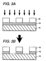
Fig. 3A and 3B are diagrams depicting in cross-section
two major steps in the manufacture of a
semiconductor wafer in accordance with a second
embodiment of the invention.
Fig. 4A and 4B are diagrams showing in cross-section
two major steps in the manufacture of a
semiconductor wafer in accordance with a third
embodiment of the invention.
DETAILED DESCRIPTION OF PREFERRED EMBODIMENTS
Some preferred embodiments of the dry cleaning
methodology of the present invention will be explained
in detail with reference to the accompanying drawings.
Fig. 1 illustrates a configuration of microwave
etching apparatus adapted for use in performing the
dry cleaning method in accordance with the present
invention. In this drawing, reference numeral 1
designates a silicon wafer (substrate) to be subjected
to microfabrication; numerals 3 and 4 denote a quartz
bell jar and a main chamber for establishment of the
vacuum environment required. 10 indicates an exhaust
port for vacuum evacuation whereas 15 denotes a gas
introduction section for introduction of a gas or
gases used in etching or dry cleaning. 9 is a
substrate stage for rigid support of a wafer under
manufacture; 8 is a clamper for clamping the wafer.
This clamper may typically be made of ceramics
including, but not limited to, alumina ceramics.
Electrostatic suction force may be used to rigidly
support the wafer on the substrate stage 9. 7
designates an Earth plate; 11 denotes a high-frequency
power supply for application of a radiofrequency (RF)
bias voltage between the Earth plate 7 and wafer stage
9.
The microwave etching apparatus shown herein is
first subject to introduction of a chosen gas for use
in generating a plasma after completion of high vacuum
evacuation. Then, microwaves 14 are excited by a
magnetron (not shown) and are then introduced via the
waveguide 5 into the quartz bell jar 3 (processing
room) causing a gas in the processing room to
transform into a plasma by electronic cyclotron
resonance (ECR) with a magnetic field as created by
the solenoid 6 disposed around the processing room,
which plasma is used to effectuate an intended etching
treatment. The RF bias voltage is applied by the high-frequency
power supply 11 between the Earth plate 7
and wafer stage 9 for the purpose of performing an
anisotropic etching by attraction of ions thereto.
At this time certain reaction products formed as
secondary products of the etching process can be
attached and stacked onto the constituent components
of the processing room, such as the quartz bell jar 3,
main chamber 4, exit 15 of the gas introduction
section, clamper 8 and others, which would result in
formation of more than one deposition film 13. As
wafers under processing increase in number letting
such deposition film 13 likewise increase in thickness,
this film behaves to peel off from the inner walls
then badly behaving as dusts or contaminants which can
cause pattern defects of resultant devices
manufactured.
Suppose for example that a silicon oxide film
(SiO2) 17 for use as a dielectric film shown in Fig. 2
(Fig. 2A and 2B) is etched using a plasma of
fluorocarbon-based gas-here, CF4 gas-and plasma of
additive gases of Ar and O2. As shown in this drawing
the SiO2 film 17 is formed on a substrate 16 by way of
example, and a mask pattern 18 made of a chosen
photoresist material is further formed thereon
allowing the resulting structure to be subject to an
etching treatment by use of the etching apparatus
shown in Fig. 1. At this time the etching gas attempts
to dissociate in the plasma hitting the target wafer
so that the etching progresses accordingly. When this
is done, any unnecessary deposits left adhered to the
inner walls of the apparatus with the to-be-etched
object being as the cause thereof may become oxides
containing silicon and chemical compounds containing
organic substance.
Incidentally, a gas used for dry cleaning is aimed
at creation of chemical compounds of increased vapor
pressure by reaction with the deposits to be removed
away, which will finally be removed through
vaporization and vacuum evacuation. Assuming for
instance that the deposits are carbon compounds, a
plasma of O2 gas is applied thereto permitting
vaporization thereof to CO or CO2 gases for removal.
To do this, the prior art approach as taught by PUJPA
No. 7-508313 indicated in the introductory part of the
description is designed to employ a cleaning gas
consisting of the mixture of a chlorine-based gas and
oxygen-based gas. Mixing oxygen thereinto may improve
the efficiency as a whole by disconnecting or
separating carbon from chemical compounds containing
therein metal and chlorine as well as organic
substance while cleaning the metal by chlorine.
When etching the SiO2 film as used in this
embodiment, cleaning is typically done using a mixture
or combination of a fluorine-based gas and oxygen-based
gas. However, as stated supra, the plasma
originated from the etching gas attempts, in addition
to etching the substrate surfaces 17, 18 to be etched,
to hit also the materials of apparatus internal parts
or components such as for example the clamper 8 and
Earth plate 7 resulting in an increase in amount of
undesired secondary etching products devotable to
creation of the deposition film 13, which products may
include in addition to the reaction products of the
to-be-etched material either the ion sputtered
products of the apparatus internal component materials
or chemical compounds of such apparatus materials and
of the etching gas used herein.
Typically, alumina components are employed in
plasma-applied semiconductor manufacturing apparatus
including the etching apparatus. In this embodiment
(the example shown in Fig. 2) unnecessary deposits
stacked or adhered to the apparatus inner walls may be
left in the form of organic compounds of the to-be-etched
SiO2 material and of resist material which are
originated from the to-be-etched object per se and
also in the form of alumina as a result of ion
sputtering due to the fact that the clamper 8 as one
of the alumina components inside the apparatus is hit
by a plasma. Part of this may be attached and adhered
in the form of aluminum fluoride by reaction of
fluorine during etching. The prior art dry cleaning
architecture merely comes with a cleaning treatment
with respect to limited materials such as SiO2 and
organic compounds of resist materials. To be more
specific, the prior art fails to take into
consideration in any way the depositability of either
sputtered products of the apparatus internal component
materials or chemical compounds of such apparatus
materials and etching gas; obviously, the prior art
does not take account of how a cleaning is to be done
therefor. Accordingly, these might be finally left as
the cause for generation of contaminants.
According to the present invention, it becomes
possible, by adding to the dry etching process both
the step of removing etching reaction products and the
step of removing any chemical compounds of the
apparatus inside component materials and etching
gas(es), to successfully remove away also the deposits
made of such compounds of the apparatus internal
component materials which have been long ignored in
the conventional dry cleaning technology, which in
turn leads to capability of improving the cleaning
effect while simultaneously increasing the contaminant
generation suppression effect.
The illustrative embodiment is specifically
designed to add as the apparatus inside material
cleaning treatment a cleaning step using a mixture gas
of BCl3 and Cl2. Aluminum attachments may be
effectively removed away by production of AlCl3 of high
vapor pressure using a Cl2 gas plasma. However, in
cases where such aluminum is of oxide or fluoride, the
plasma of Cl2 alone is incapable of producing AlCl3
rendering it impossible to effectuate any intended
removal by cleaning due to the fact that the
interatomic bonding energy of Al-O and Al-F remains
greater than the interatomic bonding energy of Al-C.
In view of this, a specifically arranged gas
containing therein B such as a BCl3 gas, which has its
interatomic bonding energy with respect to fluorine
and oxygen as greater in value than the interatomic
bonding energy of Al-O and Al-F, is mixed into the Cl2
gas thereby removing O and F out of Al-O and Al-F to
thereby render effective the cleaning by Cl2. This may
in turn enable achievement of successful removal of
ion sputtered products of the apparatus internal
component materials along with removal of inherent
etching reaction products.
Here, sequential execution of a cleaning using O2
and sulphur hexafluoride (SF6) and cleaning using a
mixture gas of BCl3 and Cl2 may remarkably increase the
cleaning effect inside the apparatus and also the
contaminant suppression effect therein.
In the way discussed above, the cleaning effect
within the apparatus may dramatically be improved by
performing the dry cleaning process for removal of ion
sputtered products of the apparatus internal member
materials or any chemical compounds of such apparatus
materials and an etching gas in addition to the dry
cleaning for removal of reactive products with respect
to the to-be-etched material. While in this embodiment
the dry cleaning for such etching reaction products
and the cleaning with respect to the apparatus
internal member materials are done sequentially, the
two cleaning gases may alternatively be mixed together.
Next, another embodiment applying the principles
of the present invention to tungsten lead wires will
be explained in conjunction with Fig. 3 ( Fig. 3A and
3B ). As shown in Fig. 3, a tungsten lead wire layer
19 is formed on the substrate 16 while a mask pattern
18 made of a chosen photoresistive material is formed
thereon; the resulting structure is then subject to an
etching process in the etching apparatus shown in Fig.
1. For such tungsten a plasma of SF6 gas is used to
facilitate progression of an etching required.
During the above process any unnecessary deposits
can be left adhered to the apparatus inner walls in
the form of chemical compounds containing therein
tungsten, fluorine and organic substance, and further
aluminum oxide as ion-sputtered during the clamper 8
that is one of the alumina components inside the
apparatus is being hit by a plasma. Part of this is in
the form of aluminum fluoride due to the plasma of SF6
gas during etching. Here, both the cleaning using SF6
and the cleaning using the mixture gas of BCl3 and Cl2
were done in a sequential manner. SF6 may exhibit some
cleaning effects with respect to tungsten and organic
substance also. The cleaning using the BCl3/Cl2 mixture
gas exhibits cleaning effects with respect to aluminum
oxide and aluminum fluoride as has been explained in
conjunction with the first embodiment. This cleaning
is advantageous in extremely improving the contaminant
suppression effect. As in the first embodiment, the
cleaning effect may be noticeably enhanced by
performing both the dry cleaning process for removal
of reaction products with respect to the etching
material and also the dry cleaning with respect to the
apparatus internal member materials.
An explanation will now be given of a further
embodiment incorporating the principles of the present
invention. Here, an exemplary case will be discussed
wherein the present invention is applied to the case
of etching aluminum lead wires as shown in Fig. 4 (Fig.
4A and 4B ).
Recently, most metal lead wires come with a
lamination structure having a barrier metal layer 21
associated therewith as depicted in Fig. 4, rather
than a single aluminum film structure, which permits
use of a plurality of kinds of etching gases during
etching processes thereof. This is for achieving
superior anti-electromigration characteristics and
diffusion barrier characteristics. Exemplarily
explained herein is the case of etching a lamination
film structure consisting essentially of an aluminum
lead-wire layer 20 and titanium-tungsten (TiW) barrier
metal 21. As stated previously, etching is performed
in a way such that a chosen chemical compound of high
vapor pressure relative to the material to be etched
is formed letting the etching progress. In this case
the first layer 20 made of aluminum is etched by
altering to AlCl3 of high vapor pressure using a Cl2
gas. When this is done, Al or AlClx can be attached
and adhered for deposition to the apparatus inner
walls, including several structure components of the
processing room, such as for example the quartz bell
jar 3, main chamber 4, gas introduction port 15, and
clamper 8. Thereafter, the second layer of TiW2O is
processed by a SF6 plasma; at this time, Ti or tungsten
(W) might be stacked and adhered to the apparatus
inner walls and/or the constituent components of the
processing room thereof.
Typically, in cases of cleaning Al or AlClx and of
cleaning Ti, the Cl2 plasma may be used for removal
thereof by altering them to AlCl3 and TiCl of higher
vapor pressure. In the case of cleaning W, a plasma of
fluoride gas, such as for example SF6 plasma, is
employable to remove the same by altering it to WF6 of
higher vapor pressure.
Unfortunately, in cases where the film for
configuration of an intended lead wire pattern is of
lamination film structure rather than a single film
structure, resultant deposition films left adhered to
the apparatus inner walls and the constituent
components of the processing room are not a simple
form but in the "complex" form of chemical compounds
with such gasses because of use of a plasma of plural
etching gases and also use of multiple cleaning gases.
More specifically, any possible additive deposits
are such that:
In the way discussed above, where a multi-layered
lead wire is to be etched, certain plasma of an
etching gas behaves during etching of one lead wire
layer to alter certain deposits as stacked to the
apparatus inner walls during etching of another lead
wire layer to specific chemical compounds hard to be
removed away. Furthermore, during cleaning deposits of
a certain element, the plasma of a cleaning gas used
herein attempts to alter those deposits of another
element to compounds hard to be removed. These can
disadvantageously serve to provide a bar to
accomplishment of intended cleaning performance.
Moreover, the plasma of etching gas and that of
cleaning gas will possibly hit the apparatus inside
materials also, which results in attachment of ion
sputtered products of such apparatus materials to
inside of the apparatus. These may also become
chemical compounds with the etching gas and cleaning
gas. These can raise a serious bar to achievement of
an intended cleaning in both performance and
reliability.
According to the present invention, the dry
cleaning process is specifically added with a cleaning
step using a specific gas containing therein a chosen
material having the interatomic bonding energy with
the etching gas elements which energy is greater in
value than the interatomic energy between the
element(s) constituting the to-be-etched object and
those constituting the etching gas. This makes it
possible to successfully remove any unnecessary
deposits as discussed at Paragraph 1). Specifically,
it becomes possible to remove away those aluminum
fluorides which are altered by SF6 plasma during the
TiW etching of the second layer from Al as deposited
during etching of the first layer.
Another advantage of the invention lies in
capability of removing the deposits discussed supra at
Paragraph 3) because of the fact that the step of
removing ion sputtered products of the apparatus
internal member materials is added along with the step
of removing etching reaction products. This in turn
makes it possible to remove any ion sputtered products
of aluminum components used as internal parts or
components of the etching apparatus employed.
Furthermore, the dry cleaning process is
specifically arranged to include a cleaning step using
a specific gas containing therein a material having
the interatomic bonding energy with the gas elements
of the cleaning step, which energy is greater in value
than the interatomic bonding energy between inherent
materials, including the to-be-etched material and
apparatus component materials, and the elements
constituting the cleaning gases at other steps. This
may advantageously serve to enable successful removal
of those deposits of the kinds as discussed at
Paragraphs 2) and 4) to 5). In other words, it becomes
possible to remove any deposits which have become
aluminum fluoride due to the SF6 plasma during the W
cleaning.
More practically, use of Cl2 plasma alone is unable
to remove by cleaning the aluminum fluoride which has
been created by alteration of aluminum to fluoride due
to the SF6 plasma as used during the etching and
cleaning. Arranging the dry cleaning process so as to
employ as the cleaning gas a mixture of Cl2 and BCl3
added thereto-the latter is a chosen gas containing
therein the material B having the interatomic bonding
energy with fluorine which energy is greater in value
than the interatomic bonding energy between fluorine
for use in etching and cleaning and aluminum used as
the to-be-etched material--may enable separation of F
from Al-F, which in turn renders effective the
cleaning using Cl2.
B is such that the interatomic bonding energy of
B-O is greater than that of aluminum oxide Al-O which
is the ion sputtered products of the apparatus
internal member material(s). Accordingly, mixing a B-contained
gas and BCl3 into Cl2 gas enables separation
of O from Al-O rendering more effective the cleaning
by Cl2. This makes it possible to remove any ion
sputtered products of the apparatus internal member
materials also.
The aforesaid cleaning process for certain the
films deposited by reaction with the etching and
cleaning gases at the next step as required due to the
multilayer lamination film structure may be performed
before and/or after the cleaning process for etching
reaction products alone.
It must be noted that although the illustrative
embodiments of the invention have been described based
on specific examples directed to use of the microwave
etching apparatus, the invention should not
exclusively be limited thereto and may alternatively
be modifiable for use in other applications with
etching apparatus of any type as far as it is designed
to employ a plasma to clean out deposits on the
apparatus inner walls, including but not limited to
parallel-flat plate type etching apparatus, induction-coupled
etching apparatus, or CVD apparatus, while
offering similar technical advantages discussed
previously.
As has been described above, according to the
present invention, it becomes possible to effectively
remove any deposition films left adhered to the inner
walls of manufacturing apparatus employed. This makes
it possible to eliminate peel-off or abruption of such
deposition films due to an increase in thickness
thereof (increase in processing number) and also dust
production as originated therefrom, which in turn
enables improvement of the production yield during
manufacturing processes while simultaneously
increasing the working efficiency of manufacturing
apparatus used.
While the invention has been described with
reference to specific embodiments, the description is
illustrative of the invention and is not to be
construed as limiting the invention. Various
modifications and applications may occur to those
skilled in the art without departing from the true
spirit and scope of the invention.