The present invention relates to a wiring
substrate having penetrating filled vias arranged in a
matrix-shape.
The inventors have previously invented a method
of making a substrate having via conductors which
penetrate the substrate. In the method large number of
fine metallic wires made of copper are arranged in a
container in parallel with the axis of the container.
This container is filled with a dispersed solution in
which ceramic powder such as alumina powder which is to be
fired at high temperature is dispersed. After drying,
ceramic powder is fired at high temperatures higher than
the melting point of the fine metallic wires so that the
ceramic powder fired at high temperatures can be sintered
sufficiently densely. In this way, a columnar sintered
body, which has been densely sintered, is obtained. This
sintered columnar body is sliced perpendicularly to the
axis, so that a substrate having via conductors which
penetrate the substrate can be obtained.
According to the above method, the fine metallic
wires are melted in the process of sintering the ceramic
powder at a high temperatures. Therefore, even if the
ceramic contracts in the process of sintering, the fine
metallic wires are not broken, and it is possible to make
a substrate having via conductors arranged densely in the
substrate. Also, it has been confirmed by the inventors
that the fine metallic wires are not diffused in the
ceramic.
Further, the inventors have develcped another
method of making a substrate having via conductors which
penetrate the substrate. In the method a large number of
fine metallic wires made of copper are arranged in a
container in parallel with the axis of the container.
This container is filled with ceramic powder which is to
be fired at low temperatures and the primary. component of
the ceramic powder is glass. The ceramic powder is fired
at a temperatures lower than the melting point of the fine
metallic wires. In this way, a columnar sintered body is
obtained. This sintered body is sliced perpendicularly to
the axis, so that a substrate having via conductors which
penetrate the substrate can be obtained.
According to the above method, ceramic powder,
which is to be fired at low temperatures and the primary
component of which is glass, is melted in the process of
sintering. Accordingly, stress is not applied to the fine
metallic wires. Therefore, it is possible to make a
substrate having via conductors which are not broken.
However, according to the former method, the
following problems may be encountered. Since the ceramic
fired at a high temperature contracts with a coefficient
of contraction of about 40%, the dimensional accuracy is
low. Further, since the ceramic is densely fired, the
hardness of the ceramics is very high. Therefore, it is
difficult to slice the sintered body. If any additive is
added to the ceramics so as to lower the hardness, the
mechanical strength would also be lowered.
According to the latter method, the following
problems may be encountered. In the latter method, a
ceramic fired at a low temperatures, the primary component
of which is glass, is used. Accordingly, the fired
ceramic is fragile, and the mechanical strength is low.
It is an object of the present invention to provide a
wiring substrate characterized in that: the core material
is commonly used, so that the manufacturing cost can be
reduced; and the above problems are solved and the
dimensional accuracy of the wiring substrate is high.
In order to accomplish the above object, the present
invention is composed as follows.
The present invention provides a wiring substrate
comprising: a core substrate; penetrating filled vias
formed on the core substrate, the diameters of the
penetrating filled vias being the same and not more than
300 µm, the penetrating filled vias being formed into a
matrix-shape at regular intervals of not more than 2 mm; a
plane pattern formed on a surface of the core substrate
through an insulating layer, the plane pattern having pad
portions; and connecting vias penetrating the insulating
layer, the connecting vias electrically connecting each
pad portion on the wiring pattern with each corresponding
via of the filled vias one to one, wherein a portion of
the filled vias are not connected with the wiring pattern.
When a standardized common core substrate is used,
which has penetrating filled vias of the same diameter of
not more than 300 µm and the penetrating filled vias are
arranged at regular intervals of not more than 2 mm, and
formed into a matrix-shape, it is possible to reduce the
manufacturing cost. The radiating property of the wiring
substrate is excellent because the fine metallic wires are
arranged in the core substrate.
When the filled vias not connected with the wiring
pattern are corrected with the grounding terminals, the
occurrence of cross talk can be decreased, and the
electrical characteristic can be improved.
According to the invention, the core substrate is
composed of a wiring body used for manufacturing a
substrate in which a large number of fine metallic wires
are embedded in parallel with the axis of a columnar body
which is made in such a manner that a porous fired
inorganic insulating material is impregnated with organic
insulating material, and the wiring body used for
manufacturing a substrate is sliced in a direction
perpendicular to the axis. Especially when the ceramic is
fired to be porous, it is possible to obtain a core
substrate, the hardness of which is not so high and it can
be easily machined, that is, it can be easily sliced. The
coefficient of contraction is very low. Therefore, the
dimensional accuracy of the via conductor is high. In
this connection, the inorganic insulating material has a
skeleton structure of a continuous phase. Therefore, the
mechanical strength is high.
One of the characteristics is that a ratio of the
inorganic insulating material is not lower than 50 volume
% and not higher than 80 volume %.
When the ratio of the inorganic insulating material
is lower than 50 volume %, it is difficult to set the
condition of firing, and the porosity varies. Therefore,
the reproducibility is deteriorated. When the ratio of
the inorganic insulating material is approximately 60%,
contraction seldom occurs in the process of firing, and
the dimensional accuracy is high. When the ratio of the
inorganic insulating material is higher than 80%, the
density is somewhat increased, and contraction is caused.
Therefore, problems may be caused in the dimensional
accuracy. Further, some of the blow holes in the
inorganic insulating material are impregnated with resin
and become discontinuous.
The incrganic insulating material is preferably made
of a fired body of aluminum oxide, mullite, cordierite or
aluminum nitride.
In the process of firing, necks are generated among
powder. Therefore, it is possible to obtain a porous
fired body in which powder is connected with each other.
Alternatively, the inorganic insulating material may
be a mixed fired body in which glass, the softening point
of which is not higher than 1000°C, is mixed with one or
more of aluminum oxide, mullite, cordierite, silicon
oxide, aluminum nitride, silicon carbide and silicon
nitride.
In the process of firing, the glass component
connects the ceramic powder. Therefore, contraction can
be suppressed without conducting sintering.
The organic insulating material may be a resin of
polyimide, benzocyclobutene, bismaleimide triazine, epoxy
or polyphenylene ether.
The heat resistance of a resin of polyimide or
benzocyclobutene is high.
A wiring body is used for manufacturing a substrate
in which a large number of fine metallic wires are
embedded in a columnar body composed of an organic
insulating material of continuous phase and an inorganic
insulating material of discontinuous phase, in parallel
with the axis of the columnar body.
In this case, since the inorganic insulating material
is dispersed in the organic insulting material,
contraction seldom occurs, and the dimensional accuracy is
high and the mechanical strength is high. Further, it is
possible to reduce the manufacturing cost.
In this case, it is preferable that a ratio of the
organic insulating material is not lower than 3C volume %
and not higher than 60 volume %.
When the ratio of the organic insulating material is
lower than 30 volume %; it becomes difficult to mix the
inorganic insulating material with the organic insulating
material. When the ratio of the organic insulating
material is higher than 60 volume %, there is a
possibility that the mechanical strength is deteriorated.
It is preferable that the inorganic insulating
material is one or more of aluminum oxide, mullite,
cordierite, silicon oxide, aluminum nitride, silicon
carbide and silicon nitride. Especially when aluminum
nitride is used for the inorganic insulating material, it
is possible to make a wiring substrate the radiating
property of which is excellent.
Particular examples in accordance with this invention
will now be described with reference to the accompanying
drawings, in which:-
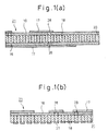
Fig. 1(a) is a cross-sectional view for explaining
the wiring substrate 21 according to the present
invention.
Reference numeral 20 is a core substrate manufactured
by various manufacturing methods described later. Filled
vias 18 composed of fine metallic wires, the diameters of
which are the same and not larger than 300 µm, are
arranged in the insulating material of the core substrate
20 in such a manner that the filled vias 18 penetrate the
core substrate 20 in the vertical direction and are formed
into a matrix-shape at regular intervals of not more than
2 mm.
In this case, it is preferable to use a standardized
core substrate 20 in which the diameter of the filled via
18 is, for example, 300 µm, 200 µm, 100 µm or 50 µm, and
the interval between the filled vias 18 is, for example, 2
mm, 1.5 mm, 1.27 mm, 1 mm or 0.5 mm.
In this connection, unless the diameter of the filled
via 18 (fine metallic wire) is a value not less than 50
µm, there is a possibility of breaking of the wire when
the columnar body is formed.
On both surfaces of the core substrate 20, there are
provided insulating layers 16, 16 made of insulating
material such as photosensitive resist. The insulating
layers 16, 16 may be formed in such a manner that resin
sheets are made to adhere onto the surfaces of the core
substrate 20 with adhesive. Alternatively, the insulating
layers 16, 16 may be formed in such a manner that a
varnish-like resin is coated on the surfaces of the core
substrate 20.
Through-holes 26 are formed on the insulating layers
16, 16 in accordance with a predetermined pattern so that
the predetermined filled vias 18 can be exposed. These
through-holes 26 may be formed by the method of
photolithography. Alternatively, these through-holes 26
may be formed by means of laser beams in the case where
the insulating layers 16 are not a photosensitive resist.
These through-holes 26 are filled with conductive
material such as conductive resin, so that the connecting
vias 28 can be formed.
On the surfaces of both insulating layers 16, 16, the
predetermined plane wiring patterns 17, 17 are formed so
that they can be connected with the connecting vias 28.
In this way, the wiring substrate 21 is formed.
The wiring patterns 17, 17 are formed as follows.
Thin metallic films made of copper are formed on the
insulating layers 16, 16 by means cf sputtering or vapor-deposition.
If necessary, plating is conducted on the
thin metallic films. In this way, a thin metallic film of
a predetermined thickness is formed. After that, the thin
metallic film is subjected to etching. In this way, the
wiring patterns 17, 17 can be formed.
Alternatively, layers of metallic foil such as
electrolysis copper foil may be previously provided on the
insulating layers 16, 16. Through-holes 26 are formed at
the predetermined positions on the insulating layers 16,
16 having layers of metallic foil. These through-holes 26
are filled with conductive material so as to form the
connecting vias 28. The thus formed insulating layers 16,
16 are made to adhere onto both surfaces of the core
substrate 20. Then, the layers of metallic foil are
etched, so that the predetermined wiring patterns 17, 17
can be formed. Alternatively, when the insulating layers
are in the stage of sheets, the layers of metallic foil
may be previously etched so as to form the wiring patterns
17, 17. After that, the insulating layers may be made to
adhere onto the core substrate 20 so as to form the wiring
substrate 21.
Concerning the core substrate 20 described above, the
filled vias 18 are previously formed into a matrix-shape
on the core substrate 20 in accordance with the
standardized diameter and interval of the matrix. When
the thus standardized core substrate 20 is used, the
manufacturing cost can be reduced.
When the wiring patterns 17, 17 are designed, it is
possible to conduct free designing by effectively using
the filled vias 18 which are arranged in a matrix-shape.
Of course, there are filled vias 18 which are not
used. Even when these vias 18 which are not used exist,
they have no adverse effect on this wiring substrate.
When the filled vias 18 are densely formed, the heat radiating
property can be improved by these vias.
In this connection, the filled vias 18 which are not
used may be connected with grounding terminals (not shown)
formed on the surface of the core substrate 20. In this
way, the filled vias 18 can be put into use.
When a portion of the filled vias 18 are used for
grounding, the grounding vias are mixedly provided between
the signal lines. Therefore, the occurrence of cross-talk
between the signal lines can be advantageously prevented.
In this embodiment, each signal line and the power
source line provided between the wiring patterns 17, 17
are electrically connected through one corresponding
filled via 18. When the standardized filled via 18 of a
predetermined size is used, the via resistance can be
decreased.
In the embodiment shown above, the wiring substrate
21 having only one layer is shown as an example. Of
course, it is possible to provide a plurality of layers on
the wiring substrate.
Fig. 1(b) is a view showing another embodiment of the
wiring substrate 21. Like reference characters are used
to indicate like parts in this embodiment and the
embodiment explained before with reference to Fig. 1(a).
In this embodiment, the plane wiring pattern 17 is
formed only on one side of the core substrate 20 through
the insulating layer 16, and on the other side of the core
substrate 20, the lands 27 electrically connected with the
filled vias 18 are directly formed on the surface of the
core substrate 20.
It is possible to form this wiring substrate 21 in
the same manner as that described before. Alternatively,
the wiring substrate 21 can be formed as follows.
First, a non-electrolytic copper plating layer is
formed on one surface of the core substrate 20 obtained in
the manner described later. Next, an epoxy bonding sheet
is made to adhere onto the reverse side of the core
substrate 20 and cured, so that an insulating layer 16 can
be formed.
Holes 26, the bottom surfaces of which are the end
faces of the filled vias 18, are formed at predetermined
positions on the insulating layer 16 by means of laser
beams of CO2. Then, electrolytic copper plating is
conducted in which the non-electrolytic copper plating
layer is used as an electrode, so that the holes 26 are
filled with copper. In this way, the connecting vias 28
can be formed.
Successively, a plane wiring pattern 17 connected
with the connecting vias 28 is formed on the insulating
layer 16 by the semi-additive method, and the non-electrolytic
copper plating layer on the reverse side of
the core substrate 20 is etched, so that the lands 27
connected with the end surface of the filled via 18 are
formed. In this way, the wiring pattern 21 can be
provided.
In this connection, the insulating layer 16 may be
formed by coating photosensitive epoxy resin on the core
substrate 20, and holes 26 may, be formed at predetermined
positions on the insulating layer 16 by the photo-process
in which the end surface of the filled via 18 is used as
the bottom surface. The thus formed holes 26 are filled
with copper. In this way, the connecting vias 28 may be
formed.
Figs. 2 to 4 are views showing examples of the
semiconductor device 30 in which the above wiring
substrate 21 is used.
In the example shown in Fig. 2, the semiconductor
chip 15 is connected to by means of flip chip process and
mounted on one wiring pattern 17 and external connecting
terminals 19 composed of solder bumps are attached onto
the other wiring pattern 17. In this way, the
semiconductor device 30 of a BGA (ball grid array) type is
formed. The filled vias 18 which are not connected with
the signal line and the power source line are connected to
the grounding terminals.
In this connection, reference numeral 23 is a resin
used for sealing .
The insulating layer 16 functions as a buffer layer
between the core substrate 20 and the semiconductor chip
15.
In the example shown in Fig. 3, there is shown an
example in which the semiconductor chip 15 is mounted on
the radiating plate 25 arranged at the center of the core
substrate 20. The semiconductor chip 15 and the wiring
pattern 17 are electrically communicated with each other
by a wire.
Other points are the same as those shown in Fig. 2.
In the example shown in Fig. 4, the radiating plate
25 is attached onto one side of the core substrate 20 so
that the through-hole formed at the center of the core
substrate 20 can be covered with the radiating plate 25,
and the semiconductor chip 15 is mounted on this radiating
plate 25. Other points are the same as those shown in
Fig. 3.
Successively, the core substrate 20 and the method of
manufacturing it will be explained below.
Fig. 5 is a cross-sectional view showing an outline
of the columnar body 10 which is a wiring body used for
manufacturing a substrate.
Reference numeral 12 is an inorganic insulating
material which has been fired into a porous columnar body.
Reference numeral 14 is a large number of fine metallic
wires made of copper or aluminum which are embedded in the
inorganic insulting material 12 in parallel with the axis.
The porous inorganic insulating material 12 is
impregnated with the organic insulating material 13 (shown
in Fig. 6).
When this columnar body 10 is sliced perpendicularly
to the axis and to an appropriate thickness, it is
possible to obtain a core substrate (shown in Fig. 7)
having the filled vias 18 in which the fine metallic wires
penetrate.
The organic insulating material 13 may be a resin
selected from polyimide, benzocyclobutene, bismaleimide
triazine, epoxy or polyphenylene ether.
The resin of polyimide or benzocyclobutene is
recommended for its heat resistance.
In order to impregnate the above resin into the
inorganic insulting material 12, first, the inorganic
insulating material is impregnated with a coupling agent
such as a silane coupling agent in a decompressed
condition so that the inorganic insulating material can be
closely contacted, and then the coupling agent is replaced
with the above resin which is in a varnish-like condition,
and after that, the resin is cured.
It is preferable that the inorganic insulating
material 12 is made by firing a ceramic powder, which is
to be fired an high temperatures, of one of aluminum
oxide, mullite, cordierite and aluminum nitride.
The columnar body 10, which has been made by firing
the above ceramic powder fired at high temperatures, is
porous as shown in the cross-sectional view of Fig. 6, and
the void portions are open to the surface and formed into
a continuous phase. In this connection, a portion may be
a closed void portion. That is, firing is conducted so
that the ceramic powder fired at high temperatures cannot
be made dense.
A ratio of the volume of the inorganic insulating
material to the overall volume of the columnar body 12 is
preferably 50 to 80%. When the volume of the inorganic
insulating material is lower than 50 volume %, it is
difficult to set the firing condition, and the porosity
varies. As a result, the reproducibility is deteriorated.
When the volume of the inorganic insulating material is
approximately 60 volume %, contraction seldom occurs in
the process of firing, and it is possible to enhance the
dimensional accuracy. When the volume of the inorganic
insulating material becomes higher than 80 volume %, the
ceramic powder is somewhat made dense, and contraction is
caused. Therefore, the dimensional accuracy is
deteriorated. Further, some of the blow holes (voids) may
be discontinued, and it becomes impossible to impregnate a
pcrtion of the inorganic insulating material with resin.
On the other hand, when a ratio of the incrganic
insulating material 12 to the crganic insulating material
13 is adjusted, the coefficient of thermal expansion, the
coefficient of thermal conductivity and the dielectric
constant of the core substrate 20 can be advantageously
controlled.
In general, the density of a ceramic fired body
depends upon the firing temperature, firing time and
distribution of grains in powder. The firing condition is
determined so that the surfaces of ceramic grains can be
liquidized and the liquidized surfaces adjacent to each
other can be made to adhere to each other when neck
portions are formed between them (shown in Fig. 6). In
this way, the firing condition is determined so that the
ceramic fired body cannot be made dense.
The principle by which the ceramic fired body is made
dense is described as follows. First, the grains adjacent
to each other form neck portions. When firing is
continued, surface energy acts on the grains so that the
surface area can be decreased. By this surface energy,
the grains grow to a large size.
In this embodiment, firing is stopped before the
surface energy to grow the grains is generated.
Accordingly, the firing temperature is set at a value
lower than the temperature at which the ceramic powder is
made dense, and further the firing time is generally
shortened, and furthermore the grain size is made to be
somewhat large. In this case, the grain size distribution
is not so important. That is, the firing condition need
not be very accurate, and manufacturing can be easily
performed.
In this embodiment, while the porosity of ceramic
powder is maintained high, firing is executed. Therefore,
it is possible to suppress the ratic of contraction in the
process of firing.
It is preferable that the ratio of contraction is
maintained at a value not higher than 1%. It is easy to
maintain the ratio of contraction at a value not higher
than 5%.
Consequently, the dimensional accuracy of the core
substrate 20, which has been cut out from the fired
ceramic body, is high. Specifically, it is possible to
obtain a core substrate 20 in which the dimensional
accuracy of the filled vias 18 is high.
The hardness of the fired body of this embodiment is
not higher than that of a fired body which has been made
dense. Accordingly, slicing can be easily conducted with
a cutter, and the production efficiency can be increased.
In this embodiment, a body, which has not been fired,
is made from a dispersed solution in which slurry-like or
paste-like ceramic powder is dispersed. Accordingly, it
is pcssible to use a dispersed solution in which no
organic binder is used or only a small quantity of organic
binder is used, in which slurry-like or paste-like ceramic
powder (inorganic insulating material) is dispersed. The
thus obtained dispersed solution is poured into a
container 6 in which fine metallic wires 14 are stretched
in parallel with each other between the upper wire guide 2
and the lower wire guide 4 as shown in Fig. 8. After
that, the poured dispersed solution is dried. In this
way, a ceramic powder body, which has not been fired, is
provided.
Since an organic binder is not used as described
above, it is unnecessary to remove the organic binder in
the firing process. Accordingly, it was possible to fire
a sufficiently thick body (columnar body) in a short
period of time. For example, it was possible to fire a
columnar body, the diameter of which was 10 cm and the
height of which was 20 cm, in about 4 hours. Due to the
foregoing, the productivity was greatly enhanced.
On the other hand, if an organic binder is used, it
becomes necessary to remove the organic binder in the
process of firing. For example, if a green sheet is used,
and if it is thick, the binder cannot be sufficiently
removed from a thick body. Therefore, it is possible to
fire only a thin body, the thickness of which is
approximately 3 cm at most.
Fine metallic wires 14 may be made of copper, gold or
aluminum.
These fine metallic wires may be melted or not melted
in the process of firing the inorganic insulating material
12.
Since firing is conducted under that condition that
the inorganic insulating material 12 seldom contracts in
the process of firing, that is, since firing is conducted
under that condition that the inorganic insulating
material 12 is not made dense, even if the fine metallic
wires 14 are not melted, there is no possibility of
breaking of the wires and deformation of the fired body
caused by the contraction of the inorganic insulating
material 14.
In this connection, when the fine metallic wires 14
are melted, it is possible to consider a case in which the
conductive metal disappears by the vaporization or
permeation of the liquidized metal into the ceramics, and
also it is possible to consider a case in which the fine
metallic wires 14 are short-circuited. However,
concerning the vaporization of the melted metal, it is
possible to take countermeasure by coating an end portion
of the body, which has not been fired yet, with ceramic
paste or slurry. Concerning the permeation or diffusion
of the liquidized metal into the ceramic, it was confirmed
by the inventors that no permeation or diffusion of the
melted metal into the ceramic actually occurred.
From the viewpoint of reduction of the manufacturing
cost, it is advantageous to conduct firing in the
atmosphere.
According to the result of the confirmation made by
the inventors, when the fine metallic wires were made of
copper, copper was oxidized in the atmosphere. Therefore,
it is necessary to conduct firing in a non-oxidizing
atmosphere.
When the fine metallic wires 14 were made of
aluminum, it was estimated that aluminum was also
oxidized. However, the result of the confirmation was
that aluminum was not oxidized contrary to the estimation.
Formation of oxide film was recognized on the surface of
the fine metallic wires of aluminum It was considered
that this oxide film of aluminum functioned as a barrier,
so that the intrusion of oxygen into the center could be
prevented by the oxide film of aluminum. As a result,
when the fine metallic wires were made of aluminum, it was
possible to conduct firing in the atmosphere at low cost,
and no problems were caused in the electrical continuity.
Fig. 9 is a view showing another embodiment of the
columnar body 10.
The structure of this embodiment is the same as that
of the above embodiment. In the columnar body 10 of this
embodiment, there are provided fine metallic wires 14, and
further there are provided rod-shaped bodies 22 in
parallel with the axis of the columnar body 10, wherein
the rod-shaped bodies 22 are made of a ceramic such as
aluminun nitride, a metal such as copper, or a compound
material composed of ceramic and metal, so that the
radiating property of rod-shaped body 22 is excellent.
In order to obtain the above columnar body 10, of
course, the rod-shaped body may be arranged in the
container 6 shown in Fig. 8 together with the fine
metallic wires 14. These circumstances are not shown in
the drawing.
Fig. 10 is view showing an embodiment in which the
above columnar body 10 is sliced with a cutter to an
appropriate thickness so that the core substrate 20 is
formed.
It is possible to mount a semiconductor chip on the
radiating body 25 formed by slicing the rod-shaped body
22. Due to the foregoing, it is possible to provide a
core substrate, the radiating property of which is
excellent.
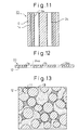
Fig. 11 is a view showing a still another embodiment.
The structure of this embodiment is the same as that
of the above embodiment. In the columnar body 10 of this
embodiment, there are provided fine metallic wires 14, and
further there are provided cylindrical bodies 24 made of
ceramics or metal, the section of which is square or
circular.
In order to obtain the above columnar body 10, the
cylindrical bodies 24 may be arranged in the container 6
together with the fine metallic wires 14 and then fired.
Fig. 12 is a view showing an embodiment in which the
above columnar body 10 is sliced with a cutter to an
appropriate thickness so that the core substrate 20 is
formed. Due to the foregoing, it is possible to provide
the core substrate 20 having through-holes 24a.
In this connection, the cylindrical bodies 24 may be
left as they are. Alternatively, the cylindrical bodies
24 may be drawn out at an appropriate stage in the
manufacturing process. In the case of drawing out the
cylindrical bodies 24 in the manufacturing process, it is
possible to form the through-holes using rod-shaped
bodies.
The thus obtained core substrate 20 can be used for
the semiconductor device shown in Fig. 4.
A ceramic to be fired at high temperatures is used
for the inorganic insulating material in the above
embodiments. Alternatively, the inorganic insulating
material may be a mixed fired body in which glass, the
softening point of which is not higher than 1000°C, is
mixed with one or more of the ceramics, to be fired at
high temperatures, of aluminum oxide, mullite, cordierite,
silicon oxide, aluminum nitride, silicon carbide and
silicon nitride.
In the mixed fired body described above, the glass
component is melted at low temperatures, and ceramic
powder is wetted by the melted glass component.
Therefore, ceramic grains are made to adhere to each
other. Therefore, it is possible to fire at lower
temperatures.
Fig. 13 is an enlarged cross-sectional view for
explaining a columnar body or substrate of this
embodiment. As can be seen in the drawing, particles of
the inorganic insulating material (ceramic particles) 12
are connected with each other by the melted glass
components 11. Therefore, voids are formed among the
particles of the inorganic insulating material particles.
The same resin 13 (organic insulating material) as that
described before is impregnated into the above voids. In
this way, the columnar body is completed. This columnar
body is sliced, so that the same substrate as that
described before can be provided.
According to this embodiment, it is possible to
suppress a ratio of contraction. Therefore, it is
possible to effectively manufacture a columnar body or
substrate of high dimensional accuracy.
Concerning the glass component 11, as long as it can
be sufficiently liquidized at the firing temperature, any
composition may essentially be used. However, it is
preferable to use crystalized glass, the primary component
of which is borosilicate or CaO-BaO-SiO2, or
alternatively, it is preferable to use non-crystalized
(amorphous) glass as a primary component.
In the above embodiment of the core substrate 20, the
porous fired Inorganic insulating material 12, the phase
of which is continuous, is impregnated with the organic
insulating material 13, the phase of which is continuous.
Further, a columnar body 10 is obtained in which a large
number of fine metallic wires 14 are embedded in parallel
with the axis. The thus obtained columnar body 10 is
sliced in a direction perpendicular to the axis.
In another embodiment of the core substrate 20, the
organic insulating material of the continuous phase is
provided, in which the inorganic insulating material made
of inorganic powder is dispersed as a discontinuous phase.
Further, a columnar body is obtained in which a large
number of fine metallic wires are embedded in parallel
with the axis. The thus obtained columnar body is sliced
in a direction perpendicular to the axis.
The organic insulating material may be a resin
selected from polyimide, benzocyclobutene, bismaleimide
triazine, epoxy or polyphenylene ether.
The heat resistance of resin of polyimide or
benzocyclobutene is high.
It is preferable that the inorganic insulating
material is one or more of aluminum nitride, siliccn
carbide, silicon nitride, aluminum oxide, mullite,
cordierite, and silicon oxide.
In order to mix the inorganic insulating material
with the above organic insulating an material, an
inorganic insulating material powder is dipped in a
coupling agent such as a silane coupling agent, so that
the coupling agent can be made to adhere onto the surface
of the inorganic insulating material, and then it is mixed
with the varnish-like organic insulating material.
When the coupling agent is made to adhere onto the
surface of the inorganic insulating material, the
inorganic insulating material and organic insulating
material can be excellently mixed with each other.
Especially when a large quantity of inorganic
insulating material is mixed with the organic insulating
material, it is necessary to conduct a pretreatment, on
the inorganic insulating material, with a coupling agent.
When the organic insulating material is cured after
mixing the organic insulating material with the inorganic
insulating material, the columnar body can be provided.
A preferable compounding ratio of the inorganic
insulating material is not lower than 35 volume % and not
higher than 60 volume %.
The higher the compounding ratio of the inorganic
insulating material is, the higher the entire mechanical
strength is increased. However, when the compounding
ratio of the inorganic insulating material exceeds 60
volume %, a compounding ratio of the organic insulating
material, which functions as a binder, is reduced.
Accordingly, it becomes difficult to mix the inorganic
insulating material with the organic insulating material.
When the compounding ratio of the inorganic insulating
material is lower than 35 volume %, the mechanical
strength becomes insufficient.
In this connection, when a large quantity of
inorganic insulating material is compounded, a relatively
large grain size of the inorganic insulating material is
advantageous, because the inorganic insulating material
can be excellently mixed with the organic insulating
material. Then the grain size of the inorganic insulating
material is large, the mechanical strength can be
enhanced. A preferable grain size of the inorganic
insulating material is approximately 40 µm or more.
In the same manner as that described before, the fine
metallic wires may be made of copper, gold or aluminum.
In order to manufacture the above columnar body, the
varnish-like organic insulating material and the inorganic
insulating material are mixed with each other to prepare
the material. The thus prepared material is poured into
the container 6 in which the fine metallic wires 14 are
stretched in parallel with each other between the upper
wire guide 2 and the lower wire guide 4 as shown in Fig.
8. Thus poured material is heated, so that the organic
insulating material can be cured.
Consequently, manufacturing is very easy, and a
sufficiently thick columnar body can be manufactured in a
short period of time. Due to the foregoing, the
productivity was greatly enhanced.
The thus obtained columnar body or the substrate is
seldom contracted. Therefore, the dimensions are seldom
varied by the contraction of the columnar body or the
substrate. It is possible to obtain a columnar body or
substrate, the dimensional accuracy of which is high.
In this connection, it is preferable to stop curing
the organic insulating material at stage B, that is, it is
preferable to stop curing the organic insulating material
in a tack dry condition. In order to complete curing at
stage B, a curing agent of aromatic polyamine may be used.
When curing is stopped at stage B as described above,
the substrate easily exhibits an adhesive property when it
is heated. Accordingly, the thus formed substrate is
preferably used for a multi-layer substrate.
EXAMPLE 1
Ethanol of 50 weight parts and surface active agent
of 0.1 weight parts were added to compound material of 100
weight parts, the composition of which was powder of
aluminum oxide of 50 weight % and glass of CaO-BaO-SiO2 of
50 weight %, the softening point of which was
approximately 850'C. Then the thus obtained mixture was
mixed with a ball mill for 20 hours, and a dispersed
solution was obtained.
The thus obtained dispersed solution was filled into
a container made of stainless steel in which copper wires,
the diameter of which was 0.3 mm, were stretched between
the upper and the lower wire guide plate, and then dried.
Then, the container fired at the maximuim temperature
of 960°C in dry nitrogen gas for 1 hour.
A porosity of the thus obtained fired body was
approximately 34%, and a ratio of contraction was
approximately 0.6%.
After this fired body had been treated in a coupling
agent, it was impregnated with a mixture, in which a
curing agent was compounded in epoxy of bisphenol, by the
vacuum substitution method, and step treatment was
conducted at the temperatures of 60, 80 and 150°C, so that
it was cured.
The obtained columnar body was sliced perpendicularly
to the axis, and a core substrate having vias, the
thickness of which was approximately 0.7 mm, was obtained.
Next, wiring patterns of copper were formed on both
sides of this core substrate by the additive method. It
was confirmed that a ratio of electrical communication of
each wire arranged between both sides of the substrate
through the substrate was 100%.
When powder of mullite, cordierite, silicon oxide,
aluminum nitride, silicon carbide or silicon nitride was
singly used instead of powder of aluminum oxide or
alternatively some of them were mixed with each other
instead of powder of aluminum oxide, substantially the
same effect was provided.
When glass of borosilicate, the softening point of
which was approximately 640°C, was used instead of glass
of CaO-BaO-SiO2, substantially the same effect was
provided.
Further, when a resin of polyimide, benzocyclobutene
or bismaleimide triazine was used instead of epoxy resin
of bisphenol, it was possible to provide the same
excellent effect as that described above.
When fine wires of gold or aluminum were used for the
fine metallic wires, the same effect was obtained.
A non-electrolytic copper plating layer was formed on
one side of the thus obtained core substrate, and then a
bonding sheet of epoxy was made to adhere onto a reverse
side of the core substrate and then cured so as to form an
insulating layer.
Holes, the bottom surfaces of which coincide with the
end surfaces of the filled vias, were formed at
predetermined positions on this insulating layer by means
of CO2, laser beams and electrolytic copper plating was
conducted using the above non-electrolytic copper plating
layer as an electrode, so that the holes were filled with
copper. In this way, the connecting vias were formed.
Next, a plane wiring pattern connected with the
connecting vias was formed on the insulating layer by the
semi-additive method, and the non-electrolytic copper
plating layer on the reverse side of the core substrate
was etched, so that the lands connected with the end
surfaces of the filled vias were formed. In this way, a
wiring substrate was made.
EXAMPLE 2
Ethanol of 50 weight parts and surface active agent
of 0.1 weight parts were added to compound material of 100
weight parts, the composition of which was powder of
aluminum oxide of 90 weight % and sintering assistant of
the residue composed of silicon dioxide, calcium carbonate
and magnesium oxide, and it was crushed and mixed with a
ball mill for 48 hours. In this way, a dispersed solution
was obtained.
The thus obtained dispersed solution was filled into
a container made of stainless steel in which copper wires,
the diameter of which was 0.3 mm, were stretched between
the upper and the lower wire guide plate, and then dried.
Then, the container was fired at the maximum
temperature of 1200°C in dry nitrogen gas for 30 minutes.
A porosity of the thus obtained fired body was
approximately 33%, and a ratio of contraction caused by
firing was approximately 1.5%.
After this fired body had been treated in an acid and
a coupling agent, it was impregnated with a resin and
cured in the same manner as that of Example 1. The thus
obtained body was sliced, and copper wires were formed on
both sides. Then, it was confirmed that a ratio of
electrical communication of each wire arranged between
both sides of the substrate through the substrate was
100%.
When powder of mullite, cordierite or aluminum
nitride was used instead of powder of aluminum oxide,
substantially same the effect was provided.
Using the thus obtained core substrate, a wiring
substrate was obtained in the same manner as that of
Example 1.
EXAMPLE 3
Ethanol of 80 weight parts and surface active agent
of of 0.1 weight parts were added to compound material of 100
weight parts, the composition of which was powder of
aluminum nitride of 50 weight parts and powder of
borosilicate glass of 100 weight parts, the softening
point of which was 825'C, and it was crushed and mixed
with a ball mill for 20 hours. In this way, a dispersed
solution was obtained.
This dispersed solution was filled into a cylindrical
container made of graphite or Boron Nitride in which
copper wires, the diameter of which was 0.3 mm, were
stretched between the upper and the lower wire guide plate
and further a rod of nylon, the diameter of which was 14
mm, was placed. The dispersed solution was dried and then
the rod of nylon was drawn out.
Then, the container fawns fired at the maximum
temperature of 850'C in dry nitrogen gas for 1 hour. A
porosity of the thus obtained fired body was approximately
38%, and a ratio of contraction in the radial direction
was approximately 0.3%.
After this fired body had been treated in a coupling
agent of silane, it was impregnated with a varnish of
polyimide by the vacuum substitution method and heated and
cured at the maximum temperature of 180°C.
When a varnish of benzocyclobutene, bismaleimide
triazine, epoxy or polyphenylene ether was impregnated
instead of a varnish of polyimide, the same good columnar
body as that described before was obtained.
The thus obtained columnar body was sliced in the
same manner as that of Example 1, and a core substrate
having vias, on which through-hole were formed, were
obtained.
Using the thus obtained core substrate, a wiring
substrate was obtained in the same manner as that of
Example 1.
EXAMPLE 4
Instead of the rod of nylon, the diameter of which
was approximately 14 mm, a rod of aluminum nitride, the
diameter of which was substantially the same, was used,
and even after the completion of drying, it was put into
use as it was. Except for that, other points were the
same as those of Example 3, that is, a columnar body was
obtained in the same composition and condition as those of
Example 3.
The thus obtained columnar body was sliced. In this
way, a core substrate having vias was obtained in which
penetrating bodies of ceramics of aluminum nitride were
formed. After polishing, a layer of titanium, the
thickness of which was approximately 0.1 µm, and a layer
of copper, the thickness of which was approximately 1 µm,
were formed by means of magnetron spattering. After that,
a layer of copper, the thickness of which was
approximately 2 µm, a layer of nickel, the thickness of
which was approximately 1 µm, and a layer of gold, the
thickness of which was approximately 1 µm, were formed by
means of electrolytic plating, and then etching was
conducted so as to form a wiring pattern. It was
confirmed that both surfaces were electrically
communicated through the substrate, and also it was
confirmed that the surface of the ceramic of aluminum
nitride and the compound surface of polyimide were
electrically communicated.
Using the thus obtained core substrate, a wiring
substrate was obtained in the same manner as that of
Example 1.
EXAMPLE 5
A powder of aluminum nitride, the average particle
size of which was approximately 40 µm and the surfaces of
which were cured, was subjected to surface hydrophobic
treatment by a silane coupling agent. A mixture of 20
weight parts, in which DDSA (dodecanal succcinic
anhydride), MNA (methylnadic anhydride) and DMP-30 (2.4.6-tris
(dimethyl aminoethyl) phenol) were compounded on the
base of epoxy of bisphenol, was added to and mixed with
the thus obtained powder of 80 weight parts. After that,
defoaming was conducted.
The thus obtained dispersed solution was filled into
a cylindrical container in which copper wires, the
diameter of which was 0.3 mm, were stretched between the
upper and the lower wire guide plate, and then dried when
it was treated stepwise at the temperatures of 60, 80 and
150°C.
The thus obtained columnar body was sliced in a
direction perpendicular to the primary axis of the
columnar body. In this way, a substrate having vias, the
thickness of which was approximately 0.7 mm, was obtained.
Using the thus obtained core substrate, a wiring
substrate was obtained in the same manner as that of
Example 1.
EXAMPLE 6
A solution of methylethylketone of 25 weight parts
containing a condensation type polynuclear aromatic resin
of 60 weight % was added to and mixed with powder of 85
weight parts obtained when spherical powder of alumina,
the average diameter of which was approximately 60 µm, was
subjected to surface hydrophobic treatment by a coupling
agent of silane, and then vacuum defoaming was conducted.
The thus obtained dispersed solution was filled into
a cylindrical container in which copper wires, the
diameter of which was 0.3 mm, were stretched between the
upper and the lower wire guide plate and a column of
aluminum nitride, the diameter of which was approximately
12 mm, was arranged, and then dried when it was treated
stepwise at the temperatures of 100 and 230'C.
The thus obtained columnar body was sliced in a
direction perpendicular to the primary axis of the
columnar body. In this way, a core substrate having vias
and radiating sections, the thickness of which was
approximately 0.7 nm, was obtained.
When spherical powder was used as described above,
powder could be filled more densely, so that the
mechanical strength of the substrate could be enhanced.
Using the thus obtained core substrate, a wiring
substrate was obtained in the same manner as that of
Example 1.
EXAMPLE 7
A polyimide varnish of 25 weight parts was added to
and mixed with powder of 80 weight parts obtained when
powder of mullite, the average diameter of which was
approximately 40 µm, was subjected to surface hydrophobic
treatment by a coupling agent of silane, and then vacuum
defoaming was conducted.
The thus obtained dispersed solution was filled into
a cylindrical container in which copper wires, the
diameter of which was 0.3 mm, were stretched between the
upper and the lower wire guide plate and a column of
silicon resin, the diameter of which was approximately 17
mm, was arranged, and then treated stepwise at the
temperatures of 80 and 150°C. After that, the column of
silicon resin was drawn out. After that, it was treated
at the temperature of 200°C. The thus obtained columnar
body was sliced in a direction perpendicular to the
primary axis of the columnar body. In this way, a core
substrate having vias and through-holes, the thickness of
which was approximately 0.7 mm, was obtained.
Using the thus obtained core substrate, a wiring
substrate was obtained in the same manner as that of
Example 1.
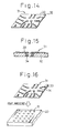
EXAMPLE 8
A thermoplastic polyimide adhesive of 35 µm thickness
("SPB" of Shin-Nittetsu Kagaku Kabushiki Kaisha) was
adhered to a polyimide film of 25 µm thickness with a
copper foil of 18 µm thickness ("Espanex" (Tradename) made
by Shin-Nittetsu Kagaku Kabushiki Kaisha). Then, a
plurlaity of holes each having 50 µm diameter were formed
at predetermined positions by an Excimer laser in such a
manner that said copper foil was exposed as respective
bottoms of the holes. Then, while the surface of the
copper foil was covered with a masking film, the holes
were filled with copper of 55 - 60 µm thickness by an
electric plating and subsequently filled with Sn-Pb solder
by an electric plating to form connecting vias. The
masking film was then removed and wiring patterns 31 of
line/space of 34 µm/34 µm having land portions of 110 µm
diameter for receiving the connecting vias were formed by
an etching process using liquid photoresist. Thus, as
shown in Figs. 14 and 15, a wiring pattern film or
substrate 31 comprising the polyimide film 32, wiring
patterns 33 and connecting vias 34 was obtained.
Thus obtained wiring pattern substrate 31 was then
laminated in a vacuum condition onto a core substrate 20
having a plurality of filled vias 18 which was the same as
that of the Example 1 as shown in Fig. 16 and unified
together with heat and pressure at a temperature of 190'C
under a pressure of 30kg/cm2 for 30 min. The both surfaces
of thus obtained laminated substrate were coated with
solder resist of photoresist and then plated with nickel
and gold. Then, the laminated substrate was cut into
individual packages, which were suitable for flip chip
type semiconductor devices.
As described above, according to the wiring substrate
of the present invention, it is possible to reduce the
manufacturing cost by using a common standardized core
substrate. Since the fine metallic wires are arranged in
the core substrate, the radiating property of the wiring
substrate can be enhanced.
When the filled vias, which are not connected with
the wiring pattern, are connected with the grounding
terminals, it is possible to reduce the occurrence of
cross talk, and the electrical characteristics can be
improved.