BACKGROUND OF THE INVENTION
The present invention relates to non-volatile
semiconductor memory device and, more particularly,
to an electrically erasable and programmable read only
memory device (EEPROM) including a plurality of memory
cell transistors each having a control gate and a floating
gate.
As well known in the art, each of cell transistors
employed in such an EEPROM is constructed such that
a floating gate is formed over a channel region of
a semiconductor substrate defined by source and drain
regions with an intervention of a gate insulating film,
and a control gate is formed on another gate insulating
film covering the floating gate. By applying a certain
voltage between the control gate and the drain region,
carriers such as electrons are injected and extracted
into and from the floating gate. The EEPROM of this type,
however, requires a relatively complicated manufacturing
process because of forming the control gate over the
floating gate.
Therefore, such an EEPROM is disclosed in Japanese
Patent Application Disclosure SHO No. 59-155968 that
simplifies the manufacturing process. This EEPROM
constitutes a control gate with a diffusion region.
Referring to Figs. 10(A) and 10(B), each memory cell
in such an EEPROM includes N+-type impurity diffusion
layers 23, 24, 25 and 26 selectively formed in a device
formation region or an active region on a P-type single-crystal
silicon substrate 21 which is partitioned or
defined by a field oxide layer 22. This memory cell
is composed of a cell transistor and a select transistor.
The diffusion layer 23 serves as a source region of the
cell transistor, and the diffusion layer 24 serves as a
drain region of the cell transistor and further as a
source region of the select transistor. The diffusion
layer 25 operates as a drain region of the select transistor.
This region 25 also serves as a bit line. The diffusion
layer 26 serves as a control gate of the cell transistor.
This region 26 is covered with a gate insulating film 28
made of silicon oxide, on which a floating gate 29 made
of polysilicon is formed. The floating gate 29 is elongated
over a gate insulating film 27 covering the channel region
between the source region 23 and the drain region 24.
The channel region between the regions 24 and 25
for the select transistor is covered with a gate insulating
film 30, over which a selector gate 31 for the select
transistor crosses. Each of the floating gate 29 and the
selector gate 31 may be formed simultaneously as a first
level wiring layer of a multi-level wiring structure.
A silicon oxide layer 32 is formed over the entire
surface by the so-called CVD method. Formed on the
silicon oxide layer 32 is horizontal direction in parallel
to each other are an aluminum common line 34 connected to
the source region 23 through a contact hole 33 and a bit
line 36 made of aluminum connected to the bit line region
25 through a contact hole 35.
Although only one memory cell is shown in Fig. 10,
a control gate region 26 is elongated to be employed in
common for the adjacent cells, as shown in Fig. 11.
Further, in order to reduce the resistance of the region
26, a wiring layer 37 is formed along the region 26 and
connected thereto via contact holes 38. It is to be
noted that, the wiring 37 is buried in the insulating
layer 32 and made of polysilicon. The wiring layer 37
is further formed to cover the floating gates 29 via the
silicon oxide layer 32.
Referring to Fig. 12, the memory cell thus constructed
has a cell transistor Qm and a select transistor Qc.
As is also apparent from the above description, the
transistors Qm and Qc are connected to the word line
WLi (31), the wiring line (CGi) 37, the common line
(CLj) 34 and the bit line (BLj) 36.
An erasing operation for the above cell is performed
by setting the drain region 24 to 0 volts and the control
gate region 26 to a higher potential, Electrons are
thereby injected into the floating gate 29 by the Fowler-Nordheim
(F-N) tunnel effect from the drain region 24.
Conversely, a programming operation for the cell is
performed by setting the control gate region 26 to 0 volts
and the drain region 24 to a higher potential. The
electrons are thus extracted from the floating gate 29
through the silicon oxide layer 27 by an F-N tunnel effect
to the drain region. Thus, the injection and extractions
of carriers are performed in this EEPROM, like the
conventional EEPROM.
Here, representing the voltage between the drain
region 24 and programming region 26 as VCG, the capacitance
(of the section of the silicon oxide layer 27) between
the floating gate 29 and the drain region 24 as C1, and
the capacitance (of the section of the silicon oxide
layer 28) between the floating gate 29 and the programming
region 26 as C2, the potential of the floating gate FG is
expressed as follows:
VFG = VCG · C2 / (C1 + C2)
As is apparent from the operation (1), the voltage
VFG may be increased by decreasing the capacitance C1,
i.e., the facing area of the floating gate 29 and the
drain region 24. The voltage needed for erasing and
programming can be reduced accordingly. In other words,
the EEPROM can operates on a reduced power voltage.
However, decreasing the facing area between the floating
gate 29 and the drain region 24 of the cell transistor
results in decrease in size of the cell transistor, so that
the on-state current of the cell transistor is reduced to
lower an operation speed.
A semiconductor memory device according to the preamble of
claim 1 is disclosed in FR-A-2562707.
A floting-gate MOSFET for an EEPROM is disclosed in IEEE
EDL-12, no. 3, EP 111-113.
It is an object of the invention to provide an EEPROM prom
having at least a memory cell of a structure that enhances
a voltage applied to a floating gate on erasing and programming
without lowering integration density.
It is an object of the invention to provide a semiconductor
memory device according to the preamble of
claim 1 in which supplying of a programming voltage to
the programming region is speeded up.
These objects are achieved by a semiconductor memory device
as defind in claim 1, i.e. according to the invention the
programming region is separated from each of source and
drain regions; the dependent claims are related to further
developments of the invention.
BRIEF DESCRIPTION OF THE DRAWINGS
The above and other objects, advantages and features
of the present invention will be more apparent from
the following description taken in conjunction with
the accompanying drawings, in which:
DETAILED DESCRIPTION OF THE PREFERRED EMBODIMENTS
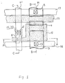
Referring now to Fig. 1 as well as Figs. 2(A), (B)
and (C), the description will be made on a memory cell
according to the first embodiment of the present invention.
This memory cell is formed on a monocrystalline silicon
substrate as a semiconductor substrate. This substrate
is of a P-type as one conductivity type. A plurality of
device formation regions or active regions are provided
and defined in the substrate 1 by a field oxide layer 2.
The memory cell illustrated therein is composed of
a cell transistor and select transistor. The cell
transistor has diffusion layers 3, 4 and 6 as a drain
region, a source region and a programming region,
respectively. The select transistor has diffusion
regions 4 and 5 as a drain region and a source region,
respectively. Each of the regions 3 - 4 is of an N-type
as the other conductivity type.
As is apparent from the drawings, a gate insulating
layer 7 made of silicon oxide is formed on a part of
the drain region 3, a channel region between the drain
region 3 and source region 4, and another gate insulating
film 8 made of silicon oxide is formed on a part of the
programming region 6. A floating gate 9 made of polysilicon
is formed on the gate insulating film 7 and 8
in such a shape as shown in the drawings. Since the
floating gate 9 overlaps with a major part of the drain
region 3, each of the regions 3 - 6 is formed by ion
implantation prior to the formation of the floating gate
(FG), unlike the conventional method.
There is further provided a selector gate 11 made
of polysilicon over a channel region between the source
region 4 and bit line region 5 with an intervention of
a gate oxide layer 10. The floating gate 9 and the
selector gate 11 may be formed simultaneously as a first
level of wiring layer.
An interlayer insulating layer 12 is formed over
the entire surface, and contact holes 13, 14 and 15 are
made therein. An aluminum common line 16 is formed to be
connected to the region 3 through the contact hole 13,
an aluminum bit line 17 is formed to be connected to the
region 5 through the contact hole 14. A contact metal 18
made of aluminum is formed to fill the contact hole 15 to
be connected to the programming region 6. These metal
lines 16, 17 and 18 are formed as a first level metal
wiring layer.
A second inter-layer insulating layer 19 is formed
over the entire surface, through which a through-hole 20
is formed, and a wiring line 21 made of aluminum is formed
to be connected to the contact metal 18 and thus to the
programming region 6.
As is apparent from Fig. 1 and further from Fig. 3,
the facing area between the floating gate 9 and the part
of the drain region 3 is made larger than the facing area
between the floating gate 9 and the programming region 6.
Accordingly, representing the voltage applied across the
drain region 3 as VD, the capacitance between the floating
gate 9 and the part of drain region 3 as C1, and the
capacitance between the floating gate 9 and programming
region 6 as C2, the potential of the floating gate FG is
expressed as follows:
VFG = VD ·C1 / (C1 + C2)
Here, if the silicon oxide layers 7 and 8 have an
identical thickness, then
VFG = VD ·S1 / (S1 + S2)
wherein S1 is the overlapping area between the
floating gate 9 and the drain region 3, and S2 is the
overlapping area between the floating gate and the
programming region 6. Since the area S2 is made
considerably small as compared with the area S1, the
F-N tunnel phenomenon takes place mainly at the silicon
oxide layer 8 covering the programming region 6. That
is,the injection and extraction of carriers into and from
the floating gate 9 occur at the programming region 6 in
place of the drain region 3.
In the present embodiment, the capacitance ratio of
C1 : C2 is designed to be 10 : 1, so that 90% of the
applied voltage may be effectively utilized as the
floating gate voltage VFG. Taking into account the
fluctuations depending on the respective processes,
however, it is preferrable to set the radio of C1 : C2
to be 20 : 1 or more.
As mentioned above, according to the present
invention, electrons are designed to be injected and
extracted (or ejected) between the floating gate 19 and
the programmable region 6.
Referring to Fig. 4, the memory cell thus constructed
is composed of the memory transistor Qm and the select
transistor Qs which are connected to programming line 21,
the common line (CLj) 16, the bit line (BLj) 17 and the
word line (WLi) 11.
An erasing operation for each cell Cij is performed
by setting the controllable region 6 to 0 volts, the
drain region 3 to a high potential and the source region 4
open. The electrons are thus injected into the floating
gate 9 via the silicon oxide layer 8 by the F-N tunnel
effect from the programming region 6.
A programming operation for each cell Cij is performed
by setting each of the drain region 3 and source region 4
to 0 volt and the programming region 6 to the high
potential. The electrons are thereby extracted or
released from the floating gate 29 by the F-N tunnel
effect to the programming region 6. The erased state
is an enhancement state and the written state is a
depletion state, and thus the binary determination is
performed depending on whether electrons are included
or not. The memory may be used in the opposite state
depending on its manner of use. It is therefore in a
reading operation the line 22 (the programming region 6)
is supplied with a reading voltage of 0 volt while turning
the select transistor Qs conductive by selecting the word
line 11. If desired, the reading voltage may be negative
or positive.
On the other hand, in cases where a particular cell
Cij is not selected, all that is needed is to set the
potential of the programmable region 6 or drain region 3
(common bit line CLj) to about half the level when
selected. With this reduction, the non-selected cell
fails to undergo a sufficient potential difference to
generate an F-N tunnel current, and thus neither writing
nor erasing is accomplished.
Reading operation is performed by setting the word
line (selector gate) WLi to a high level of potential to
read out data in the bit line BLj. This setting allows
exclusion of influence of a large junction capacitance of
the drain region 3 with a great area. More specifically,
in cases where a large junction capacitance is present
at the reading end, the capacitance functions as the
capacitance at the drain end o fthe transistor to lower
the charging and discharging efficiency of the transistor,
and consequently the reading speed is slowed.
In addition, as show in Fig. 13, since a plurality of
cells are connected to a single polysilicon-made control
gate line 37 according to the prior art in order to prevent
delays in application of a voltage to the control gate
region 26, the effect of preventing delays in application
of a voltage is accomplished on a plurality of cells as
a group, and thus the prior art fails to overcome delays
in application of a voltage which is caused by the control
gate region 26 itself.
In contrast, however, according to the first
embodiment of the present invention, the programming
region 6 is independent and isolated per cell, and each
programming region is individually connected to a metal
layer 18 and a wiring line 21. As a result, the
programming region 6 itself does not cause delays in
application of a voltage.
Here, the programming region 6 may be extended in
the same manner as the aluminum-made control gate line
shown in Fig. 1. The region is not shown in such an
extended manner in the present embodiment only for space
considerations.
Fig. 5 shows an instance of writing or erasion
operation for the aforementioned cell construction.
In cases where the silicon oxide films 7 and 8 are
approximately 9.0 nm thick, application of a pulse of
12 volts for 1 ms produces 100 uA or more of writing-on
resistor current ION and 0.1 nA or less of erasion-off
current IOFF, and operation may be performed at 12 volts.
This proves that the present invention allows lowering
in the voltage, that is, improvement in the efficiency
of the F-N tunnel effect as compared with the prior art
which requires as a high potential as approximately
20 volts.
Fig. 6 is a cross sectional view which shows a
second embodiment of the non-volatile IC memory according
to the present invention, which drawing is a counterpart
of Fig. 2(B). Concretely, oxidation-resistant insulator
layers (sidewall layers) 42 are formed on the respective
sidewalls of the floating gate 9 and selector gate 11 to
protect the floating gate 9. More specifically, this
protection serves to prevent acceleration of oxidation
of the silicon oxide layer 7 beneath the floating gate 9
in the later steps and to prevent oxidation of the floating
gate 9 and silicon substrate 1. As a result, the writing
and erasion operation properties may be protected from
being impaired. Here, the oxidation-resistant insulator
layers 42 may be formed by etching back after the floating
gate 9 and selector gate 11 have been oxidized.
Fig. 7 is a cross sectional view which shows a third
embodiment of the non-volatile IC memory according to
the present invention, which drawing is a counterpart
of Fig. 2(B). Concretely, instead of the layer 10, a
thicker gate oxide layer 10' is provided beneath the
selector gate 11 to improve the resistance of the
selector transistor to the insulator layer and thus to
increase its reliability.
Fig. 8 is a plan view which shows a fourth embodiment
of the non-volatile IC memory according to the present
invention, and Fig. 9 is a cross sectional view taken
on line IX-IX in Fig. 8. Referring to Fig. 8 and Fig. 9,
a polysilicon protecting gate 44 is further provided on
the floating gate 9 with an intervention of an insulating
layer (e.g., silicon oxide layer) 43. The drain region 3
in this embodiment is formed to have a projecting portion
to which the protecting gate 44 is connected to through
a contact hole 45. Since the additional gate 44 is
provided, there exists the parallel connection of the
capacitance C3 between the floating gate 9 and protecting
gate 44 and the capacitance C1 between the floating gate 9
and drain region 3, so that the following equation is
derived:
VFG = VD (C1 + C3) / (C1 + C2 + C3)
The VFG is thus increased. In other words, the same
value of VFG may be obtained with a smaller capacitance C1,
that is, with a smaller area of the facing sections of the
floating gate 9 and drain region 3, which contributes to
high degrees of integration. As an example, assuming that
the thickness of the silicon oxide layer 7 is 90 Å, the
thickness of the insulator layer 43 is 180 Å, the area of
the facing sections of the floating gate 9 and protecting
gate 44 is ΔS, the same value of VFG may be obtained with
a reduction ΔS' of the area of the facing sections of the
floating gate 9 and drain region 3, which may be calculated
as follows:
εS1/90 Å = ε(S1 - ΔS') / 90 Å + εΔS / 180 Å
∴ ΔS' = ΔS/2
wherein ε is the dielectric constant of the oxide
layer. High degrees of integration may be accomplished
in this way.
As explained above, according to the present
invention, since no F-N tunnel effect is produced
between the floating gate and drain region, electrons
are not trapped in the insulator layer for the cell
transistor, and thus the properties of the cell transistor
are protected from being impaired. In addition, the
voltage VFG across the floating gate may be increased
to enhance the F-N tunnel effect.
Further, since a separate programmable region is
provided for each cell, delays in application of a voltage
may be prevented. Furthermore, reading operation may be
accelerated since the reading operation is performed from
the source drain end with a small junction capacitance.
Moreover, since the programmable region is not
designed to function as a transistor, the area of the
facing sections of the floating gate and programmable
region may be minimized to limits, and the area of the
,facing sections of the floating gate and drain region
may be determined correspondingly, and thus the voltage
VFG across the floating gate may be increased accordingly
to enhance the F-N tunnel effect.
In addition, since the programmable region is
provided independently for each cell, delays in feeding
a voltage are negligible.
It is apparent that the presnet invention is not
limited to the above embodiments but may be modified
and changed without departing from the scope and spirit
of the invention.