EP0880196A1 - Compact monopulse source for an antenna with optical focusing - Google Patents
Compact monopulse source for an antenna with optical focusing Download PDFInfo
- Publication number
- EP0880196A1 EP0880196A1 EP98401179A EP98401179A EP0880196A1 EP 0880196 A1 EP0880196 A1 EP 0880196A1 EP 98401179 A EP98401179 A EP 98401179A EP 98401179 A EP98401179 A EP 98401179A EP 0880196 A1 EP0880196 A1 EP 0880196A1
- Authority
- EP
- European Patent Office
- Prior art keywords
- source according
- waveguides
- source
- transmission
- previous
- Prior art date
- Legal status (The legal status is an assumption and is not a legal conclusion. Google has not performed a legal analysis and makes no representation as to the accuracy of the status listed.)
- Granted
Links
Images


Classifications
-
- H—ELECTRICITY
- H01—ELECTRIC ELEMENTS
- H01Q—ANTENNAS, i.e. RADIO AERIALS
- H01Q25/00—Antennas or antenna systems providing at least two radiating patterns
- H01Q25/02—Antennas or antenna systems providing at least two radiating patterns providing sum and difference patterns
-
- H—ELECTRICITY
- H01—ELECTRIC ELEMENTS
- H01Q—ANTENNAS, i.e. RADIO AERIALS
- H01Q19/00—Combinations of primary active antenna elements and units with secondary devices, e.g. with quasi-optical devices, for giving the antenna a desired directional characteristic
- H01Q19/10—Combinations of primary active antenna elements and units with secondary devices, e.g. with quasi-optical devices, for giving the antenna a desired directional characteristic using reflecting surfaces
- H01Q19/12—Combinations of primary active antenna elements and units with secondary devices, e.g. with quasi-optical devices, for giving the antenna a desired directional characteristic using reflecting surfaces wherein the surfaces are concave
- H01Q19/17—Combinations of primary active antenna elements and units with secondary devices, e.g. with quasi-optical devices, for giving the antenna a desired directional characteristic using reflecting surfaces wherein the surfaces are concave the primary radiating source comprising two or more radiating elements
Definitions
- the present invention relates to a primary source with at least two-way, so-called monopulse, compact for an optical antenna focusing, for example of the Cassegrain or lens type, connected to a circuit microwave transmission and reception carried out for example in microstrip technology. It applies in particular to speed cameras millimeters fitted to motor vehicles. More generally, it applies to millimeter radars requiring a high level of integration and a low cost of realization.
- a so-called monopulse source for example has two channels and generates two radiation patterns simultaneously, one diagram sum and a difference diagram.
- This source must present compatible radio characteristics of adaptation performance and radiation from a complete focusing antenna. These characteristics especially the adaptation frequency band, the formation of diagram of the path difference in the plane of the electric field E and the openings and the relative level of the radiation patterns of the channels sum and difference.
- a solution to achieve a primary source satisfying some previous criteria is to use an excited pyramid horn by a magic tee folded in the plane of the electric field E. According to the access used, this magic tee allows to generate in the horn the transverse mode electric TE01, even mode, or transverse magnetic mode TM11, mode odd, respectively forming the sum and difference diagrams.
- this solution presents a congestion in depth important and requires, for its realization, the manufacture and assembly of several pieces of high precision leading to the use of methods expensive machining such as wire EDM or electro-forming.
- Another solution is to produce a printed source on the same substrate as the microwave transmission circuit.
- this source must consist of a network of radiating elements of the type ⁇ patch ⁇ powered for example by a hybrid ring.
- This solution has the advantage of not requiring any mechanical parts and have a minimum size at depth but does not meet the electromagnetic shielding and protection requirements environmental constraints for the components of the transmission circuit and microwave reception.
- the radiating elements of the type ⁇ patch ⁇ have a selective frequency operation and are therefore very sensitive to the characteristics of the substrate such as in particular its dielectric constant or its thickness, as well as etching tolerances.
- the object of the invention is to overcome the aforementioned drawbacks and to allow in particular to produce a source meeting the criteria set out previously.
- the invention relates to a monopulse source for antenna with focusing optics, characterized in that it comprises minus two waveguides machined in the metal sole supporting the antenna microwave transmission and reception circuit
- the main advantages of the invention are that it also applies both to a folded optics antenna and to a direct optics antenna, that it allows access from the source by a microstrip line, that it allows to modify the directivity of the radiation diagrams in the plane magnetic H and in the electric plane E, that it allows weak leaks radioelectric, that it allows to have the active components of the circuit transmission and reception near the source, that it is simple to implement and that it is economical.
- Figure 1a shows an example of an antenna with folded optics powered by a primary source 1 called monopulse, that is to say a source with two channels, a sum channel ⁇ and a difference channel ⁇ .
- the antenna comprises in particular a main reflector 2, for example of the type parabolic, and a sub-reflector 3.
- the primary source 1 is arranged behind the main reflector 2 and radiates through a hole 4 made in this last.
- the sub-reflector 3 is arranged opposite the source primary 1.
- the rays 5 emitted from the primary source 1 are reflected on the sub-reflector 3 then on the main reflector 2. After reflection on the latter, the rays 5 'are emitted in parallel at the antenna outlet.
- the invention applies to an antenna with folded optics, but it can also be applied for example for a direct optical antenna as shown in Figure 1b.
- This last comprises for example a dielectric lens 11 which focuses the rays 5 emitted by the source 4 at infinity.
- FIG 2 shows an exemplary embodiment according to art prior.
- Primary source 1 uses a rectangular waveguide 26 extended by a pyramid cone 27.
- the sum and difference paths of a tee magic 28 are fed via microstrip guide transitions 21, 22.
- the transmission and reception circuits 23, in technology microstrip, are implanted on a dielectric substrate 24, itself for example arranged on a metal sole 25.
- the waveguide is excited by the magic tee 28 folded in the plane of the electric field E. According to the access used, this magic tee allows to generate in the cornet the transverse electric mode TE10, even mode, or transverse mode magnetic TM11, odd mode, respectively forming the diagrams of sum and difference radiation.
- Access to the difference path from the tee magic can be obtained, via an elbow made in the plane of the field electric E, in the same plane as the access to the sum track.
- This source can then be connected to the transmission and reception circuit 23 by via two microstrip-guide transitions 21, 22.
- This solution unfortunately has a significant bulk in depth, the order for example of 35 mm in millimeter strip, and requires, as indicated above, the manufacture and assembly of several pieces of high precision, such as a magic tee 28 and transitions microstrip-guide 21, 22, which leads to the use of machining methods expensive. These methods are for example wire EDM or electro-forming.
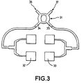
- FIG. 3 shows another known example of embodiment.
- the source is printed on the same substrate as the transmission circuit and reception. It includes in particular a balanced hybrid ring 31 of the type 4 ⁇ / 4 and a network of two pairs of elements or ⁇ patches ⁇ radiant 32, 33.
- the ring 31 feeds the radiating elements by two outputs 34, 35 one of which is extended by a quarter wavelength ⁇ / 4 relative to each other so as to feed in phase or in opposition to phase the two pairs of radiating elements 32, 33 following the entry 36, 37 of the ring which is excited.
- the radiation pattern of the sum channel is thus formed when the two pairs are excited in phase and the radiation pattern of the difference pathway is thus formed when the two pairs are excited in phase opposition.
- this exemplary embodiment has the advantage of not require no mechanical parts and present a space requirement minimal in depth but does not meet shielding requirements electromagnetic and protection against environmental constraints for the components of the microwave transmission and reception circuit.
- the radiating ⁇ patches 32 32, 33 have an operation frequency selective and are therefore very sensitive to the characteristics of the substrate such as in particular its dielectric constant or its thickness as well as engraving tolerances.
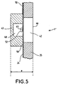
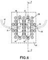
- FIGS 4, 5 and 6 show an exemplary embodiment possible from a primary source according to the invention.
- This source has two radiating waveguides 41, 42 machined in the metal sole 25 supporting the microwave transmission and reception circuit of the antenna, this circuit being for example in microstrip and / or MMIC technology according to the Anglo-Saxon expression ⁇ Monolithic Microwave Integrated Circuit ⁇ .
- the transmission and reception circuit is for example arranged on a substrate dielectric 24, itself mounted on the metal sole 25.
- the lines microstrip are for example screen printed or engraved on the substrate.
- the long side of the waveguides 41, 42 is for example dimensioned for allow the propagation of the transverse electric mode TE01 and to obtain in the magnetic plane H, the desired directivity of the radiated diagram on track.
- the distance between the two waveguides 41, 42 is by example determined to obtain in the plane of the electric field E, the desired directivity of the radiated diagram in sum channel.
- each waveguide is for example excited by a transition 44, 45 with the transmission circuit and reception, for example in microstrip technology, the transition being constituted for example by an engraved pattern 44, 45 on the same substrate as the one supporting the microstrip circuit, and by a short circuit microwave 43 closing the waveguide.
- the significant mismatch of the radiating mouth 46 of each guide 41, 42 is advantageously compensated by a change of section placed at a given distance of this mouth, each waveguide extending into a waveguide reduces 47, 48 from this section change.
- Section reduction is for example performed on the long side of the guide, in a factor of two for example.
- Each transition 44, 45 with the microstrip circuit is positioned in the section change plane.
- a transition 44, 45 is adapted by microwave short circuit 43 closing the waveguide reduced 47, 48 and placed at a distance substantially equal to a quarter of the wavelength ⁇ / 4 of the signal transmitted by the microstrip circuit.
- Each transition 44, 45 is for example supplied by a microstrip line 49, 50 passing under a tunnel 51, 52 made in the wall of the reduced waveguide.
- Each transition 44, 45 is then for example connected to a hybrid ring 53 balanced type 4 ⁇ / 4 with one of the outputs 55 extended by a quarter of wavelength ⁇ / 4 relative to the other 54.
- These links 49, 54, 50, 55 allow the two to be supplied in phase or in phase opposition radiating elements following the entry 56, 57 of the ring 53 which is excited and thus make it possible to form the diagrams of the sum and difference channels, the difference diagram being for example obtained in the plane of the field electric E.
- the two inputs 56, 57 of the hybrid ring are connected to the rest of the transmission and reception circuit 23.
- Each radiating element aforementioned consists in fact of a mouth 46 of waveguide and a transition 44, 45 with the microstrip circuit. Active components of the circuit transmission and reception can be placed near the source, this which allows in particular to limit microwave losses.
- the protection of the transmission and reception circuit microwave against parasitic electromagnetic radiation outside and located outside the radar operating band is ensured by the presence of waveguides which play the role of high-pass filter.
- the section of the waveguides 41, 42, 47, 48 is for example oblong instead of being rectangular, this notably avoids the use of expensive machining methods such as wire EDM.
- the oblong sections can be simply made by a means economical machining such as milling.
- the architecture of a source according to the invention allows it to present a wide band busy, thanks in particular to the use of an excitation element not selective, which makes parts manufacturing tolerances less sensitive mechanical and microstrip circuits, and therefore further contributes to reducing manufacturing costs.
- the short circuit 43 for adapting the transitions 44, 45 and the guides of reduced section 47, 48 can be machined in the same part. That allows in particular to reduce the number of parts to be machined.
- This piece can be assembled and positioned relative to the metal sole 25, and therefore in particular with respect to the microstrip circuit and the waveguides 41, 42 by any method, such as for example screwing, brazing or collage.
- this part 43, 47, 48 can be electrically connected by at least one point, but preferably by several, to the metal sole 25 supporting the circuit in technology microstrip.
- metallized holes can be made in the dielectric substrate for example on the periphery of the guides 41, 42 machined in the metal sole 25.
- the metal sole 25 in which the radiating guides 41, 42 are made can for example be an integral part of the housing containing the transmission and reception circuit, which makes the realization even more compact and also reduces the number of workpieces.
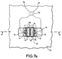
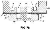
- Figures 7a and 7b show a possible embodiment a primary source according to the invention making it possible to obtain a diagram particular radiation of the sum and / or difference channels of the source, for example to obtain a better adaptation to the characteristics of focusing optics.
- false slots 71, 72 are added to the in the vicinity of the waveguides 41, 42 machined in the metal sole 25. These false slots 71, 72 are holes which do not completely cross the sole 25. These false slots, which for example have the same section transverse as the waveguides, are actually traps that are excited by coupling thanks to the proximity of the waveguides. The energy captured by coupling with these waveguides 41, 42 is radiated.
- a surface 73 is by example made, by counterbore, inside the sole 25.
- This surface 73, as well as the false slots 71, 72 are for example obtained during of the same machining operation as the waveguides 41, 42 of the sole metallic 25.
- the decrease in the thickness of the sole 25 begins substantially at right 74 of the waveguides 41, 42 and of the false slots 71, 72.
- FIGS 4, 5, 6 and 7 describe an exemplary embodiment of a two-channel monopulse primary source.
- the invention can nevertheless be applied for three-way sources, for example with a sum channel and a path difference in the plane of the electric field E and a path difference in the plane of the magnetic field H.
- This source is then by example obtained by associating four radiating elements supplied by four hybrid rings, each radiating element being for example consisting of a waveguide mouth 46 and a transition with the microstrip circuit as described above.
- the invention can also be applied for the production from a primary source illuminating a multi-beam antenna.
- This source is for example formed by several radiating elements, such as those mentioned above, placed in the focal plane of a type reflector system Cassegrain or in the focal plane of a dielectric lens, each element radiating generating a beam whose inclination depends on the position of the elementary source compared to the hearth.
- the invention allows very good protection circuits against environmental constraints, such as for example moisture or corrosion, partially or completely filling the guides radiating with dielectric material.
- environmental constraints such as for example moisture or corrosion
- Such protection is particularly advantageous for radars fitted to automobiles and which are liable to undergo the above-mentioned constraints.
- a source produced according to the invention occupies a small footprint e in depth, this may for example be of the order of 5 mm in millimeter band, this footprint going from the outer end of the microwave short-circuit 43 to the output 46 of a waveguide 41, 42.
Abstract
Description
La présente invention concerne une source primaire à au moins deux voies, dite monopulse, compacte pour une antenne à optique focalisante, par exemple de type Cassegrain ou à lentille, reliée à un circuit d'émission et de réception hyperfréquence réalisé par exemple en technologie à microruban. Elle s'applique notamment aux radars millimétriques équipant des véhicules automobiles. Plus généralement, elle s'applique à des radars millimétriques nécessitant un haut niveau d'intégration et un faible coût de réalisation.The present invention relates to a primary source with at least two-way, so-called monopulse, compact for an optical antenna focusing, for example of the Cassegrain or lens type, connected to a circuit microwave transmission and reception carried out for example in microstrip technology. It applies in particular to speed cameras millimeters fitted to motor vehicles. More generally, it applies to millimeter radars requiring a high level of integration and a low cost of realization.
Une source dite monopulse présente par exemple deux voies et génère simultanément deux diagrammes de rayonnement, un diagramme somme et un diagramme différence. Cette source doit présenter des caractéristiques radioélectriques compatibles des performances d'adaptation et de rayonnement d'une antenne focalisante complète. Ces caractéristiques concement notamment la bande de fréquence d'adaptation, la formation du diagramme de la voie différence dans le plan du champ électrique E et les ouvertures et le niveau relatif des diagrammes de rayonnement des voies somme et différence.A so-called monopulse source for example has two channels and generates two radiation patterns simultaneously, one diagram sum and a difference diagram. This source must present compatible radio characteristics of adaptation performance and radiation from a complete focusing antenna. These characteristics especially the adaptation frequency band, the formation of diagram of the path difference in the plane of the electric field E and the openings and the relative level of the radiation patterns of the channels sum and difference.
Dans certaines applications, telles qu'une application à des véhicules automobiles par exemple, la source doit en outre répondre notamment à des critères techniques, technologiques et économiques d'ordre général et aussi particuliers. Ces critères sont par exemple les suivant :
- facilité de connexion et d'implantation au plus près du circuit d'émission et de réception hyperfréquence, ce dernier étant réalisé en technologie en micro-ruban, dite microstrip, de manière à minimiser les longueurs de lignes dont les pertes importantes dans la bande millimétrique, de l'ordre par exemple de 80 dB, peuvent limiter rapidement les performances du système ;
- blindage du circuit d'émission et de réception hyperfréquence vis-à-vis des contraintes électromagnétiques externes en dehors de la bande de fonctionnement du système ;
- faible encombrement en profondeur de la source primaire, par exemple inférieur à 5 mm ;
- étanchéité et éventuellement herméticité du circuit d'émission et de réception vis-à-vis des contraintes d'environnement extérieures, l'ensemble constitué du circuit d'émission et de réception et de la source primaire pouvant constituer un macro-composant ;
- réalisation par des moyens de fabrication classiques et présentation d'un fonctionnement tolérant vis-à-vis des dispersions dimensionnelles obtenues avec ces moyens de fabrication dans le cadre d'une production de masse à très faible coût.
- ease of connection and installation as close as possible to the microwave transmission and reception circuit, the latter being produced using micro-ribbon technology, known as microstrip, so as to minimize line lengths, including significant losses in the millimeter band , for example of the order of 80 dB, can quickly limit the performance of the system;
- shielding of the microwave transmission and reception circuit against external electromagnetic constraints outside the operating band of the system;
- small overall depth of the primary source, for example less than 5 mm;
- sealing and possibly hermeticity of the transmission and reception circuit with respect to external environmental constraints, the assembly consisting of the transmission and reception circuit and of the primary source being able to constitute a macro-component;
- realization by conventional manufacturing means and presentation of an operation tolerant with respect to the dimensional dispersions obtained with these manufacturing means in the context of mass production at very low cost.
Une solution pour réaliser une source primaire satisfaisant à certains critères précédents, consiste à utiliser un cornet pyramidal excité par un té magique replié dans le plan du champ électrique E. Suivant l'accès utilisé, ce té magique permet de générer dans le cornet le mode transverse électrique TE01, mode pair, ou le mode transverse magnétique TM11, mode impair, formant respectivement les diagrammes somme et différence. Cependant cette solution présente un encombrement en profondeur important et nécessite, pour sa réalisation, la fabrication et l'assemblage de plusieurs pièces de grande précision conduisant à l'emploi de méthodes d'usinage onéreuses telles que l'électro-érosion à fils ou l'électro-formage.A solution to achieve a primary source satisfying some previous criteria, is to use an excited pyramid horn by a magic tee folded in the plane of the electric field E. According to the access used, this magic tee allows to generate in the horn the transverse mode electric TE01, even mode, or transverse magnetic mode TM11, mode odd, respectively forming the sum and difference diagrams. However this solution presents a congestion in depth important and requires, for its realization, the manufacture and assembly of several pieces of high precision leading to the use of methods expensive machining such as wire EDM or electro-forming.
Une autre solution consiste à réaliser une source imprimée sur le même substrat que le circuit d'émission hyperfréquence. Pour former les diagrammes de rayonnement présentant la directivité souhaitée, cette source doit être constituée d'un réseau d'éléments rayonnants de type 〈〈 patch 〉〉 alimentés par exemple par un anneau hybride. Cette solution présente l'avantage de ne nécessiter aucune pièce mécanique et de présenter un encombrement minimal en profondeur mais ne répond pas aux exigences de blindage électromagnétique et de protection vis-à-vis des contraintes d'environnement pour les composants du circuit d'émission et de réception hyperfréquence. Par ailleurs, les éléments rayonnants de type 〈〈 patch 〉〉 présentent un fonctionnement sélectif en fréquence et sont donc très sensibles aux caractéristiques du substrat telles que notamment sa constante diélectrique ou son épaisseur, ainsi qu'aux tolérances de gravure. Another solution is to produce a printed source on the same substrate as the microwave transmission circuit. To train radiation patterns with the desired directivity, this source must consist of a network of radiating elements of the type 〈〈 patch 〉〉 powered for example by a hybrid ring. This solution has the advantage of not requiring any mechanical parts and have a minimum size at depth but does not meet the electromagnetic shielding and protection requirements environmental constraints for the components of the transmission circuit and microwave reception. Furthermore, the radiating elements of the type 〈〈 patch 〉〉 have a selective frequency operation and are therefore very sensitive to the characteristics of the substrate such as in particular its dielectric constant or its thickness, as well as etching tolerances.
Le but de l'invention est de pallier les inconvénients précités et de permettre notamment de réaliser une source répondant aux critères exposés précédemment. A cet effet, l'invention a pour objet une source monopulse pour antenne à optique focalisante, caractérisée en ce qu'elle comporte au moins deux guides d'onde usinés dans la semelle métallique supportant le circuit d'émission et des réception hyperfréquence de l'antenneThe object of the invention is to overcome the aforementioned drawbacks and to allow in particular to produce a source meeting the criteria set out previously. To this end, the invention relates to a monopulse source for antenna with focusing optics, characterized in that it comprises minus two waveguides machined in the metal sole supporting the antenna microwave transmission and reception circuit
L'invention a pour principaux avantages qu'elle s'applique aussi bien à une antenne à optique repliée qu'à une antenne à optique directe, qu'elle permet un accès de la source par une ligne microstrip, qu'elle permet de modifier la directivité des diagrammes de rayonnement dans le plan magnétique H et dans le plan électrique E, qu'elle permet de faibles fuites radioélectriques, qu'elle permet de disposer les composants actifs du circuit d'émission et de réception à proximité de la source, qu'elle est simple à mettre en oeuvre et qu'elle est économique.The main advantages of the invention are that it also applies both to a folded optics antenna and to a direct optics antenna, that it allows access from the source by a microstrip line, that it allows to modify the directivity of the radiation diagrams in the plane magnetic H and in the electric plane E, that it allows weak leaks radioelectric, that it allows to have the active components of the circuit transmission and reception near the source, that it is simple to implement and that it is economical.
D'autres caractéristiques et avantages de l'invention apparaítront à l'aide de la description qui suit faite en regard de dessins annexés qui représentent :
- la figure 1a, un exemple d'antenne à optique repliée alimentée par une source primaire monopulse ;
- la figure 1b, un exemple d'antenne à optique directe alimentée par une source primaire monopulse ;
- la figure 2, un exemple de réalisation selon l'art antérieur d'une source primaire ;
- la figures 3, un autre exemple selon l'art antérieur d'une source primaire ;
- la figure 4, un mode de réalisation possible d'un exemple de source selon l'invention, par une vue de face suivant F', en regard de la semelle métallique ;
- la figure 5, une vue en coupe suivant F de la figure 4 ;
- la figure 6, un détail de la figure 4 au niveau des éléments rayonnant ;
- les figures 7a et 7b, un mode de réalisation possible de source selon l'invention où l'usinage de la semelle métallique modifie le diagramme de rayonnement, la figure 7b étant une vue en coupe de la figure 7a selon AA..
- FIG. 1a, an example of an antenna with folded optics supplied by a primary monopulse source;
- Figure 1b, an example of direct optical antenna powered by a primary monopulse source;
- Figure 2, an embodiment according to the prior art of a primary source;
- Figures 3, another example according to the prior art of a primary source;
- FIG. 4, a possible embodiment of an example of a source according to the invention, by a front view along F ', opposite the metal sole;
- Figure 5, a sectional view along F of Figure 4;
- Figure 6, a detail of Figure 4 at the radiating elements;
- FIGS. 7a and 7b, a possible embodiment of a source according to the invention where the machining of the metal sole changes the radiation diagram, FIG. 7b being a sectional view of FIG. 7a along AA.
La figure 1a présente un exemple d'antenne à optique repliée
alimentée par une source primaire 1 dite monopulse, c'est-à-dire une source
à deux voies, une voie somme Σ et une voie différence Δ. L'antenne
comporte notamment un réflecteur principal 2, par exemple de type
parabolique, et un sous-réflecteur 3. La source primaire 1 est disposée
derrière le réflecteur principal 2 et rayonne à travers un trou 4 réalisé dans
ce dernier. Le sous-réflecteur 3 est disposé en regard de la source
primaire 1. Les rayons 5 émis depuis la source primaire 1 se réfléchissent
sur le sous-réflecteur 3 puis sur le réflecteur principal 2. Après réflexion sur
ce dernier, les rayons 5' sont émis parallèlement en sortie d'antenne.Figure 1a shows an example of an antenna with folded optics
powered by a
L'invention s'applique pour une antenne à optique repliée, mais
elle peut aussi s'appliquer par exemple pour une antenne à optique directe
telle qu'illustrée par la figure 1b. Cette demière comporte par exemple une
lentille diélectrique 11 qui focalise à l'infini les rayons 5 émis par la source 4.The invention applies to an antenna with folded optics, but
it can also be applied for example for a direct optical antenna
as shown in Figure 1b. This last comprises for example a
La figure 2 présente un exemple de réalisation selon l'art
antérieur. La source primaire 1 utilise un guide d'onde rectangulaire 26
prolongé par un cornet pyramidal 27. Les voies somme et différence d'un té
magique 28 sont alimentées par l'intermédiaire de transitions guide-microstrip
21, 22. Les circuits d'émission et de réception 23, en technologie
microstrip, sont quant à eux implantés sur un substrat diélectrique 24, lui-même
par exemple disposé sur une semelle métallique 25. Le guide d'onde
est excité par le té magique 28 replié dans le plan du champ électrique E.
Suivant l'accès utilisé, ce té magique permet de générer dans le cornet le
mode transverse électrique TE10, mode pair, ou le mode transverse
magnétique TM11, mode impair, formant respectivement les diagrammes de
rayonnement somme et différence. L'accès de la voie différence du té
magique peut être obtenu, via un coude réalisé dans le plan du champ
électrique E, dans le même plan que l'accès de la voie somme. Cette source
peut alors être connectée au circuit d'émission et de réception 23 par
l'intermédiaire de deux transitions microstrip-guide 21, 22. Cette solution
présente malheureusement un encombrement important en profondeur, de
l'ordre par exemple de 35 mm en bande millimétrique, et nécessite, comme
indiqué précédemment, la fabrication et l'assemblage de plusieurs pièces de
grande précision, telles que par exemple un té magique 28 et les transitions
microstrip-guide 21, 22, ce qui conduit à l'emploi de méthodes d'usinage
onéreuses. Ces méthodes sont par exemple l'électro-érosion à fils ou
l'électro-formage.Figure 2 shows an exemplary embodiment according to art
prior.
La figure 3 présente un autre exemple connu de réalisation. La
source est imprimée sur le même substrat que le circuit d'émission et de
réception. Elle comporte notamment un anneau hybride 31 équilibré de type
4λ/4 et un réseau de deux paires d'éléments ou 〈〈 patches 〉〉
rayonnants 32, 33. Pour former les diagrammes de rayonnement présentant
la directivité souhaitée, l'anneau 31 alimente les éléments rayonnants par
deux sorties 34, 35 dont l'une est allongée d'un quart de longueur d'onde λ/4
par rapport à l'autre de manière à alimenter en phase ou en opposition de
phase les deux paires d'éléments rayonnant 32, 33 suivant l'entrée 36, 37 de
l'anneau qui est excitée. Le diagramme de rayonnement de la voie somme
est ainsi formé lorsque les deux paires sont excitées en phase et le
diagramme de rayonnement de la voie différence est ainsi formé lorsque les
deux paires sont excitées en opposition de phase. Comme il a été indiqué
précédemment, cet exemple de réalisation présente l'avantage de ne
nécessiter aucune pièce mécanique et de présenter un encombrement
minimal en profondeur mais il ne répond pas aux exigences de blindage
électromagnétique et de protection vis-à-vis des contraintes d'environnement
pour les composants du circuit d'émission et de réception hyperfréquence.
Par ailleurs, les 〈〈 patches 〉〉 rayonnant 32, 33 présentent un fonctionnement
sélectif en fréquence et sont donc très sensibles aux caractéristiques du
substrat telles que notamment sa constante diélectrique ou son épaisseur
ainsi qu'aux tolérances de gravure.FIG. 3 shows another known example of embodiment. The
source is printed on the same substrate as the transmission circuit and
reception. It includes in particular a
Les figures 4, 5 et 6 présentent un exemple de réalisation
possible d'une source primaire selon l'invention. Cette source comporte deux
guides d'onde rayonnant 41, 42 usinés dans la semelle métallique 25
supportant le circuit d'émission et de réception hyperfréquence de l'antenne,
ce circuit étant par exemple en technologie microstrip et/ou MMIC selon
l'expression anglo-saxonne 〈〈 Monolithic Microwave Integrated Circuit 〉〉. Le
circuit d'émission et de réception est par exemple disposé sur un substrat
diélectrique 24, lui-même monté sur la semelle métallique 25. Les lignes
microstrip sont par exemple sérigraphiées ou gravées sur le substrat. Le
grand côté des guides d'onde 41, 42 est par exemple dimensionné pour
permettre la propagation du mode transverse électrique TE01 et pour obtenir
dans le plan magnétique H, la directivité souhaitée du diagramme rayonné
en voie somme. La distance entre les deux guides d'onde 41, 42 est par
exemple déterminée pour obtenir dans le plan du champ électrique E, la
directivité souhaitée du diagramme rayonné en voie somme.
Avantageusement, il est possible de modifier la directivité des diagrammes
de rayonnement dans le plan du champ magnétique H en jouant sur la
dimension du grand côté des guides d'onde 41, 42 et il est possible de
modifier cette directivité dans le plan du champ électrique E en jouant sur la
distance séparant ces deux guides.Figures 4, 5 and 6 show an exemplary embodiment
possible from a primary source according to the invention. This source has two
radiating
Le métal du plan de masse du circuit microstrip est supprimé au
droit des deux guides d'onde 41, 42 de façon à laisser passer les
rayonnements. La gravure 60, 61 du plan de masse sur le substrat
diélectrique contourne alors l'extrémité des guides. Chaque guide d'onde est
par exemple excité par une transition 44, 45 avec le circuit d'émission et de
réception, par exemple en technologie microstrip, la transition étant
constituée par exemple par un motif gravé 44, 45 sur le même substrat que
celui supportant le circuit microstrip, et par un court-circuit
hyperfréquence 43 fermant le guide d'onde. La désadaptation importante de
l'embouchure rayonnante 46 de chaque guide 41,42 est avantageusement
compensée par un changement de section placé à une distance donnée de
cette embouchure, chaque guide d'onde se prolongeant en un guide d'onde
réduit 47, 48 à partir de ce changement de section. La réduction de section
est par exemple réalisée sur le grand côté du guide, dans un facteur deux
par exemple. Chaque transition 44, 45 avec le circuit microstrip est
positionnée dans le plan de changement de section. Une transition 44, 45
est adaptée par le court-circuit hyperfréquence 43 fermant le guide d'onde
réduit 47, 48 et placé à une distance sensiblement égale au quart de la
longueur d'onde λ/4 du signal transmis par le circuit microstrip. Chaque
transition 44, 45 est par exemple alimentée par une ligne microstrip 49, 50
passant sous un tunnel 51, 52 effectué dans la paroi du guide d'onde réduit.
Chaque transition 44, 45 est alors par exemple reliée à un anneau hybride
53 équilibré de type 4λ/4 dont l'une des sorties 55 est allongée d'un quart de
longueur d'onde λ/4 par rapport à l'autre 54. Ces liaisons 49, 54, 50, 55
permettent d'alimenter en phase ou en opposition de phase les deux
éléments rayonnant suivant l'entrée 56, 57 de l'anneau 53 qui est excitée et
permettent ainsi de former les diagrammes des voies somme et différence,
le diagramme différence étant par exemple obtenu dans le plan du champ
électrique E. Les deux entrées 56, 57 de l'anneau hybride sont reliées au
reste du circuit 23 d'émission et de réception. Chaque élément rayonnant
précités est en fait constitué d'une embouchure 46 de guide d'onde et d'une
transition 44, 45 avec le circuit microstrip. Les composants actifs du circuit
d'émission et de réception peuvent être placés à proximité de la source, ce
qui permet notamment de limiter les pertes hyperfréquence.
Avantageusement, la protection du circuit d'émission et de réception
hyperfréquence contre les rayonnements électromagnétiques parasites
extérieurs et situés en dehors de la bande de fonctionnement du radar, est
assurée par la présence des guides d'onde qui jouent le rôle de filtre passe-haut.The metal of the ground plane of the microstrip circuit is removed at the
right of the two
La section des guides d'onde 41, 42, 47, 48 est par exemple
oblongue au lieu d'être rectangulaire, cela évite notamment l'utilisation de
méthodes d'usinage onéreuses telles que l'électro-érosion à fils. Les
sections oblongues peuvent, elles, être simplement réalisées par un moyen
d'usinage économique tel que le fraisage. Par ailleurs , l'architecture d'une
source selon l'invention permet à celle-ci de présenter une large bande
passante, grâce notamment à l'utilisation d'un élément d'excitation non
sélectif, ce qui rend moins sensibles les tolérances de fabrication des pièces
mécaniques et du circuit microstrip, et donc contribue encore à réduire les
coûts de fabrication.The section of the
Le court-circuit 43 d'adaptation des transitions 44, 45 et les guides
de section réduite 47, 48 peuvent être usinés dans une même pièce. Cela
permet notamment de réduire le nombre de pièces à usiner. Cette pièce
peut être assemblée et positionnée par rapport à la semelle métallique 25, et
donc notamment par rapport au circuit microstrip et aux guides d'onde 41, 42
par un procédé quelconque, telle que par exemple le vissage, le brasage ou
le collage. Afin de limiter les fuites hyperfréquence, cette pièce 43, 47, 48
peut être reliée électriquement par au moins un point, mais de préférence
par plusieurs, à la semelle métallique 25 supportant le circuit en technologie
microstrip. A cet effet, des trous métallisés peuvent être réalisés dans le
substrat diélectrique donnant par exemple sur la périphérie des guides
d'onde 41, 42 usinés dans la semelle métallique 25.The
La semelle métallique 25 dans laquelle les guides rayonnant 41, 42 sont réalisés peut par exemple faire partie intégrante du boítier contenant le circuit d'émission et de réception, ce qui rend encore la réalisation plus compacte et réduit aussi le nombre de pièces à usiner.The metal sole 25 in which the radiating guides 41, 42 are made can for example be an integral part of the housing containing the transmission and reception circuit, which makes the realization even more compact and also reduces the number of workpieces.
Les figures 7a et 7b présente un mode de réalisation possible
d'une source primaire selon l'invention permettant d'obtenir un diagramme
de rayonnement particulier des voies somme et/ou différence de la source,
par exemple pour obtenir une meilleure adaptation aux caractéristiques de
l'optique focalisante. A cet effet, des fausses fentes 71, 72 sont ajoutées au
voisinage des guides d'onde 41, 42 usinés dans la semelle métallique 25.
Ces fausses fentes 71, 72 sont des trous qui ne traversent pas en totalité la
semelle 25. Ces fausses fentes, qui ont par exemple la même section
transversale que les guides d'onde, sont en fait des pièges qui sont excités
par couplage grâce à la proximité des guides d'ondes. L'énergie captée par
couplage avec ces guides d'onde 41, 42 est rayonnée. De la sorte il y a
l'équivalent de quatre sources rayonnantes, dont on peut par exemple
contrôler la phase en jouant sur la position des pièges et de leur profondeur.
Cela permet en particulier d'obtenir un diagramme de rayonnement plus
directif, ce qui évite les pertes d'énergie, notamment dans le cas
d'application à une optique focalisante. En effet, un diagramme plus directif
évite qu'une partie du rayonnement ne soit pas intercepté par la lentille, ce
qui diminue donc les pertes précitées qui sont appelées généralement pertes
par 〈〈 spill-over 〉〉. Les fausses fentes 71, 72 ont notamment pour effet de
supprimer la coïncidence des centres de phase des plans des champs
électrique et magnétique. Selon l'invention, pour faire coïncider de nouveau
ces centres de phase, l'épaisseur de la semelle est diminuée au niveau des
guides d'onde et des fausses fentes. Pour cela, une surface 73 est par
exemple réalisée, par lamage, à l'intérieur de la semelle 25. Cette surface
73, ainsi que les fausses fentes 71, 72 sont par exemple obtenus au cours
de la même opération d'usinage que les guides d'onde 41, 42 de la semelle
métallique 25. De préférence, pour mieux assurer la coincidence des centres
de phase, la diminution de l'épaisseur de la semelle 25 commence
sensiblement au droit 74 des guides d'onde 41, 42 et des fausses fentes 71,
72.Figures 7a and 7b show a possible embodiment
a primary source according to the invention making it possible to obtain a diagram
particular radiation of the sum and / or difference channels of the source,
for example to obtain a better adaptation to the characteristics of
focusing optics. For this purpose,
Les figures 4, 5, 6 et 7 décrivent un exemple de réalisation d'une
source primaire monopulse à deux voies. L'invention peut néanmoins être
appliquée pour des sources à trois voies, par exemple avec une voie somme
et une voie différence dans le plan du champ électrique E et une voie
différence dans le plan du champ magnétique H. Cette source est alors par
exemple obtenue en associant quatre éléments rayonnant alimentés par
quatre anneaux hybrides, chaque élément rayonnant étant par exemple
constitué d'une embouchure 46 de guide d'onde et d'une transition avec le
circuit microstrip comme décrit précédemment.Figures 4, 5, 6 and 7 describe an exemplary embodiment of a
two-channel monopulse primary source. The invention can nevertheless be
applied for three-way sources, for example with a sum channel
and a path difference in the plane of the electric field E and a path
difference in the plane of the magnetic field H. This source is then by
example obtained by associating four radiating elements supplied by
four hybrid rings, each radiating element being for example
consisting of a
L'invention peut par ailleurs être appliquée pour la réalisation d'une source primaire éclairant une antenne multi-faisceaux. Cette source est par exemple formée par plusieurs éléments rayonnants, tels que ceux précités, placés dans le plan focal d'un système à réflecteurs de type Cassegrain ou dans le plan focal d'une lentille diélectrique, chaque élément rayonnant générant un faisceau dont l'inclinaison dépend de la position de la source élémentaire par rapport au foyer.The invention can also be applied for the production from a primary source illuminating a multi-beam antenna. This source is for example formed by several radiating elements, such as those mentioned above, placed in the focal plane of a type reflector system Cassegrain or in the focal plane of a dielectric lens, each element radiating generating a beam whose inclination depends on the position of the elementary source compared to the hearth.
Avantageusement, l'invention permet une très bonne protection des circuits contre les contraintes d'environnement, telles que par exemple l'humidité ou la corrosion, en remplissant partiellement ou totalement les guides rayonnant par un matériau diélectrique. Une telle protection est notamment avantageuse pour des radars équipant des automobiles et qui sont susceptibles de subir les contraintes précitées.Advantageously, the invention allows very good protection circuits against environmental constraints, such as for example moisture or corrosion, partially or completely filling the guides radiating with dielectric material. Such protection is particularly advantageous for radars fitted to automobiles and which are liable to undergo the above-mentioned constraints.
Enfin, une source réalisée selon l'invention occupe un faible
encombrement e en profondeur, celui-ci peut par exemple être de l'ordre de
5 mm en bande millimétrique, cet encombrement allant de l'extrémité
extérieure du court-circuit hyperfréquence 43 à la sortie 46 d'un guide d'onde
41, 42.Finally, a source produced according to the invention occupies a small footprint e in depth, this may for example be of the order of 5 mm in millimeter band, this footprint going from the outer end of the microwave short-
Claims (15)
Applications Claiming Priority (2)
| Application Number | Priority Date | Filing Date | Title |
|---|---|---|---|
| FR9706327A FR2763748B1 (en) | 1997-05-23 | 1997-05-23 | COMPACT SINGLE PULSE SOURCE FOR A FOCUSING OPTICAL ANTENNA |
| FR9706327 | 1997-05-23 |
Publications (2)
| Publication Number | Publication Date |
|---|---|
| EP0880196A1 true EP0880196A1 (en) | 1998-11-25 |
| EP0880196B1 EP0880196B1 (en) | 2005-02-23 |
Family
ID=9507175
Family Applications (1)
| Application Number | Title | Priority Date | Filing Date |
|---|---|---|---|
| EP98401179A Expired - Lifetime EP0880196B1 (en) | 1997-05-23 | 1998-05-15 | Compact monopulse source for an antenna with optical focusing |
Country Status (6)
| Country | Link |
|---|---|
| US (1) | US6211813B1 (en) |
| EP (1) | EP0880196B1 (en) |
| JP (1) | JP4188456B2 (en) |
| DE (1) | DE69829093T2 (en) |
| ES (1) | ES2236877T3 (en) |
| FR (1) | FR2763748B1 (en) |
Families Citing this family (6)
| Publication number | Priority date | Publication date | Assignee | Title |
|---|---|---|---|---|
| FR2790228B1 (en) | 1999-02-26 | 2001-05-11 | Thomson Csf | DEVICE FOR CONTROLLING A PACE REGULATION SYSTEM FOR A MOTOR VEHICLE |
| FR2798196B1 (en) | 1999-09-07 | 2001-11-30 | Thomson Csf | METHOD AND DEVICE FOR ALIGNING A MOTOR RADAR |
| DE10012080C1 (en) * | 2000-03-14 | 2001-10-31 | Daimler Chrysler Ag | Antenna array and method for operating an antenna array |
| RU2556300C1 (en) * | 2014-05-23 | 2015-07-10 | Публичное акционерное общество "Радиофизика" | Production of horn-type radiator and male die used to this end |
| WO2019226201A2 (en) * | 2017-12-20 | 2019-11-28 | Optisys, LLC | Integrated linearly polarized tracking antenna array |
| CN113517524B (en) * | 2021-05-01 | 2023-06-13 | 厦门大学 | E-plane waveguide cross-shaped power divider based on symmetrical feed |
Citations (6)
| Publication number | Priority date | Publication date | Assignee | Title |
|---|---|---|---|---|
| US3510875A (en) * | 1967-07-10 | 1970-05-05 | Int Standard Electric Corp | Multimode horn |
| EP0148136A1 (en) * | 1983-09-14 | 1985-07-10 | Telefonaktiebolaget L M Ericsson | Monopulse feeder for two separated frequency bands |
| US4550296A (en) * | 1982-05-13 | 1985-10-29 | Ant Nachrichtentechnik Gmbh | Waveguide-microstrip transition arrangement |
| US5202648A (en) * | 1991-12-09 | 1993-04-13 | The Boeing Company | Hermetic waveguide-to-microstrip transition module |
| JPH0629720A (en) * | 1992-07-08 | 1994-02-04 | Sharp Corp | Microwave converter |
| EP0634667A2 (en) * | 1993-07-13 | 1995-01-18 | Daimler-Benz Aerospace Aktiengesellschaft | Small monopulse radar |
Family Cites Families (4)
| Publication number | Priority date | Publication date | Assignee | Title |
|---|---|---|---|---|
| US4721959A (en) * | 1984-12-07 | 1988-01-26 | Alpha Industries, Inc. | Monopulse comparator formed in a milled channel plate structure |
| US4904966A (en) * | 1987-09-24 | 1990-02-27 | The United States Of America As Represented By The Secretary Of The Navy | Suspended substrate elliptic rat-race coupler |
| JP2605654B2 (en) * | 1995-03-31 | 1997-04-30 | 日本電気株式会社 | Composite microwave circuit module and method of manufacturing the same |
| US5614874A (en) * | 1995-12-06 | 1997-03-25 | The Boeing Company | Package integrated planar monopulse comparator |
-
1997
- 1997-05-23 FR FR9706327A patent/FR2763748B1/en not_active Expired - Fee Related
-
1998
- 1998-05-15 DE DE69829093T patent/DE69829093T2/en not_active Expired - Lifetime
- 1998-05-15 EP EP98401179A patent/EP0880196B1/en not_active Expired - Lifetime
- 1998-05-15 ES ES98401179T patent/ES2236877T3/en not_active Expired - Lifetime
- 1998-05-20 US US09/081,229 patent/US6211813B1/en not_active Expired - Lifetime
- 1998-05-21 JP JP17649598A patent/JP4188456B2/en not_active Expired - Lifetime
Patent Citations (6)
| Publication number | Priority date | Publication date | Assignee | Title |
|---|---|---|---|---|
| US3510875A (en) * | 1967-07-10 | 1970-05-05 | Int Standard Electric Corp | Multimode horn |
| US4550296A (en) * | 1982-05-13 | 1985-10-29 | Ant Nachrichtentechnik Gmbh | Waveguide-microstrip transition arrangement |
| EP0148136A1 (en) * | 1983-09-14 | 1985-07-10 | Telefonaktiebolaget L M Ericsson | Monopulse feeder for two separated frequency bands |
| US5202648A (en) * | 1991-12-09 | 1993-04-13 | The Boeing Company | Hermetic waveguide-to-microstrip transition module |
| JPH0629720A (en) * | 1992-07-08 | 1994-02-04 | Sharp Corp | Microwave converter |
| EP0634667A2 (en) * | 1993-07-13 | 1995-01-18 | Daimler-Benz Aerospace Aktiengesellschaft | Small monopulse radar |
Non-Patent Citations (1)
| Title |
|---|
| PATENT ABSTRACTS OF JAPAN vol. 18, no. 240 (E - 1545) 9 May 1994 (1994-05-09) * |
Also Published As
| Publication number | Publication date |
|---|---|
| FR2763748B1 (en) | 1999-08-27 |
| DE69829093T2 (en) | 2005-12-29 |
| FR2763748A1 (en) | 1998-11-27 |
| DE69829093D1 (en) | 2005-03-31 |
| US6211813B1 (en) | 2001-04-03 |
| EP0880196B1 (en) | 2005-02-23 |
| ES2236877T3 (en) | 2005-07-16 |
| JPH1197927A (en) | 1999-04-09 |
| JP4188456B2 (en) | 2008-11-26 |
Similar Documents
| Publication | Publication Date | Title |
|---|---|---|
| EP1325537B1 (en) | Improvements to transmission/reception sources of electromagnetic waves for multireflector antenna | |
| EP1865575B1 (en) | Cylindrical electronically scanned antenna | |
| EP0274074B1 (en) | Feeding radiator for a communications antenna | |
| EP0012055B1 (en) | Microstrip monopulse primary feed and antenna using same | |
| EP2807702B1 (en) | Two dimensional multibeam former, antenna using such and satellite telecommunication system. | |
| EP1563567A1 (en) | Packaged electronic component for applications at millimetric frequencies | |
| EP3189557B1 (en) | Antenna with mechanically reconfigurable radiation pattern | |
| FR2886773A1 (en) | Antenna e.g. airborne antenna, for airborne weather radar, has radiating waveguide divided into three sections, where central section of radiating wave guide is crossed with central section of vertical component stack of feed waveguide | |
| FR2668305A1 (en) | DEVICE FOR SUPPLYING A RADIANT ELEMENT OPERATING IN DOUBLE POLARIZATION. | |
| FR2647269A1 (en) | SLOTTED ANTENNA SYSTEM | |
| EP3086409B1 (en) | Structural antenna module including elementary radiating sources with individual orientation, radiating panel, radiating network and multibeam antenna comprising at least one such module | |
| EP2223377A1 (en) | Radial power amplification device with phase dispersion compensation of the amplification paths | |
| EP0880196B1 (en) | Compact monopulse source for an antenna with optical focusing | |
| WO2016207787A1 (en) | Dual-reflector microwave antenna | |
| FR2801729A1 (en) | Electronically steerable high frequency active antenna having elementary cells each having half phase shifts and having parallel diode switching with outer perpendicular conductor zones. | |
| CA2385787A1 (en) | Active dual-polarization microwave reflector, in particular for electronically scanning antenna | |
| EP1139484B1 (en) | Microwave phase shifter and phased array antenna with such phase shifters | |
| FR2762717A1 (en) | TWO-WAY SOURCE FOR FOCUSING OPTICAL ANTENNA | |
| FR2594260A1 (en) | HYPERFREQUENCY PRIMARY SOURCE FOR CONCEALED SCANNING ANTENNA AND INCORPORATING ANTENNA. | |
| CA2046111A1 (en) | Three plate microwave module | |
| EP0019548A1 (en) | Radiating element with parallel planes and its use in creating an antenna array | |
| FR2861899A1 (en) | ANTENNA-SOURCE CONSISTING OF A RADIANT OPENING COMPOTING AN INSERT | |
| FR3082362A1 (en) | BEAM FORMING POINTING SYSTEM | |
| WO2023218008A1 (en) | Low-profile antenna with two-dimensional electronic scanning | |
| EP0130111A1 (en) | Dual frequency radar radiator and antenna using such a radiator |
Legal Events
| Date | Code | Title | Description |
|---|---|---|---|
| PUAI | Public reference made under article 153(3) epc to a published international application that has entered the european phase |
Free format text: ORIGINAL CODE: 0009012 |
|
| AK | Designated contracting states |
Kind code of ref document: A1 Designated state(s): BE DE ES FR GB IT SE |
|
| AX | Request for extension of the european patent |
Free format text: AL;LT;LV;MK;RO;SI |
|
| 17P | Request for examination filed |
Effective date: 19990510 |
|
| AKX | Designation fees paid |
Free format text: AT BE CH CY DE ES FR GB IT LI SE |
|
| RBV | Designated contracting states (corrected) |
Designated state(s): BE DE ES FR GB IT SE |
|
| RAP1 | Party data changed (applicant data changed or rights of an application transferred) |
Owner name: THALES |
|
| GRAP | Despatch of communication of intention to grant a patent |
Free format text: ORIGINAL CODE: EPIDOSNIGR1 |
|
| RAP1 | Party data changed (applicant data changed or rights of an application transferred) |
Owner name: THALES |
|
| GRAS | Grant fee paid |
Free format text: ORIGINAL CODE: EPIDOSNIGR3 |
|
| GRAA | (expected) grant |
Free format text: ORIGINAL CODE: 0009210 |
|
| AK | Designated contracting states |
Kind code of ref document: B1 Designated state(s): BE DE ES FR GB IT SE |
|
| REG | Reference to a national code |
Ref country code: GB Ref legal event code: FG4D Free format text: NOT ENGLISH |
|
| REF | Corresponds to: |
Ref document number: 69829093 Country of ref document: DE Date of ref document: 20050331 Kind code of ref document: P |
|
| REG | Reference to a national code |
Ref country code: SE Ref legal event code: TRGR |
|
| GBT | Gb: translation of ep patent filed (gb section 77(6)(a)/1977) |
Effective date: 20050418 |
|
| REG | Reference to a national code |
Ref country code: ES Ref legal event code: FG2A Ref document number: 2236877 Country of ref document: ES Kind code of ref document: T3 |
|
| PLBE | No opposition filed within time limit |
Free format text: ORIGINAL CODE: 0009261 |
|
| STAA | Information on the status of an ep patent application or granted ep patent |
Free format text: STATUS: NO OPPOSITION FILED WITHIN TIME LIMIT |
|
| 26N | No opposition filed |
Effective date: 20051124 |
|
| REG | Reference to a national code |
Ref country code: FR Ref legal event code: PLFP Year of fee payment: 19 |
|
| REG | Reference to a national code |
Ref country code: DE Ref legal event code: R081 Ref document number: 69829093 Country of ref document: DE Owner name: FRANCE BREVETS, FR Free format text: FORMER OWNER: THALES, NEUILLY SUR SEINE, FR |
|
| REG | Reference to a national code |
Ref country code: FR Ref legal event code: PLFP Year of fee payment: 20 |
|
| REG | Reference to a national code |
Ref country code: GB Ref legal event code: 732E Free format text: REGISTERED BETWEEN 20170518 AND 20170524 |
|
| PGFP | Annual fee paid to national office [announced via postgrant information from national office to epo] |
Ref country code: FR Payment date: 20170427 Year of fee payment: 20 Ref country code: DE Payment date: 20170509 Year of fee payment: 20 Ref country code: GB Payment date: 20170510 Year of fee payment: 20 |
|
| PGFP | Annual fee paid to national office [announced via postgrant information from national office to epo] |
Ref country code: BE Payment date: 20170424 Year of fee payment: 20 Ref country code: SE Payment date: 20170511 Year of fee payment: 20 Ref country code: ES Payment date: 20170608 Year of fee payment: 20 Ref country code: IT Payment date: 20170522 Year of fee payment: 20 |
|
| REG | Reference to a national code |
Ref country code: FR Ref legal event code: TP Owner name: FRANCE BREVETS, FR Effective date: 20171206 |
|
| REG | Reference to a national code |
Ref country code: BE Ref legal event code: PD Owner name: FRANCE BREVETS; FR Free format text: DETAILS ASSIGNMENT: CHANGE OF OWNER(S), CESSION; FORMER OWNER NAME: THALES Effective date: 20171214 |
|
| REG | Reference to a national code |
Ref country code: GB Ref legal event code: 732E Free format text: REGISTERED BETWEEN 20180315 AND 20180326 |
|
| REG | Reference to a national code |
Ref country code: DE Ref legal event code: R071 Ref document number: 69829093 Country of ref document: DE |
|
| REG | Reference to a national code |
Ref country code: GB Ref legal event code: PE20 Expiry date: 20180514 |
|
| REG | Reference to a national code |
Ref country code: SE Ref legal event code: EUG |
|
| REG | Reference to a national code |
Ref country code: BE Ref legal event code: MK Effective date: 20180515 |
|
| PG25 | Lapsed in a contracting state [announced via postgrant information from national office to epo] |
Ref country code: GB Free format text: LAPSE BECAUSE OF EXPIRATION OF PROTECTION Effective date: 20180514 |
|
| REG | Reference to a national code |
Ref country code: FR Ref legal event code: TP Owner name: DIDI (HK) SCIENCE AND TECHNOLOGY LIMITED, HK Effective date: 20180802 |
|
| REG | Reference to a national code |
Ref country code: GB Ref legal event code: 732E Free format text: REGISTERED BETWEEN 20200319 AND 20200325 |
|
| REG | Reference to a national code |
Ref country code: BE Ref legal event code: PD Owner name: BEIJING VOYAGER TECHNOLOGY CO., LTD.; CN Free format text: DETAILS ASSIGNMENT: CHANGE OF OWNER(S), CESSION; FORMER OWNER NAME: DIDI (HK) SCIENCE AND TECHNOLOGY LIMITED Effective date: 20200409 |
|
| REG | Reference to a national code |
Ref country code: ES Ref legal event code: FD2A Effective date: 20200904 |
|
| PG25 | Lapsed in a contracting state [announced via postgrant information from national office to epo] |
Ref country code: ES Free format text: LAPSE BECAUSE OF EXPIRATION OF PROTECTION Effective date: 20180516 |