EP0884624A2 - Liquid crystal display device - Google Patents
Liquid crystal display device Download PDFInfo
- Publication number
- EP0884624A2 EP0884624A2 EP98110342A EP98110342A EP0884624A2 EP 0884624 A2 EP0884624 A2 EP 0884624A2 EP 98110342 A EP98110342 A EP 98110342A EP 98110342 A EP98110342 A EP 98110342A EP 0884624 A2 EP0884624 A2 EP 0884624A2
- Authority
- EP
- European Patent Office
- Prior art keywords
- layer
- substrate
- liquid crystal
- crystal display
- film
- Prior art date
- Legal status (The legal status is an assumption and is not a legal conclusion. Google has not performed a legal analysis and makes no representation as to the accuracy of the status listed.)
- Withdrawn
Links
Images


Classifications
-
- G—PHYSICS
- G02—OPTICS
- G02F—OPTICAL DEVICES OR ARRANGEMENTS FOR THE CONTROL OF LIGHT BY MODIFICATION OF THE OPTICAL PROPERTIES OF THE MEDIA OF THE ELEMENTS INVOLVED THEREIN; NON-LINEAR OPTICS; FREQUENCY-CHANGING OF LIGHT; OPTICAL LOGIC ELEMENTS; OPTICAL ANALOGUE/DIGITAL CONVERTERS
- G02F1/00—Devices or arrangements for the control of the intensity, colour, phase, polarisation or direction of light arriving from an independent light source, e.g. switching, gating or modulating; Non-linear optics
- G02F1/01—Devices or arrangements for the control of the intensity, colour, phase, polarisation or direction of light arriving from an independent light source, e.g. switching, gating or modulating; Non-linear optics for the control of the intensity, phase, polarisation or colour
- G02F1/13—Devices or arrangements for the control of the intensity, colour, phase, polarisation or direction of light arriving from an independent light source, e.g. switching, gating or modulating; Non-linear optics for the control of the intensity, phase, polarisation or colour based on liquid crystals, e.g. single liquid crystal display cells
- G02F1/133—Constructional arrangements; Operation of liquid crystal cells; Circuit arrangements
- G02F1/136—Liquid crystal cells structurally associated with a semi-conducting layer or substrate, e.g. cells forming part of an integrated circuit
- G02F1/1362—Active matrix addressed cells
- G02F1/136286—Wiring, e.g. gate line, drain line
-
- G—PHYSICS
- G02—OPTICS
- G02F—OPTICAL DEVICES OR ARRANGEMENTS FOR THE CONTROL OF LIGHT BY MODIFICATION OF THE OPTICAL PROPERTIES OF THE MEDIA OF THE ELEMENTS INVOLVED THEREIN; NON-LINEAR OPTICS; FREQUENCY-CHANGING OF LIGHT; OPTICAL LOGIC ELEMENTS; OPTICAL ANALOGUE/DIGITAL CONVERTERS
- G02F1/00—Devices or arrangements for the control of the intensity, colour, phase, polarisation or direction of light arriving from an independent light source, e.g. switching, gating or modulating; Non-linear optics
- G02F1/01—Devices or arrangements for the control of the intensity, colour, phase, polarisation or direction of light arriving from an independent light source, e.g. switching, gating or modulating; Non-linear optics for the control of the intensity, phase, polarisation or colour
- G02F1/13—Devices or arrangements for the control of the intensity, colour, phase, polarisation or direction of light arriving from an independent light source, e.g. switching, gating or modulating; Non-linear optics for the control of the intensity, phase, polarisation or colour based on liquid crystals, e.g. single liquid crystal display cells
- G02F1/133—Constructional arrangements; Operation of liquid crystal cells; Circuit arrangements
- G02F1/136—Liquid crystal cells structurally associated with a semi-conducting layer or substrate, e.g. cells forming part of an integrated circuit
- G02F1/1362—Active matrix addressed cells
- G02F1/136213—Storage capacitors associated with the pixel electrode
-
- G—PHYSICS
- G02—OPTICS
- G02F—OPTICAL DEVICES OR ARRANGEMENTS FOR THE CONTROL OF LIGHT BY MODIFICATION OF THE OPTICAL PROPERTIES OF THE MEDIA OF THE ELEMENTS INVOLVED THEREIN; NON-LINEAR OPTICS; FREQUENCY-CHANGING OF LIGHT; OPTICAL LOGIC ELEMENTS; OPTICAL ANALOGUE/DIGITAL CONVERTERS
- G02F1/00—Devices or arrangements for the control of the intensity, colour, phase, polarisation or direction of light arriving from an independent light source, e.g. switching, gating or modulating; Non-linear optics
- G02F1/01—Devices or arrangements for the control of the intensity, colour, phase, polarisation or direction of light arriving from an independent light source, e.g. switching, gating or modulating; Non-linear optics for the control of the intensity, phase, polarisation or colour
- G02F1/13—Devices or arrangements for the control of the intensity, colour, phase, polarisation or direction of light arriving from an independent light source, e.g. switching, gating or modulating; Non-linear optics for the control of the intensity, phase, polarisation or colour based on liquid crystals, e.g. single liquid crystal display cells
- G02F1/133—Constructional arrangements; Operation of liquid crystal cells; Circuit arrangements
- G02F1/1333—Constructional arrangements; Manufacturing methods
- G02F1/1343—Electrodes
- G02F1/134309—Electrodes characterised by their geometrical arrangement
- G02F1/134363—Electrodes characterised by their geometrical arrangement for applying an electric field parallel to the substrate, i.e. in-plane switching [IPS]
-
- G—PHYSICS
- G02—OPTICS
- G02F—OPTICAL DEVICES OR ARRANGEMENTS FOR THE CONTROL OF LIGHT BY MODIFICATION OF THE OPTICAL PROPERTIES OF THE MEDIA OF THE ELEMENTS INVOLVED THEREIN; NON-LINEAR OPTICS; FREQUENCY-CHANGING OF LIGHT; OPTICAL LOGIC ELEMENTS; OPTICAL ANALOGUE/DIGITAL CONVERTERS
- G02F1/00—Devices or arrangements for the control of the intensity, colour, phase, polarisation or direction of light arriving from an independent light source, e.g. switching, gating or modulating; Non-linear optics
- G02F1/01—Devices or arrangements for the control of the intensity, colour, phase, polarisation or direction of light arriving from an independent light source, e.g. switching, gating or modulating; Non-linear optics for the control of the intensity, phase, polarisation or colour
- G02F1/13—Devices or arrangements for the control of the intensity, colour, phase, polarisation or direction of light arriving from an independent light source, e.g. switching, gating or modulating; Non-linear optics for the control of the intensity, phase, polarisation or colour based on liquid crystals, e.g. single liquid crystal display cells
- G02F1/133—Constructional arrangements; Operation of liquid crystal cells; Circuit arrangements
- G02F1/136—Liquid crystal cells structurally associated with a semi-conducting layer or substrate, e.g. cells forming part of an integrated circuit
- G02F1/1362—Active matrix addressed cells
- G02F1/136227—Through-hole connection of the pixel electrode to the active element through an insulation layer
Definitions
- the present invention relates to a liquid crystal display device and, more particularly, to a liquid crystal display device which is improved in production yield by eliminating the disconnection of a wired laminated portion in an active matrix liquid crystal display device of a thin film transistor (TFT) type.
- TFT thin film transistor
- the liquid crystal display device has been widely utilized as a device for displaying a variety of images including still images and motion images.
- the liquid crystal display device is basically classified into: the type (as called the "simple matrix type") wherein a liquid crystal layer is sandwiched between two substrates, at least one of which is made of transparent glass, and wherein a predetermined pixel is turned ON/OFF by applying a voltage selectively to the various electrodes formed on the substrates for forming the pixels; and the type (as called the "active matrix type” in which thin film transistors (TFT) are used as the switching elements) wherein the various electrodes and pixel selecting switching elements are formed so that a predetermined pixel is turned ON/OFF by selecting the switching elements.
- TFT thin film transistors
- this active matrix type liquid crystal display device there is generally adopted the longitudinal field type in which an electric field for changing the orientation of a liquid crystal layer is applied between electrodes formed on one substrate and electrodes formed on the other substrate.
- the transverse field type In-Plane Switching Mode: IPS type
- the direction of the electric field to be applied to the liquid crystal is generally in parallel with the substrate face.
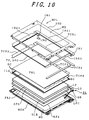
- Fig. 10 is an exploded perspective diagram for explaining the entire structure of the active matrix type liquid crystal display device using an orientation film according to the invention.
- Fig. 10 explains the specific structure of the liquid crystal display device (or the module having a liquid crystal display panel, a circuit substrate, a back light and other components integrated, as will be called the "MDL") according to the invention.
- Reference letters SHD designate a shield case (as also called the "metal frame") made of a metal sheet; letters WD a display window; letters INS1 to INS3 insulating sheets; letters PCB1 to PCB3 circuit substrates (of which: PCB1 a drain side circuit substrate and a video signal line driving circuit substrate; PCB2 a gate side circuit substrate; and PCB3 an interface circuit substrate); letters JN1 to JN3 joiners for joining the circuit substrates PCB1 to PCB3 electrically; letters TCP1 and TCP2 take carrier packages; letters PNL a liquid crystal display panel; letters GC a rubber cushion; letters ISL a shielding spacer; letters PRS a prism sheet; letters SPS a scattering sheet; letters GLB a light guide board; letters RFS a reflection sheet; letters MCA a lower case (or mold frame) formed by the integral molding; letters MO an opening of the MCA; letters LP a fluorescent lamp; letters LPC a lamp cable; letters GB a rubber bushing for
- the liquid crystal display module MDL includes two kinds of accommodating/holding members of the lower case MCA and the shield case SHD and is constructed by integrating the metallic shield case SHD accommodating and fixing the insulating sheets INS1 to INS3, the circuit substrates PCB1 to PCB3 and the liquid crystal display panel PNL, and the lower case MCA accommodating the back light BL composed of the fluorescent lamp LP, the light guide board GLB and the prism sheet PRS.
- the video signal line driving circuit substrate PCB1 On the video signal line driving circuit substrate PCB1, there is mounted an integrated circuit chip for driving the individual pixels of the liquid crystal display panel PNL.
- the interface circuit substrate PCB3 On the other hand, there are mounted an integrated circuit chip for receiving video signals from an external host and control signals such as timing signals and a timing converter TCON for generating clock signals by processing the timings.
- the clock signals are fed through a clock signal line CLL, as laid on the interface circuit substrate PCB3 and the video signal line driving circuit substrate PCB1, to the integrated circuit chip which is mounted on the video signal line driving circuit substrate PCB1.
- the interface circuit substrate PCB3 and the video signal line driving circuit substrate PCB1 are multi-layered wiring substrates, and the clock signal line CLL is formed as an inner wiring line of the interface circuit substrate PCB3 and the video signal line driving circuit substrate PCB1.
- the liquid crystal display panel PNL is constructed by adhering two substrates of the TFT substrate having TFTs and various wiring lines/electrodes and the filter substrate having the color filter and by sealing the liquid crystal in the clearance between the two substrates, such that the drain side circuit substrate PCB1 for driving the TFTs, the gate side circuit substrate PCB2 and the interface circuit substrate PCB3 are connected by the tape carrier packages TCP1 and TCP2, and such that the individual circuit substrates are connected by the joiners JN1, JN2 and JN3.
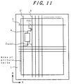
- Fig. 11 is a schematic diagram for explaining the wired structure in the vicinity of one pixel of the TFT substrate constructing the liquid crystal display device shown in Fig. 10.
- Reference numeral 1 designates a substrate; numeral 2 a scanning signal line (or gate line); numeral 2' an adjacent scanning signal line (or adjoining gate line); numeral 3 a video signal line (or drain line); numeral 4 a source electrode; numeral 6 a pixel electrode; letters TFT a thin film transistor; and letters Cadd a capacity added element.
- the central portion of the substrate 1 excepting the periphery provides a display region which is filled up with a liquid crystal in the clearance which is formed by adhering the other substrate or the filter substrate to it.
- the scanning signal line 2 (or gate line) extending in an X-direction
- the video signal line 3 (or drain line) extending in a Y-direction
- the source electrode which extends in the Y-direction while being insulated from the scanning signal fine 2 and also extends in the X-direction.
- the region as defined by those scanning signal line 2 and video signal line 3, forms one for each pixel.
- the aforementioned display region is formed of a set of numerous pixel regions arranged in a matrix shape.
- Each pixel region is composed of: the thin film transistor TFT to be turned On when the scanning signal is fed from the scanning signal line 2 and the video signal line 3; and the pixel electrode 6 to be fed from the video signal from the video signal line 3 through the thin film transistor TFT turned ON.
- the capacity added element Cadd between the adjoining scanning signal line 2' other than the scanning signal line 2 for driving the thin film transistor TFT and the aforementioned pixel electrode 5.
- This capacity added element Cadd is provided for storing the video signal for a long time in the pixel electrode 5 even when the thin film transistor TFT is turned OFF.
- the aforementioned various wiring lines for selecting the pixels are formed over the substrate 1 by using various filming means and patterning means.
- a refractory metal which has few hillocks.
- This wiring material can be exemplified by chromium (Cr) or molybdenum (Mo) as a pure metal.
- An alloy material to be used is exemplified by an alloy of the Cr and the Mo or an alloy of the Mo and tungsten (W).
- the Cr is excellent in the adhesion to the substrate and the resist and is featured in that the etching end portion is worked at a right angle with respect to the substrate face when the wiring line is etched.
- the wiring lines (or lower layer wiring lines) are formed in the lowermost layer of the substrate by using the material of such characteristics, the so-called “step coverage" at the vertical wall of the etching end is deteriorated by the insulating film or the like, as formed over the lower wiring lines. This causes problems such as the deterioration in the breakdown voltage or the disconnection of the portions where the lower wiring lines are crossed over by other wiring lines (or upper wiring lines) formed over the former.
- Fig. 12 is a partial section for explaining the structure in the vicinity of the TFT of an example of the construction of the liquid crystal display device of the prior art.
- reference numeral 1 designates a TFT substrate; numeral 1' a filter substrate; numeral 2 a scanning signal line (or gate electrode); numeral 3 a video signal line (or drain electrode 3); numeral 4 a source electrode; numeral 5 a pixel electrode; numeral 6 an insulating film; numeral 7 a semiconductor layer; numeral 7A a contact layer; numeral 8 a passivation film; numeral 8A a contact hole; numeral 9 a color filter; numeral 10 a black matrix; numeral 11 a smoothing layer; numeral 12 a common electrode; letters TFT a thin film transistor; letters Cadd a capacity added element; and letters LC a liquid crystal.
- the gate electrode 2, the insulating film 6, the semiconductor layer 7, the contact layer 7A, the drain electrode 3, the source electrode 4, the passivation film 8, the pixel electrode 5 and so on are stacked in a multilayered structure by filming them and by the patterning of the etching treatment.
- the adjoining gate electrode 2', the insulating film 6, the passivation film 8 and the pixel electrode 5 are likewise laminated.
- the gate electrode 2, as formed in the lowermost layer of the substrate 1 is made of either the pure Cr or the Cr-Mo alloy and is worked at its end portion (or side end face) at a right angle with respect to the face of the substrate 1 by the etching treatment.
- the insulating film 6, as formed thereover is insufficiently covered at its edge portion, as shown, by the normal wall face.
- the drain electrode 3 and the source electrode 4 Over the insulating film 6, there are formed the drain electrode 3 and the source electrode 4. At the portions where these drain electrode 3 and source electrode 4 ride over the gate electrode 2, the insulation gap or the film thickness becomes short, as shown, to cause the problems of the drop in the break-down voltage, the short-circuiting or the disconnection.
- the wiring line made of the pure Cr is troubled by the problem that its upper face is exposed to the dry etching atmosphere to produce a fluoride hereby to deteriorate the contact characteristics with the film formed thereover.
- the wiring line is made of the Mo-W alloy, the adhesion to the bed or substrate is weakened to raise a problem that the wiring line is easily separated by the thermal hysteresis after filmed.
- the adhesion to the substrate is similar to that which is obtained by using the Cr-Mo alloy material of the prior art.
- the problem of the step coverage has been solved, the problem of the separation of the wiring line from the substrate is still left unsolved so that a sufficient reliability cannot be achieved.
- An object of the invention is to solve the aforementioned various problems of the prior art and to provide a liquid crystal display device which is enabled to improve the reliability by satisfying the contact characteristics between the lower layer wiring line and the upper conductor film, by sufficing the step coverage of the upper film such as the insulating film, by satisfying the adhesion to the substrate and by preventing the cutting of the upper layer wiring line and the short-circuiting of the lower layer wiring line.
- the invention utilizes the difference in the corrosion rate due to the corrosion potential difference between different kinds of metals and is characterized by adopting the following means (1) to (7):
- the lower pure Cr layer is featured to have an excellent adhesion to the substrate or the bed layer.
- the upper layer of the Cr-Mo alloy is enabled to have a lower specific resistance of the materials and a lower contact resistance to the upper layer than those of the pure Cr layer by making the Mo and Cr having low specific resistance into the alloy.
- Another advantage is that the film stress can be drastically lowered, as compared with the pure Cr layer, by making the alloy of Mo and by optimizing the sputtering condition.
- the interface between the upper layer and te lower layer is etched earlier than the lower layer due to the corrosion potential difference, i.e., by the electrochemical reaction inbetween when the two layers are dipped in the common etchant.
- the side etching proceeds fastest at the interface between the upper and the lower layer. As a result, the side etching proceeds in the upper layer but proceeds earlier at the upper portion than at the lower portion in the lower layer.
- Fig. 5 is a schematic diagram for explaining a state in which the etching is proceeded by the electrochemical reaction with a difference in the corrosion potential between the upper layer and the lower layer.
- a wiring layer having a two-layered laminated structure is formed over the substrate 1 and is composed of a first layer 2A and a second layer 2B.
- the first layer or the lower layer is made of pure chromium (Cr)
- the second layer or the upper layer is made of an chromium-molybdenum (Cr-Mo) alloy.
- the etching rate takes its maximum at the interface between the upper and lower layers so that the lower layer 2A is worked at its whole side end face into a right-tapered shape whereas the upper layer 2B is worked at its side end face into either a shape normal to the face of the substrate 1 or a slightly counter-tapered shape.
- the side-etching of the upper layer has to proceed even while the lower layer is being etched.
- the corrosion potential different of the two layers is excessively large, moreover, the upper layer is exclusively etched abruptly, but the lower layer is not proceeded in its etching or takes a small taper angle if etched. It has been experimentally found out that the desirable corrosion potential difference between the upper and lower layers is set at 3 mV to 300 mV.
- the desired taper angle has been achieved within that range, especially from 5 mV to 200 mV.
- the wiring line having the desired taper shape can be formed by making the upper layer and the lower layer into the laminated structure even if the etching rate of the composition of the lower layer is higher than that of the upper layer.
- the combination of the first and second layers may be other than that of the pure Cr and the Cr-Mo alloy. Similar effects can also be obtained from the laminated structure which is made of a Cr-W alloy and the pure Cr by adding W in place of Mo. Moreover, the corrosion potential difference of the two layers may be controlled by adding different second elements to the two layers.
- the corrosion potential difference can be established between the layers of the laminated structure to give the individual layers functions other than the corrosion potential.
- the film stress can be lowered in the first layer, and the contact resistance to the overlying layer can be reduced in the second layer.
- the defects in the step coverage of the film to be formed over the upper layer can be avoided even if the upper layer has a side end face set at a right angle or counter-tapered with respect to the substrate face.
- Fig. 6 is an explanatory diagram of a change in the length of cracks to extend in the CVD film formed in the gate wiring portion when the film ratio between the upper layer and the lower layer is changed.
- the abscissa indicates the ratio a/b between the film thickness a of the lower layer and the film thickness b of the upper layer, and the ordinates indicates the crack length (nm).
- letters CL designate cracks.
- the thickness of the film to be formed as the insulating film 6 by the CVD is usually 300 to 400 nm.
- the thickness a of the upper layer is larger than that b of the lower layer, that is, when the ratio a/b is no less than 1, the coverage of the gate electrode 2 with the insulating film 6 is so poor as to cause the long racks.
- the cracks can be completely eliminated or reduced to a state of no practical problem.
- the film thickness of the lower layer 2A is set to 200 nm, for example, an excellent coverage having no substantial crack can be realized for the film thickness of the upper layer 2B no more than 60 nm.
- the film thickness indispensable for forming the thin film all over the substrate is 10 nm or more, however, it is desired to set the film thickness of the upper layer 2B at a value from 10 nm to 60 nm.
- the film thickness of the upper layer must be thickner than 60nm, the combination of taper-etching which utilize electrochemical reaction and another taper-etching method which utilize penetration of etchant at the interface between photo-versist and the upper layer is available.
- Fig. 7 is an explanatory diagram of the result of a change, as measured by changing a Mo concentration, in the corrosion potentials of the pure Cr and the Cr-Mo alloy in an aqueous solution of ceric nitrate.
- the corrosion potential is at 1,150 mV for the pure Cr, that is, when the Mo concentration is 0, and at 1,100 mV for the alloy containing Cr-50 Wt. % of Mo.
- the corrosion potential of the pure Mo is as low as 360 mV so that the corrosion potential of the Cr-Mo alloy becomes the lower for the higher Mo concentration.
- Fig. 8 is an explanatory diagram of a change in a taper angle when the composition of the Cr-Mo alloy to be combined with the pure Cr is changed.
- the wiring line is exclusively made of Cr so that the taper angle takes a value of 90 degrees (or normal to the substrate face).
- the taper angle is lowered so that the taper angle of 40 to 60 degrees by adding 10 to 65 % of Mo.
- the taper angle is 55 degrees.
- the Mo concentration of the upper layer rises to increase the corrosion potential difference between the two layers, the taper angle of the lower layer is hardly changed, but the upper layer takes the counter-tapered tendency to have a poor entire shape. It is therefore recommended that the Mo concentration is selected within a range of 10 Wt. % to 60 Wt. %.
- the taper angle may be dispersed so largely reflecting the interface dispersion of the adhesion between the photoresist and the metallic thin film as to be doubled between the central portion and the peripheral portion.
- the aforementioned corrosion potential difference is determined by the material employed. According to the invention making use of the potential difference between the upper layer film and the lower layer film, therefore, the in-face dispersion of the taper angle of the etching treatment can be so limited within ⁇ 9 %.
- the step coverage of an insulating film (or gate insulating film), an a-Si semiconductor film or a drain wiring line of SiN to be formed over the gate wiring line is improved to raise the breakdown voltage and to reduce the percent defective such as the disconnection of the drain wiring line.
- the upper layer containing the added Mo is hard to remain a fluoride and to oxidize in the oxidizing atmosphere, even dry-etched with a fluorine containing gas, so that its contact with another over electrode can be kept satisfactory.
- the two layers for establishing she corrosion potential difference between the laminated films need not directly contact at all times, but similar effects can be achieved if the two layers are in contact through a conductive layer. It is therefore possible to make a three-layered structure in which a conductor layer of Al to be selectively etched with Cr is sandwiched between the Cr layer and the Cr-Mo layer. At this time, when the uppermost Cr layer is etched at the time of etching the lowermost Cr layer or Cr-Mo layer, the electrochemical reaction can be effected inbetween to etch one of them backward in a preferential manner. The shape to be obtained becomes difference depending upon which of Cr and Cr-Mo is employed as the uppermost layer, as shown in Fig. 9.
- Figs. 9A to 9C are explanatory diagrams of etched shapes of the two- or three-layered structure.
- a film having a low corrosion potential is employed as the uppermost layer, as shown in Fig. 9A, the uppermost layer retracts from the Al, but this retraction can be suppressed.
- the overhang of the Al from the lower layer of Cr can be reduced to smooth the entire wiring line as a whole.
- the retraction of the lowermost layer is promoted whereas the retraction of the uppermost layer is suppressed, as shown in Fig. 9B.
- the Al surface other than the end portion can be covered with the Cr to suppress the growth of a hillock of the Al from the end portion.
- the film construction may be made, as shown in Fig. 9A.
- the film construction may be made, as shown in Fig. 9B.
- Fig. 9C shows an example of the prior art, in which only the A l layer protrudes to raise the problems in the entire shape and the anti-hillock.
- Fig. 1 is a partial section for explaining an essential structure of a liquid crystal display device according to the invention
- Fig. 2 is a partial top plan view for explaining an essential structure of the same.
- reference numeral 1 designates a TFT substrate; numeral 1' a filter substrate; numeral 2 a gate electrode; numeral 3 a drain electrode; numeral 4 a source electrode; numeral 5 a pixel electrode; numeral 6 an insulating film; numeral 7 a semiconductor layer; numeral 7A a contact layer; numeral 8 a passivation film; numeral 8A a contact hole; numeral 9 a color filter; numeral 10 a black matrix; numeral 11 a smoothing layer; letters TFT a thin film transistor; letters Cadd a capacity added element; and letters LC a liquid crystal.
- numerals 3A and 3B, and 4A and 4B designate the laminated portions of a Cr-Mo alloy layer and pure Cr constructing the drain electrode 3 and the source electrode 4, respectively.
- numerals 2A and 2B designate a first layer (or lower layer) and a second layer (or upper layer) constructing the gate electrode 2.
- the lower layer 2A is the pure Cr layer whereas the upper layer 2B is the Cr-Mo alloy layer. Moreover, the lower layer 2A is given a thickness of 150 nm whereas the upper layer 2B is given a thickness of 50 nm, and the side end face of the wiring line is mostly right-tapered in a satisfactory manner.
- the side end face of the upper layer 2B is shaped vertically of the substrate face, as shown in Fig. 1, but has the small thickness so that the entire wiring line exerts no substantial influence on the right-tapered shape.
- the gate electrode 2 is thus given the laminated structure having the first layer of pure Cr satisfactorily right-tapered, it is possible to prevent the drain electrode 3 and the source electrode 4 to be formed thereover from being broken and to avoid a disadvantage that either cracks or pin holes are formed in the insulating film 6. since the lower layer contacting with the substrate is made of the pure Cr layer, moreover, the adhesion between the gate electrode 2 and the substrate can be enhanced to prevent the separation of the wiring line, as might otherwise be caused by the thermal stress or the like.
- SiN silicon nitride
- the thin film transistor TFT Over the insulating film 6 at one corner of the pixel region which is defined by the gate electrode 2, the drain electrode 3 and the source electrode 4, moreover, there is formed the thin film transistor TFT. In the region forming this thin film transistor TFT, there is formed as the upper layer of the insulating film 6 and on the surface of the insulating film 6, as located over the gate electrode 2, the semiconductor layer 7 which is made of amorphous silicon (a-Si) crossing the gate electrode 2.
- a-Si amorphous silicon
- this semiconductor layer 7 is formed to act as the lower layer of the region forming the source electrode 4.
- the laminated structure of the source electrode 4 over the semiconductor layer 7 is provided for preventing the benching and for reducing the capacity between itself and the intersecting gate electrode 2.
- the drain electrode 3 and the source electrode 4 which are arranged to confront each other through the gate electrode 2, as viewed in a top plan view.
- the contact layer 7A which is made by doping the semiconductor layer 7 with an impurity of high concentration.
- This highly doped impurity layer is formed all over the semiconductor layer 7, when this layer 7 is formed, by etching the impurity layer, as exposed from the electrodes 3 and 4 to be formed later, by using the electrodes 3 and 4 as the masks.
- drain electrode 3 and the source electrode 4 are formed at the same step and of the same material.
- This material is exemplified by a laminated wiring line shared with the gate electrode 2.
- Another example may be a single alloy layer of Cr and Mo.
- the source electrode 4 extends so long as the region to form the pixel electrode 5 and makes a contact with pixel electrode 5 at this extension.
- the source electrode 4 is made of the material shared with the drain electrode 3 and is formed of the laminated structure of the laminated structure of the layers 3B and 4B of the Cr-Mo alloy and the layers 3A and 4B of Cr.
- the passivation film 8 which is made of a silicon nitride (SiN) film, for example, so as to avoid the direct contact of the liquid crystal with the thin film transistor TFT.
- the contact hole 8A for exposing a portion of the extension of the source electrode 4.
- the pixel electrode 5 which is made of an ITO film, for example.
- This pixel electrode 5 can be electrically connected with the source electrode 4 through the contact hole 8A.
- the pixel electrode 5 is partially extended to over another adjoining gate electrode 2' which is different from the gate electrode 2 for driving the thin film transistor TFT.
- the capacity added layer Cadd is constructed of a dielectric film of the laminated structure which is composed of the insulating film 6, as sandwiched between the pixel electrode 5 and the adjoining gate electrode 2', and the passivation film 8.
- the substrate 1 thus having the various films is adhered through the liquid crystal LC to the other substrate (or transparent substrate) 1', as shown in Fig. 1.
- the substrate 1' on the liquid crystal LC there are formed by the ITO the plural color filters 9, which are defined by the black matrix 10, and the common electrode 12 which is shared among the individual pixel regions through the smoothing layer 11 covering that color filters 9.
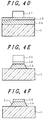
- Figs. 3A to 3C and Figs. 4D to 4F are schematic step diagrams for explaining the example of the process for manufacturing the liquid crystal display device according to the invention, and the same reference numerals as those of Figs. 1 and 2 correspond to the common portions.
- the first layer (or lower layer) 2A of pure Cr is filmed (as shown in Fig. 3A) to have a thickness of 150 nm all over the principal surface of the glass substrate 1 by using the sputtering method or the like.
- the alloy layer containing 50 Wt. % of Cr and Mo is filmed (as shown in Fig. 3B) to form the second layer (or upper layer) 2B having a thickness of 50 nm over the first upper layer by the sputtering method or the like thereby to form the laminated structure mainly for the Cr wiring line.
- This laminated structure provides the gate electrode 2.
- a photoresist 20 is applied (as shown in Fig. 3C) to all over the upper face of the laminated structure and is selectively exposed through a photo mask 20a having a pattern of a gate electrode terminal 2C or the like of the thin film transistor TFT to be formed integrally with the gate electrode 2.
- the photoresist 20 is developed (as shown in Fig. 4D) to remove its portion corresponding to the region other than those to form the gate electrode 2,the gate electrode terminal 2C and so on, thereby to expose the laminated structure of the removed portion.
- the exposed laminated structure is dipped in the etchant for the etching treatment.
- This etchant is exemplified by an aqueous solution of ceric nitrate and ammonia.
- the upper and lower layers making the laminated structure have the corrosion potentials of 1,100 mV and 1,150 mV, respectively, for the upper alloy layer of 50 Wt. % of Cr and Mo and the lower layer of pure Cr, so that a potential difference of 50 mV is established inbetween.
- the corrosion potential of the upper layer lower than that of the lower layer, the interfacial layer having the lower corrosion potential can be etched (as shown in Fig.
- the upper layer is given a thickness of 50 nm whereas the lower layer is given a thickness of 150 nm.
- the photoresist 20 is removed (as shown in Fig. 4F) to form the gate electrode 2, the gate electrode terminal 2C and so on with the laminated film which is left after the etching treatment.
- the substrate 1 thus having the gate electrode 2 and the gate electrode terminal 2C formed by the aforementioned steps is worked to form the thin film transistor TFT by the following steps.
- the substrate 1 having the gate electrode 2 and gate electrode terminal 2C formed by the aforementioned individual steps is formed all over its principal face sequentially with the insulating layer 6 made of a silicon nitride, the semiconductor layer 7 of i-type amorphous Si and an amorphous Si semiconductor contact layer 7A doped with an n-type impurity, for example, by using the CVD method.
- the manufacture process can be simplified by sequentially forming the insulating layer 6, the semiconductor layer 7 and the semiconductor contact layer 7A doped with the n-type impurity, in the continuous manner. Since the gate electrode 1C shown in Fig. 1 is laminated in its entirety at this time, the coverage of the gate insulating film to be formed by the CVD over the gate electrode 1c is improved to avoid the defect of the gate insulating film and the short-circuiting and disconnection between the drain line or the source electrode to be formed over the gate insulating film and the gate electrode.
- the photoresist film is applied to the whole area of the upper face of the semiconductor contact layer 7A doped with the n-type impurity and is selectively exposed through the photo mask having the pattern of the thin film transistor TFT.
- the photoresist film is developed to remove its portion other than the region for forming the thin film transistor TFT, thereby to expose the upper face of the semiconductor contact layer 7A, as doped with the n-type impurity, from that removed portion.
- the residual photoresist film is used as the mask to selectively etch the semiconductor contact layer 7A, as exposed from that mask, and the underlying semiconductor layer 7.
- the insulating layer 6, as located below the semiconductor layer 7, is not etched but left.
- the silicon nitride film for the gate insulating layer As a result, in the region for forming the thin film transistor TFT, there are sequentially formed the silicon nitride film for the gate insulating layer, the i-type amorphous Si semiconductor layer, and the amorphous Si semiconductor layer doped with the n-type impurity for the contact layer.
- the semiconductor contact layer 7A As doped with the n-type impurity, and the semiconductor layer 7.
- the laminated structure of the Cr-Mo alloy layer and the pure Cr layer by the sputtering method, for example.
- This laminated structure exposes the photoresist selectively through the photo mask which has the pattern including the source electrode 4, the drain electrode 3 and the drain electrode terminal 3b.
- the photoresist film is developed to remove the photoresist film corresponding to the region other than those for forming the source electrode 4, the drain electrode 3 and the drain electrode terminal 3B, thereby to expose the aforementioned alloy film from the removed portions.
- the alloy layer, as exposed from this mask, is selectively etched.
- the source electrode 4, the drain electrode 3 and the drain electrode terminal 3B are formed from the remaining alloy layer.
- the semiconductor contact layer 7A as overlying the semiconductor layer 7 formed in the region to form the thin film transistor TFT and as doped with the n-type impurity, is selectively etched by using the source electrode 4 and the drain electrode 3 as the mask.
- the semiconductor contact layer 7A as left and doped with the n-type impurity, is formed only in the interface for the semiconductor layer 7 between the source electrode 4 and the drain electrode 3 so that it functions as the contact layer 7A.
- the passivation film 8 of the silicon nitride is formed by the plasma CVD method, for example, all over the principal surface of the substrate 1 worked by the aforementioned individual steps.
- the side end edges of the source electrode 4 and the drain electrode 3 are wholly right-tapered profiling the shape of the underlying gate electrode 2.
- the step coverage by the passivation film 8 can be improved to reduce the film defects such as the pin holes at the riding portions of the gate electrode and the drain wiring line at the passivation film 8. Since the gate electrode and the drain electrode are worked to have the right taper, moreover, the step on the surface at the portion to form the thin film transistor TFT is made gentle.
- the contact hole 8A is formed in the passivation film 8. Simultaneously with this, openings are formed in both the passivation film 8 formed over the drain electrode terminal 3B and the passivation film 8 formed over the gate electrode terminal 2C.
- the mask as used for working the passivation film 8, is employed as it is to perform the dry etching.
- the through hole is formed in the insulating layer 6 to expose the surface of the substrate 1 at the gate electrode terminal 2C, the drain electrode terminal 3B and the desired region.
- the electrode surface is exposed to that gas during the over-etching time. Since this source electrode surface is made of the Cr-Mo alloy layer, less fluoride or chloride is formed than the case of the pure Cr layer so that the contact characteristics with the overlying ITO film can be drastically improved.
- This ITO film is given a suitable thickness of 70 to 300 nm, as exemplified here by 40 nm.
- the photoresist film is formed all over the surface of the ITO film and is selectively exposed through the photo mask having the pattern including the pixel electrode 5, the gate electrode and the drain electrode terminal.
- the photoresist film is developed to remove its portion other than the region for forming the pixel electrode 5, the individual gate electrodes and the drain electrode terminal.
- the residual photoresist mask is used as the mask to selectively etch the ITO film exposed from the mask. As a result, the pixel electrode 5 and so on are formed from the residual ITO film.
- the filter substrate 1' as shown in Fig. 1, is adhered to the TFT substrate having the desired wiring lines and electrodes formed by the aforementioned individual steps, and the clearance inbetween is filled with the liquid crystal LC to form the liquid crystal panel.
- the liquid crystal panel thus prepared is assembled with the various components, as described with reference to Fig. 10, to provide the liquid crystal display device.
- any combination other than that of the pure Cr and the Cr-Mo alloy can be adopted if it gives a difference in corrosion potential between the lower layer portion and the upper layer portion.
- This condition can be satisfied to effect the taper-etching even if the upper layer is made of a Cr-W alloy whereas the lower layer is made of the pure Cr, for example.
- the same condition can also be satisfied to effect the taper-etching even if the upper layer is made of the Cr-Mo alloy whereas the lower layer is made of the Cr-W alloy.
- the satisfactory taper-etching can be effected, when the upper layer portion is made of the alloy containing 50 Wt. % of Cr and Mo whereas the lower layer portion is made of a Cr-W alloy containing 40 Wt. % or more of W.
- the above-specified Cr can be replaced in a single or alloy state by a metallic material for an electrode material having the working characteristics, as noted by the invention, such as aluminum (Al), titanium (Ti), tungsten (W) or molybdenum (Mo).
- a metallic material for an electrode material having the working characteristics such as aluminum (Al), titanium (Ti), tungsten (W) or molybdenum (Mo).
- the taper-etching treatment using a similar mechanism can be performed for the individual materials by adding a second element to each of the metals and by laminating it and the composition which is controlled in the corrosion potential in each etchant.
- a satisfactory tapered shape can be given especially to the side end face of the scanning signal line to be formed at the thin film transistor TFT thereby to prevent the film defects such as the cracks, pin holes or disconnections of the various thin films overlying the scanning signal line, and the short-circuiting between the upper and lower layers.
- the contact of the other scanning signal lines and the electrodes to be formed thereover and the metallic thin film is improved.
- the adhesion with the substrate is enhanced to prevent the film separation which might otherwise be caused the thermal hysteresis or stress at the subsequent working step.
- the surface of the thin film transistor substrate can be smoothed to reduce the orientation defects or the like of the liquid crystal thereby to provide a liquid crystal display layer having an excellent contrast.
- the invention should not be limited to the so-called “longitudinal field type liquid crystal display device”, as has been described in connection with the embodiment, but can likewise be applied to the so-called “transverse field type liquid crystal display device", in which the common electrode is also formed on the side of the active matrix substrate, or another type liquid crystal display device having the crossing portion, across which the electrode wiring lines or the like cross each other, or a variety of similar semiconductor devices.
Abstract
Description
wherein the wiring line of at least said signal lines comprises a wiring line of a laminated structure formed on the side of said one substrate, wherein said laminated structure including a first layer made of a first metal layer and a second layer formed over said first layer and made of a second metal layer having the same principal component as that of said first metal layer but a different added element and/or a different composition, and wherein said first layer has a side end face of a right-tapered shape whereas said second layer has a side end face set at a right angle or counter-tapered with respect to the substrate face;
wherein the wiring line of at least said signal lines comprises a laminated structure formed on the side of said one substrate, wherein said laminated structure including a first layer containing chromium and tungsten as its principal component and a second layer formed over said first layer and made of chromium and molybdenum as its principal component, and wherein said first layer has a side end face of a right-tapered shape whereas said second layer has a side end face set at a right angle or counter-tapered with respect to the substrate face;
wherein the wiring line of at least said signal lines comprises a three-layered laminated structure formed on the side of said one substrate, wherein either the first layer or the third layer contains two kinds of metals having the same principal component but a different added element and/or a difference composition, wherein said second layer is made of a metal having a principal component other than those of said first and third layers and capable of being selectively etched from said first and third layers, and wherein either of said first layer or said second layer is more etched back than the other;
Claims (4)
- A liquid crystal display device (MDL) comprising: a pair of substrates, a liquid crystal layer (LC) interposed between said pair of substrates (1), a wiring line (2) including a first layer (2A) and a second layer (2B) formed on one of said substrates,
wherein said first layer (2A) has a side end face of a righttapered shape and said second layer (2B) has a side end face set at a right angle or counter-tapered with respect to the substrate face. - A liquid crystal display device (MDL) according to claim 1, wherein said first layer (2A) is made of a pure chromium layer and said second layer (2B) is made of an alloy layer containing chromium and molybdenum as its principal component.
- A liquid crystal display device (MDL) comprising: a pair of substrates (1), a liquid crystal layer (LC) interposed between said pair of substrates, a wiring line (2) including a first layer (2A), a second layer (2B), and a third layer formed on one of said substrates,
wherein said first layer (2A) has a side end face of a righttapered shape and said third layer has a side end face set at a right angle or counter-tapered with respect to the substrate face. - A liquid crystal display device (MDL) according to claim 3, wherein said first layer (2A) is made of a pure chromium layer and said second layer (2B) is made of an alloy layer containing aluminum and said third layer is made of an alloy layer containing chromium and molybdenum as its principal component.
Applications Claiming Priority (2)
| Application Number | Priority Date | Filing Date | Title |
|---|---|---|---|
| JP155238/97 | 1997-06-12 | ||
| JP9155238A JP2985124B2 (en) | 1997-06-12 | 1997-06-12 | Liquid crystal display |
Publications (2)
| Publication Number | Publication Date |
|---|---|
| EP0884624A2 true EP0884624A2 (en) | 1998-12-16 |
| EP0884624A3 EP0884624A3 (en) | 1999-05-06 |
Family
ID=15601565
Family Applications (1)
| Application Number | Title | Priority Date | Filing Date |
|---|---|---|---|
| EP98110342A Withdrawn EP0884624A3 (en) | 1997-06-12 | 1998-06-05 | Liquid crystal display device |
Country Status (5)
| Country | Link |
|---|---|
| US (1) | US6404473B1 (en) |
| EP (1) | EP0884624A3 (en) |
| JP (1) | JP2985124B2 (en) |
| KR (1) | KR100643960B1 (en) |
| TW (2) | TW557392B (en) |
Cited By (1)
| Publication number | Priority date | Publication date | Assignee | Title |
|---|---|---|---|---|
| US7799590B2 (en) | 2000-01-26 | 2010-09-21 | Semiconductor Energy Laboratory Co., Ltd. | Semiconductor device and manufacturing method thereof |
Families Citing this family (21)
| Publication number | Priority date | Publication date | Assignee | Title |
|---|---|---|---|---|
| TW480554B (en) * | 1999-07-22 | 2002-03-21 | Semiconductor Energy Lab | Semiconductor device and manufacturing method thereof |
| KR100504531B1 (en) * | 1999-12-15 | 2005-08-03 | 엘지.필립스 엘시디 주식회사 | An in-plane switching mode liquid crystal display device |
| KR100660811B1 (en) * | 1999-12-31 | 2006-12-26 | 엘지.필립스 엘시디 주식회사 | method of fabricating electro line for liquid crystal display |
| JP2008083731A (en) * | 2000-01-26 | 2008-04-10 | Semiconductor Energy Lab Co Ltd | Semiconductor device |
| KR100628257B1 (en) * | 2000-10-20 | 2006-09-27 | 엘지.필립스 엘시디 주식회사 | The Structure of the reflective type and the semi-transparent type Liquid Crystal Display device |
| JP2002245947A (en) * | 2000-12-15 | 2002-08-30 | Canon Inc | Substrate with thin line, manufacturing method thereof, electron source substrate and image display device |
| KR100796749B1 (en) | 2001-05-16 | 2008-01-22 | 삼성전자주식회사 | A thin film transistor array substrate for a liquid crystal display |
| KR20030016051A (en) * | 2001-08-20 | 2003-02-26 | 삼성전자주식회사 | Thin film transistor array panel for a liquid crystal display and a manufacturing method thereof |
| US6853173B2 (en) * | 2002-01-25 | 2005-02-08 | Broadcom Corporation | Programmable dual mode hysteretic power output controller |
| KR100905472B1 (en) * | 2002-12-17 | 2009-07-02 | 삼성전자주식회사 | Thin film transistor array panel and liquid crystal display including the panel |
| KR100939560B1 (en) * | 2003-06-30 | 2010-01-29 | 엘지디스플레이 주식회사 | Liquid Crystal Display and method for fabricating of the same |
| KR100543001B1 (en) * | 2003-09-03 | 2006-01-20 | 삼성에스디아이 주식회사 | TFT and Active Matrix FPD |
| AT500259B1 (en) * | 2003-09-09 | 2007-08-15 | Austria Tech & System Tech | THIN-LAYER ASSEMBLY AND METHOD FOR PRODUCING SUCH A THIN-LAYER ASSEMBLY |
| JP2006148050A (en) * | 2004-10-21 | 2006-06-08 | Seiko Epson Corp | Thin film transistor, electro-optical device and electronic equipment |
| KR101219037B1 (en) * | 2005-07-01 | 2013-01-09 | 삼성디스플레이 주식회사 | Thin film panel and manufacturing method thereof |
| JP5066836B2 (en) * | 2005-08-11 | 2012-11-07 | セイコーエプソン株式会社 | Electro-optical device and electronic apparatus |
| JP5234301B2 (en) * | 2005-10-03 | 2013-07-10 | Nltテクノロジー株式会社 | Thin film transistor, thin film transistor array substrate, liquid crystal display device and manufacturing method thereof |
| KR101319301B1 (en) * | 2006-12-15 | 2013-10-16 | 엘지디스플레이 주식회사 | Liquid crystal display device and method for fabricating the same |
| JP5250832B2 (en) | 2007-07-09 | 2013-07-31 | ゴールドチャームリミテッド | Active matrix drive display device |
| KR101984218B1 (en) * | 2011-01-28 | 2019-05-30 | 가부시키가이샤 한도오따이 에네루기 켄큐쇼 | Method for manufacturing semiconductor device and semiconductor device |
| JP2016099492A (en) | 2014-11-21 | 2016-05-30 | セイコーエプソン株式会社 | Liquid crystal device and electronic apparatus |
Citations (3)
| Publication number | Priority date | Publication date | Assignee | Title |
|---|---|---|---|---|
| EP0680079A2 (en) * | 1994-04-28 | 1995-11-02 | Xerox Corporation | Thin-film structure tapered feature |
| US5464500A (en) * | 1993-08-06 | 1995-11-07 | International Business Machines Corporation | Method for taper etching metal |
| EP0812012A1 (en) * | 1996-06-07 | 1997-12-10 | Lucent Technologies Inc. | Method for etching to produce metal film structures having tapered sidewalls |
Family Cites Families (12)
| Publication number | Priority date | Publication date | Assignee | Title |
|---|---|---|---|---|
| JP2620240B2 (en) * | 1987-06-10 | 1997-06-11 | 株式会社日立製作所 | Liquid crystal display |
| EP0430702B1 (en) * | 1989-11-30 | 1999-01-13 | Kabushiki Kaisha Toshiba | Line material, electronic device using the line material and liquid crystal display |
| US5162933A (en) * | 1990-05-16 | 1992-11-10 | Nippon Telegraph And Telephone Corporation | Active matrix structure for liquid crystal display elements wherein each of the gate/data lines includes at least a molybdenum-base alloy layer containing 0.5 to 10 wt. % of chromium |
| JP3194274B2 (en) * | 1991-04-16 | 2001-07-30 | セイコーエプソン株式会社 | Method for manufacturing active matrix type liquid crystal display device |
| JP2952075B2 (en) * | 1991-06-12 | 1999-09-20 | キヤノン株式会社 | Liquid crystal device manufacturing method |
| JPH06177381A (en) * | 1992-12-03 | 1994-06-24 | Fujitsu Ltd | Matrix of thin film transistor and its manufacture |
| US5693983A (en) * | 1994-04-28 | 1997-12-02 | Xerox Corporation | Thin-film structure with conductive molybdenum-chromium line |
| JPH08116065A (en) * | 1994-10-12 | 1996-05-07 | Sony Corp | Thin film semiconductor device |
| JP3132310B2 (en) * | 1994-11-18 | 2001-02-05 | 株式会社日立製作所 | Active matrix type liquid crystal display |
| JPH10133216A (en) * | 1996-11-01 | 1998-05-22 | Hitachi Ltd | Active matrix type liquid crystal display device |
| JPH09197435A (en) * | 1996-01-17 | 1997-07-31 | Toshiba Corp | Liquid crystal display device and its production |
| US6208400B1 (en) * | 1996-03-15 | 2001-03-27 | Canon Kabushiki Kaisha | Electrode plate having metal electrodes of aluminum or nickel and copper or silver disposed thereon |
-
1997
- 1997-06-12 JP JP9155238A patent/JP2985124B2/en not_active Expired - Lifetime
-
1998
- 1998-06-03 TW TW087108734A patent/TW557392B/en not_active IP Right Cessation
- 1998-06-03 TW TW91108725A patent/TW573199B/en not_active IP Right Cessation
- 1998-06-05 EP EP98110342A patent/EP0884624A3/en not_active Withdrawn
- 1998-06-05 US US09/092,078 patent/US6404473B1/en not_active Expired - Lifetime
- 1998-06-12 KR KR1019980021843A patent/KR100643960B1/en not_active IP Right Cessation
Patent Citations (3)
| Publication number | Priority date | Publication date | Assignee | Title |
|---|---|---|---|---|
| US5464500A (en) * | 1993-08-06 | 1995-11-07 | International Business Machines Corporation | Method for taper etching metal |
| EP0680079A2 (en) * | 1994-04-28 | 1995-11-02 | Xerox Corporation | Thin-film structure tapered feature |
| EP0812012A1 (en) * | 1996-06-07 | 1997-12-10 | Lucent Technologies Inc. | Method for etching to produce metal film structures having tapered sidewalls |
Cited By (2)
| Publication number | Priority date | Publication date | Assignee | Title |
|---|---|---|---|---|
| US7799590B2 (en) | 2000-01-26 | 2010-09-21 | Semiconductor Energy Laboratory Co., Ltd. | Semiconductor device and manufacturing method thereof |
| US8017456B2 (en) | 2000-01-26 | 2011-09-13 | Semiconductor Energy Laboratory Co., Ltd. | Semiconductor device and manufacturing method thereof |
Also Published As
| Publication number | Publication date |
|---|---|
| TW557392B (en) | 2003-10-11 |
| KR19990006908A (en) | 1999-01-25 |
| US6404473B1 (en) | 2002-06-11 |
| JP2985124B2 (en) | 1999-11-29 |
| JPH112843A (en) | 1999-01-06 |
| KR100643960B1 (en) | 2007-03-02 |
| EP0884624A3 (en) | 1999-05-06 |
| TW573199B (en) | 2004-01-21 |
Similar Documents
| Publication | Publication Date | Title |
|---|---|---|
| US6404473B1 (en) | Display device having a wiring multi-layered structure with tapered first layer and a manufacturing process for the tapered structure | |
| KR100423564B1 (en) | LCD and its manufacturing method | |
| US5835177A (en) | Array substrate with bus lines takeout/terminal sections having multiple conductive layers | |
| CN100444013C (en) | Liquid crystal display device and fabricating method thereof | |
| CN100426108C (en) | Liquid crystal display | |
| JP3785900B2 (en) | Liquid crystal display device and manufacturing method thereof | |
| USRE39798E1 (en) | Active matrix LCD device with image signal lines having a multilayered structure | |
| US7511304B2 (en) | Substrate for display device having a protective layer provided between the pixel electrodes and wirings of the active matrix substrate and display device | |
| JP2000284326A (en) | Liquid crystal display device and its production | |
| US6731364B2 (en) | Liquid crystal display device | |
| JP2008107849A (en) | Liquid crystal display device and its manufacturing method | |
| JP2002148659A (en) | Liquid crystal display device | |
| US20030112382A1 (en) | Liquid crystal display device | |
| JP2001255543A (en) | Liquid crystal display device | |
| JPH1062818A (en) | Production of liquid crystal display device | |
| US6392721B1 (en) | Liquid crystal display device having wiring line including first and second layers with second layer having a thickness not greater than 1/2 of a thickness of first layer | |
| JP3339190B2 (en) | Liquid crystal display | |
| JP3372882B2 (en) | Method for manufacturing substrate in reflective liquid crystal display device | |
| KR20010066244A (en) | Liquid crystal display device and method for fabricating the same | |
| JPH06289423A (en) | Liquid crystal display device | |
| JPH0220830A (en) | Thin film transistor array | |
| JP2002090775A (en) | Matrix array substrate | |
| JP2001005028A (en) | Liquid crystal display device and its production | |
| KR100318540B1 (en) | Liquid Crystal Display and a Manufacturing Method thereof | |
| JP2690404B2 (en) | Active matrix substrate |
Legal Events
| Date | Code | Title | Description |
|---|---|---|---|
| PUAI | Public reference made under article 153(3) epc to a published international application that has entered the european phase |
Free format text: ORIGINAL CODE: 0009012 |
|
| AK | Designated contracting states |
Kind code of ref document: A2 Designated state(s): DE FR GB |
|
| AX | Request for extension of the european patent |
Free format text: AL;LT;LV;MK;RO;SI |
|
| PUAL | Search report despatched |
Free format text: ORIGINAL CODE: 0009013 |
|
| AK | Designated contracting states |
Kind code of ref document: A3 Designated state(s): AT BE CH CY DE DK ES FI FR GB GR IE IT LI LU MC NL PT SE |
|
| AX | Request for extension of the european patent |
Free format text: AL;LT;LV;MK;RO;SI |
|
| 17P | Request for examination filed |
Effective date: 19990408 |
|
| AKX | Designation fees paid |
Free format text: DE FR GB |
|
| 17Q | First examination report despatched |
Effective date: 20010209 |
|
| STAA | Information on the status of an ep patent application or granted ep patent |
Free format text: STATUS: THE APPLICATION IS DEEMED TO BE WITHDRAWN |
|
| 18D | Application deemed to be withdrawn |
Effective date: 20030424 |