EP0885775A2 - Electronic circuit generating electric signals delayed in time after activation of the direction indicating flasher unit of a motor vehicle - Google Patents
Electronic circuit generating electric signals delayed in time after activation of the direction indicating flasher unit of a motor vehicle Download PDFInfo
- Publication number
- EP0885775A2 EP0885775A2 EP98810455A EP98810455A EP0885775A2 EP 0885775 A2 EP0885775 A2 EP 0885775A2 EP 98810455 A EP98810455 A EP 98810455A EP 98810455 A EP98810455 A EP 98810455A EP 0885775 A2 EP0885775 A2 EP 0885775A2
- Authority
- EP
- European Patent Office
- Prior art keywords
- signal
- signals
- bit
- flashing
- debouncer
- Prior art date
- Legal status (The legal status is an assumption and is not a legal conclusion. Google has not performed a legal analysis and makes no representation as to the accuracy of the status listed.)
- Withdrawn
Links
Images


Classifications
-
- B—PERFORMING OPERATIONS; TRANSPORTING
- B60—VEHICLES IN GENERAL
- B60Q—ARRANGEMENT OF SIGNALLING OR LIGHTING DEVICES, THE MOUNTING OR SUPPORTING THEREOF OR CIRCUITS THEREFOR, FOR VEHICLES IN GENERAL
- B60Q1/00—Arrangement of optical signalling or lighting devices, the mounting or supporting thereof or circuits therefor
- B60Q1/26—Arrangement of optical signalling or lighting devices, the mounting or supporting thereof or circuits therefor the devices being primarily intended to indicate the vehicle, or parts thereof, or to give signals, to other traffic
- B60Q1/34—Arrangement of optical signalling or lighting devices, the mounting or supporting thereof or circuits therefor the devices being primarily intended to indicate the vehicle, or parts thereof, or to give signals, to other traffic for indicating change of drive direction
- B60Q1/38—Arrangement of optical signalling or lighting devices, the mounting or supporting thereof or circuits therefor the devices being primarily intended to indicate the vehicle, or parts thereof, or to give signals, to other traffic for indicating change of drive direction using immovably-mounted light sources, e.g. fixed flashing lamps
- B60Q1/382—Electronic temporisation with semiconductor amplification
Definitions
- German patent 3 442 205 Al does that automatic switch-off of the turn signal system from the driving speed dependent.
- the speed of the vehicle is from USA Patent 4,058,797 used, an extension of this Principle (USA Patent 4,333,071) closes the distance traveled Distance as well as the handlebar movement.
- a relatively simple one would be advantageous Establishment, which only after a reasonable time Delay is used and therefore can be set that they usually don't at all has to appear and only when unusual long failure to reset the turn signal Gives warning signals. The driver then remains left, at your own discretion and depending the respective traffic situation towards these signals react or negate them if necessary.
- the facility at the so-called Hazard warning flashes also after Exceeding the preset number of flashing signals or the preset delay time none Generate warning signals or do not use hazard warning flashing switch off.
- the facility is also not allowed to quick or multiple changes between left and right impair flashing.
- the facility is particularly but not exclusively, suitable for the subsequent Installation in motorcycles which already have one conventional manually switched turn signal system are without serious interference in the existing electrical or mechanical system necessary close.
- the flasher units of today's turn signal systems are mostly with electronically controlled switching relays fitted. They are also thermally controlled so-called Bimetal switch applied. According to experience can be used regardless of the choice of the used Flasher, the so-called. Bouncing of the switch contacts do not avoid this flasher. When operating the The turn signal system does not interfere with this, for operation the device according to the invention would bounce of these contacts, however, to undesired interference pulses to lead.
- the device according to the invention necessary, the interference caused by the bouncing suppress effectively.
- the various embodiments of the Invention in common that the legal or left-hand power supply of the flashing lights Voltage pulses first to a signal transmitter / signal receiver with subsequent debouncer / pulse shaper be forwarded before their further processing can take place.
- the facility (drawing 1) is in their different versions from two blocks (1,2) built up.
- the first block (1) generates electrical signals when Blinking signals appear in the power supply lines (5,6) from either a right (3) or a left (4) Flashing light, but not on both sides at the same time flashing signals of the vehicle (so-called warning flashes). These signals are then from Debouncer / pulse shaper (19.20) standardized for system compatibility, so that they are at the exit with all variants of the facility of the first block (1) without interference as complementary Signal pairs, each on the right side (21) or left side (22) are assigned.
- the second block (2) monitors the continuity of the first block (1) generated signals (21,22) and Total duration of blinking and generated when fulfilled the criterion "number of flashing signals on the right or left side exceeded “or with” flashing time right or left side exceeded "a right / left independent Control signal 34.
- the first block (1) of the device (drawing 1) is now more detailed in its operation described. He attacks the one on the right (left-hand) flashing occurring voltage increase the power supply 5 (6) switched by the flasher unit a right (left) turn signal lamp 3 (4) and guides it via a diode 7 (8) and if necessary not via one drawn resistance a right-hand side (left-hand) signal transmitter 9 (10) to.
- the signal transmitter transmits a signal 13 without contact (14) to a signal receiver 15 (16).
- This signal receiver generates an electrical signal 17 (18) which is generally still overlaid with interference.
- Both Signals (17, 18) are shown in a subsequent Debouncer / pulse shaper 19 (20) for a trouble-free, system-compatible standardized and complementary signal pair 21 (22) reshaped.
- These output signals 21 (22) are then from the circuit components of the second Blocks (2) right / left-selectively processed.
- the second block (2) of the device (drawing 1) contains right and left sides assigned a pulse monitor / timer unit 23 (24), as well as one or more page-independent AND / OR or AND / NOT-OR gate for the purpose of signal linking of the at flashing on the right or left side Signals, represented here by the two, for example AND gate 29 (30) and OR gate 33.
- This control signal can e.g. to control a Summers are used, which the vehicle driver on the continuous operation of the turn signal system carefully makes. If the existing turn signal system does this in terms of circuitry allows the device according to the invention also turn off the turn signal automatically while doing so if necessary, give the vehicle driver an acoustic warning at the same time.
- TTL Transistor-transistor logic
- the first and second described below Embodiment of the signal transmitter / signal receiver or The device's debouncer / pulse shaper is common, that a non-retriggerable monostable multivibrator (so-called non-retriggerable monoflop) selected and by wiring with external Wiring elements (resistors, capacitors, diodes) accomplished residence time in the unstable state it the glitches make the circuit impossible influence as soon as the first impulse Monoflop from its stable state to the unstable State. Because the monoflop is suitable at selected dwell time before the next flashing signal falls back from the unstable state to the stable state, is the processing of subsequent signal pulses fully guaranteed.
- a non-retriggerable monostable multivibrator so-called non-retriggerable monoflop
- external Wiring elements resistor, capacitors, diodes
- Optocoupler 9,10) used as a signal transmitter / receiver.
- a debouncer / pulse shaper are non-retriggerable monostable multivibrators (33,34) such as TTL type 74221 with in relation to the periodicity of the flashing signals short dwell time used in the unstable state which of NON gates with Schmitt trigger function (15,16,19,20) such as TTL Type 7414 can be controlled.
- Flashing lamp 1 (2) When the right side (left side) flashes Flashing lamp 1 (2) generates the on the power supply 3 (4) of the flashing lamp occurring voltage rise through limited the resistor 5 (6) and by the diode 7 (8) right / left-selectively assigned current through the respective light-emitting diode (LED) of the optocoupler 9 (10).
- LED light-emitting diode
- the example shown here is shown here npn transistor of the optocoupler activated by the LED.
- the Use of other types of optocouplers, such as with pnp transistors instead of npn transistors or with as Darlington circuits known transistor arrangements is by no means excluded.
- one of the optocouplers 9 When activated of the transistor one of the optocouplers 9 (10) drops Voltage on previously through resistor 11 (12) on one Logically HIGH of 5 volts, for example Signal input 13 (14) of NOT gate 16 (20) on one Logical-LOW from 0.2 volts, for example, what the Output 21 (22) of NOT gate 16 (20) to logic HIGH sets. As a result, the so-called. State inputs 27 (28) and 31 (32) and the reset input "R" of the Monoflops 33 (34) also set to logic HIGH.
- the monoflop is opposite to the logic HIGH signal present at the respective reset input "R" indifferent.
- the outputs of the monoflops 33 (34) of this circuit deliver, assigned on the right or left side, system compatible and pairwise complementary signals (35.36 and 37.38).
- a Schmitt trigger function 13,14,17,18
- non-retriggerable monostable multivibrators 33,34
- the outputs of this circuit also deliver each assigned to the right or left side, system compatible and pairwise complementary signals.
- the third embodiment (drawing 4) of Signal transmitter / signal receiver or debouncer / pulse shaper the device used for the signal transmitter / receiver Switching relay with an ON-ON switching function (7,8).
- Debouncers / pulse shapers become two in pairs NOT gates (17.18 or 19.20) such as of the TTL type 7404 or 7414 used per switching relay.
- the outputs of this circuit deliver, respectively assigned on the right or left side, system compatible and complementary signals in pairs (25.26 and 27.28).
- NOT links has been used in the commercial design of the mentioned as an example TTL modules have the advantage that of the six in one Only four elements of such a block exist for debouncing / pulse shaping, so that in the case of using analog timers the two will not used NOT links as retarders for the Input pulse at the edge-controlled dynamic input the monoflops of these analog timers save money can be used.
- the fourth embodiment (drawing 5) of Signal generator / signal receiver or debouncer / pulse shaper the device used for the signal transmitter / receiver also switching relay (7,8) with ON-ON switching function.
- debouncer / pulse shaper there are two in pairs NAND gates (17, 18 and 19, 20) such as of the TTL type 7400 used per switching relay.
- the outputs of this circuit deliver, respectively assigned on the right or left side, system compatible and complementary (25.26 and 27.28) signals in pairs.
- the right side (left side) assigned Monoflops 3 (4) of the pulse monitor 7 can be retriggered (e.g. TTL type 74423) and have, for example Dwell time in the unstable state of 1.2 seconds, which time has to be slightly longer in principle than the largest period of the Turn signal. This period of time is common in the usual way through the external wiring elements (Resistors, capacitors, diodes) of these monoflops given.
- This analog timer mainly consists of two monoflops 9 (10) assigned on the right-hand side (left-hand side) such as. that of the TTL block 74423. These monoflops due to their permissible external wiring Resistors, capacitors and diodes to be able a sufficiently large dwell time in the unstable State of e.g. Guarantee 30 seconds.
- the analog one Setting this dwell time can be, for example by means of a so-called Tandem potentiometer (19), which as an external circuit element for the RX inputs Dwell time of the timer (8) in the unstable state influenced, carried out, by means of Series resistors (17, 18) have a minimal delay time can be preset.
- this analog timer (8) can take place of the tandem potentiometer (19) also fixed resistors, if necessary selectable via solder bridges or the like.
- the right-hand (left-hand) output signal 5 (6) of the Pulse monitor is instantaneous to the state-dependent Signal input and the reset input "R" and, each delayed via a NOT element of the NOT module 24, as a signal edge to the edge-controlled dynamic Signal input of the monoflop 9 (10) supplied.
- This Arrangement causes the signal edge of signals 5 (6) around the NOT link 22 (23) used for the particular typical signal transit time of 15, for example nano seconds later and in negated form on the dynamic Signal input of monoflop 9 (10) arrives as on state-dependent signal input or on edge-controlled Reset input of the timer monoflop (24), whereby its safe reversal in the unstable Condition is guaranteed.
- NOT-links 22 (23) which are not for the debouncer / pulse shaper (drawing 4) requires NOT links (29,30) of the TTL module mentioned for example 7414 to save costs.
- the right / left assigned, debounced and system-compatible standardized signals 1 (2) of the Debouncer / pulse shaper both the monoflops 3 (4) of the Pulse monitor (7) as well as the counter inputs assigned on the right or left side and preferably each of a dual 4-bit asynchronous counter such as from TTL-Type 74393 assembled and optionally as 6-, 7- or 8-bit counter switched asynchronous counter (8.9) fed.
- the function the pulse monitor is identical to the function of the already in the design of the pulse monitor / timer pulse monitor described with analog timer, so a complete repetition can be dispensed with here can. The same applies to the function of the AND / NOT-OR gate.
Abstract
Description
In Gegensatz zur automatischen Abschaltung der Blinkanlage bei Automobilen, welche im allgemeinen keine besonderen Probleme aufwirft, ist eine solche bei Zweiradmotorfahrzeugen wegen ihres besonderen Lenkverhaltens schwerer realisierbar und somit meistenfalls auch nicht vorgesehen. Deshalb ist es bei Motorrädern im allgemeinen die Aufgabe des Lenkers, die Blinkanlage von Hand zurückzustellen. Dabei ist nicht auszuschliessen, dass der Fahrzeuglenker die rechtzeitige Rückstellung vergisst, wodurch verkehrstechnische Missverständnisse entstehen und Unfälle verursacht werden können. Diese Gefahr wird noch verstärkt durch die erfahrungsgemäss hohe Fahrdynamik der Zweiradfahrer. Ein automatisches Warnsignal welches entweder den Fahrzeuglenker nach angemessener Verzögerungszeit daran erinnert, dass die Blinkanlage immer noch in Betrieb ist oder die Blinkanlage selbsttätig abschaltet, ggf. unter Abgabe eines Warnsignals für den Fahrzeuglenker, ist somit geeignet, die Verkehrssicherheit signifikant zu erhöhen.In contrast to the automatic switching off of the turn signal system in automobiles, which generally do not poses particular problems is one in two-wheel motor vehicles because of their special steering behavior more difficult to implement and therefore usually not intended. That is why it is common with motorcycles the task of the driver to reset the turn signal by hand. It cannot be ruled out that the Vehicle drivers forget the timely reset, causing misunderstandings in terms of traffic and accidents can be caused. This danger will further enhanced by the experience of high driving dynamics the two-wheeler. An automatic warning signal which either the vehicle driver after appropriate Delay time reminded that the turn signal is still in operation or the flashing system works automatically switches off, if necessary with a warning signal for the vehicle driver is therefore suitable for traffic safety significantly increase.
Entsprechend gross ist dann auch die Anzahl der zur Erreichung dieser oder vergleichbarer Ziele vorgeschlagenen Einrichtungen.Accordingly, the number of the Achievement of these or comparable goals proposed Facilities.
So schlägt die Schweizer Patentschrift 538 948 die Verwendung von Warnsignalen unterschiedlicher Tonhöhe bei links- bzw. rechtsseitigem Blinken vor.This is how the Swiss patent 538 948 beats the Use warning signals of different pitch flashing on the left or right side.
Die Deutsche Patentschrift 3 442 205 Al macht die
automatische Abschaltung der Blinkanlage von der Fahrgeschwindigkeit
abhängig.The
Die Europäische Patentschrift 0 696 527 A2 macht die
Dauer des Blinkens ebenfalls von der Fahrgeschwindigkeit
abhängig.
Mehrere USA Patentschriften (3 876 976, 3 931 529, 4 363 022) verwenden Quecksilberschalter oder andere Kontaktgeber bzw. die von einem Gyroskopen erzeugten Signale (4 030 066).Several U.S. patents (3,876,976, 3,931,529, 4,363,022) use mercury switches or others Contactors or those generated by a gyroscope Signals (4 030 066).
Die Geschwindigkeit des Fahrzeugs wird von USA Patent 4 058 797 benutzt, eine Erweiterung dieses Prinzips (USA Patent 4 333 071) schliesst die zurücklegte Distanz sowie die Lenker-Bewegung ein.The speed of the vehicle is from USA Patent 4,058,797 used, an extension of this Principle (USA Patent 4,333,071) closes the distance traveled Distance as well as the handlebar movement.
In USA Patent 4 306 218 werden beispielsweise der zurückgelegte Weg oder die Rückstellung des Lenkrads als Kriterium eingesetzt.For example, in U.S. Patent 4,306,218 distance traveled or the reset of the steering wheel as Criterion used.
In USA Patentschriften findet das Schalten der Gänge des Getriebes (4 125 827), ebenso wie die Verlagerung eines Gewichts (4 398 175) eine Anwendung. In USA patent specifications, the gears are shifted the transmission (4 125 827), as well as the relocation one weight (4,398,175) one application.
Im USA-Patent 4 972 174 wird eine von einem Mikroprozessor gesteuerte Einrichtung beschrieben, welche neben der fahrgeschwindigkeitsabhängigen Abschaltung der Blinkanlage noch weitere Aufgaben, wie die Ueberwachung des Defektgehens der Blinklampen sowie das Warnblinken, zu erfüllen in der Lage ist.In U.S. Patent 4,972,174, one of one Microprocessor controlled device described which in addition to the speed-dependent shutdown of the Flasher system other tasks, such as monitoring the failure of the flashing lights and the warning flashing, is able to fulfill.
Alle diese bekannten Verfahren haben jedoch mehr oder wenig schwerwiegende Nachteile:
- während des ganzen Blinkdauers abgegebene Warnsignale bedeuten insbesondere in bewohnten Gebieten eine unnötige Lärmbelastung sowie generell eine unerwünschte Ablenkung des Fahrzeuglenkers.
- der Einbezug der Fahrgeschwindigkeit als Kriterium für die Festlegung der Fahrzeit bis zum Abschalten der Blinkanlage bedingt beim nachträglichen Einbau in das Fahrzeug elektromechanische Eingriffe welche insbesondere bei Motorrädern meistens nicht oder nur schwer durchführbar oder dann zumindest kostenaufwendig sind.
- auch ist es in der Praxis kaum möglich, die optimale Fahrzeit für das Warnsignal bzw. das Abschalten der Blinkanlage von vornherein generell festzulegen. Eine während des Fahrens situativ vorzunehmende Einstellung belastet den Fahrzeugführer zusätzlich statt ihn, wie eigentlich angestrebt, zu entlasten. Gerade im mit frequenten Richtungs- und Fahrbahnwechseln verbundenen Stadtverkehr ist diese Ablenkung eher kontraproduktiv.
- Quecksilberschalter sowie Gyroskope und getriebestellungsabhängige Geber sind bei längerer Geradeausfahrt wie z.B. auf Autobahnen, naturgemäss unwirksam.
- Warning signals emitted throughout the flashing period mean unnecessary noise pollution and generally undesirable distraction of the driver, particularly in inhabited areas.
- The inclusion of the driving speed as a criterion for determining the driving time until the turn signal is switched off requires electromechanical interventions when retrofitted into the vehicle, which are mostly difficult or impossible to carry out, or at least costly, especially in the case of motorcycles.
- it is also hardly possible in practice to generally determine the optimal travel time for the warning signal or to switch off the turn signal system from the outset. A setting that has to be made during the driving situation puts additional strain on the vehicle driver instead of relieving him, as actually intended. This distraction is counterproductive, especially in city traffic associated with frequent changes of direction and lane.
- Mercury switches as well as gyroscopes and gear position-dependent encoders are naturally ineffective when driving straight ahead, such as on motorways.
Vorteilhaft wäre hingegen eine relativ einfache Einrichtung, welche erst nach einer angemessenen zeitlichen Verzögerung zum Einsatz kommt und deshalb so eingestellt werden kann, dass sie normalerweise gar nicht in Erscheinung zu treten hat und erst bei ungewöhnlich lang ausbleibender Rückstellung der Blinkanlage Warnsignale abgibt. Dem Fahrzeuglenker bleibt es dann überlassen, nach eigenem Gutdünken und in Abhängigkeit der jeweiligen Verkehrssituation auf diese Signale zu reagieren oder sie nötigenfalls auch zu negieren. Dabei darf die Einrichtung beim sogen. Warnblinken auch nach Ueberschreiten der voreingestellten Anzahl Blinksignale bzw. der voreingestellten Verzögerungszeit keine Warnsignale erzeugen bzw. den Warnblinkbetrieb nicht abschalten. Ebensowenig darf die Einrichtung den schnellen bzw. mehrfachen Wechsel zwischen links und rechts Blinken beeinträchtigen.A relatively simple one would be advantageous Establishment, which only after a reasonable time Delay is used and therefore can be set that they usually don't at all has to appear and only when unusual long failure to reset the turn signal Gives warning signals. The driver then remains left, at your own discretion and depending the respective traffic situation towards these signals react or negate them if necessary. Here may the facility at the so-called Hazard warning flashes also after Exceeding the preset number of flashing signals or the preset delay time none Generate warning signals or do not use hazard warning flashing switch off. The facility is also not allowed to quick or multiple changes between left and right impair flashing.
Alle diese Anforderungen werden von der erfindungsgemässen Einrichtung ausnahmslos und kostengünstig erfüllt. Die Einrichtung ist insbesondere, aber nicht ausschliesslich, geeignet für den nachträglichen Einbau in Motorrädern welche bereits mit einer konventionellen manuell geschalteten Blinkanlage ausgerüstet sind, ohne dabei schwerwiegende Eingriffe in das vorhandene elektrische oder mechanische System notwendig zu machen.All of these requirements are met by the device according to the invention without exception and inexpensively Fulfills. The facility is particularly but not exclusively, suitable for the subsequent Installation in motorcycles which already have one conventional manually switched turn signal system are without serious interference in the existing electrical or mechanical system necessary close.
Im folgenden wird die Einrichtung anhand mehrerer, für die verschiedenen Ausführungsvarianten zutreffenden Zeichnungen näher erläutert. Es sind diese:
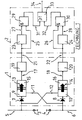
Zeichnung 1.- Prinzipielles Blockschaltbild der Einrichtung
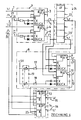
Zeichnung 2.- Signalgeber/Empfänger mit Optokoppler sowie NICHT-Glieder und monostabile Multivibratoren als Entpreller/Pulsformer
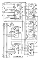
Zeichnung 3.- Signalgeber/Empfänger mit EIN-AUS-Schaltrelais sowie NICHT-Glieder und monostabile Multivibratoren als Entpreller/Pulsformer
Zeichnung 4.- Signalgeber/Empfänger mit EIN-EIN-Schaltrelais sowie NICHT-Glieder als Entpreller/Pulsformer
Zeichnung 5.- Signalgeber/Empfänger mit EIN-EIN-Schaltrelais und NICHT-UND-Gatter als Entpreller/Pulsformer
Zeichnung 6.- Impulswächter und analoger Timer mit UND/NICHT-ODER-Gatter als Steuersignalgeber
Zeichnung 7.- Impulswächter und digitaler Zähler/Timer mit UND/NICHT-ODER-Gatter als Steuersignalgeber
-
Drawing 1. - Basic block diagram of the facility
-
Drawing 2. - Signal generator / receiver with optocoupler as well as non-links and monostable multivibrators as debouncer / pulse shaper
-
Drawing 3. - Signal generator / receiver with ON-OFF switching relay as well as non-elements and monostable multivibrators as debouncing / pulse shapers
-
Drawing 4. - Signal generator / receiver with ON-ON switching relay and non-elements as debouncing / pulse shaper
-
Drawing 5. - Signal generator / receiver with ON-ON switching relay and NAND gate as debouncer / pulse shaper
-
Drawing 6. - Pulse monitor and analog timer with AND / NOT-OR gate as control signal generator
-
Drawing 7. - Pulse monitor and digital counter / timer with AND / NOT-OR gate as control signal generator
Die Blinkgeber der heutigen Blinkanlagen sind mehrheitlich mit elektronisch gesteuerten Schaltrelais ausgestattet. Auch werden noch thermisch gesteuerte sogen. Bimetallschalter angewendet. Erfahrungsgemäss lässt sich, unabhängig von der Wahl des verwendeten Blinkgebers, das sogen. Prellen der Schalterkontakte dieser Blinkgeber nicht vermeiden. Beim Betrieb der Blinkanlage stört dies zwar weiter nicht, für den Betrieb der erfindungsgemässen Einrichtung würde das Prellen dieser Kontakte aber zu unerwünschten Störimpulsen führen.The flasher units of today's turn signal systems are mostly with electronically controlled switching relays fitted. They are also thermally controlled so-called Bimetal switch applied. According to experience can be used regardless of the choice of the used Flasher, the so-called. Bouncing of the switch contacts do not avoid this flasher. When operating the The turn signal system does not interfere with this, for operation the device according to the invention would bounce of these contacts, however, to undesired interference pulses to lead.
Insbesonders im Sinne einer breiten Anwendbarkeit der erfindungsgemässen Einrichtung ist es deswegen notwendig, die durch das Prellen verursachten Störimpulse wirksam zu unterdrücken.Especially in terms of broad applicability it is therefore the device according to the invention necessary, the interference caused by the bouncing suppress effectively.
Deshalb ist den verschiedenen Ausführungsformen der Erfindung gemeinsam, dass die von der rechts- bzw. linksseitigen Stromzuführung der Blinklampen stammenden Spannungsimpulse zuerst einem Signalsender/Signal-empfänger mit nachfolgendem Entpreller/Pulsformer zugeleitet werden, bevor ihre weitere Verarbeitung stattfinden kann.Therefore, the various embodiments of the Invention in common that the legal or left-hand power supply of the flashing lights Voltage pulses first to a signal transmitter / signal receiver with subsequent debouncer / pulse shaper be forwarded before their further processing can take place.
Die Einrichtung (Zeichnung 1) ist in ihren verschiedenen Ausführungsvarianten aus zwei Blöcken (1,2) aufgebaut. The facility (drawing 1) is in their different versions from two blocks (1,2) built up.
Der erste Block (1) erzeugt elektrische Signale beim Auftreten von Blinksignalen in den Stromzuführungen (5,6) von entweder einer rechten (3) oder einer linken (4) Blinklampe, nicht aber bei gleichzeitig auf beiden Seiten des Fahrzeugs auftretenden Blinksignalen (sogen. Warnblinken). Diese Signale werden anschliessend vom Entpreller/Pulsformer (19,20) systemkompatibel normiert, sodass sie bei allen Varianten der Einrichtung am Ausgang des ersten Blocks (1) störungsfrei als komplementäre Signalpaare, jeweils rechtsseitig (21) bzw. linksseitig (22) zugeordnet, zur Verfügung stehen.The first block (1) generates electrical signals when Blinking signals appear in the power supply lines (5,6) from either a right (3) or a left (4) Flashing light, but not on both sides at the same time flashing signals of the vehicle (so-called warning flashes). These signals are then from Debouncer / pulse shaper (19.20) standardized for system compatibility, so that they are at the exit with all variants of the facility of the first block (1) without interference as complementary Signal pairs, each on the right side (21) or left side (22) are assigned.
Der zweite Block (2) überwacht die Stetigkeit der im
ersten Block (1) erzeugten Signale (21,22) sowie die
Gesamtzeitdauer des Blinkens und erzeugt bei Erfüllung
des Kriteriums "Anzahl Blinksignale rechts- oder linksseitig
überschritten" bzw. bei "Blinkdauer rechts- oder
linksseitig überschritten" ein rechts/links-unabhängiges
Steuersignal 34.The second block (2) monitors the continuity of the
first block (1) generated signals (21,22) and
Total duration of blinking and generated when fulfilled
the criterion "number of flashing signals on the right or left side
exceeded "or with" flashing time right or
left side exceeded "a right / left
Der erste Block (1) der Einrichtung (Zeichnung 1) wird nun in seiner Funktionsweise eingehender beschrieben. Er greift den beim rechtsseitigen (linksseitigen) Blinken auftretenden Spannungsanstieg auf der vom Blinkgeber geschalteten Stromzuführung 5 (6) einer rechten (linken) Blinklampe 3 (4) ab und führt ihn über eine Diode 7 (8) und nötigenfalls über einen nicht eingezeichneten Widerstand einem rechtsseitigen (linksseitigen) Signalsender 9 (10) zu. The first block (1) of the device (drawing 1) is now more detailed in its operation described. He attacks the one on the right (left-hand) flashing occurring voltage increase the power supply 5 (6) switched by the flasher unit a right (left) turn signal lamp 3 (4) and guides it via a diode 7 (8) and if necessary not via one drawn resistance a right-hand side (left-hand) signal transmitter 9 (10) to.
Um den Stromkreislauf des rechten bzw. linken Signalsenders 9 (10) zu schliessen sind letztere ausgangsseitig über die Leitung 11 (12) mit der vom Blinkgeber geschalteten Stromzuführung 6 (5) der linksseitigen (rechtsseitigen) Blinklampe 4 (3) verbunden.To the circuit of the right or left Signal transmitters 9 (10) to close are the latter on the output side via line 11 (12) with that of Flasher switched power supply 6 (5) of the left-hand (right-hand) flashing light 4 (3) connected.
Der Signalsender sendet berührungsfrei ein Signal 13
(14) zu einem Signal-Empfänger 15 (16). Dieser Signal-empfänger
erzeugt ein elektrisches Signal 17 (18) welches
im allgemeinen noch mit Störungen überlagert ist. Beide
Signale (17,18) werden in einem nachfolgenden
Entpreller/Pulsformer 19 (20) zu einem störungsfreien,
systemkompatibel normierten und komplementären Signalpaar
21 (22) umgeformt. Diese Ausgangssignale 21 (22) werden
anschliessend von den Schaltungsbauteilen des zweiten
Blocks (2) rechts/links-selektiv weiterverarbeitet.The signal transmitter transmits a
Der zweite Block (2) der Einrichtung (Zeichnung 1) wird nun in seiner Funktionsweise eingehender beschrieben. Er enthält rechts- bzw. linksseitig zugeordnet je eine Impulswächter/Timer-Einheit 23 (24), sowie ein oder mehrere seitenunabhängige UND/ODER- bzw. UND/NICHT-ODER-Gatter zwecks Signalverknüpfung der beim rechtsseitigen bzw. linksseitigen Blinken erzeugten Signale, hier beispielsweise dargestellt durch die beiden UND-Gatter 29 (30) und das ODER-Gatter 33.The second block (2) of the device (drawing 1) is now more detailed in its operation described. It contains right and left sides assigned a pulse monitor / timer unit 23 (24), as well as one or more page-independent AND / OR or AND / NOT-OR gate for the purpose of signal linking of the at flashing on the right or left side Signals, represented here by the two, for example AND gate 29 (30) and OR gate 33.
Die Impulswächter/Timer-Einheit 23 (24) überprüft
das stetige Eintreffen der beim Betrieb der Blinkanlage
in der Einrichtung erzeugten Signale. Das Ausschalten der
Blinkanlage bzw. der Seitenwechsel von rechts auf links
oder umgekehrt unterbricht die stetige Impulsfolge worauf
der Impulswächter den Timer zurücksetzt. Der Timer
erzeugt, vorausgesetzt dass er nicht vorher vom Impulswächter
zurückgesetzt wurde, nach einer digital
voreinstellbaren Anzahl von Blinksignalen bzw. nach einer
analog voreinstellbaren Blinkdauer, ein Ausgangssignal 27
(28). Die von der Impulswächter/Timer-Einheit 23 (24)
abgegebenen Signale 27 (28) werden, zusammen mit den vom
Entpreller/Pulsformer 19 (20) erzeugten Ausgangssignalen
21 (22) den Signaleingängen der UND-Gatter 29 (30) über
die Leitungen 25 (26) zugeführt. Die jeweiligen
Ausgangssignale der UND-Gatter 29 (30) werden über die
Leitungen 31 (32) den Signaleingängen des ODER- bzw.
NICHT-ODER-Gatters 33 zugeführt wobei am Signalausgang
dieses Gatters ein vielseitig verwendbares, periodisch im
Rhythmus der von der Blinkanlage abgegebenen Blinksignale
pulsierendes Steuersignal 34 entsteht.Check the pulse monitor / timer unit 23 (24)
the constant arrival of the flashing system
signals generated in the device. Turning off the
Turn signal or changing sides from right to left
or vice versa, the continuous pulse sequence interrupts what
the pulse monitor resets the timer. The timer
generated, provided that it has not previously been generated by the pulse monitor
was reset after a digital
preset number of flashing signals or after one
flashing duration that can be preset analogously, an output signal 27
(28). From the pulse monitor / timer unit 23 (24)
emitted signals 27 (28), together with the from
Debouncer / pulse shaper 19 (20) generated output signals
21 (22) the signal inputs of the AND gates 29 (30) over
the lines 25 (26) fed. The respective
Output signals of the AND gates 29 (30) are via the
Lines 31 (32) the signal inputs of the OR or
NOR gate 33 supplied being at the signal output
this gate is a versatile, periodic in
Rhythm of the flashing signals emitted by the flashing system
pulsating
Dieses Steuersignal kann z.B. zur Ansteuerung eines Summers verwendet werden, welcher den Fahrzeuglenker auf den fortwährenden Betrieb der Blinkanlage aufmerksam macht. Falls die vorhandene Blinkanlage dies schaltungstechnisch zulässt, kann die erfindungsgemässe Einrichtung die Blinkanlage auch automatisch abschalten und dabei ggf. gleichzeitig den Fahrzeuglenker akustisch warnen. This control signal can e.g. to control a Summers are used, which the vehicle driver on the continuous operation of the turn signal system carefully makes. If the existing turn signal system does this in terms of circuitry allows the device according to the invention also turn off the turn signal automatically while doing so if necessary, give the vehicle driver an acoustic warning at the same time.
Die Funktionsweise der vorliegenden Erfindung wird nun eingehender erklärt unter Einbezug von integrierten Elektronikbausteinen aus einer unter dem Namen Transistor-Transistor-Logik (TTL) allgemein bekannten und vielseitig angewandten Technik, ohne damit jedoch die Verwendung ähnlicher Verfahren zur Verwirklichung der erfindungsgemässen Einrichtung auszuschliessen. In diesem Sinne werden im nachfolgenden Typenbezeichnungen integrierter TTL-Schaltkreise verwendet, welche stellvertretend für die verwendeten Funktionen, wie z.B. von Asynchronzähler, monostabile Multivibratoren, logische Gatter usw. stehen.The operation of the present invention will now explained in more detail with the inclusion of integrated Electronic components from one under the name Transistor-transistor logic (TTL) well known and versatile applied technology, but without the Using similar procedures to achieve the Exclude device according to the invention. In this The following are designations of meaning integrated TTL circuits used, which representative for the functions used, e.g. from Asynchronous counters, monostable multivibrators, logical Gates etc. stand.
Zuerst werden die vier verschiedenen Ausführungsformen für die Verwirklichung vom ersten Block (1) der Einrichtung (Zeichnung 1) dargelegt.First, the four different embodiments for the realization of the first block (1) of the Facility (drawing 1) outlined.
Der nachfolgend beschriebenen ersten und zweiten Ausführungsform des Signalsenders/Signalempfängers bzw. Entpreller/Pulsformers der Einrichtung ist gemeinsam, dass ein nicht-retriggerbarer monostabiler Multivibrator (sogen. nicht-retriggerbares Monoflop) mit geeignet gewählter und durch Beschaltung mit externen Beschaltungselementen (Widerstände, Kondenstoren, Dioden) bewerkstelligter Verweilzeit in den instabilen Zustand es den Störimpulsen verunmöglicht, die Schaltung zu beeinflussen, sobald der ersteintreffende Impuls das Monoflop aus seinem stabilen Zustand in den instabilen Zustand versetzt hat. Da das Monoflop bei geeignet gewählter Verweilzeit vor dem nächsten Blinksignal wieder vom instabilen Zustand in den stabilen Zustand zurückfällt, ist die Verarbeitung nachfolgender Signalimpulse uneingeschränkt gewährleistet.The first and second described below Embodiment of the signal transmitter / signal receiver or The device's debouncer / pulse shaper is common, that a non-retriggerable monostable multivibrator (so-called non-retriggerable monoflop) selected and by wiring with external Wiring elements (resistors, capacitors, diodes) accomplished residence time in the unstable state it the glitches make the circuit impossible influence as soon as the first impulse Monoflop from its stable state to the unstable State. Because the monoflop is suitable at selected dwell time before the next flashing signal falls back from the unstable state to the stable state, is the processing of subsequent signal pulses fully guaranteed.
Die Vorschaltung eines NICHT-Glieds mit Schmitt-Trigger-Funktion bzw. zweier solcher NICHT-Glieder in Serie zur Ansteuerung zweier oder mehr Signaleingängen des nicht-retriggerbaren Monoflops bewirkt aufgrund der Phasenverschiebung der Störimpulse und des sogen. Totbandes der Schmitt-Trigger eine weitere Sicherheit gegen Störimpulse.The upstream connection of a NOT gate with Schmitt trigger function or two such NOT terms in Series for controlling two or more signal inputs of the non-retriggerable monoflop due to the Phase shift of the interference pulses and the so-called. Dead band of the Schmitt trigger another security against interference.
Bei der ersten Ausführungsform (Zeichnung 2) werden Optokoppler (9,10) als Signalsender/Empfänger benutzt. Als Entpreller/Pulsformer werden nicht-retriggerbare monostabile Multivibratoren (33,34) wie z.B. TTL-Type 74221 mit im Verhältnis zur Periodizität der Blinksignale kurzer Verweilzeit in den instabilen Zustand eingesetzt welche von NICHT-Glieder mit Schmitt-Trigger-Funktion (15,16,19,20) wie z.B. TTL Type 7414 angesteuert werden.In the first embodiment (drawing 2) Optocoupler (9,10) used as a signal transmitter / receiver. As a debouncer / pulse shaper are non-retriggerable monostable multivibrators (33,34) such as TTL type 74221 with in relation to the periodicity of the flashing signals short dwell time used in the unstable state which of NON gates with Schmitt trigger function (15,16,19,20) such as TTL Type 7414 can be controlled.
Beim rechtsseitigen (linksseitigen) Blinken der Blinklampe 1 (2) erzeugt der an der Stromzuführung 3 (4) der Blinklampe auftretende Spannungsanstieg einen durch den Widerstand 5 (6) begrenzten und durch die Diode 7 (8) rechts/links-selektiv zugeordneten Strom durch die jeweilige Licht Emittierende Diode (LED) des Optokopplers 9 (10). Dabei wird der hier als Beispiel eingezeichnete npn-Transistor des Optokopplers vom LED aktiviert. Die Verwendung anderer Optokoppler-Typen, wie beispielsweise mit pnp-Transistoren statt npn-Transistoren oder mit als Darlington-Schaltungen bekannten Transistor-Anordnungen ist damit aber keineswegs ausgeschlossen. Bei Aktivierung des Transistors einer der Optokoppler 9 (10) sinkt die Spannung am vorher durch den Widerstand 11 (12) auf einem Logisch-HIGH von beispielsweise 5 Volt gehaltenen Signaleingang 13 (14) des NICHT-Glieds 16 (20) auf einem Logisch-LOW von beispielsweise 0.2 Volt ab, was den Ausgang 21 (22) des NICHT-Glieds 16 (20) auf Logisch-HIGH einstellt. Dadurch werden die sogen. Zustands-Eingänge 27 (28) und 31 (32) sowie der Rückstelleingang "R" des Monoflops 33 (34) ebenfalls auf Logisch-HIGH gelegt. Gleichzeitig wird das Logisch-HIGH-Ausgangssignal 21 (22) des NICHT-Glieds 16 (20) dem Signaleingang 23 (24) des NICHT-Glieds 15 (19) zugeführt und von diesem an seinem Ausgang 25 (26) nach einer für das NICHT-Glied typischen Verzögerungszeit von beispielsweise 15 nanoSekunden in ein Logisch-LOW umgewandelt. Die abfallende Signalflanke dieser Umstellung erreicht den flankengesteuerten dynamischen Eingang 29 (30) des bereits an den Zustands-Eingängen 27 (28) bzw. 31 (32) vorbereiteten UND-Gatters des Monoflops 33 (34) um diese 15 nanoSekunden verzögert und versetzt dabei das Monoflop in den instabilen Zustand. Dabei ist das Monoflop gegenüber dem am jeweiligen Rückstelleingang "R" anliegenden Logisch-HIGH-Signal indifferent. When the right side (left side) flashes Flashing lamp 1 (2) generates the on the power supply 3 (4) of the flashing lamp occurring voltage rise through limited the resistor 5 (6) and by the diode 7 (8) right / left-selectively assigned current through the respective light-emitting diode (LED) of the optocoupler 9 (10). The example shown here is shown here npn transistor of the optocoupler activated by the LED. The Use of other types of optocouplers, such as with pnp transistors instead of npn transistors or with as Darlington circuits known transistor arrangements is by no means excluded. When activated of the transistor one of the optocouplers 9 (10) drops Voltage on previously through resistor 11 (12) on one Logically HIGH of 5 volts, for example Signal input 13 (14) of NOT gate 16 (20) on one Logical-LOW from 0.2 volts, for example, what the Output 21 (22) of NOT gate 16 (20) to logic HIGH sets. As a result, the so-called. State inputs 27 (28) and 31 (32) and the reset input "R" of the Monoflops 33 (34) also set to logic HIGH. At the same time, the logic HIGH output signal 21 (22) of the NOT gate 16 (20) the signal input 23 (24) of the NOT link 15 (19) supplied and by this at his Output 25 (26) after a typical for the NON-link Delay time of, for example, 15 nano seconds in a logical LOW converted. The falling signal edge this change reached the edge-controlled dynamic input 29 (30) of the already at the state inputs 27 (28) or 31 (32) prepared AND gate of the monoflop 33 (34) is delayed by these 15 nano-seconds and thereby puts the monoflop in the unstable Status. The monoflop is opposite to the logic HIGH signal present at the respective reset input "R" indifferent.
Durch geeignete Wahl der externen Beschaltungselemente (Widerstände, Kondensatoren, Dioden) der CX bzw. RX/CX-Eingänge der Monoflops wird eine Verweilzeit in den instabilen Zustand von beispielsweise 0.1 Sekunden Dauer vorgegeben, welche Zeit einerseits genügend lang ist um die Prellphase der Relaiskontakte völlig auszublenden aber andererseits kurz genug, um das Monoflop wieder rechtzeitig vor dem vom nächsten Blinksignal verursachten Signal in den stabilen Zustand zurückkehren zu lassen.By suitable choice of the external wiring elements (Resistors, capacitors, diodes) of the CX or RX / CX inputs of the monoflops will have a residence time in the unstable state of 0.1 seconds, for example given which time is long enough on the one hand completely hide the bounce phase of the relay contacts but on the other hand short enough to get the monoflop back in time before the one caused by the next blinking signal Signal to return to the stable state.
Die Ausgänge der Monoflops 33 (34) dieser Schaltung liefern, jeweils rechts- bzw. linksseitig zugeordnet, systemkompatible und paarweise komplementäre Signale (35,36 bzw. 37,38).The outputs of the monoflops 33 (34) of this circuit deliver, assigned on the right or left side, system compatible and pairwise complementary signals (35.36 and 37.38).
Bei der zweiten Ausführungsform (Zeichnung 3) werden Schaltrelais mit EIN-AUS-Funktion 7 (8) als Signalsender/Empfänger benutzt. Als Entpreller/Pulsformer werden NICHT-Glieder mit Schmitt-Trigger-Funktion (13,14,17,18) wie z.B. TTL Type 7414 eingesetzt welche nicht-retriggerbare monostabile Multivibratoren (33,34) wie z.B. vom TTL-Type 74221 mit im Verhältnis zur Periodizität der Blinksignale kurzer Verweilzeit in den instabilen Zustand ansteuern.In the second embodiment (drawing 3) Switching relay with ON-OFF function 7 (8) as a signal transmitter / receiver used. As debouncer / pulse shaper become NOT links with a Schmitt trigger function (13,14,17,18) such as TTL Type 7414 used which non-retriggerable monostable multivibrators (33,34) such as. of TTL type 74221 with in relation to Periodicity of the flashing signals in the short dwell time Control unstable condition.
Beim rechtsseitigen (linksseitigen) Blinken der Blinklampe 1 (2) erzeugt der an der Stromzuführung der Blinklampe 3 (4) auftretende Spannungsanstieg mit Hilfe der Diode 5 (6) einen rechts/links-selektiv zugeordneten Strom durch das EIN-AUS-Schaltrelais 7 (8). Bei der Aktivierung eines dieser Schaltrelais sinkt die Spannung am vorher durch den Widerstand 9 (10) beispielsweise auf einem Logisch-HIGH von beispielsweise 5 Volt gehaltenen Signaleingang 11 (12) des NICHT-Glieds 14 (18) auf einem Logisch-LOW von 0 Volt ab, was den Ausgang 21 (22) des NICHT-Glieds 14 (18) auf Logisch-HIGH einstellt.When the right side (left side) flashes Flashing lamp 1 (2) generates the on the power supply of Flashing lamp 3 (4) occurring voltage increase with the help the diode 5 (6) is assigned a right / left selectively Current through the ON-OFF switching relay 7 (8). In the Activation of one of these switching relays reduces the voltage on previously through resistor 9 (10), for example a logic HIGH of, for example, 5 volts Signal input 11 (12) of the NOT element 14 (18) on one Logical LOW from 0 volts, which is the output 21 (22) of the NOT gate 14 (18) set to logic HIGH.
Damit ist die gleiche Ausgangslage wie bei der vorgängigen Beschreibung der von Optokopplern angesteuerten Entpreller/Pulsformern gegeben, sodass auf eine Wiederholung verzichtet werden kann.This is the same starting point as for the previous description of that of optocouplers controlled debouncer / pulse shaper given, so on a repetition can be omitted.
Die Ausgänge dieser Schaltung liefern ebenfalls, jeweils rechts- bzw. linksseitig zugeordnet, systemkompatible und paarweise komplementäre Signale.The outputs of this circuit also deliver each assigned to the right or left side, system compatible and pairwise complementary signals.
Die dritte Ausführungsform (Zeichnung 4) des Signalsender/Signalempfängers bzw. Entpreller/Pulsformers der Einrichtung verwendet für den Signal sender/Empfänger Schaltrelais mit einer EIN-EIN-Schaltfunktion (7,8). Als Entpreller/Pulsformer werden jeweils paarweise zwei NICHT-Glieder (17,18 bzw. 19,20) wie z.B. vom TTL-Type 7404 oder 7414 pro Schaltrelais eingesetzt.The third embodiment (drawing 4) of Signal transmitter / signal receiver or debouncer / pulse shaper the device used for the signal transmitter / receiver Switching relay with an ON-ON switching function (7,8). As Debouncers / pulse shapers become two in pairs NOT gates (17.18 or 19.20) such as of the TTL type 7404 or 7414 used per switching relay.
Beim rechtsseitigen (linksseitigen) Blinken der Blinklampe 1 (2) erzeugt der an der Stromzuführung der Blinklampe 3 (4) auftretende Spannungsanstieg einen mit Hilfe der Diode 5 (6) rechts/links-selektiv zugeordneten Strom durch das EIN-EIN-Schaltrelais 7 (8). Bei der Aktivierung eines dieser EIN-EIN-Schaltrelais werden die Signaleingänge der zugehörigen NICHT-Glieder-Paare (13,14 bzw. 15,16) unter Mitwirkung der vier Widerstände (9,10 bzw. 11,12) von einem Logisch-LOW von 0 Volt auf einem Logisch-HIGH von beispielsweise 5 Volt bzw. umgekehrt, umgepolt. Die Rückführung des invertierten Ausgangssignals eines NICHT-Glieds der NICHT-Glieder-Paare (17,18 bzw. 19,20) über die Leitungen (21,22 bzw. 23,24) zum Signaleingang des jeweils anderen NICHT-Glieds dieser Paare verleiht dieser Schaltung ein bistabiles Verhalten welches dazu führt, dass ein Prellen der EIN-EIN-Schaltrelais und/oder der Blinkgeberkontakte ohne Auswirkung in der Form von Störimpulsen bleibt.When the right side (left side) flashes Flashing lamp 1 (2) generates the on the power supply of Flashing lamp 3 (4) occurring voltage increase with With the help of diode 5 (6) selectively assigned to the right / left Current through the ON-ON switching relay 7 (8). In the Activation of one of these ON-ON switching relays are the Signal inputs of the associated non-link pairs (13, 14 or 15.16) with the participation of the four resistors (9.10 or 11.12) from a logic LOW of 0 volts to one Logical-HIGH of 5 volts or vice versa, reversed polarity. The feedback of the inverted output signal a NON-link of the NON-link pairs (17.18 or 19.20) via the lines (21.22 or 23.24) to Signal input of each other's NOT element Couples give this circuit a bistable behavior which leads to bouncing of the ON-ON switching relay and / or the flasher switch contacts without Impact remains in the form of glitches.
Die Ausgänge dieser Schaltung liefern, jeweils rechts- bzw. linksseitig zugeordnet, systemkompatible und paarweise komplementäre Signale (25,26 bzw. 27,28).The outputs of this circuit deliver, respectively assigned on the right or left side, system compatible and complementary signals in pairs (25.26 and 27.28).
Die Verwendung von NICHT-Glieder hat bei der handelsüblichen Ausgestaltung der als Beispiel erwähnten TTL-Bausteinen den Vorteil, dass von den sechs in einem solchen Baustein vorhandenen NICHT-Glieder nur deren vier für die Entprellung/Pulsformung benötigt werden, sodass im Falle der Verwendung analoger Timer die zwei nicht benutzten NICHT-Glieder als Verzögerer für den Eingangsimpuls am flankengesteuerten dynamischen Eingang der Monoflops dieser analogen Timer kostensparend verwendet werden können. The use of NOT links has been used in the commercial design of the mentioned as an example TTL modules have the advantage that of the six in one Only four elements of such a block exist for debouncing / pulse shaping, so that in the case of using analog timers the two will not used NOT links as retarders for the Input pulse at the edge-controlled dynamic input the monoflops of these analog timers save money can be used.
Die vierte Ausführungsform (Zeichnung 5) des Signalgeber/Signalempfängers bzw. Entpreller/Pulsformers der Einrichtung benutzt für den Signalsender/Empfänger ebenfalls Schaltrelais (7,8) mit EIN-EIN-Schaltfunktion. Als Entpreller/Pulsformer werden jeweils paarweise zwei NICHT-UND-Gatter (17,18 bzw. 19,20) wie z.B. vom TTL-Type 7400 pro Schaltrelais eingesetzt.The fourth embodiment (drawing 5) of Signal generator / signal receiver or debouncer / pulse shaper the device used for the signal transmitter / receiver also switching relay (7,8) with ON-ON switching function. As debouncer / pulse shaper, there are two in pairs NAND gates (17, 18 and 19, 20) such as of the TTL type 7400 used per switching relay.
Beim rechtsseitigen (linksseitigen) Blinken der Blinklampe 1 (2) erzeugt der an der Stromzuführung der Blinklampe 3 (4) auftretende Spannungsanstieg mit Hilfe der Diode 5 (6) einen rechts/links-selektiv zugeordneten Strom durch das EIN-EIN-Schaltrelais 7 (8). Durch die Aktivierung eines der beiden EIN-EIN-Schaltrelais (7,8) werden die Signaleingänge der zugehörigen NICHT-UND-Gatterpaare (13,14 bzw. 15,16) unter Mitwirkung der vier Widerstände (9,10 bzw. 11,12) von einem Logisch-LOW von 0 Volt auf einem Logisch-HIGH von beispielsweise 5 Volt bzw. umgekehrt, umgepolt. Die Rückführung des invertierten Ausgangssignals eines NICHT-UND-Gatters der NICHT-UND-Gatterpaare (17,18 bzw. 19,20) über die Leitungen (21,22 bzw. 23,24) zum Signaleingang des jeweils anderen NICHT-UND-Gatters dieser Paare verleiht dieser Schaltung ein bistabiles Verhalten welches dazu führt, dass ein Prellen der EIN-EIN-Schaltrelais und/oder der Blinkgeberkontakte ohne Auswirkung in der Form von Störimpulsen bleibt. When the right side (left side) flashes Flashing lamp 1 (2) generates the on the power supply of Flashing lamp 3 (4) occurring voltage increase with the help the diode 5 (6) is assigned a right / left selectively Current through the ON-ON switching relay 7 (8). Through the Activation of one of the two ON-ON switching relays (7,8) become the signal inputs of the associated NAND gate pairs (13.14 and 15.16) with the participation of the four Resistors (9,10 and 11,12) from a logic LOW of 0 Volts on a logic HIGH of 5 volts, for example or vice versa, reversed the polarity. The return of the inverted output signal of a NAND gate NAND gate pairs (17, 18 and 19, 20) over the Lines (21, 22 and 23, 24) to the signal input of the each other gives other NAND gates of these pairs this circuit has a bistable behavior causes a bouncing of the ON-ON switching relay and / or the flasher contacts without any effect in the form of Interference pulses remain.
Die Ausgänge dieser Schaltung liefern, jeweils rechts- bzw. linksseitig zugeordnet, systemkompatible und paarweise komplementäre (25,26 bzw. 27,28) Signale.The outputs of this circuit deliver, respectively assigned on the right or left side, system compatible and complementary (25.26 and 27.28) signals in pairs.
Da die handelsübliche Ausführung der erwähnten TTL-Bausteine nur über vier NICHT-UND-Gatter verfügt, sind NICHT-UND-Gatter nur dann vorteilhaft einzusetzen, wenn keine NICHT-Glieder für die nachfolgenden Impulswächter/Timer gebraucht werden, d.h. bei der Verwendung von digitalen Timern.Because the commercial version of the TTL modules mentioned only has four NAND gates Use NAND gates only if no NOT elements for the subsequent pulse monitors / timers are needed, i.e. when using of digital timers.
Die Ausgangssignale aller vier oben angeführten Schaltungen welche (Zeichnung 1) am Ausgang vom ersten Block (1) der Einrichtung, unabhängig von der jeweils gewählten Schaltungsanordnung, rechts-/links-selektiv zugeordnet und systemkompatibel als komplementäre Signalpaare, stellvertretend mit (21,22) bezeichnet zur Verfügung stehen, werden im zweiten Block (2) einem als Impulswächter dienenden Monoflop sowie einem die Verzögerungszeit digital bzw. analog bestimmenden Timer zugeführt.The output signals of all four listed above Circuits which (drawing 1) at the output from the first Block (1) of the establishment, regardless of each selected circuit arrangement, right / left selective assigned and system compatible as complementary Signal pairs, designated as (21,22) for Are available, are in the second block (2) as Pulse monitor serving monoflop and a Delay time digital or analog determining timer fed.
Es wird nun zuerst (Zeichnung 6) die Ausgestaltung des Impulswächter/Timers mit einem analogen Timer, zusammen mit dem das rechts/links-unabhängige Steuersignal erzeugende Verknüpfungsglied, eingehender beschrieben. It is now first (drawing 6) the design the pulse monitor / timer with an analog timer, along with that the right / left independent Control signal generating logic element, more detailed described.
Die rechtsseitig (linksseitig) zugeordneten
Monoflops 3 (4) des Impulswächters 7 sind retriggerbar
(z.B. TTL-Type 74423) und haben beispielsweise eine
Verweilzeit in den instabilen Zustand von 1.2 Sekunden,
welche Zeit prinzipiell geringfügig grösser zu sein hat
als die verkehrsrechtlich zulässige grösste Periode der
Blinkanlage. Diese Zeitdauer wird in der allgemein
üblichen Weise durch die externen Beschaltungselemente
(Widerstände, Kondensatoren, Dioden) dieser Monoflops
vorgegeben. Das rechtsseitig (linksseitig) zugeordnete
Monoflop 3 (4), dessen zustandsabhängiger Signaleingang,
ebenso wie der Rückstelleingang "R" auf einem Logisch-HIGH
von beispielsweise 5 Volt gehalten werden, verweilt
nur so lange unterbruchslos in seiner instabilen Lage als
die durch die Blinksignale erzeugten Signale 1 (2) stetig
und innerhalb der Zeitspanne des instabilen Zustandes
kommen. Beim Ausbleiben der Signale 1 (2), wie z.B. beim
Abschalten der Blinkanlage oder Umschalten der
Blinkanlage auf die andere Seite des Fahrzeugs, fällt das
jeweilige Monoflop in den stabilen Zustand zurück.
Dadurch ermöglicht das Monoflop die Ueberwachung der
Stetigkeit des Betriebs der Blinkanlage. Die Ausgangssignale
(5,6) der Monoflops (3,4) steuern den nachfolgend
beschriebenen, die Verzögerungszeit analog bestimmenden
Timer (8).The right side (left side) assigned
Monoflops 3 (4) of the
Dieser analoge Timer besteht zur Hauptsache aus zwei
rechtsseitig (linksseitig) zugeordneten Monoflops 9 (10)
wie z.B. die des TTL-Bausteins 74423. Diese Monoflops
müssen aufgrund ihrer zulässigen externen Beschaltung mit
Widerständen, Kondensatoren und Dioden in der Lage sein,
eine genügend grosse Verweilzeit in den instabilen
Zustand von z.B. 30 Sekunden zu garantieren. Die analoge
Einstellung dieser Verweilzeit kann beispielsweise
mittels eines sogen. Tandem-Potentiometers (19), welches
als externes Beschaltungselement der RX-Eingänge die
Verweilzeit des Timers (8) in den instabilen Zustand
beeinflusst, durchgeführt werden, wobei mittels
Vorwiderständen (17,18) eine minimale Verzögerungszeit
fest voreingestellt werden kann. In einer einfacheren
Ausführungsform dieses analogen Timers (8) können statt
des Tandem-Potentiometers (19) auch Festwiderstände, ggf.
über Lötbrücken oder dgl. wählbar, verwendet werden.This analog timer mainly consists of two
monoflops 9 (10) assigned on the right-hand side (left-hand side)
such as. that of the TTL block 74423. These monoflops
due to their permissible external wiring
Resistors, capacitors and diodes to be able
a sufficiently large dwell time in the unstable
State of
Das rechtsseitige (linksseitige) Ausgangssignal 5 (6) des
Impulswächters wird unverzögert dem zustandsabhängigen
Signaleingang und dem Rückstelleingang "R" und, jeweils
über ein NICHT-Glied des NICHT-Bausteins 24 verzögert,
als Signalflanke dem flankengesteuerten dynamischen
Signaleingang des Monoflops 9 (10) zugeführt. Diese
Anordnung bewirkt, das die Signalflanke der Signale 5 (6)
um die für das jeweilig verwendete NICHT-Glied 22 (23)
typische Signallaufzeit von beispielsweise 15
nanoSekunden später und in negierter Form am dynamischen
Signaleingang des Monoflops 9 (10) eintrifft als am
zustandsabhängigen Signaleingang oder am flankengesteuerten
Rückstelleingang des Timer-Monoflops (24),
wodurch dessen sichere Umsteuerung in den instabilen
Zustand gewährleistet ist.The right-hand (left-hand) output signal 5 (6) of the
Pulse monitor is instantaneous to the state-dependent
Signal input and the reset input "R" and, each
delayed via a NOT element of the
Es ist dabei vorteilhaft aber nicht zwingend notwendig, für diese NICHT-Glieder 22 (23) die nicht für den Entpreller/Pulsformer (Zeichnung 4) benötigten NICHT-Glieder (29,30) des beispielsweise erwähnten TTL-Bausteins 7414 kostensparend einzusetzen.It is advantageous but not mandatory necessary for these NOT-links 22 (23) which are not for the debouncer / pulse shaper (drawing 4) requires NOT links (29,30) of the TTL module mentioned for example 7414 to save costs.
Sobald die vorgegebene Verweilzeit in den instabilen Zustand des jeweiligen Timer-Monoflops 9 (10) verstrichen ist, entsteht am Signalausgang 11 (12) ein auf Logisch-HIGH gehendes Signal, welches den Signaleingängen eines oder beider UND-Gatter eines Dual-UND/NICHT-ODER-Gatters (25), wie z.B. TTL-Type 7451, zugeführt wird. Die Verknüpfung mit den ebenfalls rechts-/linksseitig zugeordneten und gegenüber den Signalimpulsen 1 (2) komplementären Signalimpulsen 21 (20) vom Entpreller/Pulsformer erzeugt an den Ausgängen des jeweiligen Dual-UND/NICHT-ODER-Gatters (13,14) ein oder mehrere rechts/links-unabhängige Steuersignale (15 bzw. 16). Mit diesen Steuersignalen kann bei geeigneter Beschaltung beispielsweise ein Warnsignal erzeugt werden kann, welches den Fahrzeuglenker darauf aufmerksam macht, dass die Blinkanlage noch in Betrieb ist. Auch kann, die entsprechende Eignung der Blinkanlage vorausgesetzt, letztere, ggf. unter Abgabe eines Warnsignals, ausgeschaltet werden. As soon as the specified dwell time in the unstable State of the respective timer monoflop 9 (10) elapsed is at logic output HIGH at signal output 11 (12) outgoing signal which corresponds to the signal inputs of a or both AND gates of a dual AND / NOT OR gate (25), e.g. TTL type 7451. The Link with the right / left side assigned and compared to the signal pulses 1 (2) complementary signal pulses 21 (20) from Debouncer / pulse shaper generated at the outputs of the respective dual AND / NOT OR gate (13, 14) one or several right / left independent control signals (15 or 16). With these control signals, when appropriate Circuitry, for example, a warning signal can be generated can, which draws the driver's attention to it, that the turn signal system is still in operation. Also can that appropriate suitability of the turn signal system, the latter, possibly with a warning signal, turned off.
Es wird nun die digitale Ausgestaltung des Impulswächter/Timers eingehender dargelegt (Zeichnung 7), wobei auf die bei der analogen Ausgestaltung bereits vorgehend stattgefundenen Beschreibung der Eigenschaften des Impulswächters sowie des UND/NICHT-ODER-Gatters Bezug genommen wird.It is now the digital design of the Pulse monitors / timers detailed (drawing 7), with the already in the analog design previous description of the properties of the pulse monitor and the AND / NOT-OR gate reference is taken.
In dieser digitalen Variante der Einrichtung werden die rechts-/linksseitig zugeordneten, entprellten und systemkompatibel normierten Signale 1 (2) des Entpreller/Pulsformers sowohl den Monoflops 3 (4) des Impulswächters (7) als auch den Zähleingängen eines rechts- bzw. linksseitig zugeordneten und vorzugsweise aus jeweils einem Dual-4-Bit-Asynchronzähler wie z.B. vom TTL-Type 74393 aufgebauten und wahlweise als 6-,7- oder 8-Bit-Zähler geschalteten Asynchronzählers (8,9) zugeführt. Weiters werden diese Signale oder die ebenfalls vom Entpreller/Pulsformer bereitgestellten und mit letzteren komplementären Signale den Signaleingängen des UND/NICHT-ODER-Gatters (19) zugeführt. Die Funktion des Impulswächters ist identisch mit der Funktion des bereits bei der Ausgestaltung des Impulswächter/Timers mit analogem Timer beschriebenen Impulswächters, sodass hier auf eine vollständige Wiederholung verzichtet werden kann. Desgleichen gilt für die Funktion des UND/NICHT-ODER-Gatters. In this digital variant of the facility the right / left assigned, debounced and system-compatible standardized signals 1 (2) of the Debouncer / pulse shaper both the monoflops 3 (4) of the Pulse monitor (7) as well as the counter inputs assigned on the right or left side and preferably each of a dual 4-bit asynchronous counter such as from TTL-Type 74393 assembled and optionally as 6-, 7- or 8-bit counter switched asynchronous counter (8.9) fed. Furthermore, these signals or the also provided by the debouncer / pulse shaper and with the latter complementary signals the signal inputs of the AND / NOT-OR gate (19) supplied. The function the pulse monitor is identical to the function of the already in the design of the pulse monitor / timer pulse monitor described with analog timer, so a complete repetition can be dispensed with here can. The same applies to the function of the AND / NOT-OR gate.
Das rechts-/linksseitig zugeordnete Ausgangssignal 5
(6) der Monoflops 3 (4) des Impulswächters (7), welches
bei stetigem Blinken der Blinkanlage ununterbrochen einen
Logisch-LOW-Pegel aufweist, wird an die Rückstelleingänge
(CT=0) der Asynchronzähler (10,11 bzw. 12,13) gelegt, was
das Zählen der an die Zähleingänge der Asynchronzähler 10
(12) eintreffenden und durch die Blinksignale verursachten
Impulse ermöglicht. Das Resultat dieser Zählvorgänge
erscheint binär kodiert an den Zählausgängen (CT 0..3)
der Asynchronzähler 10(12). Einer dieser Zählausgänge (CT
0..3) ist jeweils mit dem Zähleingang des ihm
nachgeschalteten Asynchronzählers 11 (13) verbunden. Die
Auswahl des Zählausganges (CT 0..3) bestimmt dabei sowohl
die maximal einstellbare Impulszahl als auch die Schrittgrösse
dieser Einstellung. Die Logikpegel der vier
Zählausgänge (CT 0..3) der Asynchronzähler 11 (13) werden
mit Hilfe von als Komparatoren (Vergleicher) bekannten
elektronischen Bausteinen, wie z.B. vom TTL-Type 7485,
mit einer digital in der Form von Logikpegeln voreinstellbaren
Impulszahl verglichen. Dazu werden diese
Zählausgänge (CT 0..3) mit den Istwert-Eingängen (P 0..3)
der Komparatoren 16 (17) verbunden. Die Uebertragungseingänge
"<" bzw. "=" werden an Logisch-LOW, der Uebertragungseingang
">" an Logisch-HIGH gelegt. Der
Komparator vergleicht die an seinem Istwert-Vergleichseingang
(P 0..3) anliegenden und vom Asynchronzähler 11
(13) vorgegebenen Logikpegel (CT 0..3) mit den von einem
4-Bit-Kodierschalter (18) und den ihm zugeordneten vier
Widerständen (20 bis 23) erzeugten und am Sollwert-Eingang
des Komparators (Q 0..3) anliegenden Logikpegeln.
Sobald einer dieser rechts- bzw. linksseitig zugeordneten
Komparatoren 16 (17) das Ueberschreiten der vorgegebenen
Impulszahl feststellt, geht der Ausgang (P>Q) der
Komparatoren auf Logisch-HIGH. Mit diesem Signal können
die bereits bei der Ausgestaltung des Impulswächter/Timers
mit einem analogen Timer näher
beschriebenen UND/NICHT-ODER-Gatter (19) angesteuert
werden. Bei Beendigung des Blinkens stellt der Impulswächter
die Asynchronzähler (10,11 bzw. 12,13) über die
jeweiligen Rückstelleingänge (CT=0) zurück.The
Diese Anordnung ermöglicht aufgrund der frei
wählbaren Verbindung der Signalausgänge (CT 0 bzw. CT 1
bzw. CT 2 oder CT 3) der Asynchronzähler 10 (12) mit den
Zähleingangen der nachgeschalteten Asynchronzähler 11
(13) eine Auswahl aus verschieden grossen diskreten
Einstellschritten, wie folgende Tabelle zeigt:
Wie die praktische Erfahrung zeigt, ist eine Einstellung der maximalen Anzahl Blinksignale unterhalb 30 im allgemeinen wenig sinnvoll. Dadurch fällt ein Abgriff am Signalausgang (CT 0) aus rein praktischen Gründen ausser Betracht. Auch hat sich in der Praxis gezeigt, dass eine Abstufung in Vierer- oder Achter-Schritten am sinnvollsten ist.As practical experience shows, one is Setting the maximum number of flashes below 30 generally makes little sense. This makes one think Tap at the signal output (CT 0) from purely practical Reasons out of consideration. Has also been put into practice shown that a gradation in steps of four or eight makes the most sense.
Claims (22)
Das Ausgangssignal des zweiten Bits des ersten 4-Bit-Asynchronzählers ist dabei an den Signaleingang des zweiten 4-Bit-Asynchronzählers gelegt.
Die HIGH/LOW-Signalpegel der vier Signalausgänge des zweiten 4-Bit-Asynchronzählers werden vom 4-Bit-Komparator verglichen mit den mittels 4-Bit-Kodierschalter und der diesem zugeordneten Widerstände voreinstellbaren logischen HIGH/LOW-Signalpegeln, was eine Einstellung der Begrenzung der Anzahl Blinksignale in diskreten Vierer-Stufen ermöglicht, wobei der 4-Bit-Komparator beim Ueberschreiten der voreingestellten Anzahl Blinksignale ein Signal erzeugt, das geeignet ist, durch logische Verknüpfung mit dem von den Entpreller/Pulsformern gemäss den Ansprüchen 9, 10, 11 oder 12 erzeugten Signal in einem Logik-Baustein nach Anspruch 21 bzw. 22, das von der Einrichtung gemäss Anspruch 1 abzugebende Steuersignal zu erzeugen.Timer according to claim 2, consisting of a 6-bit asynchronous counter preferably constructed on the basis of a dual 4-bit asynchronous counter, which counts the number of signal edges generated by one of the devices according to claim 9, 10, 11 or 12 as long as it the signal issued by the responsible pulse monitor according to claim 13 and applied to the reset input of the two 4-bit asynchronous counters, and a 4-bit comparator and a 4-bit coding switch.
The output signal of the second bit of the first 4-bit asynchronous counter is applied to the signal input of the second 4-bit asynchronous counter.
The HIGH / LOW signal levels of the four signal outputs of the second 4-bit asynchronous counter are compared by the 4-bit comparator with the logic HIGH / LOW signal levels that can be preset using the 4-bit coding switch and the resistances assigned to them, which means that the limitation is set enables the number of flashing signals in discrete quadruple levels, the 4-bit comparator generating a signal when the preset number of flashing signals is exceeded, which is suitable, by logical combination with that of the debouncer / pulse shaper according to claims 9, 10, 11 or 12 generated signal in a logic module according to claim 21 or 22, to generate the control signal to be output by the device according to claim 1.
Applications Claiming Priority (3)
| Application Number | Priority Date | Filing Date | Title |
|---|---|---|---|
| CH1458/97 | 1997-06-16 | ||
| CH145897 | 1997-06-16 | ||
| CH145897 | 1997-06-16 |
Publications (2)
| Publication Number | Publication Date |
|---|---|
| EP0885775A2 true EP0885775A2 (en) | 1998-12-23 |
| EP0885775A3 EP0885775A3 (en) | 2001-08-01 |
Family
ID=4210947
Family Applications (1)
| Application Number | Title | Priority Date | Filing Date |
|---|---|---|---|
| EP98810455A Withdrawn EP0885775A3 (en) | 1997-06-16 | 1998-05-18 | Electronic circuit generating electric signals delayed in time after activation of the direction indicating flasher unit of a motor vehicle |
Country Status (1)
| Country | Link |
|---|---|
| EP (1) | EP0885775A3 (en) |
Cited By (1)
| Publication number | Priority date | Publication date | Assignee | Title |
|---|---|---|---|---|
| GB2444087A (en) * | 2006-11-24 | 2008-05-28 | Modern Moulds Group Ltd | Vehicle turn indicator alarm device |
Citations (12)
| Publication number | Priority date | Publication date | Assignee | Title |
|---|---|---|---|---|
| US3876976A (en) | 1974-01-17 | 1975-04-08 | Jr Roger H Cross | Tilt actuated directional signal for vehicles |
| US3931529A (en) | 1974-06-11 | 1976-01-06 | Williamson Jr Lonnie C | Turn signal indicator |
| US4030066A (en) | 1976-08-17 | 1977-06-14 | Rowland Kent White | Automatic cancellation means for vehicle turn indicator signals |
| US4058797A (en) | 1975-06-09 | 1977-11-15 | Yamaha Hatsudoki Kabushiki Kaisha | Turn signal system |
| US4125827A (en) | 1973-09-17 | 1978-11-14 | Roudebush Jr Robert D | Automatically cancelling turn signal |
| US4306218A (en) | 1976-10-28 | 1981-12-15 | Regie Nationale Des Usines Renault | Control device for automobile electric equipments |
| US4333071A (en) | 1980-08-07 | 1982-06-01 | Hiroshi Kira | Self-cancelling apparatus for vehicle turn indicators |
| US4363022A (en) | 1981-03-30 | 1982-12-07 | Manacci Lawrence F | Self cancelling motorcycle turn signal which recognizes balance |
| US4398175A (en) | 1980-08-20 | 1983-08-09 | Gamba Gregory G | Apparatus for automatically cancelling a turn signal |
| DE3442205A1 (en) | 1984-08-30 | 1986-05-28 | Chung Tai Tainan Hau | Direction-indicating device for land vehicles |
| US4972174A (en) | 1989-07-21 | 1990-11-20 | Onan Lance C | Motorcycle turn signal control circuit |
| EP0696527A2 (en) | 1994-08-11 | 1996-02-14 | Deere & Company | Direction indicator |
Family Cites Families (3)
| Publication number | Priority date | Publication date | Assignee | Title |
|---|---|---|---|---|
| US4933665A (en) * | 1989-09-11 | 1990-06-12 | Bull Garland E | Turn signal non-return indicator |
| US5309143A (en) * | 1992-05-18 | 1994-05-03 | Donald Adkins | Vehicle turn signal malfunction warning system |
| US5353007A (en) * | 1992-10-16 | 1994-10-04 | Gullotti Paul M | Automotive turn signal warning device |
-
1998
- 1998-05-18 EP EP98810455A patent/EP0885775A3/en not_active Withdrawn
Patent Citations (12)
| Publication number | Priority date | Publication date | Assignee | Title |
|---|---|---|---|---|
| US4125827A (en) | 1973-09-17 | 1978-11-14 | Roudebush Jr Robert D | Automatically cancelling turn signal |
| US3876976A (en) | 1974-01-17 | 1975-04-08 | Jr Roger H Cross | Tilt actuated directional signal for vehicles |
| US3931529A (en) | 1974-06-11 | 1976-01-06 | Williamson Jr Lonnie C | Turn signal indicator |
| US4058797A (en) | 1975-06-09 | 1977-11-15 | Yamaha Hatsudoki Kabushiki Kaisha | Turn signal system |
| US4030066A (en) | 1976-08-17 | 1977-06-14 | Rowland Kent White | Automatic cancellation means for vehicle turn indicator signals |
| US4306218A (en) | 1976-10-28 | 1981-12-15 | Regie Nationale Des Usines Renault | Control device for automobile electric equipments |
| US4333071A (en) | 1980-08-07 | 1982-06-01 | Hiroshi Kira | Self-cancelling apparatus for vehicle turn indicators |
| US4398175A (en) | 1980-08-20 | 1983-08-09 | Gamba Gregory G | Apparatus for automatically cancelling a turn signal |
| US4363022A (en) | 1981-03-30 | 1982-12-07 | Manacci Lawrence F | Self cancelling motorcycle turn signal which recognizes balance |
| DE3442205A1 (en) | 1984-08-30 | 1986-05-28 | Chung Tai Tainan Hau | Direction-indicating device for land vehicles |
| US4972174A (en) | 1989-07-21 | 1990-11-20 | Onan Lance C | Motorcycle turn signal control circuit |
| EP0696527A2 (en) | 1994-08-11 | 1996-02-14 | Deere & Company | Direction indicator |
Cited By (2)
| Publication number | Priority date | Publication date | Assignee | Title |
|---|---|---|---|---|
| GB2444087A (en) * | 2006-11-24 | 2008-05-28 | Modern Moulds Group Ltd | Vehicle turn indicator alarm device |
| GB2444087B (en) * | 2006-11-24 | 2008-11-12 | Modern Moulds Group Ltd | Vehicle turn indicator warning alarm device |
Also Published As
| Publication number | Publication date |
|---|---|
| EP0885775A3 (en) | 2001-08-01 |
Similar Documents
| Publication | Publication Date | Title |
|---|---|---|
| DE2748526C2 (en) | Circuit arrangement for controlling the electrical equipment of a motor vehicle | |
| DE2545294C2 (en) | Device for regulating the driving speed of a motor vehicle | |
| EP0696527A2 (en) | Direction indicator | |
| DE102012113126B4 (en) | Electronic switching device of a vehicle | |
| EP0933747A2 (en) | Warning system for vehicles | |
| DE3734449A1 (en) | DEVICE FOR CONTROLLING A POWER DRIVE FOR VEHICLE WINDOWS | |
| DE2538238A1 (en) | ARRANGEMENT FOR CONTROLLING SIGNAL SYSTEMS AT ROAD INTERSECTIONS | |
| DE3123277A1 (en) | Signal system for motor vehicles | |
| EP0885775A2 (en) | Electronic circuit generating electric signals delayed in time after activation of the direction indicating flasher unit of a motor vehicle | |
| DE2750558C3 (en) | Switching arrangement for direction indicators | |
| DE3937728A1 (en) | FORCED OPERATING STOP LAMP ARRANGEMENT TO INDICATE A VEHICLE STOP | |
| DE3214710A1 (en) | DEVICE FOR GENERATING AN ELECTRICAL OUTPUT SIGNAL IN A VEHICLE | |
| DE2112391C3 (en) | Circuit arrangement for brake lights | |
| DE19602428A1 (en) | Warning light system indicating vehicle acceleration or deceleration | |
| DE2724275C2 (en) | Flashing device to indicate the direction of travel of vehicles | |
| WO2004046585A1 (en) | Gearbox device with a switching device | |
| DE2356745A1 (en) | Clutch system for vehicles - has two impulse transmitters and a comparator, influencing a clutch control circuit | |
| DE4319483C2 (en) | Control device for a reversing light | |
| DE1061204B (en) | Device for displaying and / or limiting the speed of motor vehicles | |
| DE4241298A1 (en) | Check for switching off fog-lamps on motor vehicle in daylight to avoid dazzling other road users - involves repetition of visual reminder to driver with periodicity which can be varied according to speed or distance travelled. | |
| DE2303490B2 (en) | Monitoring device for anti-slip and / or anti-skid systems for vehicles, in particular rail vehicles | |
| DE1272333B (en) | Device for the manual or automatic control of track-bound vehicles, in particular rail vehicles | |
| DE2506073A1 (en) | Remote control system for vehicles - has central control coupled via loop circuit with minimum lines to vehicles | |
| DE2233589C3 (en) | Circuit arrangement for controlling the movement of an object, in particular an elevator | |
| DE10308128A1 (en) | Transmission and reception of information in a road vehicle uses a pulse modulated LED |
Legal Events
| Date | Code | Title | Description |
|---|---|---|---|
| PUAI | Public reference made under article 153(3) epc to a published international application that has entered the european phase |
Free format text: ORIGINAL CODE: 0009012 |
|
| 17P | Request for examination filed |
Effective date: 19980522 |
|
| AK | Designated contracting states |
Kind code of ref document: A2 Designated state(s): AT BE CH CY DE DK ES FI FR GB GR IE IT LI LU MC NL PT SE |
|
| AX | Request for extension of the european patent |
Free format text: AL;LT;LV;MK;RO;SI |
|
| PUAL | Search report despatched |
Free format text: ORIGINAL CODE: 0009013 |
|
| STAA | Information on the status of an ep patent application or granted ep patent |
Free format text: STATUS: THE APPLICATION IS DEEMED TO BE WITHDRAWN |
|
| PUAF | Information related to the publication of a search report (a3 document) modified or deleted |
Free format text: ORIGINAL CODE: 0009199SEPU |
|
| 18D | Application deemed to be withdrawn |
Effective date: 20001201 |
|
| AK | Designated contracting states |
Kind code of ref document: A3 Designated state(s): AT BE CH CY DE DK ES FI FR GB GR IE IT LI LU MC NL PT SE |
|
| AX | Request for extension of the european patent |
Free format text: AL;LT;LV;MK;RO;SI |
|
| D17D | Deferred search report published (deleted) |