EP0889593A1 - Programmable logic module for field programmable gate array device - Google Patents
Programmable logic module for field programmable gate array device Download PDFInfo
- Publication number
- EP0889593A1 EP0889593A1 EP98114150A EP98114150A EP0889593A1 EP 0889593 A1 EP0889593 A1 EP 0889593A1 EP 98114150 A EP98114150 A EP 98114150A EP 98114150 A EP98114150 A EP 98114150A EP 0889593 A1 EP0889593 A1 EP 0889593A1
- Authority
- EP
- European Patent Office
- Prior art keywords
- output
- data
- input
- conductor
- data input
- Prior art date
- Legal status (The legal status is an assumption and is not a legal conclusion. Google has not performed a legal analysis and makes no representation as to the accuracy of the status listed.)
- Granted
Links
Images


Classifications
-
- G—PHYSICS
- G01—MEASURING; TESTING
- G01R—MEASURING ELECTRIC VARIABLES; MEASURING MAGNETIC VARIABLES
- G01R31/00—Arrangements for testing electric properties; Arrangements for locating electric faults; Arrangements for electrical testing characterised by what is being tested not provided for elsewhere
- G01R31/28—Testing of electronic circuits, e.g. by signal tracer
- G01R31/2851—Testing of integrated circuits [IC]
- G01R31/2884—Testing of integrated circuits [IC] using dedicated test connectors, test elements or test circuits on the IC under test
-
- G—PHYSICS
- G01—MEASURING; TESTING
- G01R—MEASURING ELECTRIC VARIABLES; MEASURING MAGNETIC VARIABLES
- G01R31/00—Arrangements for testing electric properties; Arrangements for locating electric faults; Arrangements for electrical testing characterised by what is being tested not provided for elsewhere
- G01R31/28—Testing of electronic circuits, e.g. by signal tracer
- G01R31/317—Testing of digital circuits
- G01R31/3181—Functional testing
- G01R31/3185—Reconfiguring for testing, e.g. LSSD, partitioning
- G01R31/318516—Test of programmable logic devices [PLDs]
- G01R31/318519—Test of field programmable gate arrays [FPGA]
-
- H—ELECTRICITY
- H03—ELECTRONIC CIRCUITRY
- H03K—PULSE TECHNIQUE
- H03K19/00—Logic circuits, i.e. having at least two inputs acting on one output; Inverting circuits
- H03K19/02—Logic circuits, i.e. having at least two inputs acting on one output; Inverting circuits using specified components
- H03K19/173—Logic circuits, i.e. having at least two inputs acting on one output; Inverting circuits using specified components using elementary logic circuits as components
- H03K19/177—Logic circuits, i.e. having at least two inputs acting on one output; Inverting circuits using specified components using elementary logic circuits as components arranged in matrix form
- H03K19/17704—Logic circuits, i.e. having at least two inputs acting on one output; Inverting circuits using specified components using elementary logic circuits as components arranged in matrix form the logic functions being realised by the interconnection of rows and columns
-
- H—ELECTRICITY
- H03—ELECTRONIC CIRCUITRY
- H03K—PULSE TECHNIQUE
- H03K19/00—Logic circuits, i.e. having at least two inputs acting on one output; Inverting circuits
- H03K19/02—Logic circuits, i.e. having at least two inputs acting on one output; Inverting circuits using specified components
- H03K19/173—Logic circuits, i.e. having at least two inputs acting on one output; Inverting circuits using specified components using elementary logic circuits as components
- H03K19/177—Logic circuits, i.e. having at least two inputs acting on one output; Inverting circuits using specified components using elementary logic circuits as components arranged in matrix form
- H03K19/17724—Structural details of logic blocks
- H03K19/17728—Reconfigurable logic blocks, e.g. lookup tables
-
- H—ELECTRICITY
- H03—ELECTRONIC CIRCUITRY
- H03K—PULSE TECHNIQUE
- H03K19/00—Logic circuits, i.e. having at least two inputs acting on one output; Inverting circuits
- H03K19/02—Logic circuits, i.e. having at least two inputs acting on one output; Inverting circuits using specified components
- H03K19/173—Logic circuits, i.e. having at least two inputs acting on one output; Inverting circuits using specified components using elementary logic circuits as components
- H03K19/177—Logic circuits, i.e. having at least two inputs acting on one output; Inverting circuits using specified components using elementary logic circuits as components arranged in matrix form
- H03K19/17736—Structural details of routing resources
Definitions
- the present invention relates to programmable integrated circuits. More particularly, the present invention relates to a programmable logic module for use in integrated circuits such as field programmable gate array integrated circuits.
- FPGA field programmable gate array
- Programmable logic blocks which are capable of performing a selectable one of a plurality of user-selectable logic functions are known in the prior art and are employed in FPGA architectures such as the ones cited above.
- U.S. Patent No. 4,910,417 to El Gamal et al. assigned to the same assignee as the present invention
- U.S. Patents Nos. 5,055,718 and 5,198,705 to Galbraith et al. and
- U.S. Patent No. 4,453,096 to Le Can et al. disclose logic modules composed of multiplexers capable of performing a plurality of combinatorial functions.
- U.S. Patent No. 4,541,067 to Whittaker discloses how to perform different logic functions using different combinations of pass transistors.
- the present invention which is defined in claim 1 appended hereto, relates to FPGA architectures, and more specifically to the functional circuit modules, sometimes referred to as programmable logic modules, and the interconnect architecture which is used to define the functions of the programmable logic modules as well as the interconnections between them.
- a user-programmable gate array architecture may include an array of logic function modules according to the present invention which may comprise one or more combinatorial and/or sequential logic circuits.
- An interconnect architecture comprising a plurality of horizontal and vertical general interconnect channels, each including a plurality of interconnect conductors some of which may be segmented, is imposed on the array. Individual ones of the interconnect conductors are connectable to each other and to the inputs and outputs of the logic function modules by user-programmable interconnect elements.
- a local interconnect architecture comprising local interconnect channels is also imposed on the array. Each local interconnect channel includes a plurality of local interconnect conductors and runs between two or more adjacent ones of the logic function modules.
- a programmable logic module may comprise three function units. Each of the three functional units may be selected from among at least a combinatorial unit and sequential unit according to presently preferred embodiments of the present invention.
- the combinatorial unit may comprise three multiplexers.
- a first two input multiplexer has a first data input connected to a first data input node, a second data input connected to a second data input node, a control input connected to the output of a first gate, and an output.
- the first gate has a first input connected to a first control input node and a second input connected to a second control input node.
- a second two input multiplexer has a first data input connected to a third data input node, a second data input connected to a fourth data input node, a control input connected to the output of the first gate, and an output.
- a plurality of interconnect conductors intersect the first through fourth data input nodes and a user-programmable interconnect element is preferably disposed at each intersection to allow programmable connections to be made between selected ones of the interconnect conductors and selected ones of the first through fourth data input nodes.
- One of the plurality of interconnect conductors is connected to another one of the interconnect conductors through an inverter.
- a third two input multiplexer has a first data input connected to the output of the first multiplexer, a second data input connected to the output of the second multiplexer, a control input connected to the output of a second gate, and an output.
- the output is preferably buffered.
- the second gate has a first input connected to a third control input node and a second input connected to a fourth control input node.
- the sequential unit comprises three multiplexers and a D flip-flop, although other sequential logic circuits will also be usable.
- a first two input multiplexer has a first data input connected to a first data input node, a second data input connected to a second data input node, a control input connected to a first control node, and an output.
- a second two input multiplexer has a first data input connected to the output of the first multiplexer, a second data input connected to the output of the D flip-flop, a control input connected to a second control node, and an output connected to the D input of the D flip-flop.
- a first four input multiplexer has a first data input connected to a first clock input node, a second data input connected to the complement of the signal on the first data input node, a third data input connected to a second clock input node, a fourth data input connected to the complement of the signal on the second clock input node, first control input connected to a clock select node and a second control input connected to a clock polarity select node, and an output connected to the clock input of the D flip-flop.
- the logic module may comprise three combinatorial units or three sequential units, or may be mixed, i.e., the logic module may comprise one combinatorial unit and two sequential units.
- the logic module may be advantageous to internally connect the prebuffered output of the combinatorial unit to one of the inputs of the first multiplexer of the sequential unit.
- two or more logic modules as previously described may be combined with a plurality of local interconnect conductors as previously described.
- the local interconnect conductors are associated with a pair of logic modules.
- the outputs of the six functional units comprising the pair of logic modules are individually hardwired to different ones of the local interconnect conductors.
- Selected ones of the inputs of the six function units comprising the two logic modules are programmably connectable to selected ones of the local interconnect conductors.
- the interconnect conductors which intersect the input nodes of the multiplexers of the combinatorial units also intersect the local interconnect conductors.
- User-programmable interconnect elements are disposed at the intersections of the interconnect conductors and the local interconnect conductors to allow selective programmable interconnections to be made therebetween.
- At least one of the inputs of at least one of the first and second gates in the combinatorial units intersects the local interconnect conductors and may be programmably connected to individual ones thereof by user-programmable interconnect elements.
- an array of logic module pairs according to the present invention is disposed on an integrated circuit.
- An architecture of interconnect conductors is superimposed on the logic modules.
- groups of general interconnect conductors run in both a horizontal and a vertical direction in proximity to the logic modules.
- these general interconnect conductors may be segmented by user-programmable interconnect elements.
- User programmable interconnect elements may be disposed at selected intersections of the horizontal and vertical general interconnect conductors and at the intersections of the vertical general interconnect conductors and the local interconnect conductors.
- the general interconnect conductors are programmably connected to the data input nodes, control input nodes, and output nodes of the functional units in the logic modules.
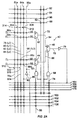
- FIG. 1 a simplified block diagram of an FPGA core architecture 10 is shown.
- core architecture refers to the architecture of the core of an FPGA array which comprises a plurality of logic function circuits or modules (reference numerals 12-1 to 12-12) arranged in a matrix with an overlay of interconnect architecture including interconnect conductors and user-programmable interconnect elements.
- the logic function modules 12-1 through 12-12 may comprise any of a variety of circuits, either combinational logic, sequential logic, or combinations thereof, and need not be identical, as will be disclosed in more detail herein.
- logic function modules 12-1 through 12-12 are disposed in a network of interconnect conductors.
- the network of interconnect conductors is shown in simplified schematic form.
- the architecture may be a "sea of gates" type architecture where the interconnect conductors actually run directly over, rather than between, the logic function circuits.
- the interconnect conductors will comprise metal lines in layers disposed over the layers which constitute the logic function circuits.
- Such a "sea of gates” architecture is known in the art and is exemplified by U.S. Patent No. 5,132,571 to McCollum et al. and permits the fabrication of a more dense array than an architecture in which the interconnect conductors run only between the logic function circuits.
- FIG. 1 depicts an interconnect architecture comprising a plurality of horizontal and vertical channels of interconnect conductors.
- horizontal channels are depicted as single lines identified by reference numerals 14-1, 14-2, 14-3, and 14-4
- vertical channels are depicted as single lines identified by reference numerals 16-1, 16-2, 16-3, and 16-4.
- each channel will comprise a plurality of individual interconnect conductors, some of which may be segmented and some of which may run the length (or width) of the array.
- the number of interconnect conductors present in each channel in any actual integrated circuit will be dictated by individual design choice, based upon such factors as array size and density.
- segmentation of interconnect conductors is known and is exemplified in prior art patents such as U.S. patent No. 4,758,745 to El Gamal et al. and 5,073,729 to Greene et al. and is thus not shown in FIG. 1 to avoid overcomplicating the figure.
- any one of the many available segmentation schemes may be employed in the architecture of the present invention.
- Such skilled persons will recognize that the segmented interconnect conductors may be selectively joined to make longer conductors by programming user-programmable interconnect elements between selected ones of the conductors.
- intersections of selected ones of the individual conductors horizontal and vertical interconnect channels are populated with user programmable interconnect elements which may be programmed by the user to make electrical connections between selected ones of them to implement connection nets between the inputs and the outputs of the logic function circuits.
- Groups of such user programmable interconnect elements at the intersections of the horizontal and vertical interconnect channels are shown schematically in FIG. 1 as squares 18-1 through 18-16.
- Inputs and outputs of the logic function circuits are also connectable to selected ones of the interconnect conductors in the channels by user-programmable interconnect elements disposed at the intersections of the individual inputs and outputs and selected ones of the interconnect conductors in the channels, as shown schematically by squares 20.
- FIG. 1 An important feature of the architecture of Fig 1 is a network of "local interconnect" channels which are shown running between adjacent pairs of logic function circuits in the matrix.
- these local interconnect channels are shown running between 12-1 and 12-2, 12-3 and 12-4, 12-5 and 12-6, 12-7 and 12-8, 12-9 and 12-10, 12-11 and 12-22, and are indicated by reference numerals 22-1 through 22-6.
- the local interconnect channels provide an enhanced interconnection capability between neighboring logic function circuits.
- the local interconnect channels may connect more than a single pair of adjacent logic modules.
- local interconnect channel 22-1 could also be used in conjunction with the general interconnect channels to make connections to logic modules 12-5 and 12-6 as will be seen more clearly from FIG. 2A.
- Selected ones of the individual local interconnect conductors are connectable to selected ones of the interconnect conductors in the channels by user-programmable interconnect elements placed at intersections thereof.
- the networks of these user-programmable interconnect elements are shown schematically in FIG. 1 as squares 24.
- I/O modules 26-1, 26-2, 26-3, and 26-4 are shown coupled between I/O pads 28-1, 28-2, 28-3, and 28-4, respectively, and horizontal interconnect channels 14-2 and 14-3 and vertical interconnect channels 16-2 and 16-3 respectively.
- I/O modules 26-1, 26-2, 26-3, and 26-4 each comprise an input buffer, an output buffer and input/output function select circuitry.
- the design of particular I/O module circuitry is simply a matter of design choice and is well within the level of ordinary skill in the art. Known examples of such circuitry may be found in United States Patent No. 5,083,083.
- Program and test control circuit 30 contains the necessary circuitry to accept programming data and control signals from off chip via I/O pads 32, 34, and 36. Those of ordinary skill in the art will recognize that the number of such I/O pads necessary for any actual implementation will vary according to design choice and requirements.
- the data and control signals are used to program selected ones of the user-programmable interconnect elements in the integrated circuit in order to define the circuit functions of the logic function modules 12-1 through 12-12 and the I/O modules 26-1 through 26-4 and the circuit connection paths between them.
- Program and test control circuit 30 may also be used to provide test data to and obtain test data from the logic function modules 12-1 through 12-12 as known in the art. Examples of testing using such circuitry are found in United States Patents 4,758,745 and 5,083,083.
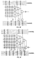
- a presently preferred embodiment of combinatorial unit 40 for the programmable logic module may comprise three two-input multiplexers 42, 44, and 46.
- First two-input multiplexer 42 has a first data input connected to a first data input node 48, a second data input connected to a second data input node 50, a control input connected to the output of a first gate 52, and an output 54.
- the first gate 52 has a first input connected to a first control input node 56 and a second input connected to a second control input node 58.
- Second two-input multiplexer 44 has a first data input connected to a third data input node 60, a second data input connected to a fourth data input node 62, a control input connected to the output of the first gate 52, and an output 66.
- Third two-input multiplexer 46 has a first data input connected to the output 54 of first multiplexer 42, a second data input connected to the output 66 of second multiplexer 44, a control input connected to the output of a second gate 68, and an output 70.
- the second gate has a first input connected to a third control input mode 72 and a second input connected to a fourth control input node 74.
- An output buffer 76 is connected to the output 70 of third multiplexer 46.
- First gate 52 and second gate 68 are shown as an AND and an OR gate, respectively, but persons of ordinary skill in the art will recognize that other gate combinations are possible.
- a plurality of interconnect conductors 78, 80, 82, 84, and 86 intersect the first through fourth data input nodes 48, 50, 60 and 62 and user-programmable interconnect elements (shown as hollow circles in the drawing figures) are preferably disposed at each intersection to allow programmable connections to be made between selected ones of the interconnect conductors and selected ones of the first through fourth data input nodes.
- Selected ones of the user-programmable interconnect elements are indicated by reference numerals 88a-88d and will be discussed later with reference to FIG. 2B.
- One of the plurality of interconnect conductors 86 is connected to another one of the interconnect conductors 84 through an inverter 90.
- inverter 90 adds to the versatility of the logic function module circuits by allowing a selected one of the input terms to be inverted. This versatility could be further increased by extending interconnect conductor 86 to cross other functional unit inputs in the same functional unit or by making it a part of the local interconnect channel to allow connections to other functional units.
- the output of inverter 90 can also be connected to any of the inputs of gates 52 and 68 through additional antifuses.
- the interconnect conductors 78, 80, 82, and 84 are shown intersecting horizontal interconnect conductors 92, 94, 96, and 98 in an upper general interconnect channel and horizontal interconnect conductors 100, 102, 104, and 106 in a lower general interconnect channel.
- the inputs 56, 58, 72, and 74 of the first and second gates also cross the horizontal interconnect conductors 92, 94, 96, 98, 100, 102, 104, and 106.
- Other user-programmable interconnect elements are disposed at the intersections of these conductors and may be programmed to selectively make connections as is known in the art.
- FIG. 2A is merely illustrative and that other arrangements using other numbers of interconnect conductors and other schemes for populating the conductor intersections with user-programmable interconnect elements are possible.
- the combinatorial unit 40 for the programmable logic module depicted in FIG. 2A is a compact and flexible circuit, capable of performing a wide variety of combinatorial logic functions.
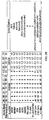
- FIG. 2B a table is presented showing the output states of the combinatorial logic function module block of FIG. 2A as a function of the states of its inputs for a small sampling of the available combinatorial functions possible using this unit.
- Those of ordinary skill in the art will be readily able to determine the remaining possible functions. Such skilled persons will also readily recognize that multiple implementations are possible for certain of these functions. In reading the Table of FIG.
- A0 and B0 represent the first and second inputs 56 and 58 of AND Gate 52
- A1 and B1 represent the first and second inputs 72 and 74 of OR Gate 68.
- the input lines L0, L1, L2, and L3 represent interconnect conductors 78, 80, 82, and 84, respectively.
- the inputs D0, D1, D2, and D3 represent the data input nodes 48, 50, 60 and 62, respectively, of the first and second multiplexers 42 and 44.
- the notation !L3 in the entries under "Internal" represent the output of inverter 90 on interconnect conductor 86.
- the entries in FIG. 2B are straightforward.
- the input terms “a” and “b” are presented to the first and second inputs of AND gate 52 on lines 56 and 58.
- the input term “c” is presented to one of the inputs 72 of OR gate 68 and a logic “0” is presented to the other input 74 of OR gate 68.
- Logic "0" levels are presented to interconnect conductors 78, 80, and 82, and the input term "d” is presented to interconnect conductor 84.
- D0 first data input node 48 to first input of first multiplexer 42
- interconnect conductor 78 This may be accomplished by programming user-programmable interconnect element 88a at the intersection of interconnect conductor 78 and first data input node 48.
- D1 second data input node 50 to second input of first multiplexer 42
- interconnect conductor 80 This may be accomplished by programming user-programmable interconnect element 88b at the intersection of interconnect conductor 80 and second data input node 50.
- D2 third data input node 60 to first input of second multiplexer 44
- the sequential logic unit 110 for a logic module according to the present invention is shown in block/schematic format.
- the sequential logic unit comprises three multiplexers and a D flip-flop.
- a first two input multiplexer 112 has a first data input connected to a first data input node 114, a second data input connected to a second data input node 116, a control input connected to a first control node 118, and an output 120.
- a second two input multiplexer 122 has a first data input connected to the output 120 of the first multiplexer, a second data input connected to the output of D flip-flop 124, a control input connected to a second control node 126, and an output 128 connected to the D input of the D flip-flop 124.
- a first four input multiplexer 130 has a first data input connected to a first clock input node 132, a second data input connected to the complement of the signal on first clock input node 132, a third data input connected to a second clock input at node 134, a fourth data input connected to the complement of the second clock input signal on node 134, a first control input connected to a clock select node 136, a second control input connected to a clock polarity select node 138, and an output 140 connected to the clock input of the D flip-flop.
- the output of D flip-flop 124 is buffered by buffer 142.
- D flip-flop 124 is also provided with set and reset inputs 144 and 146, respectively.
- sequential unit 110 of FIG. 2C is connectable to the interconnect architecture of the present invention.
- the various inputs and control inputs of the elements of sequential unit 110 are shown intersecting horizontal interconnect conductors 148, 150, 152, and 154, in an upper general interconnect channel and horizontal interconnect conductors 156, 158, 160, and 162 in a lower general interconnect channel.
- User-programmable interconnect elements are disposed at the intersections of these conductors and may be programmed to selectively make connections as is known in the art.
- sequential unit 110 is also a flexible circuit.
- First four-input multiplexer 130 is used to select and control the clock source so that the D flip-flop 124 can be driven from a system clock at first clock input node 132, which would preferably be common to all such units on an integrated circuit, or a clock signal from a clock node derived from other signals presented on second clock node 134 from the general interconnect channels.
- the second multiplexer control signal control node 138 to first four-input multiplexer 130 allows selection of rising or falling edge triggering for the D flip-flop 124.
- this function is also easily implemented by a third two-input multiplexer and an exclusive-OR gate.
- interconnect conductors 92, 94, 96, 98, 100, 102, 104, 106, 148, 150, 152, 154, 156, 158, 160, and 162 are local interconnect shared between neighboring logic function units.
- the outputs of the combinatorial unit 40 and the sequential unit 110 are hardwired to individual ones of the local interconnect conductors.
- the local interconnect conductors are given the same reference numerals in FIGS. 2A and 2C.
- four local interconnect conductors 164, 166, 168, and 170 are shown, although those of ordinary skill in the art will recognize that the number of local interconnect conductors to be used in any actual realization of the architecture of the present invention will be largely a matter of design choice and the number of combinational and sequential units in the locally interconnected logic modules.
- the output of buffer 76 of combinatorial unit 40 is shown hardwired to local interconnect conductor 164.
- the output of buffer 142 of sequential unit 110 is shown hardwired to local interconnect conductor 166.
- Selected ones of the other data and control inputs of combinatorial unit 40 and sequential unit 110 are shown connectable to local interconnect conductors 164, 166, 168, and 170 via user-programmable interconnect elements shown as circles at the intersections of the data and control inputs of combinatorial unit 40 and sequential unit 110 and local interconnect conductors 164, 166, 168, and 170.
- combinatorial unit 40 of FIG. 2A While it is presently preferred to employ the combinatorial unit 40 of FIG. 2A in the present invention, those of ordinary skill in the art will appreciate that other combinatorial units will be usefully employed in the architecture of the present invention. Referring now to FIGS. 3A-3F, alternative combinatorial unit circuits are presented.
- the logic module may comprise three combinatorial units or three sequential units, or may be mixed, i.e., the logic module may comprise one combinatorial unit and two sequential units.
- the logic module may be advantageous to internally connect the prebuffered output of the combinatorial unit to one of the inputs of the first multiplexer of the sequential unit. Such an arrangement is shown in FIG. 4A.
- logic function module 200 is depicted in block/schematic format.
- logic function module 200 is shown to include a combinatorial unit 40 and two sequential units 110a and 110b.
- the elements of these units depicted in FIG. 4A will be referred to using the same reference numerals used in FIGS. 2A and 2C, although not all elements are numbered in FIG. 4A to avoid overcrowding the drawing.
- An upper general interconnect channel includes general interconnect conductors 202, 204, 206, 208, and 210, some of which may be dedicated to clock signal and dedicated logic level functions, and a lower general interconnect channel includes general interconnect conductors 212, 214, 216, 218, and 220,some of which may also be dedicated to clock signal and dedicated logic level functions.
- a local interconnect channel 222 includes local interconnect conductors 224, 226, 228, 230, 232 and 234.
- the output of output buffer 76 of combinatorial unit 40 is shown hardwired to local interconnect conductor 224.
- the output of output buffer 142a of combinational unit 110a is shown hardwired to local interconnect conductor 226.
- output buffer 142b of combinatorial unit 110b is shown hardwired to local interconnect conductor 228.
- an internal hardwired connection is shown made between the pre-buffered output of combinatorial unit 40 and the first input 114a of multiplexer 112a in sequential unit 110a.
- the pre-buffered output of combinatorial unit 40 can be hardwired to the control input of multiplexer 112a.
- the logic function module of FIG. 4A is extremely flexible and permits implementation of a wide variety of combinatorial and sequential logic functions.
- the advantage of the local interconnect channel becomes apparent.
- the outputs of the combinatorial and sequential elements are individually hardwired to different ones of local interconnect conductors 224, 226, 228, 230, 232, and 234. Because the hardwired connections bypass any user-programmable interconnect elements in the general interconnect channels, any time delay which such interconnect elements will normally introduce to signals passing through them are eliminated, resulting in a circuit which is, in effect, a larger, faster, single logic function module.
- FIG. 4A also illustrates the extra versatility which the addition of inverter 90 of FIG. 2A adds to the logic module function.
- the inverter 90 shown physically located in the combinatorial unit may be used with the combinatorial unit or with either sequential unit 110a and 110b by programming appropriate antifuses to connect its output to the data inputs and control inputs of the data multiplexers 112a, 122a associated with sequential unit 110a and 112b and 122b associated with sequential unit 110b and to the set and reset inputs of the D flip-flops 124a and 124b in the sequential units.
- the mixture and placement of the combinatorial and sequential components of pairs of logic function may be advantageously varied.
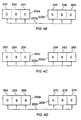
- This aspect of the invention is illustrated in FIGS. 4B-4D, schematic representations of the layouts of logic function module pairs connected by local interconnect channels according to the present invention.
- a logic function module pair comprising logic function modules 200a and 200b are shown connected by local interconnect bus 222a.
- Logic function module 200a comprises a leftmost combinatorial unit 240, a center sequential unit 242, and a rightmost combinatorial unit 244.
- Logic function module 200b comprises a leftmost combinatorial unit 246, a center sequential unit 248, and a rightmost combinatorial unit 250.
- FIGS. 4C and 4D Other variations of the logic module pair layout according to the present invention are shown in FIGS. 4C and 4D.
- a logic function module pair comprising logic function modules 200c and 200d are shown connected by local interconnect bus 222b.
- Logic function module 200c comprises a leftmost combinatorial unit 252, a center sequential unit 254, and a rightmost combinatorial unit 256.
- Logic function module 200d comprises a leftmost sequential unit 258, a center sequential unit 260, and a rightmost combinatorial unit 262.
- FIG. 4D a logic function module pair comprising logic function modules 200e and 200f are shown connected by local interconnect bus 222c.
- Logic function module 200e comprises a leftmost combinatorial unit 264, a center sequential unit 266, and a rightmost sequential unit 268.
- Logic function module 200f comprises a leftmost combinatorial unit 270, a center sequential unit 272, and a rightmost combinatorial unit 274.
- the interconnect conductors of the interconnect architecture of the present invention may be supplied as segments.
- the ability to temporarily connect the segments together for purposes such as testing may be provided.
- user-programmable interconnect elements may be provided to programmably connect the segments together to produce longer interconnect conductors during normal operation of the integrated circuit.
- each of interconnect conductors 78, 80, 82, 84, and 86 are divided into segments by pass transistors.
- interconnect conductor 78 is connected to one of the source/drain terminals of pass transistor 302.
- the other source/drain terminal of pass transistor 302 is connected to interconnect conductor 78a, which may be considered as a downwardly extending vertical extension of interconnect conductor 78.
- interconnect conductor 80 is connected to one of the source/drain terminals of pass transistor 304.
- the other source/drain terminal of pass transistor 304 is connected to interconnect conductor 80a, which may be considered as an upwardly extending vertical extension of interconnect conductor 80.
- Interconnect conductor 82 is connected to one of the source/drain terminals of pass transistor 306.
- the other source/drain terminal of pass transistor 306 is connected to interconnect conductor 82a, which may be considered as a downwardly extending vertical extension of interconnect conductor 82.
- Interconnect conductor 84 is connected to one of the source/drain terminals of pass transistor 308.
- the other source/drain terminal of pass transistor 308 is connected to interconnect conductor 84a, which may be considered as an upwardly extending vertical extension of interconnect conductor 84.
- Interconnect conductor 86 is connected to one of the source/drain terminals of pass transistor 310.
- the other source/drain terminal of pass transistor 310 is connected to interconnect conductor 86a, which may be considered as an upwardly extending vertical extension of interconnect conductor 86.
- the locations of the pass transistors are preferably staggered to add to the versatility of the interconnect architecture.
- pass transistors 302 and 306 are located at one vertical position on their associated interconnect conductors while pass transistors 304, 308, and 310 are located at another vertical position on their associated interconnect conductors.
- the gates of the pass transistors are driven by the program and test control circuit 30 (FIG. 1). While the gates of pass transistors 302 and 306 are shown connected to a common gate line 312 and the gates of pass transistors 304, 308, and 310 are shown connected to a common gate line 314, those of ordinary skill in the art will recognize that other arrangements are possible.
- interconnect conductors 78a and 82a will be connectable through user-programmable interconnect elements to the logic function module (not shown in FIG. 2A) located below logic function module 40 in the integrated circuit array and that interconnect conductors 80a, 84a, and 86a will be connectable through user-programmable interconnect elements to the logic function module (not shown in FIG. 2A) located above logic function module 40 in the integrated circuit array.
- the particular segmentation scheme used in an actual architecture fabricated according to the present invention will be somewhat arbitrary and largely a matter of design choice dictated by the particular architectural layout.
- the sequential logic unit of the invention may further comprise a clock multiplexer having a first data input connected to a global clock conductor, a second data input connected to the complement of the signal on said global clock conductor, a third data input connected to a clock input conductor, a fourth data input connected to the complement of the signal on said clock input conductor, a first control input connected to a clock select control input conductor, a second control input connected to a clock polarity control input conductor, and an output connected to said clock input of said data flip-flop.
- the programmable logic module of the invention may further comprise a clock multiplexer having a first data input connected to a global clock conductor, a second data input connected to the complement of the signal on said global clock conductor, a third data input connected to a clock input conductor, a fourth data input connected to the complement of the signal on said clock input conductor, a first control input connected to a clock select control input conductor, a second control input connected to a clock polarity control input conductor and an output connected to said clock input of said data flip-flop.
- a clock multiplexer having a first data input connected to a global clock conductor, a second data input connected to the complement of the signal on said global clock conductor, a third data input connected to a clock input conductor, a fourth data input connected to the complement of the signal on said clock input conductor, a first control input connected to a clock select control input conductor, a second control input connected to a clock polarity control input conductor and an output connected to said clock input of said data flip-
- the programmable logic module may yet further comprise a second clock multiplexer having a first data input connected to a global clock conductor, a second data input connected to the complement of the signal on said global clock conductor, a third data input connected to a clock input conductor, a fourth data input connected to the complement of the signal on said clock input conductor, a first control input connected to a clock select control input conductor, a second control input connected to a clock polarity control input conductor, and an output connected to said clock input of said data flip-flop.
Abstract
Description
Claims (9)
- A combinatorial logic unit comprising:a first multiplexer having a first data input connected to a first data input conductor, a second data input connected to a second data input conductor, a control input, and an output;a second multiplexer having a first data input connected to a third data input conductor, a second data input connected to a fourth data input conductor, a control input, and an output;a third multiplexer having a first data input connected to the output of said first multiplexer, a second data input connected to the output of said second multiplexer, a control input and an output;a first logic gate having a first input connected to a fifth data input conductor, a second input connected to a sixth data input conductor and an output connected to the control inputs of said first and second multiplexers;a second logic gate having a first input connected to a seventh data input conductor, a second input connected to an eighth data input conductor and an output connected to the control input of said third multiplexer;an output buffer having an input connected to said output of said third multiplexer and an output connected to an output conductor;a plurality of interconnect conductors intersecting said data and control input conductors of said first, second, and third multiplexers, said plurality of interconnect conductors selectively connectable to individual ones of said data and control input conductors by user-programmable interconnect elements; andan inverter having an input connected to a first one of said interconnect conductors and an output connected to a second one of said interconnect conductors.
- A sequential logic unit comprising:a data flip-flop having a data input, a clock input, and an output;a first data multiplexer having a first data input connected to a first data input conductor, a second data input connected to a second data input conductor, a control input connected to a first control input conductor, and an output;a second data multiplexer having a first data input connected to the output of said data flip-flop, a second data input connected to said output of said first multiplexer, a control input, and an output connected to the data input of said data flip-flop;an output buffer having an input connected to said output of said data flip-flop output, and an output connected to an output conductor; anda plurality of general interconnect conductors, at least some of said general interconnect conductors intersecting said data, clock, and control input conductors of said first and second multiplexers, said plurality of general interconnect conductors selectively connectable to individual ones of said data, clock and control input conductors by user-programmable interconnect elements.
- A sequential logic unit according to claim 2, further including:a set input connected to a set input conductor, said set input conductor intersecting at least some of said general interconnect conductors and connectable to least some of said general interconnect conductors by user programmable interconnect elements; anda reset input connected to a reset input conductor, said reset input conductor intersecting at least some of said general interconnect conductors and connectable to least some of said general interconnect conductors by user-programmable interconnect elements.
- A programmable logic module comprising:a first multiplexer having a first data input connected to a first data input conductor, a second data input connected to a second data input conductor, a control input and an output;a second multiplexer having a first data input connected to a third data input conductor, a second data input connected to a fourth data input conductor, a control input, and an output;a third multiplexer having a first data input connected to the output of said first multiplexer, a second data input connected to the output of said second multiplexer, a control input, and an output;a first logic gate having a first input connected to a fifth data input conductor, a second input connected to a sixth data input conductor and an output connected to the control inputs of said first and second multiplexers;a second logic gate having a first input connected to a seventh data input conductor, a second input connected to an eighth data input conductor and an output connected to the control input of said third multiplexer;a first output buffer having an input connected to said output of said third multiplexer and an output connected to a first output conductor;a data flip-flop having a data input, a clock input, and an output;a fourth data multiplexer having a first data input connected to the output of said first output butter, a second data input connected to a ninth data input conductor, a control input connected to a first control input conductor, and an output;a fifth data multiplexer having a first data input connected the output of said data flip-flop, a second data input connected to the output of said fourth multiplexer, a control input connected to a second control input conductor, and an output connected to the data input of said data flip-flop;a second output buffer having an input connected to said output of said data flip-flop output, and an output connected to a second output conductor;a plurality of general interconnect conductors, at least some of said general interconnect conductors intersecting said data, clock, and control input conductors of said first, second, third, fourth and fifth multiplexers and said first and second output buffers, said plurality of general interconnect conductors selectively connectable to individual ones of said data, clock, and control input conductors by user-programmable interconnect elements; andan inverter having an input connected to a first one of said interconnect conductors and an output connected to a second one of said interconnect conductors.
- A programmable logic module according to claim 4 and further comprising:a plurality of local interconnect conductors, a first one of said local interconnect conductors connected to the output of said first output buffer, a second one of said local interconnect conductors connected to the output of said second output buffer, at least some of said local interconnect conductors intersecting said data, clock, and control input conductors of said first, second, third, fourth and fifth multiplexers, said plurality of general interconnect conductors selectively connectable to individual ones of said data, clock, and control input conductors by user-programmable interconnect elements; andan inverter having an input connected to a first one of said interconnect conductors and an output connected to a second one of said interconnect conductors.
- A programmable logic module according to claim 5 and further comprising:a second data flip-flop having a data input, a clock input, and an output;a sixth data multiplexer having a first data input connected to a tenth data input conductor, a second data input connected to an eleventh data input conductor, a control input connected to a fourth control input conductor, and an output;a seventh data multiplexer having a first data input connected the output of said second data flip-flop, a second data input connected to the output of said fourth multiplexer, a control input connected to a fifth control input conductor, and an output connected to the data input of said second data flip-flop;a third output buffer having an input connected to said output of said second data flip-flop, and an output connected to an output conductor;a plurality of user-programmable interconnect elements disposed at selected ones of said first and second intersections.
- A programmable logic module according to claim 4, 5 or 6 wherein the or a data flip-flop further includes:a set input connected to a set input conductor, said set input conductor intersecting at least some of said general interconnect conductors and connectable to least some of said general interconnect conductors by user-programmable interconnect elements; anda reset input connected to a reset input conductor, said reset input conductor intersecting at least some of said general interconnect conductors and connectable to least some of said general interconnect conductors by user-programmable interconnect elements.
- A unit according to claim 1 or a module according to claim 4, 5, 6 or 7 wherein said first logic gate is an AND gate and said second logic gate is an OR gate.
- A unit or module according to any one of the preceding claims wherein said user programmable interconnect elements are antifuses.
Applications Claiming Priority (3)
| Application Number | Priority Date | Filing Date | Title |
|---|---|---|---|
| US246218 | 1994-05-19 | ||
| US08/246,218 US5451887A (en) | 1986-09-19 | 1994-05-19 | Programmable logic module and architecture for field programmable gate array device |
| EP95303345A EP0683565B1 (en) | 1994-05-19 | 1995-05-18 | Programmable architecture for field programmable gate array device |
Related Parent Applications (1)
| Application Number | Title | Priority Date | Filing Date |
|---|---|---|---|
| EP95303345A Division EP0683565B1 (en) | 1994-05-19 | 1995-05-18 | Programmable architecture for field programmable gate array device |
Publications (2)
| Publication Number | Publication Date |
|---|---|
| EP0889593A1 true EP0889593A1 (en) | 1999-01-07 |
| EP0889593B1 EP0889593B1 (en) | 2002-09-25 |
Family
ID=22929777
Family Applications (2)
| Application Number | Title | Priority Date | Filing Date |
|---|---|---|---|
| EP95303345A Expired - Lifetime EP0683565B1 (en) | 1994-05-19 | 1995-05-18 | Programmable architecture for field programmable gate array device |
| EP98114150A Expired - Lifetime EP0889593B1 (en) | 1994-05-19 | 1995-05-18 | Programmable logic module for field programmable gate array device |
Family Applications Before (1)
| Application Number | Title | Priority Date | Filing Date |
|---|---|---|---|
| EP95303345A Expired - Lifetime EP0683565B1 (en) | 1994-05-19 | 1995-05-18 | Programmable architecture for field programmable gate array device |
Country Status (4)
| Country | Link |
|---|---|
| US (2) | US5451887A (en) |
| EP (2) | EP0683565B1 (en) |
| JP (1) | JP3589501B2 (en) |
| DE (2) | DE69507851T2 (en) |
Cited By (12)
| Publication number | Priority date | Publication date | Assignee | Title |
|---|---|---|---|---|
| US6038627A (en) * | 1998-03-16 | 2000-03-14 | Actel Corporation | SRAM bus architecture and interconnect to an FPGA |
| US6549035B1 (en) | 1998-09-15 | 2003-04-15 | Actel Corporation | High density antifuse based partitioned FPGA architecture |
| US6727726B1 (en) | 2002-11-12 | 2004-04-27 | Actel Corporation | Field programmable gate array architecture including a buffer module and a method of distributing buffer modules in a field programmable gate array |
| US6750674B1 (en) | 2002-10-02 | 2004-06-15 | Actel Corporation | Carry chain for use between logic modules in a field programmable gate array |
| US6765427B1 (en) | 2002-08-08 | 2004-07-20 | Actel Corporation | Method and apparatus for bootstrapping a programmable antifuse circuit |
| US6772387B1 (en) | 1998-03-16 | 2004-08-03 | Actel Corporation | Cyclic redundancy checking of a field programmable gate array having an SRAM memory architecture |
| US6774667B1 (en) | 2002-05-09 | 2004-08-10 | Actel Corporation | Method and apparatus for a flexible chargepump scheme for field-programmable gate arrays |
| US6799240B1 (en) | 1998-03-16 | 2004-09-28 | Actel Corporation | SRAM bus architecture and interconnect to an FPGA |
| US6825690B1 (en) | 2003-05-28 | 2004-11-30 | Actel Corporation | Clock tree network in a field programmable gate array |
| US6980027B2 (en) | 2003-05-28 | 2005-12-27 | Actel Corporation | Synchronous first-in/first-out block memory for a field programmable gate array |
| US7389487B1 (en) | 1998-04-28 | 2008-06-17 | Actel Corporation | Dedicated interface architecture for a hybrid integrated circuit |
| US7774665B2 (en) | 2002-09-03 | 2010-08-10 | Actel Corporation | Apparatus for testing a phrase-locked loop in a boundary scan enabled device |
Families Citing this family (88)
| Publication number | Priority date | Publication date | Assignee | Title |
|---|---|---|---|---|
| US5477165A (en) * | 1986-09-19 | 1995-12-19 | Actel Corporation | Programmable logic module and architecture for field programmable gate array device |
| US5451887A (en) * | 1986-09-19 | 1995-09-19 | Actel Corporation | Programmable logic module and architecture for field programmable gate array device |
| GB8906145D0 (en) * | 1989-03-17 | 1989-05-04 | Algotronix Ltd | Configurable cellular array |
| US5198705A (en) | 1990-05-11 | 1993-03-30 | Actel Corporation | Logic module with configurable combinational and sequential blocks |
| GB9223226D0 (en) * | 1992-11-05 | 1992-12-16 | Algotronix Ltd | Improved configurable cellular array (cal ii) |
| US6154053A (en) * | 1993-09-02 | 2000-11-28 | Xilinx, Inc. | Look-ahead carry structure with homogeneous CLB structure and pitch larger than CLB pitch |
| US5546018A (en) * | 1993-09-02 | 1996-08-13 | Xilinx, Inc. | Fast carry structure with synchronous input |
| US5898319A (en) * | 1993-09-02 | 1999-04-27 | Xilinx, Inc. | Method and structure for providing fast conditional sum in a field programmable gate array |
| US6288570B1 (en) | 1993-09-02 | 2001-09-11 | Xilinx, Inc. | Logic structure and circuit for fast carry |
| IL109491A (en) * | 1994-05-01 | 1999-11-30 | Quick Tech Ltd | Customizable logic array device |
| US5633601A (en) * | 1995-03-10 | 1997-05-27 | Texas Instruments Incorporated | Field programmable gate array logic module configurable as combinational or sequential circuits |
| US5751162A (en) * | 1995-04-06 | 1998-05-12 | Texas Instruments Incorporated | Field programmable gate array logic module configurable as combinational or sequential circuits |
| US5594363A (en) * | 1995-04-07 | 1997-01-14 | Zycad Corporation | Logic cell and routing architecture in a field programmable gate array |
| US5530378A (en) * | 1995-04-26 | 1996-06-25 | Xilinx, Inc. | Cross point interconnect structure with reduced area |
| US5528169A (en) * | 1995-04-26 | 1996-06-18 | Xilinx, Inc. | Method and structure for providing a flip flop circuit with a configurable data input path |
| US6028446A (en) * | 1995-06-06 | 2000-02-22 | Advanced Micro Devices, Inc. | Flexible synchronous and asynchronous circuits for a very high density programmable logic device |
| US5751165A (en) * | 1995-08-18 | 1998-05-12 | Chip Express (Israel) Ltd. | High speed customizable logic array device |
| US5684412A (en) * | 1995-08-18 | 1997-11-04 | Chip Express (Israel) Ltd. | Cell forming part of a customizable logic array |
| US5936426A (en) | 1997-02-03 | 1999-08-10 | Actel Corporation | Logic function module for field programmable array |
| US6150837A (en) * | 1997-02-28 | 2000-11-21 | Actel Corporation | Enhanced field programmable gate array |
| US6014038A (en) * | 1997-03-21 | 2000-01-11 | Lightspeed Semiconductor Corporation | Function block architecture for gate array |
| US6130555A (en) * | 1997-10-13 | 2000-10-10 | Altera Corporation | Driver circuitry for programmable logic devices |
| US6223313B1 (en) | 1997-12-05 | 2001-04-24 | Lightspeed Semiconductor Corporation | Method and apparatus for controlling and observing data in a logic block-based asic |
| US6611932B2 (en) | 1997-12-05 | 2003-08-26 | Lightspeed Semiconductor Corporation | Method and apparatus for controlling and observing data in a logic block-based ASIC |
| US6137308A (en) * | 1998-01-20 | 2000-10-24 | Cypress Semiconductor Corporation | Programmable interconnect matrix architecture for complex programmable logic device |
| US6169416B1 (en) | 1998-09-01 | 2001-01-02 | Quicklogic Corporation | Programming architecture for field programmable gate array |
| US6204686B1 (en) * | 1998-12-16 | 2001-03-20 | Vantis Corporation | Methods for configuring FPGA's having variable grain blocks and shared logic for providing symmetric routing of result output to differently-directed and tristateable interconnect resources |
| US6762621B1 (en) * | 1998-12-31 | 2004-07-13 | Actel Corporation | Programmable multi-standard I/O architecture for FPGAs |
| US6388464B1 (en) | 1999-12-30 | 2002-05-14 | Cypress Semiconductor Corp. | Configurable memory for programmable logic circuits |
| US6864710B1 (en) | 1999-12-30 | 2005-03-08 | Cypress Semiconductor Corp. | Programmable logic device |
| US6608500B1 (en) | 2000-03-31 | 2003-08-19 | Cypress Semiconductor Corp. | I/O architecture/cell design for programmable logic device |
| US6870396B2 (en) * | 2000-09-02 | 2005-03-22 | Actel Corporation | Tileable field-programmable gate array architecture |
| US6476636B1 (en) | 2000-09-02 | 2002-11-05 | Actel Corporation | Tileable field-programmable gate array architecture |
| US6937063B1 (en) | 2000-09-02 | 2005-08-30 | Actel Corporation | Method and apparatus of memory clearing with monitoring RAM memory cells in a field programmable gated array |
| US7426665B1 (en) | 2000-09-02 | 2008-09-16 | Actel Corporation | Tileable field-programmable gate array architecture |
| US7015719B1 (en) | 2000-09-02 | 2006-03-21 | Actel Corporation | Tileable field-programmable gate array architecture |
| US8103496B1 (en) | 2000-10-26 | 2012-01-24 | Cypress Semicondutor Corporation | Breakpoint control in an in-circuit emulation system |
| US8149048B1 (en) | 2000-10-26 | 2012-04-03 | Cypress Semiconductor Corporation | Apparatus and method for programmable power management in a programmable analog circuit block |
| US6724220B1 (en) | 2000-10-26 | 2004-04-20 | Cyress Semiconductor Corporation | Programmable microcontroller architecture (mixed analog/digital) |
| US8176296B2 (en) * | 2000-10-26 | 2012-05-08 | Cypress Semiconductor Corporation | Programmable microcontroller architecture |
| US7765095B1 (en) | 2000-10-26 | 2010-07-27 | Cypress Semiconductor Corporation | Conditional branching in an in-circuit emulation system |
| EP1365923B2 (en) * | 2001-02-28 | 2009-11-11 | DataLase Ltd | Laser coding |
| US7558967B2 (en) * | 2001-09-13 | 2009-07-07 | Actel Corporation | Encryption for a stream file in an FPGA integrated circuit |
| US7406674B1 (en) | 2001-10-24 | 2008-07-29 | Cypress Semiconductor Corporation | Method and apparatus for generating microcontroller configuration information |
| US6696856B1 (en) | 2001-10-30 | 2004-02-24 | Lightspeed Semiconductor Corporation | Function block architecture with variable drive strengths |
| US8078970B1 (en) | 2001-11-09 | 2011-12-13 | Cypress Semiconductor Corporation | Graphical user interface with user-selectable list-box |
| US8042093B1 (en) | 2001-11-15 | 2011-10-18 | Cypress Semiconductor Corporation | System providing automatic source code generation for personalization and parameterization of user modules |
| US7774190B1 (en) | 2001-11-19 | 2010-08-10 | Cypress Semiconductor Corporation | Sleep and stall in an in-circuit emulation system |
| US6971004B1 (en) | 2001-11-19 | 2005-11-29 | Cypress Semiconductor Corp. | System and method of dynamically reconfiguring a programmable integrated circuit |
| US8069405B1 (en) | 2001-11-19 | 2011-11-29 | Cypress Semiconductor Corporation | User interface for efficiently browsing an electronic document using data-driven tabs |
| US7770113B1 (en) | 2001-11-19 | 2010-08-03 | Cypress Semiconductor Corporation | System and method for dynamically generating a configuration datasheet |
| US7844437B1 (en) | 2001-11-19 | 2010-11-30 | Cypress Semiconductor Corporation | System and method for performing next placements and pruning of disallowed placements for programming an integrated circuit |
| US8103497B1 (en) | 2002-03-28 | 2012-01-24 | Cypress Semiconductor Corporation | External interface for event architecture |
| US7308608B1 (en) | 2002-05-01 | 2007-12-11 | Cypress Semiconductor Corporation | Reconfigurable testing system and method |
| US6777977B1 (en) | 2002-05-01 | 2004-08-17 | Actel Corporation | Three input field programmable gate array logic circuit configurable as a three input look up table, a D-latch or a D flip-flop |
| US6891394B1 (en) * | 2002-06-04 | 2005-05-10 | Actel Corporation | Field-programmable gate array low voltage differential signaling driver utilizing two complimentary output buffers |
| US7378867B1 (en) | 2002-06-04 | 2008-05-27 | Actel Corporation | Field-programmable gate array low voltage differential signaling driver utilizing two complimentary output buffers |
| US7761845B1 (en) | 2002-09-09 | 2010-07-20 | Cypress Semiconductor Corporation | Method for parameterizing a user module |
| US7269814B1 (en) | 2002-10-08 | 2007-09-11 | Actel Corporation | Parallel programmable antifuse field programmable gate array device (FPGA) and a method for programming and testing an antifuse FPGA |
| US6774670B1 (en) | 2002-12-30 | 2004-08-10 | Actel Corporation | Intra-tile buffer system for a field programmable gate array |
| US6800884B1 (en) * | 2002-12-30 | 2004-10-05 | Actel Corporation | Inter-tile buffer system for a field programmable gate array |
| US6774672B1 (en) | 2002-12-30 | 2004-08-10 | Actel Corporation | Field-programmable gate array architecture |
| US6774669B1 (en) | 2002-12-30 | 2004-08-10 | Actel Corporation | Field programmable gate array freeway architecture |
| US6943581B1 (en) * | 2003-03-27 | 2005-09-13 | Xilinx, Inc. | Test methodology for direct interconnect with multiple fan-outs |
| US7385419B1 (en) | 2003-05-30 | 2008-06-10 | Actel Corporation | Dedicated input/output first in/first out module for a field programmable gate array |
| US7796464B1 (en) | 2003-06-27 | 2010-09-14 | Cypress Semiconductor Corporation | Synchronous memory with a shadow-cycle counter |
| US7295049B1 (en) | 2004-03-25 | 2007-11-13 | Cypress Semiconductor Corporation | Method and circuit for rapid alignment of signals |
| US7243329B2 (en) * | 2004-07-02 | 2007-07-10 | Altera Corporation | Application-specific integrated circuit equivalents of programmable logic and associated methods |
| US8069436B2 (en) | 2004-08-13 | 2011-11-29 | Cypress Semiconductor Corporation | Providing hardware independence to automate code generation of processing device firmware |
| US7332976B1 (en) | 2005-02-04 | 2008-02-19 | Cypress Semiconductor Corporation | Poly-phase frequency synthesis oscillator |
| US7400183B1 (en) | 2005-05-05 | 2008-07-15 | Cypress Semiconductor Corporation | Voltage controlled oscillator delay cell and method |
| US8085067B1 (en) | 2005-12-21 | 2011-12-27 | Cypress Semiconductor Corporation | Differential-to-single ended signal converter circuit and method |
| US8067948B2 (en) | 2006-03-27 | 2011-11-29 | Cypress Semiconductor Corporation | Input/output multiplexer bus |
| US8040266B2 (en) | 2007-04-17 | 2011-10-18 | Cypress Semiconductor Corporation | Programmable sigma-delta analog-to-digital converter |
| US9564902B2 (en) | 2007-04-17 | 2017-02-07 | Cypress Semiconductor Corporation | Dynamically configurable and re-configurable data path |
| US8026739B2 (en) | 2007-04-17 | 2011-09-27 | Cypress Semiconductor Corporation | System level interconnect with programmable switching |
| US7737724B2 (en) * | 2007-04-17 | 2010-06-15 | Cypress Semiconductor Corporation | Universal digital block interconnection and channel routing |
| US8516025B2 (en) | 2007-04-17 | 2013-08-20 | Cypress Semiconductor Corporation | Clock driven dynamic datapath chaining |
| US8130025B2 (en) | 2007-04-17 | 2012-03-06 | Cypress Semiconductor Corporation | Numerical band gap |
| US8092083B2 (en) | 2007-04-17 | 2012-01-10 | Cypress Semiconductor Corporation | Temperature sensor with digital bandgap |
| US9720805B1 (en) | 2007-04-25 | 2017-08-01 | Cypress Semiconductor Corporation | System and method for controlling a target device |
| US8065653B1 (en) | 2007-04-25 | 2011-11-22 | Cypress Semiconductor Corporation | Configuration of programmable IC design elements |
| US8266575B1 (en) | 2007-04-25 | 2012-09-11 | Cypress Semiconductor Corporation | Systems and methods for dynamically reconfiguring a programmable system on a chip |
| US8049569B1 (en) | 2007-09-05 | 2011-11-01 | Cypress Semiconductor Corporation | Circuit and method for improving the accuracy of a crystal-less oscillator having dual-frequency modes |
| US7893772B1 (en) | 2007-12-03 | 2011-02-22 | Cypress Semiconductor Corporation | System and method of loading a programmable counter |
| US9448964B2 (en) | 2009-05-04 | 2016-09-20 | Cypress Semiconductor Corporation | Autonomous control in a programmable system |
| FR2954023B1 (en) * | 2009-12-14 | 2012-02-10 | Lyon Ecole Centrale | INTERCONNECTED MATRIX OF RECONFIGURABLE LOGIC CELLS WITH CROSS INTERCONNECTION TOPOLOGY |
| US20160358653A1 (en) * | 2015-06-08 | 2016-12-08 | Altera Corporation | Hardware programmable device with integrated search engine |
Citations (3)
| Publication number | Priority date | Publication date | Assignee | Title |
|---|---|---|---|---|
| EP0415542A2 (en) * | 1989-08-15 | 1991-03-06 | Advanced Micro Devices, Inc. | Programmable gate array with improved interconnect structure, input/output structure and configurable logic block |
| US5198705A (en) * | 1990-05-11 | 1993-03-30 | Actel Corporation | Logic module with configurable combinational and sequential blocks |
| US5208491A (en) * | 1992-01-07 | 1993-05-04 | Washington Research Foundation | Field programmable gate array |
Family Cites Families (79)
| Publication number | Priority date | Publication date | Assignee | Title |
|---|---|---|---|---|
| US3818452A (en) * | 1972-04-28 | 1974-06-18 | Gen Electric | Electrically programmable logic circuits |
| US3816725A (en) * | 1972-04-28 | 1974-06-11 | Gen Electric | Multiple level associative logic circuits |
| US3849638A (en) * | 1973-07-18 | 1974-11-19 | Gen Electric | Segmented associative logic circuits |
| US3987287A (en) * | 1974-12-30 | 1976-10-19 | International Business Machines Corporation | High density logic array |
| NL7612223A (en) | 1976-11-04 | 1978-05-08 | Philips Nv | INTEGRATED CIRCUIT. |
| US4207556A (en) * | 1976-12-14 | 1980-06-10 | Nippon Telegraph And Telephone Public Corporation | Programmable logic array arrangement |
| FR2440657A1 (en) * | 1978-10-31 | 1980-05-30 | Ibm France | IMPROVEMENT ON MULTI-FUNCTION PROGRAMMABLE LOGIC NETWORKS |
| US4293783A (en) * | 1978-11-01 | 1981-10-06 | Massachusetts Institute Of Technology | Storage/logic array |
| JPS57111044A (en) * | 1980-12-27 | 1982-07-10 | Fujitsu Ltd | Master-slice type lsi device |
| US4433331A (en) * | 1981-12-14 | 1984-02-21 | Bell Telephone Laboratories, Incorporated | Programmable logic array interconnection matrix |
| US4541067A (en) | 1982-05-10 | 1985-09-10 | American Microsystems, Inc. | Combinational logic structure using PASS transistors |
| US4717912A (en) * | 1982-10-07 | 1988-01-05 | Advanced Micro Devices, Inc. | Apparatus for producing any one of a plurality of signals at a single output |
| US4847732A (en) * | 1983-09-15 | 1989-07-11 | Mosaic Systems, Inc. | Wafer and method of making same |
| GB8400959D0 (en) * | 1984-01-13 | 1984-02-15 | British Petroleum Co Plc | Semiconductor device |
| US4870302A (en) | 1984-03-12 | 1989-09-26 | Xilinx, Inc. | Configurable electrical circuit having configurable logic elements and configurable interconnects |
| JPH0772744B2 (en) * | 1984-09-04 | 1995-08-02 | 株式会社日立製作所 | Semiconductor integrated circuit device |
| US4642487A (en) * | 1984-09-26 | 1987-02-10 | Xilinx, Inc. | Special interconnect for configurable logic array |
| US4713557A (en) * | 1984-09-26 | 1987-12-15 | Xilinx, Inc. | Bidirectional buffer amplifier |
| DE3577953D1 (en) * | 1984-09-28 | 1990-06-28 | Siemens Ag | CIRCUIT FOR LOGIC GENERATION WITH MULTIPLEXERS. |
| US4706216A (en) * | 1985-02-27 | 1987-11-10 | Xilinx, Inc. | Configurable logic element |
| US4933577A (en) * | 1985-03-22 | 1990-06-12 | Advanced Micro Devices, Inc. | Output circuit for a programmable logic array |
| US5151623A (en) * | 1985-03-29 | 1992-09-29 | Advanced Micro Devices, Inc. | Programmable logic device with multiple, flexible asynchronous programmable logic blocks interconnected by a high speed switch matrix |
| US4963768A (en) * | 1985-03-29 | 1990-10-16 | Advanced Micro Devices, Inc. | Flexible, programmable cell array interconnected by a programmable switch matrix |
| US4742252A (en) * | 1985-03-29 | 1988-05-03 | Advanced Micro Devices, Inc. | Multiple array customizable logic device |
| US4677318A (en) * | 1985-04-12 | 1987-06-30 | Altera Corporation | Programmable logic storage element for programmable logic devices |
| US4691161A (en) * | 1985-06-13 | 1987-09-01 | Raytheon Company | Configurable logic gate array |
| US4763020B1 (en) * | 1985-09-06 | 1997-07-08 | Ricoh Kk | Programmable logic device having plural programmable function cells |
| EP0243486A1 (en) * | 1985-10-29 | 1987-11-04 | 4C Electronics, Inc. | Programmable integrated crosspoint switch |
| GB2188175B (en) * | 1986-03-18 | 1990-02-07 | Stc Plc | Data processing arrangement |
| US4823181A (en) * | 1986-05-09 | 1989-04-18 | Actel Corporation | Programmable low impedance anti-fuse element |
| US4789951A (en) * | 1986-05-16 | 1988-12-06 | Advanced Micro Devices, Inc. | Programmable array logic cell |
| JPS6341048A (en) * | 1986-08-06 | 1988-02-22 | Mitsubishi Electric Corp | Standard cell system large-scale integrated circuit |
| US5367208A (en) * | 1986-09-19 | 1994-11-22 | Actel Corporation | Reconfigurable programmable interconnect architecture |
| US5451887A (en) * | 1986-09-19 | 1995-09-19 | Actel Corporation | Programmable logic module and architecture for field programmable gate array device |
| US5015885A (en) * | 1986-09-19 | 1991-05-14 | Actel Corporation | Reconfigurable programmable interconnect architecture |
| US5187393A (en) * | 1986-09-19 | 1993-02-16 | Actel Corporation | Reconfigurable programmable interconnect architecture |
| US5172014A (en) * | 1986-09-19 | 1992-12-15 | Actel Corporation | Programmable interconnect architecture |
| US4857774A (en) * | 1986-09-19 | 1989-08-15 | Actel Corporation | Testing apparatus and diagnostic method for use with programmable interconnect architecture |
| US4910417A (en) * | 1986-09-19 | 1990-03-20 | Actel Corporation | Universal logic module comprising multiplexers |
| US5083083A (en) | 1986-09-19 | 1992-01-21 | Actel Corporation | Testability architecture and techniques for programmable interconnect architecture |
| US4758745B1 (en) * | 1986-09-19 | 1994-11-15 | Actel Corp | User programmable integrated circuit interconnect architecture and test method |
| US5089973A (en) * | 1986-11-07 | 1992-02-18 | Apple Computer Inc. | Programmable logic cell and array |
| US5019736A (en) * | 1986-11-07 | 1991-05-28 | Concurrent Logic, Inc. | Programmable logic cell and array |
| US4786904A (en) * | 1986-12-15 | 1988-11-22 | Zoran Corporation | Electronically programmable gate array having programmable interconnect lines |
| EP0317287B1 (en) * | 1987-11-20 | 1992-11-11 | Kawasaki Steel Corporation | Programmable logic device |
| US4847612A (en) * | 1988-01-13 | 1989-07-11 | Plug Logic, Inc. | Programmable logic device |
| US5023606A (en) * | 1988-01-13 | 1991-06-11 | Plus Logic, Inc. | Programmable logic device with ganged output pins |
| US4871930A (en) * | 1988-05-05 | 1989-10-03 | Altera Corporation | Programmable logic device with array blocks connected via programmable interconnect |
| US4912342A (en) * | 1988-05-05 | 1990-03-27 | Altera Corporation | Programmable logic device with array blocks with programmable clocking |
| US4903223A (en) * | 1988-05-05 | 1990-02-20 | Altera Corporation | Programmable logic device with programmable word line connections |
| DE3927033C2 (en) * | 1988-08-23 | 2000-12-21 | Seiko Epson Corp | Semiconductor component with antifuse electrode arrangement and method for its production |
| JP2723926B2 (en) * | 1988-09-20 | 1998-03-09 | 川崎製鉄株式会社 | Programmable logic device |
| GB8828828D0 (en) * | 1988-12-09 | 1989-01-18 | Pilkington Micro Electronics | Semiconductor integrated circuit |
| US5231588A (en) * | 1989-08-15 | 1993-07-27 | Advanced Micro Devices, Inc. | Programmable gate array with logic cells having symmetrical input/output structures |
| US4914055A (en) * | 1989-08-24 | 1990-04-03 | Advanced Micro Devices, Inc. | Semiconductor antifuse structure and method |
| US5400262A (en) * | 1989-09-20 | 1995-03-21 | Aptix Corporation | Universal interconnect matrix array |
| US5140193A (en) * | 1990-03-27 | 1992-08-18 | Xilinx, Inc. | Programmable connector for programmable logic device |
| US5070384A (en) * | 1990-04-12 | 1991-12-03 | Actel Corporation | Electrically programmable antifuse element incorporating a dielectric and amorphous silicon interlayer |
| US5404029A (en) * | 1990-04-12 | 1995-04-04 | Actel Corporation | Electrically programmable antifuse element |
| US5181096A (en) * | 1990-04-12 | 1993-01-19 | Actel Corporation | Electrically programmable antifuse incorporating dielectric and amorphous silicon interlayer |
| US5055718A (en) * | 1990-05-11 | 1991-10-08 | Actel Corporation | Logic module with configurable combinational and sequential blocks |
| US5073729A (en) | 1990-06-22 | 1991-12-17 | Actel Corporation | Segmented routing architecture |
| US5132571A (en) * | 1990-08-01 | 1992-07-21 | Actel Corporation | Programmable interconnect architecture having interconnects disposed above function modules |
| US5144166A (en) * | 1990-11-02 | 1992-09-01 | Concurrent Logic, Inc. | Programmable logic cell and array |
| US5245227A (en) * | 1990-11-02 | 1993-09-14 | Atmel Corporation | Versatile programmable logic cell for use in configurable logic arrays |
| US5122685A (en) * | 1991-03-06 | 1992-06-16 | Quicklogic Corporation | Programmable application specific integrated circuit and logic cell therefor |
| US5220213A (en) * | 1991-03-06 | 1993-06-15 | Quicklogic Corporation | Programmable application specific integrated circuit and logic cell therefor |
| US5313119A (en) * | 1991-03-18 | 1994-05-17 | Crosspoint Solutions, Inc. | Field programmable gate array |
| US5327023A (en) * | 1991-03-28 | 1994-07-05 | Kawasaki Steel Corporation | Programmable logic device |
| US5338982A (en) * | 1991-03-29 | 1994-08-16 | Kawasaki Steel Corporation | Programmable logic device |
| US5317209A (en) * | 1991-08-29 | 1994-05-31 | National Semiconductor Corporation | Dynamic three-state bussing capability in a configurable logic array |
| US5260610A (en) * | 1991-09-03 | 1993-11-09 | Altera Corporation | Programmable logic element interconnections for programmable logic array integrated circuits |
| US5260611A (en) * | 1991-09-03 | 1993-11-09 | Altera Corporation | Programmable logic array having local and long distance conductors |
| US5258668A (en) * | 1992-05-08 | 1993-11-02 | Altera Corporation | Programmable logic array integrated circuits with cascade connections between logic modules |
| US5331226A (en) * | 1992-07-23 | 1994-07-19 | Xilinx, Inc. | Logic cell for field programmable gate array having optional input inverters |
| US5291079A (en) * | 1992-07-23 | 1994-03-01 | Xilinx, Inc. | Configuration control unit for programming a field programmable gate array and reading array status |
| US5317210A (en) * | 1993-02-23 | 1994-05-31 | Altera Corporation | I/O cell for programmable logic device providing latched, unlatched, and fast inputs |
| US5302866A (en) * | 1993-03-18 | 1994-04-12 | Xilinx, Inc. | Input circuit block and method for PLDs with register clock enable selection |
| US5369314A (en) * | 1994-02-22 | 1994-11-29 | Altera Corporation | Programmable logic device with redundant circuitry |
-
1994
- 1994-05-19 US US08/246,218 patent/US5451887A/en not_active Expired - Lifetime
-
1995
- 1995-05-18 DE DE69507851T patent/DE69507851T2/en not_active Expired - Lifetime
- 1995-05-18 EP EP95303345A patent/EP0683565B1/en not_active Expired - Lifetime
- 1995-05-18 DE DE69528393T patent/DE69528393T2/en not_active Expired - Fee Related
- 1995-05-18 EP EP98114150A patent/EP0889593B1/en not_active Expired - Lifetime
- 1995-05-19 JP JP12194095A patent/JP3589501B2/en not_active Expired - Fee Related
- 1995-06-28 US US08/504,051 patent/US5570041A/en not_active Expired - Lifetime
Patent Citations (3)
| Publication number | Priority date | Publication date | Assignee | Title |
|---|---|---|---|---|
| EP0415542A2 (en) * | 1989-08-15 | 1991-03-06 | Advanced Micro Devices, Inc. | Programmable gate array with improved interconnect structure, input/output structure and configurable logic block |
| US5198705A (en) * | 1990-05-11 | 1993-03-30 | Actel Corporation | Logic module with configurable combinational and sequential blocks |
| US5208491A (en) * | 1992-01-07 | 1993-05-04 | Washington Research Foundation | Field programmable gate array |
Cited By (15)
| Publication number | Priority date | Publication date | Assignee | Title |
|---|---|---|---|---|
| US7124347B2 (en) | 1998-03-16 | 2006-10-17 | Actel Corporation | Cyclic redundancy checking of a field programmable gate array having an SRAM memory architecture |
| US6038627A (en) * | 1998-03-16 | 2000-03-14 | Actel Corporation | SRAM bus architecture and interconnect to an FPGA |
| US6772387B1 (en) | 1998-03-16 | 2004-08-03 | Actel Corporation | Cyclic redundancy checking of a field programmable gate array having an SRAM memory architecture |
| US6799240B1 (en) | 1998-03-16 | 2004-09-28 | Actel Corporation | SRAM bus architecture and interconnect to an FPGA |
| US8990757B2 (en) | 1998-04-28 | 2015-03-24 | Microsemi SoC Corporation | Dedicated interface architecture for a hybrid integrated circuit |
| US7389487B1 (en) | 1998-04-28 | 2008-06-17 | Actel Corporation | Dedicated interface architecture for a hybrid integrated circuit |
| US6549035B1 (en) | 1998-09-15 | 2003-04-15 | Actel Corporation | High density antifuse based partitioned FPGA architecture |
| US6794897B2 (en) | 1998-09-15 | 2004-09-21 | Actel Corporation | High density antifuse based partitioned FPGA architecture |
| US6774667B1 (en) | 2002-05-09 | 2004-08-10 | Actel Corporation | Method and apparatus for a flexible chargepump scheme for field-programmable gate arrays |
| US6765427B1 (en) | 2002-08-08 | 2004-07-20 | Actel Corporation | Method and apparatus for bootstrapping a programmable antifuse circuit |
| US7774665B2 (en) | 2002-09-03 | 2010-08-10 | Actel Corporation | Apparatus for testing a phrase-locked loop in a boundary scan enabled device |
| US6750674B1 (en) | 2002-10-02 | 2004-06-15 | Actel Corporation | Carry chain for use between logic modules in a field programmable gate array |
| US6727726B1 (en) | 2002-11-12 | 2004-04-27 | Actel Corporation | Field programmable gate array architecture including a buffer module and a method of distributing buffer modules in a field programmable gate array |
| US6980027B2 (en) | 2003-05-28 | 2005-12-27 | Actel Corporation | Synchronous first-in/first-out block memory for a field programmable gate array |
| US6825690B1 (en) | 2003-05-28 | 2004-11-30 | Actel Corporation | Clock tree network in a field programmable gate array |
Also Published As
| Publication number | Publication date |
|---|---|
| US5451887A (en) | 1995-09-19 |
| US5570041A (en) | 1996-10-29 |
| EP0889593B1 (en) | 2002-09-25 |
| JP3589501B2 (en) | 2004-11-17 |
| DE69528393D1 (en) | 2002-10-31 |
| DE69528393T2 (en) | 2003-01-30 |
| DE69507851T2 (en) | 1999-06-17 |
| JPH0851357A (en) | 1996-02-20 |
| EP0683565B1 (en) | 1999-02-17 |
| EP0683565A1 (en) | 1995-11-22 |
| DE69507851D1 (en) | 1999-03-25 |
Similar Documents
| Publication | Publication Date | Title |
|---|---|---|
| EP0889593B1 (en) | Programmable logic module for field programmable gate array device | |
| US5606267A (en) | Programmable logic module and architecture for field programmable gate array device | |
| KR930004033B1 (en) | Input/output macro cell of programmable logic element | |
| US5317698A (en) | FPGA architecture including direct logic function circuit to I/O interconnections | |
| US7342416B2 (en) | Tileable field-programmable gate array architecture | |
| EP0463026B1 (en) | Configurable cellular array | |
| US5367208A (en) | Reconfigurable programmable interconnect architecture | |
| US6204689B1 (en) | Input/output interconnect circuit for FPGAs | |
| US8258811B2 (en) | Enhanced field programmable gate array | |
| US4431928A (en) | Symmetrical programmable logic array | |
| US5760604A (en) | Interconnect architecture for field programmable gate array | |
| US6094065A (en) | Integrated circuit with field programmable and application specific logic areas | |
| US5621650A (en) | Programmable logic device with internal time-constant multiplexing of signals from external interconnect buses | |
| US6882176B1 (en) | High-performance programmable logic architecture | |
| Ahrens et al. | An FPGA family optimized for high densities and reduced routing delay | |
| US7545166B2 (en) | Field-programmable gate array low voltage differential signaling driver utilizing two complimentary output buffers | |
| US5818730A (en) | FPGA one turn routing structure and method using minimum diffusion area | |
| US6970014B1 (en) | Routing architecture for a programmable logic device | |
| US6262595B1 (en) | High-speed programmable interconnect | |
| US7426665B1 (en) | Tileable field-programmable gate array architecture | |
| Fawcett et al. | The architecture and test structures of the XC8100 FPGA family |
Legal Events
| Date | Code | Title | Description |
|---|---|---|---|
| PUAI | Public reference made under article 153(3) epc to a published international application that has entered the european phase |
Free format text: ORIGINAL CODE: 0009012 |
|
| AC | Divisional application: reference to earlier application |
Ref document number: 683565 Country of ref document: EP |
|
| AK | Designated contracting states |
Kind code of ref document: A1 Designated state(s): DE FR GB IT |
|
| 17P | Request for examination filed |
Effective date: 19990211 |
|
| RIN1 | Information on inventor provided before grant (corrected) |
Inventor name: LIEN, JUNG-CHEUN Inventor name: PLANTS, WILLIAM C. Inventor name: CHAN, KING W. Inventor name: KAPTANOGLU, SINAN Inventor name: EL-AYAT, KHALED A. |
|
| 17Q | First examination report despatched |
Effective date: 20000703 |
|
| GRAG | Despatch of communication of intention to grant |
Free format text: ORIGINAL CODE: EPIDOS AGRA |
|
| GRAG | Despatch of communication of intention to grant |
Free format text: ORIGINAL CODE: EPIDOS AGRA |
|
| GRAH | Despatch of communication of intention to grant a patent |
Free format text: ORIGINAL CODE: EPIDOS IGRA |
|
| GRAH | Despatch of communication of intention to grant a patent |
Free format text: ORIGINAL CODE: EPIDOS IGRA |
|
| GRAA | (expected) grant |
Free format text: ORIGINAL CODE: 0009210 |
|
| DAX | Request for extension of the european patent (deleted) | ||
| AC | Divisional application: reference to earlier application |
Ref document number: 683565 Country of ref document: EP |
|
| AK | Designated contracting states |
Kind code of ref document: B1 Designated state(s): DE FR GB IT |
|
| PG25 | Lapsed in a contracting state [announced via postgrant information from national office to epo] |
Ref country code: IT Free format text: LAPSE BECAUSE OF FAILURE TO SUBMIT A TRANSLATION OF THE DESCRIPTION OR TO PAY THE FEE WITHIN THE PRE;WARNING: LAPSES OF ITALIAN PATENTS WITH EFFECTIVE DATE BEFORE 2007 MAY HAVE OCCURRED AT ANY TIME BEFORE 2007. THE CORRECT EFFECTIVE DATE MAY BE DIFFERENT FROM THE ONE RECORDED.SCRIBED TIME-LIMIT Effective date: 20020925 |
|
| REG | Reference to a national code |
Ref country code: GB Ref legal event code: FG4D |
|
| REF | Corresponds to: |
Ref document number: 69528393 Country of ref document: DE Date of ref document: 20021031 |
|
| ET | Fr: translation filed | ||
| PLBE | No opposition filed within time limit |
Free format text: ORIGINAL CODE: 0009261 |
|
| STAA | Information on the status of an ep patent application or granted ep patent |
Free format text: STATUS: NO OPPOSITION FILED WITHIN TIME LIMIT |
|
| 26N | No opposition filed |
Effective date: 20030626 |
|
| PGFP | Annual fee paid to national office [announced via postgrant information from national office to epo] |
Ref country code: GB Payment date: 20080529 Year of fee payment: 14 |
|
| PGFP | Annual fee paid to national office [announced via postgrant information from national office to epo] |
Ref country code: DE Payment date: 20090528 Year of fee payment: 15 |
|
| GBPC | Gb: european patent ceased through non-payment of renewal fee |
Effective date: 20090518 |
|
| REG | Reference to a national code |
Ref country code: FR Ref legal event code: ST Effective date: 20100129 |
|
| PG25 | Lapsed in a contracting state [announced via postgrant information from national office to epo] |
Ref country code: FR Free format text: LAPSE BECAUSE OF NON-PAYMENT OF DUE FEES Effective date: 20090602 |
|
| PGFP | Annual fee paid to national office [announced via postgrant information from national office to epo] |
Ref country code: FR Payment date: 20080519 Year of fee payment: 14 |
|
| PG25 | Lapsed in a contracting state [announced via postgrant information from national office to epo] |
Ref country code: GB Free format text: LAPSE BECAUSE OF NON-PAYMENT OF DUE FEES Effective date: 20090518 |
|
| PG25 | Lapsed in a contracting state [announced via postgrant information from national office to epo] |
Ref country code: DE Free format text: LAPSE BECAUSE OF NON-PAYMENT OF DUE FEES Effective date: 20101201 |