EP0892028A2 - Composition for an organic el element and method of manufacturing the organic el element - Google Patents
Composition for an organic el element and method of manufacturing the organic el element Download PDFInfo
- Publication number
- EP0892028A2 EP0892028A2 EP98113051A EP98113051A EP0892028A2 EP 0892028 A2 EP0892028 A2 EP 0892028A2 EP 98113051 A EP98113051 A EP 98113051A EP 98113051 A EP98113051 A EP 98113051A EP 0892028 A2 EP0892028 A2 EP 0892028A2
- Authority
- EP
- European Patent Office
- Prior art keywords
- organic
- composition
- precursor
- fluorescent dye
- manufacturing
- Prior art date
- Legal status (The legal status is an assumption and is not a legal conclusion. Google has not performed a legal analysis and makes no representation as to the accuracy of the status listed.)
- Granted
Links
Images


Classifications
-
- H—ELECTRICITY
- H05—ELECTRIC TECHNIQUES NOT OTHERWISE PROVIDED FOR
- H05B—ELECTRIC HEATING; ELECTRIC LIGHT SOURCES NOT OTHERWISE PROVIDED FOR; CIRCUIT ARRANGEMENTS FOR ELECTRIC LIGHT SOURCES, IN GENERAL
- H05B33/00—Electroluminescent light sources
- H05B33/12—Light sources with substantially two-dimensional radiating surfaces
- H05B33/14—Light sources with substantially two-dimensional radiating surfaces characterised by the chemical or physical composition or the arrangement of the electroluminescent material, or by the simultaneous addition of the electroluminescent material in or onto the light source
-
- E—FIXED CONSTRUCTIONS
- E01—CONSTRUCTION OF ROADS, RAILWAYS, OR BRIDGES
- E01D—CONSTRUCTION OF BRIDGES, ELEVATED ROADWAYS OR VIADUCTS; ASSEMBLY OF BRIDGES
- E01D19/00—Structural or constructional details of bridges
- E01D19/10—Railings; Protectors against smoke or gases, e.g. of locomotives; Maintenance travellers; Fastening of pipes or cables to bridges
- E01D19/106—Movable inspection or maintenance platforms, e.g. travelling scaffolding or vehicles specially designed to provide access to the undersides of bridges
-
- C—CHEMISTRY; METALLURGY
- C09—DYES; PAINTS; POLISHES; NATURAL RESINS; ADHESIVES; COMPOSITIONS NOT OTHERWISE PROVIDED FOR; APPLICATIONS OF MATERIALS NOT OTHERWISE PROVIDED FOR
- C09K—MATERIALS FOR MISCELLANEOUS APPLICATIONS, NOT PROVIDED FOR ELSEWHERE
- C09K11/00—Luminescent, e.g. electroluminescent, chemiluminescent materials
- C09K11/06—Luminescent, e.g. electroluminescent, chemiluminescent materials containing organic luminescent materials
-
- E—FIXED CONSTRUCTIONS
- E01—CONSTRUCTION OF ROADS, RAILWAYS, OR BRIDGES
- E01D—CONSTRUCTION OF BRIDGES, ELEVATED ROADWAYS OR VIADUCTS; ASSEMBLY OF BRIDGES
- E01D22/00—Methods or apparatus for repairing or strengthening existing bridges ; Methods or apparatus for dismantling bridges
-
- H—ELECTRICITY
- H05—ELECTRIC TECHNIQUES NOT OTHERWISE PROVIDED FOR
- H05B—ELECTRIC HEATING; ELECTRIC LIGHT SOURCES NOT OTHERWISE PROVIDED FOR; CIRCUIT ARRANGEMENTS FOR ELECTRIC LIGHT SOURCES, IN GENERAL
- H05B33/00—Electroluminescent light sources
- H05B33/10—Apparatus or processes specially adapted to the manufacture of electroluminescent light sources
-
- H—ELECTRICITY
- H10—SEMICONDUCTOR DEVICES; ELECTRIC SOLID-STATE DEVICES NOT OTHERWISE PROVIDED FOR
- H10K—ORGANIC ELECTRIC SOLID-STATE DEVICES
- H10K50/00—Organic light-emitting devices
- H10K50/10—OLEDs or polymer light-emitting diodes [PLED]
- H10K50/11—OLEDs or polymer light-emitting diodes [PLED] characterised by the electroluminescent [EL] layers
-
- H—ELECTRICITY
- H10—SEMICONDUCTOR DEVICES; ELECTRIC SOLID-STATE DEVICES NOT OTHERWISE PROVIDED FOR
- H10K—ORGANIC ELECTRIC SOLID-STATE DEVICES
- H10K71/00—Manufacture or treatment specially adapted for the organic devices covered by this subclass
- H10K71/10—Deposition of organic active material
- H10K71/12—Deposition of organic active material using liquid deposition, e.g. spin coating
- H10K71/13—Deposition of organic active material using liquid deposition, e.g. spin coating using printing techniques, e.g. ink-jet printing or screen printing
- H10K71/135—Deposition of organic active material using liquid deposition, e.g. spin coating using printing techniques, e.g. ink-jet printing or screen printing using ink-jet printing
-
- C—CHEMISTRY; METALLURGY
- C09—DYES; PAINTS; POLISHES; NATURAL RESINS; ADHESIVES; COMPOSITIONS NOT OTHERWISE PROVIDED FOR; APPLICATIONS OF MATERIALS NOT OTHERWISE PROVIDED FOR
- C09K—MATERIALS FOR MISCELLANEOUS APPLICATIONS, NOT PROVIDED FOR ELSEWHERE
- C09K2211/00—Chemical nature of organic luminescent or tenebrescent compounds
- C09K2211/14—Macromolecular compounds
- C09K2211/1408—Carbocyclic compounds
- C09K2211/1425—Non-condensed systems
-
- H—ELECTRICITY
- H10—SEMICONDUCTOR DEVICES; ELECTRIC SOLID-STATE DEVICES NOT OTHERWISE PROVIDED FOR
- H10K—ORGANIC ELECTRIC SOLID-STATE DEVICES
- H10K59/00—Integrated devices, or assemblies of multiple devices, comprising at least one organic light-emitting element covered by group H10K50/00
- H10K59/10—OLED displays
- H10K59/17—Passive-matrix OLED displays
- H10K59/173—Passive-matrix OLED displays comprising banks or shadow masks
-
- H—ELECTRICITY
- H10—SEMICONDUCTOR DEVICES; ELECTRIC SOLID-STATE DEVICES NOT OTHERWISE PROVIDED FOR
- H10K—ORGANIC ELECTRIC SOLID-STATE DEVICES
- H10K85/00—Organic materials used in the body or electrodes of devices covered by this subclass
- H10K85/10—Organic polymers or oligomers
- H10K85/111—Organic polymers or oligomers comprising aromatic, heteroaromatic, or aryl chains, e.g. polyaniline, polyphenylene or polyphenylene vinylene
- H10K85/114—Poly-phenylenevinylene; Derivatives thereof
-
- Y—GENERAL TAGGING OF NEW TECHNOLOGICAL DEVELOPMENTS; GENERAL TAGGING OF CROSS-SECTIONAL TECHNOLOGIES SPANNING OVER SEVERAL SECTIONS OF THE IPC; TECHNICAL SUBJECTS COVERED BY FORMER USPC CROSS-REFERENCE ART COLLECTIONS [XRACs] AND DIGESTS
- Y10—TECHNICAL SUBJECTS COVERED BY FORMER USPC
- Y10S—TECHNICAL SUBJECTS COVERED BY FORMER USPC CROSS-REFERENCE ART COLLECTIONS [XRACs] AND DIGESTS
- Y10S428/00—Stock material or miscellaneous articles
- Y10S428/917—Electroluminescent
Definitions
- the present invention relates to a composition for an electroluminescent (EL) element, and more particularly to a composition for an organic EL element, and a method of manufacturing the organic EL element.
- EL electroluminescent
- An organic EL element has a constitution in which a cathode and an anode are connected to the opposite sides of a solid thin film containing a fluorescent organic compound.
- a voltage is applied across the electrodes, electrons and holes are injected into the thin film, and they migrate according to the generated electric field and recombine with each other.
- excitons are produced by the energy liberated upon the recombination, and energy (in the form of fluorescence or phosphorescence) is emitted when the excitons are returned to the ground state thereof. This phenomenon is called electroluminescence.
- the characteristic of an organic EL element resides in the point that a high luminance surface emission of 100 to 100,000cd /m 2 is possible at a low voltage of less than about 10V. Further, since organic compounds are used, there is an unlimited possibility as to the selection of the raw materials. This is the excellent advantage of the EL element, which cannot be found in other material systems. For example, by appropriate selection of the kinds of the fluorescent materials, it is possible to provide emission of visible rays ranging from blue color to red color.
- the luminescence efficiency and the stability of the EL element which are important factors of the EL element are achieved by a luminescent layer.
- doping of high efficiency fluorescent dyes into the luminescent layer has been carried out in order to improve the luminescence efficiency and change the emission wavelength.
- the conventional organic EL element is formed into a thin film laminated-type organic thin film EL element, in which a low molecular material (host material) is mainly used as an organic EL material so that the thin film is formed of the low molecular material.
- a low molecular material host material
- Such an organic EL material is formed by adding a fluorescent dye to a low molecular weight host material.
- Examples of such an EL element include an element obtained by adding a fluorescent dye such as perylene or distyrylbiphenyl to a host material such as aluminum quinolynol complex (Alq 3 ) or distyrylbiphenyl or the like.
- a vapor deposition method In order to form a thin film from such a low molecular dye compound, a vapor deposition method has been so far employed. However, it is difficult to obtain a homogeneous defect-free thin film by the vapor deposition method. Further, the vapor deposition is not an efficient method, since it takes a long time to form several organic layers by the method.
- the present invention is directed to a composition for an organic EL element for forming at least one luminescent layer having a certain color.
- the composition comprises a precursor of a conjugated organic polymer compound for forming the luminescent layer; and at least one kind of fluorescent dye for changing the luminescence characteristic of the luminescent layer.
- the luminescent layer is made from a pattern of the composition which is formed by an ink-jet method.
- the luminescence characteristic is a maximum wavelength of light absorption
- the conjugated organic polymer compound includes a hole injection and transfer type material.
- the precursor is preferably a polyallylene vinylene precursor, and more preferably a precursor of a polyparaphenylene vinylene or a polyparaphenylene vinylene derivative.
- the fluorescent dye is preferably at least one selected from rhodamine or rhodamine derivative, distyrylbiphenyl or distyrylbiphenyl derivative, coumarin or coumarin derivative, tetraphenylbutadiene (TPB) or tetraphenylbutadiene derivative, and quinacridone or quinacridone derivative.
- the amount of the fluorescent dye to be added is preferably 0.5 to 10wt% with respect to a solid component of the precursor of the conjugated organic polymer compound.
- the precursor of the conjugated organic polymer compound and the fluorescent dye exist in the state of being dissolved or dispersed into a polar solvent. Further, it is also preferred that a wetting agent is contained in the composition.
- the composition for the organic EL element satisfies at least one of the conditions including a contact angle of 30 to 170degrees with respect to a material constituting a nozzle surface of a nozzle provided in a head of a device used for an ink-jet method for discharging the composition, a viscosity of 1 to 20cp and a surface tension of 20 to 70dyne/cm.
- the composition for the organic EL element according to the present invention is used for a pattern formation for the luminescent layer, and the pattern formation is carried out by the ink-jet method, wherein the composition has a contact angle of 30 to 170degrees with respect to a material constituting a nozzle surface of a nozzle provided in a head of an ink-jet device for discharging the composition.
- the present invention is also directed to a method of manufacturing the organic EL element.
- the method comprises the steps of coating a pattern by discharging a composition for an organic EL element containing a precursor of a conjugated organic polymer compound from a head by an ink-jet method, and forming at least one luminescent layer for a certain color by conjugating the precursor of the conjugated organic polymer compound.
- the composition further includes at least one kind of luminescent dye for changing a luminescence characteristic of the luminescent layer.
- the luminescence characteristic is a maximum wavelength of light absorption.
- the conjugated organic polymer compound includes a hole injection type material.
- the precursor of the conjugated organic polymer compound includes a precursor of a polyallylene vinylene, and more preferably a precursor of a polyparaphenylene vinylene or a polyparaphenylene vinylene derivative.
- the fluorescent dye is preferably at least one selected from rhodamine or rhodamine derivative, distyrylbiphenyl or distyrylbiphenyl derivative, coumarin or coumarin derivative, tetraphenylbutadiene (TPB) or tetraphenylbutadiene derivative, and quinacridone or quinacridone derivative.
- the composition for the organic EL element satisfies at least one of the conditions including a contact angle of 30 to 170degrees with respect to a nozzle surface of a nozzle provided in a head of a device used for the ink-jet method for discharging the composition, a viscosity of 1 to 20cp and a surface tension of 20 to 70dyne/cm.
- composition for an organic EL element (hereinafter, referred to as “composition") and a method of manufacturing the organic EL element according to the present invention will be described in detail based on the preferred embodiments shown in the accompanying drawings.
- the composition for the organic EL element of the present invention is used to form at least one luminescent layer having a certain color, and the luminescent layer is formed from a pattern of the composition which is formed by the ink-jet method.
- the composition for the organic EL element includes as its main component a precursor of a conjugated organic polymer compound (hereinafter, referred to as "precursor") for forming the luminescent layer and at least one kind of fluorescent dye for changing the emission characteristic of the luminescent layer.
- the precursor means a material which coated for pattern formation as a composition for the organic EL together with a fluorescent dye and then conjugated by heating or the like as shown, for example, by the following chemical formula (I) thereby producing a conjugated organic polymer EL layer.
- the precursor is a sulfonium salt
- an elimination of the sulfonium group is caused by a heat treatment so that the precursor is turned into the conjugated organic polymer compound.
- Such a conjugated organic polymer compound exhibits a strong fluorescence in the solid state, and is capable of forming a homogeneous and stable solid super thin film.
- the conjugated organic polymer compound has an excellent formability, and has a high adhesion to an ITO electrode.
- such a precursor can form a sturdy conjugated polymer film after hardening.
- the precursor since the precursor is used in the form of a precursor solution before hardening, it is possible to adjust its concentration or the like easily, thereby enabling to obtain a coating liquid suitable for ink-jet pattern formation as will be described later. This means that it is possible to set the optimum conditions for the thin film easily in a short time and to form the thin film based on the conditions.
- the conjugated organic polymer compound is a hole injection and transfer type material. With this choice, it is possible to promote the injection and transfer of the carriers, and improve the luminescence efficiency.
- a polyallylene vinylene precursor is preferable. Since the polyallylene vinylene precursor is soluble to a water-based solvent or an organic solvent, it is possible to prepare easily the composition for the organic EL element. Further, since such a precursor can be polymerized under certain conditions, it is possible to obtain a thin film having high optical quality.
- polyallylene vinylene precursor examples include: precursor of PPV derivative such as PPV (poly(para-phenylene vinylene)) precursor, MO-PPV (poly(2,5-dimethoxy-1,4-phenylene vinylene)) precursor, CN-PPV (poly(2,5-bishexyloxy-1,4-phenylene-(1-cyanovinylene))) precursor, MEH-PPV (poly[2-methoxy-5-(2'-ethylhexyloxy)]-para-phenylene vinylene) precursor and the like; poly(alkylthiophene) precursor such as PTV (poly(2,5-thienylene vinylene)) precursor and the like; PFV (poly(2,5-furylene vinylene)) precursor; poly(paraphenylene) precursor; and polyalkylfluorene precursor, and the like.
- precursor of PPV or PPV derivatives such as shown
- the precursor of PPV or the PPV derivative is soluble to water. After such a precursor solution is coated, heat treatment is carried out to conjugate the precursor, thereby forming a conjugated PPV thin film.
- the ink-jet method it is preferable to use a composition which is soluble to water-based, alcohol-based or glycol-based solvent. Since the precursor of PPV or PPV derivative is soluble to these solvents, it is possible to avoid undesirable effect on the human body and erosion of the passage of the discharged liquid and the ink head material which would be caused when other solvent are used.
- PPV and the like possess a strong fluorescence and it is a conductive polymer in which ⁇ -electron of double bond is delocalized on the polymer chain, it is possible to obtain an organic EL element having high performance.
- the content of the precursor represented by the PPV precursor is preferably 0.01 to 10.0wt%, and more preferably 0.1 to 5.0wt%, with respect to the total amount of the composition for the organic EL element. If the amount of the precursor to be added is too small, it is insufficient for formation of the conjugated polymer film. On the other hand, if the amount of the precursor to be added is too much, the viscosity of the composition becomes high, which is not suitable for coating and pattern formation with high precision by the ink-jet method.
- polymer organic compound other than the PPV precursor which can form a luminescent layer examples include pyrazoline dimer, quinolizine carboxylic acid, benzopyrylium perchlorate, benzopyrano quinolizine, rubrene, phenanthroline europium complex and the like can be mentioned, and a composition for the organic EL element containing one of these compounds or a mixture of two or more of these compounds may also be employed.
- the composition for an organic EL element according to the present invention includes at least one kind of fluorescent dye in addition to the precursor of the conjugated organic polymer compound described above.
- the addition of the fluorescent dye is effective as a means, for example, for improving the luminous efficiency of the luminescent layer or for changing the maximum wavelength of light absorption (emitted color) of the luminescent layers.
- a fluorescent dye can be utilized not only as a material for the luminescent layers but also as a material for the coloring matter which exhibits the luminescence function by itself. This is because almost all of the energy of the excitons which are generated by the recombination of carriers on the molecules of a conjugated organic polymer compound can be transferred onto the molecules of the fluorescent dye. In this case, the current quantum efficiency of the EL element is also increased, because the luminescence arises only from the molecules of the fluorescent dye which have a high fluorescence quantum efficiency. Accordingly, by the addition of a fluorescent dye into the composition for the organic EL element, the luminescence spectrum of the luminescent layer becomes the spectrum of the fluorescent dye, thereby enabling to change the emitted color.
- the doping of the fluorescent dye also makes it possible to improve extremely the luminous efficiency of the organic EL element.
- a fluorescent dye used for the red luminescent layer laser dye DCM-1, rhodamine or a rhodamine derivative, perylene and the like are preferably used. These fluorescent dyes are soluble to solvents because they are low molecules, and have a high compatibility with PPV or the like, so that a luminescent layer with a good uniformity and good stability can be formed.
- rhodamine B As for examples of the rhodamine derivative fluorescent dyes, rhodamine B, rhodamine B base, rhodamine 6G, and rhodamine 101 perchlorate and the like can be mentioned.
- a fluorescent dye used in the green luminescent layer quinacridone, rubrene, DCJT and their derivatives are preferably used. Since these fluorescent dyes are low molecules in the same manner as the fluorescent dyes to be used in the above-mentioned red luminescent layer, they are soluble to solvents and have a high compatibility with PPV or the like, so that the luminescent layer can be formed.
- fluorescent dye used in the blue luminescent layer distyrylbiphenyl and its derivative are preferable. These fluorescent dyes are soluble to solvents in the same manner as the above-mentioned fluorescent dyes for the red luminescent layer, and have high compatibility with PPV or the like, so that the luminescent layer can be formed.
- fluorescent dyes for generating blue emitted color coumarin and coumarin derivative can be mentioned.
- These fluorescent dyes are soluble to solvents because they are low molecules in the same manner as the above-mentioned fluorescent dyes, and have high compatibility with PPV or the like, so that the luminescent layer can be formed.
- coumarin derivative fluorescent dyes coumarin-1, coumarin-6, coumarin-7, coumarin 120, coumarin 138, coumarin 152, coumarin 153, coumarin 311, coumarin 314, coumarin 334, coumarin 337, coumarin 343 and the like can be mentioned.
- fluorescent dyes for generating blue emitted color
- TPB tetraphenylbutadiene
- DPVBi DPVBi and the like are preferable. Since these fluorescent dyes (luminescent materials) are also low molecules, they are soluble to solvents, and have high compatibility with PPV, so that the luminescent layer can be formed.
- fluorescent dyes and luminescent materials as described above can be selectively used alone or in the form of a mixture of two or more of them.
- the amount of these fluorescent dyes to be added to the solid component of the precursor of the conjugated organic polymer compound are preferably 0.5 to 10wt % , and more preferably 1.0 to 5.0wt%. If the amount of the florescent dye to be added is too much, it becomes difficult to maintain the weather resistance and the durability of the luminescent layer. On the other hand, the amount of the florescent dye to be added is too little, it is impossible to obtain sufficiently the effect of adding the florescent dye.
- the precursor and the fluorescent dye are dissolved or dispersed into a polar solvent.
- the polar solvent is capable of readily dissolving or homogeneously dispersing the precursor and the fluorescent dye, use of the polar solvent makes it possible to prevent the solid component in the organic EL composition from being stuck at the nozzle hole of ink-jet device and to prevent the nozzle hole from being clogged with the solid component. Further, it also contributes to maintain the high contact angle of the ink at the nozzle hole. In this way, it is possible to prevent the bend in the jetted direction of the ink.
- polar solvent water; water compatible alcohol such as methanol, ethanol and the like; organic solvents such as N,N-dimethylformamide (DMF), N-methylpyrrolidone (NMP), dimethylimidazoline (DMI), dimethylsulfoxide (DMSO) and the like; and inorganic solvents can be mentioned.
- organic solvents such as N,N-dimethylformamide (DMF), N-methylpyrrolidone (NMP), dimethylimidazoline (DMI), dimethylsulfoxide (DMSO) and the like
- inorganic solvents can be mentioned.
- Each of these solvents can be used alone or in the form of an appropriate mixture of two or more of them.
- a wetting agent is added in the composition for the organic EL element.
- a wetting agent polyhydric alcohols such as glycerin and diethylene glycol and the like can be mentioned. In this case, it is possible to use a mixture of two or more of them.
- the amount of the wetting agent to be added is preferably about 5 to 20wt% with respect to the total amount of the composition for the organic EL element.
- additives and film stabilizing materials may also be added.
- stabilizer, anti-aging agent, pH adjusting agent, antiseptic agent, resin emulsion, leveling agent or the like may be added.
- the above-mentioned composition which is in the form of a discharge liquid is discharged from the head of the device used for the ink-jet method to form a pattern of at least one luminescent layer with one color selected from the thee primary colors comprising red, green and blue and their intermediate colors.
- a fine pattern formation can be carried out simply in a short time.
- film properties such as film thickness and film area and the like, and the emission capability such as emission balance and luminance can be controlled readily and arbitrarily.
- the organic EL element which is used for the pattern formation by the ink-jet method has characteristics as described below.
- the compositions have a contact angle of 30 to 170 degrees, and more preferably, 35 to 65 degrees, with respect to the material constituting the nozzle surface of the nozzle provided in the head of the ink-jet device.
- the contact angle is set to a value within this range, it is possible to carry out a precise patterning by suppressing the bend in the jetted direction of the composition.
- the contact angle is less than 30 degrees, wettability of the composition with respect to the material constituting the nozzle surface increases, so that there is a case that the composition adheres asymmetrically to the periphery of the nozzle hole at the time of discharging the composition.
- an attraction acts between the composition adhered to the nozzle hole and the composition to be discharged, This causes the discharge of the composition by a nonuniform force, which gives rise to a situation so-called "bend in the jetted direction" in which the composition is unable to reach the target position.
- the occurrence frequency of the bend in the jetted direction also tends to increase.
- the contact angle exceeds 170 degrees, the interaction between the composition and the nozzle hole becomes a minimum and the shape of the meniscus at the tip of the nozzle is unstable, so that the control of the amount and the timings of discharge of the composition becomes difficult.
- the bend in the jetted direction refers to a situation in which, when the composition is discharged from the nozzle, the point of impact of a dot deviates from the target position by more than 50 ⁇ m. Further, the occurrence frequency of the bend in the jetted direction is defined as the time until the bend in the jetted direction occurs after a continuous discharge of the composition is started at the frequency of 7200Hz.
- the bend in the jetted direction is generated principally by such causes as the nonuniformity in the wettability of the nozzle hole and the clogging of the nozzle hole by the attachment of solid components of the composition.
- Such bend in the jetted direction can be eliminated by cleaning the head.
- more frequent head cleaning is required for more frequency of occurrence of the bend in the jetted direction, and this causes to deteriorate the manufacturing efficiency of the EL element by the ink-jet method.
- an occurrence frequency of the bend in the jetted direction is more than 1000 seconds.
- the viscosity of the composition is 1 to 20cp, and more preferably 2 to 4cp. If the viscosity of the composition is less than 1cp, the contents of the precursor and the fluorescent dye in the material are too small, so that the luminescent layer which is formed cannot exhibit luminescence power sufficiently. On the other hand, if it exceeds 20cp, it becomes impossible to discharge the composition smoothly from the nozzle. Further, it becomes difficult to carry out patterning unless otherwise the specification of the ink-jet device is changed, for example, by enlarging the diameter of the nozzle hole and so forth. In addition, when the viscosity of the composition is high, precipitation of the solid components in the composition tends to occur, thus leading to an increased occurrence frequency of clogging of the nozzle hole.
- the composition has the surface tension of 20 to 70 dyne/cm, and more preferably 25 to 40 dyne/cm.
- the surface tension is less than 20 dyne/cm, the wettability of the composition with respect to the material constituting the nozzle surface increases. As a result, not only the bend in the jetted direction occurs, but also its occurrence frequency tends to increase as is discussed with reference to the case of the contact angle.
- it exceeds 70 dyne/cm the shape of the meniscus at the tip of the nozzle is not stable, which results in the difficulty in the control of the amount and the timings of discharge of the composition.
- composition of the organic El element of this invention it is preferable to use a composition which has a characteristic that satisfies the above-mentioned numerical range for at least one of the characteristics including the contact angle, the viscosity and the surface tension described above.
- a composition which has a characteristic that satisfies the above-mentioned numerical ranges for arbitrary combination of two characteristics it is most preferable to use a composition which has a characteristic that satisfies all the numerical ranges.
- These compositions are more suitable for the ink-jet method.
- the method of manufacturing the organic EL element according to the present invention is characterized by including a step of coating a composition for the organic EL element primarily containing a precursor of a conjugated organic polymer compound by jetting out it from the nozzle hole of the head for the ink-jet device to form a pattern, and a step of forming a luminescent layer by conjugating the precursor of the conjugated organic polymer compound described above.
- a composition for the organic EL element used in this method the compositions for the organic EL element described above may be employed.
- the precursor of the conjugated organic polymer compound is readily soluble to solvents, and has a large degrees of freedom in the selection for the contact angle, viscosity and surface tension of the jetting liquid. Accordingly, since it is possible to discharge an arbitrary amount of the composition to an arbitrary position, a precise pattern formation can be performed and the emission characteristics and the film properties of the luminescent layer can be easily controlled.
- the method of conjugating the precursor of the conjugated organic polymer compound is not particularly limited, but it is preferable to be achieved by a heat treatment. In this way, the luminescent layer can be easily formed with a simple manner.
- the composition for the organic EL element mainly contains a precursor of a conjugated oraganic polymer compound for forming a luminescent layer, and at least one kind of fluorescent dye for changing the luminescence characteristics of the luminescent layer. Since the precursor of the conjugated organic polymer compound forms a solid thin film, the fluorescent dye itself is not required to possess a thin film formation capability, so that it may be used in the form of dispersing molecules. Because of this, various fluorescent dyes can be selected widely, thereby enabling to form a desired luminescent layer.
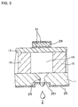
- FIG. 2 The structure of the head of the ink-jet device used in the manufacturing method of the organic EL element according to the present invention is shown in Fig. 2.
- the head 10 for the ink-jet device is provided with, for example, a stainless steel nozzle plate 11 and a vibration plate 13, and they are coupled via partitioning members (reservoir plates) 15.
- a liquid storage 21 and a plurality of spaces 19 are formed by means of the reservoir plates 15.
- the inside of the respective spaces 19 and the liquid storage 21 are filled with the composition according to the present invention, and the spaces 19 communicate with the liquid storage 21 by means of supply ports 23.
- a nozzle hole 25 is provided in the nozzle plate 11 for discharging the composition in a jet-form from the spaces 19.
- a hole 27 is formed in the vibration plate 13 for supplying the composition to the liquid storage 21.
- piezoelectric elements 29 are attached at positions corresponding to the positions of the respective spaces 19.
- the piezoelectric element 29 When the piezoelectric element 29 is energized, the piezoelectric element 29 and the vibration plate 13 are deformed, by which the volume of the space 19 is changed, so that the material for the thin film is discharged from the nozzle hole 25 toward the substrate.
- a water repellent treatment such as Teflon coating treatment or the like are made at the inner wall portion of the nozzle hole 25 and its peripheral part in order to prevent the bend in the jetted direction of the composition and prevent clogging of the hole by the composition.
- organic EL luminescent layers respectively by discharging the compositions corresponding to, for example, the three primary colors red, blue, and green according to predetermined patterns, thereby enabling to form the pixels.
- the amount of the composition to be discharged, the number of times of the discharge and the forms of patterns can be adjusted easily and handily, so that the luminescent characteristics and film thickness and the like of the luminescent layers can be controlled.
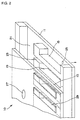
- Fig. 1 is a sectional view which shows steps performed in the embodiment of the manufacturing method for an organic EL element of the present invention.
- pixel electrodes 101, 102 and 103 are formed on a transparent substrate 104 such as a substrate made of glass.
- a transparent substrate 104 such as a substrate made of glass.
- photolithography, vacuum deposition method, sputtering method and pyrosol method can be mentioned.
- These pixel electrodes are preferably transparent.
- a tin oxide film, an ITO (indium tin oxide) film and a composite oxide film of indium oxide and zinc oxide can be mentioned.
- red, green and blue compositions After coating and patterning red, green and blue compositions by jetting the above-mentioned compositions from the head 110 of the ink-jet device 109, they are undergone heat treatment under a nitrogen atmosphere to conjugate the precursors in the compositions, thereby forming luminescent layers 106 (red), 107 (green) and 108 (blue) in the form of patterns.
- an electron injection and transfer layer 111 is laminated on the luminescent layers 106, 107 and 108.
- the electron injection and transfer layer 111 facilitates the injection of the electrons from the cathode, and contributes to the prevention of electrode quenching by keeping the luminescent portions away from the cathode to establish a better contact with the cathode.
- the electron injection and transfer layer 111 aluminum quinolynol complex to which the doping is not carried out can be used.
- oxadiazole derivatives such as PBD, OXD-8 and the like; DSA; Bebq; triazole derivative; azomethine complex; porphyrin complex; benzoxadiazol complex; and the like can be mentioned.
- the electron injection and transfer layer may be formed by using any one of these compounds, or mixing or laminating two or more of these compounds.
- the forming method for the electron injection and transfer layer 111 is not limited to a specific method. It is possible to form the electron injection and transfer layer 111 by using, for example, ink-jet method, vacuum deposition method, dipping method, spin coating method, casting method, capillary method, roll coating method, bar coating method or the like.
- the cathode 113 is formed into a metallic thin film electrode.
- the metal for forming the cathode Mg, Ag, Al, Li and the like can be mentioned.
- a material having small work function can be used for the material for the cathode 113.
- alkali metal, alkali earth metal such as Ca and the like, and alloys containing these metals can be used.
- the cathode 113 may be formed by using, for example, deposition method, sputtering method or the like.
- Fig. 5 is a sectional view which shows a process of another embodiment of the manufacturing method for an organic EL element according to the present invention.
- pixel electrodes 101, 102 and 103 are formed on a transparent substrate 104 such as a glass substrate, and then banks 105 are formed by means of photolithography.
- compositions are jetted out from a head 110 for an ink-jet device 109 so that the patterns of compositions for various colors are coated and formed onto the pixel electrodes 101, 102 and 103.
- a blue luminescent layer 108 is formed on the red luminescent layer 106, the green luminescent layer 107 and the pixel electrode 103.
- the forming method for the blue luminescent layer 108 No particular limitation is imposed upon the forming method for the blue luminescent layer 108. It is possible to form the layer using the general film forming method known as deposition method or wet method, for instance, or using the ink-jet method.
- the blue luminescent layer 108 can be formed of an electron injection and transfer material such as aluminum quinolynol complex. With a structure such as this, it is possible to promote the injection and transfer of the carriers so as to improve the luminous efficiency.
- a blue luminescent layer 108 is laminated with a luminescent layer formed of a hole injection and transfer material such as, for example, PPV layer or the like, it is also possible to inject and transfer efficiently the electrons and the holes from the respective electrodes into these laminated luminescent layers, thereby enabling to more improve the luminous efficiency.
- a hole injection and transfer material such as, for example, PPV layer or the like
- the function of hole injection and transfer and the function of electron injection and transfer can be assigned separately to different layers, so that optimum design can be selected for the respective materials.
- the luminescent layer for the other color may be formed by a different method. Therefore, even when a luminescent material which is not so suited for the ink-jet method is used, a full color organic EL element can be formed by using such a material in a combination with other organic luminescent materials that are suited for the ink-jet method, so that the latitude in the design for the EL element will be expanded.
- the forming method used for the formation of the luminescent layer other than the ink-jet method photolithography method, vacuum deposition method, printing method, transfer method, dipping method, spin coating method, casting method, capillary method, bar coating method, roll coating method and the like can be mentioned.
- composition for an organic EL element and the method of manufacturing an organic EL element according to the present invention are described in details with reference to the actual examples.
- compositions for the organic EL element made from the compositions shown in Table 1 were prepared for respective colors, and then the organic EL element was manufactured using the compositions.
- ITO transparent pixel electrodes 101, 102 and 103 were formed by means of photolithography so as to form respectively a pattern having a pitch of 100 ⁇ m and a thickness of 0.1 ⁇ m.
- each of the banks 105 was designed so as to have a width of 20 ⁇ m and a thickness of 2.0 ⁇ m, respectively.
- the luminescent materials for the respective colors were coated to form patterns by jetting the compositions from the head 110 of the ink-jet device 109. Then, they were undergone heat treatment under a nitrogen atmosphere at 150°C for 4 hours to conjugate the precursors in the compositions of the materials so as to obtain thin films, thereby obtaining luminescent layers 106 (red), 107 (green) and 108 (blue) which emit red, green and blue, respectively.
- the vacuum deposition was carried out using the aluminum quinolynol complex to which no doping was carried out to form an electron injection and transfer layer 111 having a thickness of 0.1 ⁇ m.
- an Al - Li electrode having a thickness of 0.8 ⁇ m was formed as the cathode 113 by the deposition method, thereby manufacturing the organic EL element.
- the organic EL element was manufactured in the same way as Example 1 except that quinacridone of 0.075 wt% (ratio for solid portion of PPV precursor: 2wt % ) was added into the green luminescent layer composition as a fluorescent dye as shown in Table 2.
- the organic EL element was manufactured in the same way as Example 1 except that rhodamine 101 was used as a fluorescent dye in the red luminescent layer composition as shown in Table 3,
- the organic EL element was manufactured in the same way as Example 1 except that coumarin 6 of 0.00375wt % and distyrylbiphenyl of 0.00375wt % (ratio for solid portion of PPV precursor: 1wt %) were used as a fluorescent dye in the blue luminescent layer composition and that glycerin of 3wt % and diethylene glycol of 12wt% were used as a wetting agent as shown in Table 4.
- the organic EL element was manufactured in the same way as Example 1 except that tetraphenylbutadiene (TPB) of 0.0075wt % (ratio for solid portion of PPV precursor: 2wt %) was used as a fluorescent dye in the blue luminescent layer composition and quinacridone of 0.0075wt % (ratio for solid portion of PPV precursor: 2wt %) was used as a fluorescent dye in the green luminescent layer composition, respectively, and that glycerin of 3wt% and diethylene glycol of 12wt% were used as a wetting agent as shown in Table 5.
- TPB tetraphenylbutadiene
- the organic EL element was manufactured in the same way as Example 1 except that coumarin 138 was used in the blue luminescent layer composition as a fluorescent dye as shown in Table 6.
- the organic EL element was manufactured in the same way as Example 1 except that CN-PPV precursor which emits red color was used instead of PPV precursor and that distyrylbiphenyl of 0.0075wt% (ratio for solid portion of PPV precursor: 2wt%) was used as a blue fluorescent dye and quinacridone of 0.0075wt % (ratio for solid portion of PPV precursor: 2wt %) was used as a green fluorescent dye without adding any red fluorescent dye, as shown in Table 7.
- Alq 3 aluminum quinolynol complex
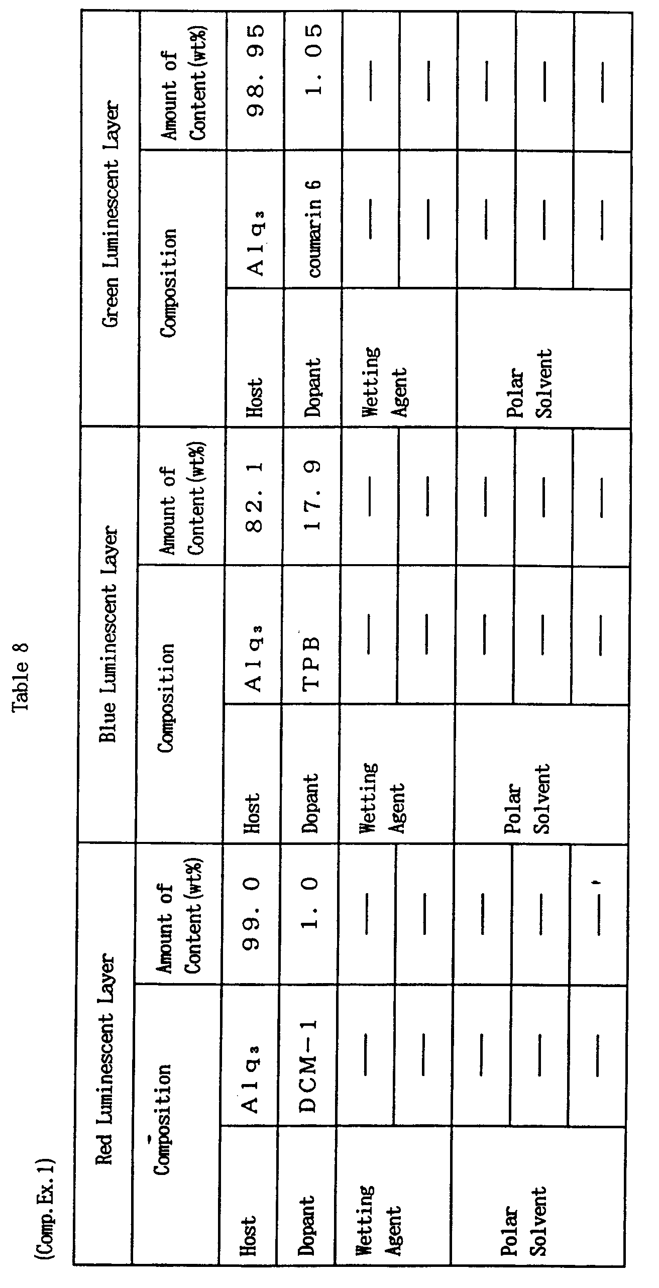
- compositions for an EL element were prepared, in which aluminum quinolynol complex (Alq 3 ) was added as a host material, DCM-1 (red), TPB (blue) and coumarin 6 (green) were added to the respective compositions as a dopant, and wetting agent and polar solvent were also contained. Then, respective luminescent layers were formed by the ink-jet method using the compositions in the same way as Example 1 to obtain an organic EL element.
- Alq 3 aluminum quinolynol complex
- a prescribed voltage was applied to the element, and the applied voltage at which a luminance of 1 cd/m 2 is observed was defined as the luminescence starting voltage [Vth].
- the initial luminance after a stabilization treatment has been carried out was set to 100%, and the changes in the luminance of the EL element were measured under the condition that the elements were kept in continuous luminescence by supplying a constant current of standard waveform, wherein the luminescence life is defined as the time until the luminance drops to 50% of the initial luminance.
- the drive conditions for this experiment were set at 40°C for room temperature, 23% for humidity and 20 mA/cm 2 for current density.
- the luminance was measured at which the current was set to 20 mA/cm 2 .
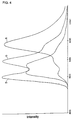
- Fig. 4 is a diagram which shows wavelength at absorption of light at the each luminescent layers of the organic EL element in Example 1. As the result of measuring the wavelength at maximum absorption for the respective luminescent layers of the organic EL elements obtained in Examples 2 to 7, the same results were obtained,
- the luminescent layers in Examples 1 to 7 have excellent luminescence characteristics and excellent film characteristics
- a composition for the organic EL element having compositions shown in Table 12 was prepared, and then the composition for the organic EL element was discharged from the nozzle of the ink-jet device in the same way as Example 1 to carry out the coating and the pattern formation.
- the blue luminescent layer was formed in the same way as Example 8 except that distyrylbiphenyl was used as a blue fluorescent dye instead of the rhodamine B as shown in Table 13.
- the green luminescent layer was formed in the same way as Example 8 except that quinacridone was used as a green fluorescent dye instead of the rhodamine B as shown in Table 14.
- the blue luminescent layer was formed in the same way as Example 8 except that coumarin 6 was used as a blue fluorescent dye instead of the rhodamine B and that the amount of glycerin and diethylene glycol to be added as a wetting agent was changed as shown in Table 15.
- the blue luminescent layer was formed in the same way as Example 8 except that TPB (tetraphenylbutadiene) was used as a blue fluorescent dye instead of the rhodamine as shown in Table 16.
- TPB tetraphenylbutadiene
- the green luminescent layer was formed in the same way as Example 8 except that CN-PPV precursor which emits red color was used instead of PPV precursor, and that quinacridone of 0.0075 wt% was added as a green fluorescent dye as shown in Table 17.
- the green luminescent layer was formed in the same way as Example 8 except that a composition which includes aqueous solution of PPV precursor of 50wt % ; glycerin of 20wt % and diethylene glycol of 20 wt% for wetting agents; and DMF of 10 wt % for polar solvent; and quinacridone as a green fluorescent dye instead of the rhodamine B were used, as shown in Table 18.
- the blue luminescent layer was formed in the same way as Example 8 except that coumarin 6 was used as a blue fluorescent dye instead of rhodamine B, that DMF of 75wt % was used as a polar solvent, and that no wetting agent was added, as shown in Table 19.
- the red luminescent layer was formed in the same way as Example 8 except that a composition which includes aqueous solution of PPV precursor of 50wt % ; glycerin of 10wt % and diethylene glycol of 10wt% for wetting agents; and DMF of 30wt% for polar solvent was used as shown in Table 20.
- the occurrence frequency of the bend in the jetted direction of the composition and the occurrence frequency of clogging of the nozzle hole at the time of discharging the composition from the nozzle hole of an ink-jet printer (made by EPSON Co., Ltd. Model No. MJ-500C, the material constituting the nozzle surface is a water repellent layer to which eutectic tetrafluoroethylene-nickel is plated) were also investigated.
- the contact angle for each composition with respect to the material constituting the nozzle surface was measured in accordance with the measurement method of the contact angle as stipulated in JIS K3211.
- each of the compositions in Examples 8 to 13 has markedly lower values of the occurrence frequency of the bend in the jetted direction and the occurrence frequency of the clogging of the nozzle hole in comparison with those of Comparative Examples, and the occurrence frequencies indicated by the values were within the range of the practical level.
- the composition in Comparative Example 4 has a large value for the occurrence frequency of the bend in the jetted direction, so that it was found that it is not suitable for fine pattern formation.
- the electron injection and transfer layer 111 having a thickness of 0.1 ⁇ m was laminated on the luminescent layers which were formed of the respective compositions in Examples 8 to 13.
- an Al - Li electrode having a thickness of 0.8 ⁇ m was formed as the cathode 113, respectively, by the deposition method, and thereby manufacturing the organic EL elements.
- the luminescent characteristics and the film properties of the luminescent layers formed from the compositions of Examples 8 to 13 were evaluated by the same methods as described above with reference to the description "2. Evaluation of Luminescent Characteristics and Film Properties of the Luminescent Layer".
- the luminescent characteristics and the film properties of all of the luminescent layers formed using the compositions of Examples 8 to 13 were excellent. Namely, it was possible to obtain organic EL elements free from dark spots and have high luminance and long life.
- the present invention is not limited to these embodiments. Namely, in the method of manufacturing the organic EL element, it may further includes a step of inserting arbitrary intermediate layers such as a carrier transporting layer or a buffer layer between the layers.
- a carrier transporting layer such as a carrier transporting layer or a buffer layer between the layers.
- the buffer layer 1,2,4-triazole (TAZ) derivative and the like can be mentioned, which is effective for improving the luminance and the luminescence life.
- the method may further include a step in which surface treatment such as plasma treatment, UV treatment, coupling or the like are applied to surfaces of pixel electrode, an underlying layer and the like in order to facilitate the sticking of the EL materials. Further, the method may further include a step of forming a protective layer on the cathode.
- the material constituting the nozzle surface of the ink-jet device is not limited to those of the embodiments described above.
- the fluorescent dye to be added for changing the luminescent characteristics is not limited to those of the embodiments as long as they can be dissolved and dispersed homogeneously into a solvent.
- compositions for the organic EL element of the present invention a rational design of the organic EL element is possible through wide ranging selection of luminescent materials.
- the composition for the organic EL element includes a precursor of a conjugated polymer based organic compound and a fluorescent dye, it is possible to manufacture an organic EL element which realizes a full color display since various kinds of luminescent layers can be obtained through the selection of various materials.
- conditions for a composition such as contact angle, viscosity and surface tension can be freely set, the conditions suitable as a discharge liquid for the ink-jet method can be easily adjusted.
- the method of manufacturing the organic EL element it is possible to employ the ink-jet method to the formation of a luminescent layer, a hole injection and transfer layer, and an electron injection and transfer layer. In that case, it is possible to carry out easily a high precise pattern formation in a short time without the occurrence of the bend in the jetted direction of a discharge liquid and the occurrence of the clogging of the nozzle hole.
- the optimizations of the film design and the luminescent characteristics can be readily achieved, thereby enabling to form a luminescent layer and an EL layer which are capable of easy adjustment of luminescence efficiency and have excellent durability.
- conditions such as the film thickness, the number of dots and the like can be adjusted arbitrarily, so that the size and the pattern of the luminescent element can also be set arbitrarily.
- the element can be formed without being restrained by the dimensions of the substrate and the like since the head can be moved freely. Moreover, since required amounts of materials can be arranged at required locations, it is possible to maximally exclude the uselessness of waste liquid and the like.
- composition for the organic EL element according to the present invention is not limited to the embodiments described above, and it is possible to make various changes and additions without departing from the scope and spirit of the present invention as defined in the appended claims.
Abstract
Description


Claims (31)
- A composition for an organic EL element for forming at least one luminescent layer having a certain color, said composition comprising;a precursor of a conjugated organic polymer compound for forming said luminescent layer; andat least one kind of fluorescent dye for changing the luminescence characteristic of the luminescent layer.
- The composition for an organic EL element as claimed in claim 1, wherein said luminescent layer is formed from a pattern of the composition which is formed by an ink-jet method.
- The composition for an organic EL element as claimed in claim 1, wherein the luminescence characteristic is a maximum wavelength of light absorption.
- The composition for an organic EL element as claimed in claim 1, wherein the conjugated organic polymer compound is a hole injection and transfer type material.
- The composition for an organic EL element as claimed in claim 1, wherein the precursor of the conjugated organic polymer compound includes a polyallylene vinylene precursor.
- The composition for an organic EL element as claimed in claim 5, wherein the precursor of the conjugated organic polymer compound includes a precursor of a polyparaphenylene vinylene or a polyparaphenylene vinylene derivative.
- The composition for an organic EL element as claimed in claim 1, wherein the fluorescent dye includes rhodamine or rhodamine derivative.
- The composition for an organic EL element as claimed in claim 1, wherein the fluorescent dye includes distyrylbiphenyl or distyrylbiphenyl derivative.
- The composition for an organic EL element as claimed in claim 1, wherein the fluorescent dye includes coumarin or coumarin derivative.
- The composition for an organic EL element as claimed in claim 1, wherein the fluorescent dye includes tetraphenylbutadiene (TPB) or tetraphenylbutadiene derivative.
- The composition for an organic EL element as claimed in claim 1, wherein the fluorescent dye includes quinacridone or quinacridone derivative.
- The composition for an organic EL element as claimed in claim 1, wherein the precursor of the conjugated organic polymer compound and the fluorescent dye exist in the state of being dissolved or dispersed into a polar solvent.
- The composition for an organic EL element as claimed in claim 1, wherein the amount of the fluorescent dye to be added is 0.5 to 10wt% with respect to a solid component of the precursor of the conjugated organic polymer compound.
- The composition for an organic EL element as claimed in claim 1, wherein the composition contains a wetting agent for preventing the composition from being dried and solidified.
- The composition for an organic EL element as claimed in claim 2, wherein a contact angle with respect to a material constituting a nozzle surface of a nozzle provided in a head of an ink-jet device used for the ink-jet method for discharging the composition lies in the range of 30 to 170 degrees.
- The composition for the organic EL element as claimed in claim 1, wherein a viscosity of the composition for the organic EL element is 1 to 20cp.
- The composition for the organic EL element as claimed in claim 1, wherein a surface tension of the composition for the organic EL element is 20 to 70dyne/cm.
- A method of manufacturing an organic EL element, comprising the steps of:coating a pattern by discharging a composition for an organic EL element containing a precursor of a conjugated organic polymer compound from a head by an ink-jet method; andforming at least one luminescent layer for a certain color by conjugating the precursor of the conjugated organic polymer compound.
- The method of manufacturing the organic EL element as claimed in claim 18, wherein the composition further comprises at least one kind of luminescent dye for changing a luminescence characteristic of the luminescent layer.
- The method of manufacturing the organic EL element as claimed in claim 19, wherein the luminescence characteristic is a maximum wavelength of light absorption.
- The method of manufacturing the organic EL element as claimed in claim 18, wherein the conjugated organic polymer compound is a hole injection and transfer type material.
- The method of manufacturing the organic EL element as claimed in claim 18, wherein the precursor of the conjugated organic polymer compound includes a precursor of a polyallylene vinylene.
- The method of manufacturing the organic EL element as claimed in claim 22, wherein the precursor of the polyallylene vinylene includes a precursor of a polyparaphenylene vinylene or a polyparaphenylene vinylene derivative.
- The method of manufacturing the organic EL element as claimed in any one of claims 19, wherein the fluorescent dye includes rhodamine or rhodamine derivative.
- The method of manufacturing the organic EL element as claimed in claim 19, wherein the fluorescent dye includes distyrylbiphenyl or distyrylbiphenyl derivative.
- The method of manufacturing the organic EL element as claimed in claim 19, wherein the fluorescent dye includes coumarin or coumarin derivative.
- The method of manufacturing the organic EL element as claimed in claim 19, wherein the fluorescent dye includes tetraphenylbutadiene (TPB) or tetraphenylbutadiene derivative.
- The method of manufacturing the organic EL element as claimed in claim 19, wherein the fluorescent dye includes quinacridone or quinacridone derivative.
- The method of manufacturing the organic EL element as claimed in claim 18, wherein a contact angle with respect to a material constituting a nozzle surface of a nozzle of a device used for the ink-jet method for discharging the composition lies in the rage of 30 to 170degrees.
- The method of manufacturing the organic EL element as claimed in claim 18, wherein a viscosity of the composition for the organic EL element is 1 to 20cp.
- The method of manufacturing the organic EL element as claimed in 18, wherein a surface tension of the composition for the organic EL element is 20 to 70dyne/cm.
Priority Applications (1)
| Application Number | Priority Date | Filing Date | Title |
|---|---|---|---|
| EP03025785A EP1394236B1 (en) | 1997-07-16 | 1998-07-14 | Composition for an organic EL element |
Applications Claiming Priority (6)
| Application Number | Priority Date | Filing Date | Title |
|---|---|---|---|
| JP19168197 | 1997-07-16 | ||
| JP191681/97 | 1997-07-16 | ||
| JP19168197A JP3941169B2 (en) | 1997-07-16 | 1997-07-16 | Manufacturing method of organic EL element |
| JP20469797A JP3911775B2 (en) | 1997-07-30 | 1997-07-30 | Manufacturing method of organic EL element |
| JP20469797 | 1997-07-30 | ||
| JP204697/97 | 1997-07-30 |
Related Child Applications (1)
| Application Number | Title | Priority Date | Filing Date |
|---|---|---|---|
| EP03025785A Division EP1394236B1 (en) | 1997-07-16 | 1998-07-14 | Composition for an organic EL element |
Publications (3)
| Publication Number | Publication Date |
|---|---|
| EP0892028A2 true EP0892028A2 (en) | 1999-01-20 |
| EP0892028A3 EP0892028A3 (en) | 1999-02-03 |
| EP0892028B1 EP0892028B1 (en) | 2004-02-11 |
Family
ID=26506843
Family Applications (2)
| Application Number | Title | Priority Date | Filing Date |
|---|---|---|---|
| EP03025785A Expired - Lifetime EP1394236B1 (en) | 1997-07-16 | 1998-07-14 | Composition for an organic EL element |
| EP98113051A Expired - Lifetime EP0892028B1 (en) | 1997-07-16 | 1998-07-14 | Composition for an organic EL element and method of manufacturing the organic EL element |
Family Applications Before (1)
| Application Number | Title | Priority Date | Filing Date |
|---|---|---|---|
| EP03025785A Expired - Lifetime EP1394236B1 (en) | 1997-07-16 | 1998-07-14 | Composition for an organic EL element |
Country Status (6)
| Country | Link |
|---|---|
| US (2) | US6843937B1 (en) |
| EP (2) | EP1394236B1 (en) |
| KR (1) | KR100554338B1 (en) |
| CN (1) | CN1244002C (en) |
| DE (2) | DE69838402T2 (en) |
| TW (1) | TW417031B (en) |
Cited By (45)
| Publication number | Priority date | Publication date | Assignee | Title |
|---|---|---|---|---|
| EP1029369A1 (en) * | 1997-10-17 | 2000-08-23 | The Regents Of The University Of California | Process for fabricating organic semiconductor devices using ink-jet printing technology and device and system employing same |
| EP1030383A2 (en) * | 1999-02-16 | 2000-08-23 | Sharp Kabushiki Kaisha | Charge-transport structures |
| WO2001006577A1 (en) * | 1999-07-20 | 2001-01-25 | Sri International | Cavity-emission electroluminescent device and method for forming the device |
| WO2001047045A1 (en) * | 1999-12-21 | 2001-06-28 | Plastic Logic Limited | Solution processing |
| EP1128449A2 (en) | 2000-02-28 | 2001-08-29 | Semiconductor Energy Laboratory Co., Ltd. | Thin film forming method for light emitting devices |
| US6420200B1 (en) | 1999-06-28 | 2002-07-16 | Semiconductor Energy Laboratory Co., Ltd. | Method of manufacturing an electro-optical device |
| US6440877B1 (en) | 1999-06-28 | 2002-08-27 | Semiconductor Energy Laboratory Co., Ltd. | Method of manufacturing an electro-optical device |
| GB2373095A (en) * | 2001-03-09 | 2002-09-11 | Seiko Epson Corp | Patterning substrates with evaporation residues |
| GB2330451B (en) * | 1997-10-14 | 2002-11-20 | Thin Film Technology | Method of forming an electronic device |
| WO2002101846A2 (en) * | 2001-06-12 | 2002-12-19 | Koninklijke Philips Electronics N.V. | (electro)luminescent polymer-acceptor system comprising a polymer and an acceptor for transferring excitation energy |
| WO2002100975A2 (en) * | 2001-06-12 | 2002-12-19 | Koninklijke Philips Electronics N.V. | (electro)luminescent device with an organic dye as an acceptor |
| WO2003007377A2 (en) * | 2001-07-11 | 2003-01-23 | Osram Opto Semiconductors Gmbh | Organic, electroluminescent display and method for producing the same |
| DE10133686A1 (en) * | 2001-07-11 | 2003-01-30 | Osram Opto Semiconductors Gmbh | Organic, electroluminescent display and its manufacture |
| EP1296540A1 (en) * | 2000-06-28 | 2003-03-26 | Toray Industries, Inc. | Display |
| WO2003038922A1 (en) * | 2001-10-26 | 2003-05-08 | Osram Opto Semiconductors Gmbh | Method for applying mechanically sensitive layers to a substrate over a large area |
| DE10157945A1 (en) * | 2001-11-27 | 2003-06-12 | Osram Opto Semiconductors Gmbh | Process for producing an organic, electroluminescent display and an organic, electroluminescent display |
| GB2388709A (en) * | 2002-05-17 | 2003-11-19 | Seiko Epson Corp | Circuit fabrication method |
| US6656611B2 (en) | 2001-07-20 | 2003-12-02 | Osram Opto Semiconductors Gmbh | Structure-defining material for OLEDs |
| US6699739B2 (en) | 2000-03-06 | 2004-03-02 | Semiconductor Energy Laboratory Co., Ltd. | Thin film forming device, method of forming a thin, and self-light-emitting device |
| WO2004023574A1 (en) * | 2002-09-06 | 2004-03-18 | E.I. Du Pont De Nemours And Company | Methods for producing full-color organic electroluminescent devices |
| US6781746B2 (en) | 2000-03-27 | 2004-08-24 | Semiconductor Energy Laboratory Co., Ltd. | Self-light emitting device and method of manufacturing the same |
| US6887392B2 (en) | 2001-06-25 | 2005-05-03 | Semiconductor Energy Laboratory Co., Ltd. | Light emitting device and method of manufacturing the same |
| WO2005051049A1 (en) * | 2003-11-21 | 2005-06-02 | Koninklijke Philips Electronics N.V. | Display panel |
| US6939732B2 (en) | 2001-07-11 | 2005-09-06 | Osram Opto Semiconductors Gmbh | Organic, colored, electroluminescent display and the production thereof |
| US6956645B2 (en) | 2001-12-21 | 2005-10-18 | Osram Opto Semiconductors Gmbh | Apparatus and method for in-situ measurement of polymer quantities output from an extractor |
| US7084236B2 (en) | 2001-05-29 | 2006-08-01 | Koninklijke Philips Electronics N.V. | Polymer, method of its preparation, and electronic device |
| US7115434B2 (en) | 1999-10-13 | 2006-10-03 | Semiconductor Energy Laboratory Co., Ltd. | Method for precisely forming light emitting layers in a semiconductor device |
| US7198814B2 (en) * | 2001-03-12 | 2007-04-03 | Seiko Epson Corporation | Compositions, methods for producing films, functional elements, methods for producing functional elements, method for producing electro-optical devices and methods for producing electronic apparatus |
| US7204735B2 (en) | 2002-07-09 | 2007-04-17 | Semiconductor Energy Laboratory Co., Ltd. | Production apparatus and method of producing a light-emitting device by using the same apparatus |
| US7279194B2 (en) | 2000-02-04 | 2007-10-09 | Semiconductor Energy Laboratory Co., Ltd. | Thin film formation apparatus and method of manufacturing self-light-emitting device using thin film formation apparatus |
| WO2008059264A1 (en) * | 2006-11-15 | 2008-05-22 | Cambridge Display Technology Limited | Droplet deposition method |
| US7462372B2 (en) | 2000-09-08 | 2008-12-09 | Semiconductor Energy Laboratory Co., Ltd. | Light emitting device, method of manufacturing the same, and thin film forming apparatus |
| US20080305245A1 (en) * | 1999-03-29 | 2008-12-11 | Cambridge Display Technology Limited | Composition, film manufacturing method, as well as functional device and manufacturing method therefor |
| US7485584B2 (en) | 2001-05-21 | 2009-02-03 | Semiconductor Energy Laboratory Co., Ltd. | Light emitting device and method of manufacturing thereof |
| US7547562B2 (en) | 2001-08-29 | 2009-06-16 | Semiconductor Energy Laboratory Co., Ltd. | Light emitting device and method for manufacturing same |
| US7745991B2 (en) | 1999-10-12 | 2010-06-29 | Semiconductor Energy Laboratory Co., Ltd. | Electro-optical device having an EL layer over a plurality of pixels |
| EP2219420A1 (en) * | 2007-11-30 | 2010-08-18 | Sumitomo Chemical Company, Limited | Electronic device, display apparatus and method for manufacturing electronic device |
| US8022614B2 (en) | 2004-12-16 | 2011-09-20 | Koninklijke Philips Electronics N.V. | Display panel and method for manufacturing the same |
| US8119188B2 (en) | 2001-06-08 | 2012-02-21 | Semiconductor Energy Laboratory Co., Ltd. | Process of manufacturing luminescent device |
| US8133748B2 (en) | 1999-10-12 | 2012-03-13 | Semiconductor Energy Laboratory Co., Ltd. | EL display device and method of manufacturing the same |
| US8383841B2 (en) | 2003-05-09 | 2013-02-26 | Applied Biosystems, Llc | Phenyl xanthene dyes |
| US8574937B2 (en) | 2008-01-24 | 2013-11-05 | Sri International | High efficiency electroluminescent devices and methods for producing the same |
| US8618161B2 (en) | 2003-05-09 | 2013-12-31 | Applied Biosystems, Llc | Fluorescent polymeric materials containing lipid soluble rhodamine dyes |
| US8697254B2 (en) | 2006-11-14 | 2014-04-15 | Sri International | Cavity electroluminescent devices and methods for producing the same |
| US9133389B2 (en) | 2012-10-31 | 2015-09-15 | Empire Technology Development Llc | Light guide structure and illuminating device |
Families Citing this family (27)
| Publication number | Priority date | Publication date | Assignee | Title |
|---|---|---|---|---|
| JP2002215065A (en) * | 2000-11-02 | 2002-07-31 | Seiko Epson Corp | Organo-electroluminescence device and its manufacturing method and electronic equipment |
| JP3953776B2 (en) | 2001-01-15 | 2007-08-08 | セイコーエプソン株式会社 | Material discharging apparatus and method, color filter manufacturing apparatus and manufacturing method, liquid crystal device manufacturing apparatus and manufacturing method, EL apparatus manufacturing apparatus and manufacturing method |
| JP2003022892A (en) * | 2001-07-06 | 2003-01-24 | Semiconductor Energy Lab Co Ltd | Manufacturing method of light emitting device |
| US6921148B2 (en) | 2002-01-30 | 2005-07-26 | Seiko Epson Corporation | Liquid drop discharge head, discharge method and discharge device; electro optical device, method of manufacture thereof, and device for manufacture thereof; color filter, method of manufacture thereof, and device for manufacture thereof; and device incorporating backing, method of manufacture thereof, and device for manufacture thereof |
| US6858464B2 (en) | 2002-06-19 | 2005-02-22 | Semiconductor Energy Laboratory Co., Ltd. | Method of manufacturing light emitting device |
| JP4405137B2 (en) * | 2002-07-12 | 2010-01-27 | 大日本スクリーン製造株式会社 | Coating device |
| TWI300669B (en) * | 2002-07-12 | 2008-09-01 | Dainippon Screen Mfg | Apparatus and method of coating organic electroluminescence material |
| CN101694871B (en) | 2002-11-11 | 2012-12-05 | 株式会社半导体能源研究所 | Process for fabricating light emitting device |
| JP4378950B2 (en) * | 2002-12-24 | 2009-12-09 | セイコーエプソン株式会社 | Droplet ejection apparatus and electro-optic device manufacturing method |
| JP3966283B2 (en) * | 2003-01-28 | 2007-08-29 | セイコーエプソン株式会社 | LIGHT EMITTING BODY, ITS MANUFACTURING METHOD AND DEVICE, ELECTRO-OPTICAL DEVICE, AND ELECTRONIC DEVICE |
| KR100663028B1 (en) * | 2003-12-30 | 2006-12-28 | 엘지.필립스 엘시디 주식회사 | Organic Electro Luminescence Device and the fabrication method of thereof |
| JP4195411B2 (en) * | 2004-04-12 | 2008-12-10 | セイコーエプソン株式会社 | Method for manufacturing organic electroluminescence device |
| JP4616596B2 (en) * | 2004-08-27 | 2011-01-19 | 株式会社 日立ディスプレイズ | Manufacturing method of electronic device |
| US20060099445A1 (en) * | 2004-11-08 | 2006-05-11 | Wintek Corporation | Organic electro-luminescence device and method of making the same |
| CN100450774C (en) * | 2004-11-08 | 2009-01-14 | 精工爱普生株式会社 | Droplet ejection method, electro-optic device manufacturing method, and electronic instrument |
| US7268006B2 (en) | 2004-12-30 | 2007-09-11 | E.I. Du Pont De Nemours And Company | Electronic device including a guest material within a layer and a process for forming the same |
| US20060214577A1 (en) * | 2005-03-26 | 2006-09-28 | Lorraine Byrne | Depositing of powdered luminescent material onto substrate of electroluminescent lamp |
| JP5065276B2 (en) * | 2005-09-05 | 2012-10-31 | オスラム オプト セミコンダクターズ ゲゼルシャフト ミット ベシュレンクテル ハフツング | Novel materials for n-type doping of electron transport layers in organic electronic devices |
| TW200740955A (en) * | 2006-04-20 | 2007-11-01 | Wintek Corp | Organic electroluminescent device |
| CN101381438B (en) * | 2007-09-05 | 2013-06-26 | 北京同创海诚科技发展有限公司 | Compound material constructed by molecular engram and fluorescent conjugated polymer, preparation and application |
| US20090311799A1 (en) * | 2008-06-13 | 2009-12-17 | Sotzing Gregory A | Nucleic Acid Materials for Nonradiative Energy Transfer and Methods of Production and Use |
| US20100288343A1 (en) * | 2009-05-18 | 2010-11-18 | University Of Connecticut | Nucleic acid-based photovoltaic cell |
| DE102012016759A1 (en) * | 2012-08-27 | 2014-02-27 | Inoviscoat Gmbh | Luminous element having a luminescent layer which has electroluminescent particles |
| ES2648364T3 (en) | 2011-12-19 | 2018-01-02 | Inoviscoat Gmbh | Luminous elements with an electroluminescent arrangement as well as a procedure for the production of a luminous element |
| KR102114314B1 (en) * | 2013-06-26 | 2020-05-25 | 삼성디스플레이 주식회사 | Organic light emitting display device and method for manufacturing the same |
| JP6638187B2 (en) | 2014-12-02 | 2020-01-29 | セイコーエプソン株式会社 | Film forming ink and film forming method |
| JP6638186B2 (en) | 2014-12-02 | 2020-01-29 | セイコーエプソン株式会社 | Film forming ink and film forming method |
Citations (4)
| Publication number | Priority date | Publication date | Assignee | Title |
|---|---|---|---|---|
| WO1990013148A1 (en) * | 1989-04-20 | 1990-11-01 | Cambridge Research And Innovation Limited | Electroluminescent devices |
| WO1995001871A1 (en) * | 1993-07-09 | 1995-01-19 | The Regents Of The University Of California | Electroluminescent diodes utilizing blends of polymers |
| EP0756932A2 (en) * | 1995-07-31 | 1997-02-05 | Canon Kabushiki Kaisha | Color-filter manufacturing method and apparatus, color filter, display device, and apparatus having display device |
| US5665857A (en) * | 1994-09-12 | 1997-09-09 | Motorola | Conjugated polymer with built-in fluorescent centers and method of manufacture |
Family Cites Families (24)
| Publication number | Priority date | Publication date | Assignee | Title |
|---|---|---|---|---|
| US4822718A (en) * | 1982-09-30 | 1989-04-18 | Brewer Science, Inc. | Light absorbing coating |
| US4533569A (en) * | 1983-12-08 | 1985-08-06 | Ncr Corporation | Process preventing air bubble lock in ink jet nozzles |
| JPS6231174A (en) | 1985-08-02 | 1987-02-10 | Mitsubishi Electric Corp | Field effect transistor |
| JPH0711631B2 (en) | 1985-10-09 | 1995-02-08 | 三菱電機株式会社 | Liquid crystal display manufacturing method |
| US5132248A (en) | 1988-05-31 | 1992-07-21 | The United States Of America As Represented By The United States Department Of Energy | Direct write with microelectronic circuit fabrication |
| DE69110922T2 (en) * | 1990-02-23 | 1995-12-07 | Sumitomo Chemical Co | Organic electroluminescent device. |
| JP3069139B2 (en) * | 1990-03-16 | 2000-07-24 | 旭化成工業株式会社 | Dispersion type electroluminescent device |
| US5326692B1 (en) | 1992-05-13 | 1996-04-30 | Molecular Probes Inc | Fluorescent microparticles with controllable enhanced stokes shift |
| US5730922A (en) * | 1990-12-10 | 1998-03-24 | The Dow Chemical Company | Resin transfer molding process for composites |
| US5214350A (en) | 1991-09-11 | 1993-05-25 | Zenith Electronics | Identification of image displays and their component parts |
| US5276380A (en) | 1991-12-30 | 1994-01-04 | Eastman Kodak Company | Organic electroluminescent image display device |
| GB9226475D0 (en) | 1992-12-18 | 1993-02-10 | Cambridge Display Tech Ltd | Chromophoric polymeric compositions |
| JP3534445B2 (en) * | 1993-09-09 | 2004-06-07 | 隆一 山本 | EL device using polythiophene |
| US5682043A (en) * | 1994-06-28 | 1997-10-28 | Uniax Corporation | Electrochemical light-emitting devices |
| JP3246189B2 (en) | 1994-06-28 | 2002-01-15 | 株式会社日立製作所 | Semiconductor display device |
| US5610932A (en) | 1995-01-25 | 1997-03-11 | Physical Sciences, Inc. | Solid state dye laser host |
| TW334474B (en) * | 1995-02-01 | 1998-06-21 | Sumitomo Kagaku Kk | Method for making a polymeric fluorescent substrate and organic electrolumninescent element |
| US5593788A (en) | 1996-04-25 | 1997-01-14 | Eastman Kodak Company | Organic electroluminescent devices with high operational stability |
| JPH09123513A (en) * | 1995-11-06 | 1997-05-13 | Fuji Xerox Co Ltd | Conductive polymer thin film and manufacture thereof, driving method for the conductive polymer thin film, method and apparatus for image forming |
| EP0883975B1 (en) * | 1996-07-16 | 2002-10-30 | Koninklijke Philips Electronics N.V. | Organic electroluminescent device |
| JP3899566B2 (en) * | 1996-11-25 | 2007-03-28 | セイコーエプソン株式会社 | Manufacturing method of organic EL display device |
| US6013982A (en) | 1996-12-23 | 2000-01-11 | The Trustees Of Princeton University | Multicolor display devices |
| GB9701680D0 (en) * | 1997-01-28 | 1997-03-19 | Cambridge Display Tech Ltd | Viscosity modification of precursor solutions |
| US6372154B1 (en) * | 1999-12-30 | 2002-04-16 | Canon Kabushiki Kaisha | Luminescent ink for printing of organic luminescent devices |
-
1998
- 1998-07-08 US US09/111,482 patent/US6843937B1/en not_active Expired - Lifetime
- 1998-07-14 EP EP03025785A patent/EP1394236B1/en not_active Expired - Lifetime
- 1998-07-14 DE DE69838402T patent/DE69838402T2/en not_active Expired - Lifetime
- 1998-07-14 EP EP98113051A patent/EP0892028B1/en not_active Expired - Lifetime
- 1998-07-14 DE DE69821554T patent/DE69821554T2/en not_active Expired - Lifetime
- 1998-07-16 TW TW087111559A patent/TW417031B/en not_active IP Right Cessation
- 1998-07-16 CN CNB981172636A patent/CN1244002C/en not_active Expired - Lifetime
-
2004
- 2004-09-22 US US10/946,101 patent/US20050058770A1/en not_active Abandoned
-
2005
- 2005-03-14 KR KR1020050020984A patent/KR100554338B1/en not_active IP Right Cessation
Patent Citations (4)
| Publication number | Priority date | Publication date | Assignee | Title |
|---|---|---|---|---|
| WO1990013148A1 (en) * | 1989-04-20 | 1990-11-01 | Cambridge Research And Innovation Limited | Electroluminescent devices |
| WO1995001871A1 (en) * | 1993-07-09 | 1995-01-19 | The Regents Of The University Of California | Electroluminescent diodes utilizing blends of polymers |
| US5665857A (en) * | 1994-09-12 | 1997-09-09 | Motorola | Conjugated polymer with built-in fluorescent centers and method of manufacture |
| EP0756932A2 (en) * | 1995-07-31 | 1997-02-05 | Canon Kabushiki Kaisha | Color-filter manufacturing method and apparatus, color filter, display device, and apparatus having display device |
Non-Patent Citations (1)
| Title |
|---|
| CHEMICAL ABSTRACTS, vol. 119, no. 16, 18 October 1993 Columbus, Ohio, US; abstract no. 170093, UCHIDA, MASAO ET AL: "Color-variable light-emitting diode utilizing conducting polymer containing fluorescent dye" XP002078807 & JPN. J. APPL. PHYS., PART 2 (1993), 32(7A), L921-L924 CODEN: JAPLD8;ISSN: 0021-4922,1993, * |
Cited By (89)
| Publication number | Priority date | Publication date | Assignee | Title |
|---|---|---|---|---|
| GB2330451B (en) * | 1997-10-14 | 2002-11-20 | Thin Film Technology | Method of forming an electronic device |
| EP1029369A1 (en) * | 1997-10-17 | 2000-08-23 | The Regents Of The University Of California | Process for fabricating organic semiconductor devices using ink-jet printing technology and device and system employing same |
| EP1029369A4 (en) * | 1997-10-17 | 2002-04-03 | Univ California | Process for fabricating organic semiconductor devices using ink-jet printing technology and device and system employing same |
| EP1030383A3 (en) * | 1999-02-16 | 2002-07-17 | Sharp Kabushiki Kaisha | Charge-transport structures |
| EP1030383A2 (en) * | 1999-02-16 | 2000-08-23 | Sharp Kabushiki Kaisha | Charge-transport structures |
| US6555840B1 (en) | 1999-02-16 | 2003-04-29 | Sharp Kabushiki Kaisha | Charge-transport structures |
| US8231932B2 (en) * | 1999-03-29 | 2012-07-31 | Cambridge Display Technology Limited | Composition, film manufacturing method, as well as functional device and manufacturing method therefor |
| US8187669B2 (en) | 1999-03-29 | 2012-05-29 | Seiko Epson Corporation | Composition, film manufacturing method, as well as functional device and manufacturing method therefor |
| US20080305245A1 (en) * | 1999-03-29 | 2008-12-11 | Cambridge Display Technology Limited | Composition, film manufacturing method, as well as functional device and manufacturing method therefor |
| US9620719B2 (en) | 1999-03-29 | 2017-04-11 | Seiko Epson Corporation | Composition, film manufacturing method, as well as functional device and manufacturing method therefor |
| US6420200B1 (en) | 1999-06-28 | 2002-07-16 | Semiconductor Energy Laboratory Co., Ltd. | Method of manufacturing an electro-optical device |
| US6440877B1 (en) | 1999-06-28 | 2002-08-27 | Semiconductor Energy Laboratory Co., Ltd. | Method of manufacturing an electro-optical device |
| US6958251B2 (en) | 1999-06-28 | 2005-10-25 | Semiconductor Energy Laboratory Co., Ltd. | Active matrix display device using a printing method |
| US7342251B2 (en) | 1999-06-28 | 2008-03-11 | Semiconductor Energy Laboratory Co., Ltd. | Method of manufacturing an electro-optical device |
| US6872672B2 (en) | 1999-06-28 | 2005-03-29 | Semiconductor Energy Laboratory Co., Ltd. | Method of manufacturing an electro-optical device |
| US6593687B1 (en) | 1999-07-20 | 2003-07-15 | Sri International | Cavity-emission electroluminescent device and method for forming the device |
| WO2001006577A1 (en) * | 1999-07-20 | 2001-01-25 | Sri International | Cavity-emission electroluminescent device and method for forming the device |
| US8133748B2 (en) | 1999-10-12 | 2012-03-13 | Semiconductor Energy Laboratory Co., Ltd. | EL display device and method of manufacturing the same |
| US8319224B2 (en) | 1999-10-12 | 2012-11-27 | Semiconductor Energy Laboratory Co., Ltd. | EL display device and a method of manufacturing the same |
| US7745991B2 (en) | 1999-10-12 | 2010-06-29 | Semiconductor Energy Laboratory Co., Ltd. | Electro-optical device having an EL layer over a plurality of pixels |
| US8884301B2 (en) | 1999-10-12 | 2014-11-11 | Semiconductor Energy Laboratory Co., Ltd. | EL display device and a method of manufacturing the same |
| US7115434B2 (en) | 1999-10-13 | 2006-10-03 | Semiconductor Energy Laboratory Co., Ltd. | Method for precisely forming light emitting layers in a semiconductor device |
| US7919341B2 (en) | 1999-10-13 | 2011-04-05 | Semiconductor Energy Laboratory Co., Ltd. | Thin film forming apparatus |
| WO2001047045A1 (en) * | 1999-12-21 | 2001-06-28 | Plastic Logic Limited | Solution processing |
| US6808972B2 (en) | 1999-12-21 | 2004-10-26 | Plastic Logic Limited | Method of processing solution on a substrate |
| US7279194B2 (en) | 2000-02-04 | 2007-10-09 | Semiconductor Energy Laboratory Co., Ltd. | Thin film formation apparatus and method of manufacturing self-light-emitting device using thin film formation apparatus |
| EP1128449A3 (en) * | 2000-02-28 | 2005-09-14 | Semiconductor Energy Laboratory Co., Ltd. | Thin film forming method for light emitting devices |
| US6696105B2 (en) | 2000-02-28 | 2004-02-24 | Semiconductor Energy Laboratory Co., Ltd. | Thin film forming device, thin film forming method, and self-light emitting device |
| EP1128449A2 (en) | 2000-02-28 | 2001-08-29 | Semiconductor Energy Laboratory Co., Ltd. | Thin film forming method for light emitting devices |
| US7564054B2 (en) | 2000-03-06 | 2009-07-21 | Semiconductor Energy Laboratory Co., Ltd. | Thin film forming device, method of forming a thin film, and self-light-emitting device |
| US7022535B2 (en) | 2000-03-06 | 2006-04-04 | Semiconductor Energy Laboratory Co., Ltd. | Thin film forming device, method of forming a thin film, and self-light-emitting device |
| US6699739B2 (en) | 2000-03-06 | 2004-03-02 | Semiconductor Energy Laboratory Co., Ltd. | Thin film forming device, method of forming a thin, and self-light-emitting device |
| US7462384B2 (en) | 2000-03-27 | 2008-12-09 | Semiconductor Energy Laboratory Co., Ltd. | Self-light emitting device and method of manufacturing the same |
| US7038836B2 (en) | 2000-03-27 | 2006-05-02 | Semiconductor Energy Laboratory Co., Ltd. | Self-light emitting device and method of manufacturing the same |
| US6781746B2 (en) | 2000-03-27 | 2004-08-24 | Semiconductor Energy Laboratory Co., Ltd. | Self-light emitting device and method of manufacturing the same |
| EP1296540A1 (en) * | 2000-06-28 | 2003-03-26 | Toray Industries, Inc. | Display |
| EP1296540A4 (en) * | 2000-06-28 | 2007-02-21 | Toray Industries | Display |
| US7744949B2 (en) | 2000-09-08 | 2010-06-29 | Semiconductor Energy Laboratory Co., Ltd. | Light emitting device and method of manufacturing method thereof and thin film forming apparatus |
| US7462372B2 (en) | 2000-09-08 | 2008-12-09 | Semiconductor Energy Laboratory Co., Ltd. | Light emitting device, method of manufacturing the same, and thin film forming apparatus |
| GB2373095A (en) * | 2001-03-09 | 2002-09-11 | Seiko Epson Corp | Patterning substrates with evaporation residues |
| US7198814B2 (en) * | 2001-03-12 | 2007-04-03 | Seiko Epson Corporation | Compositions, methods for producing films, functional elements, methods for producing functional elements, method for producing electro-optical devices and methods for producing electronic apparatus |
| US7485584B2 (en) | 2001-05-21 | 2009-02-03 | Semiconductor Energy Laboratory Co., Ltd. | Light emitting device and method of manufacturing thereof |
| US7084236B2 (en) | 2001-05-29 | 2006-08-01 | Koninklijke Philips Electronics N.V. | Polymer, method of its preparation, and electronic device |
| US8119188B2 (en) | 2001-06-08 | 2012-02-21 | Semiconductor Energy Laboratory Co., Ltd. | Process of manufacturing luminescent device |
| US7015301B2 (en) | 2001-06-12 | 2006-03-21 | Koninklijke Philips Electronics N.V. | (Electro)luminescent polymer-acceptor system comprising a polymer and an acceptor for transferring excitation energy |
| WO2002101846A3 (en) * | 2001-06-12 | 2003-05-01 | Koninkl Philips Electronics Nv | (electro)luminescent polymer-acceptor system comprising a polymer and an acceptor for transferring excitation energy |
| WO2002100975A2 (en) * | 2001-06-12 | 2002-12-19 | Koninklijke Philips Electronics N.V. | (electro)luminescent device with an organic dye as an acceptor |
| WO2002101846A2 (en) * | 2001-06-12 | 2002-12-19 | Koninklijke Philips Electronics N.V. | (electro)luminescent polymer-acceptor system comprising a polymer and an acceptor for transferring excitation energy |
| WO2002100975A3 (en) * | 2001-06-12 | 2004-05-27 | Koninkl Philips Electronics Nv | (electro)luminescent device with an organic dye as an acceptor |
| US7208869B2 (en) | 2001-06-25 | 2007-04-24 | Semiconductor Energy Laboratory Co., Ltd. | Light emitting device and method of manufacturing the same |
| US6887392B2 (en) | 2001-06-25 | 2005-05-03 | Semiconductor Energy Laboratory Co., Ltd. | Light emitting device and method of manufacturing the same |
| DE10133686C2 (en) * | 2001-07-11 | 2003-07-17 | Osram Opto Semiconductors Gmbh | Organic, electroluminescent display and its manufacture |
| WO2003007377A3 (en) * | 2001-07-11 | 2003-05-30 | Osram Opto Semiconductors Gmbh | Organic, electroluminescent display and method for producing the same |
| WO2003007377A2 (en) * | 2001-07-11 | 2003-01-23 | Osram Opto Semiconductors Gmbh | Organic, electroluminescent display and method for producing the same |
| US6939732B2 (en) | 2001-07-11 | 2005-09-06 | Osram Opto Semiconductors Gmbh | Organic, colored, electroluminescent display and the production thereof |
| US7375461B2 (en) | 2001-07-11 | 2008-05-20 | Osram Opto Semiconductors Gmbh | Organic, electroluminescent display and method for producing the same |
| DE10133686A1 (en) * | 2001-07-11 | 2003-01-30 | Osram Opto Semiconductors Gmbh | Organic, electroluminescent display and its manufacture |
| US7417371B2 (en) | 2001-07-11 | 2008-08-26 | Osram Opto Semiconductors Gmbh | Organic electroluminescent device and the production thereof |
| DE10133685B4 (en) * | 2001-07-11 | 2006-05-18 | Osram Opto Semiconductors Gmbh | Organic electroluminescent display and its manufacture |
| US6656611B2 (en) | 2001-07-20 | 2003-12-02 | Osram Opto Semiconductors Gmbh | Structure-defining material for OLEDs |
| US7547562B2 (en) | 2001-08-29 | 2009-06-16 | Semiconductor Energy Laboratory Co., Ltd. | Light emitting device and method for manufacturing same |
| WO2003038922A1 (en) * | 2001-10-26 | 2003-05-08 | Osram Opto Semiconductors Gmbh | Method for applying mechanically sensitive layers to a substrate over a large area |
| US7544383B2 (en) | 2001-10-26 | 2009-06-09 | Osram Opto Semiconductor Gmbh | Method for applying mechanically sensitive layers to a substrate over a large area |
| US6851996B2 (en) | 2001-11-27 | 2005-02-08 | Osram Gmbh | Method for producing an organic electroluminescent display, and an organic electroluminescent display |
| DE10157945A1 (en) * | 2001-11-27 | 2003-06-12 | Osram Opto Semiconductors Gmbh | Process for producing an organic, electroluminescent display and an organic, electroluminescent display |
| DE10157945C2 (en) * | 2001-11-27 | 2003-09-18 | Osram Opto Semiconductors Gmbh | Process for producing an organic, electroluminescent display and an organic, electroluminescent display |
| US6956645B2 (en) | 2001-12-21 | 2005-10-18 | Osram Opto Semiconductors Gmbh | Apparatus and method for in-situ measurement of polymer quantities output from an extractor |
| US7198885B2 (en) | 2002-05-17 | 2007-04-03 | Seiko Epson Corporation | Circuit fabrication method |
| GB2388709A (en) * | 2002-05-17 | 2003-11-19 | Seiko Epson Corp | Circuit fabrication method |
| US7922554B2 (en) | 2002-07-09 | 2011-04-12 | Semiconductor Energy Laboratory Co., Ltd. | Production apparatus and method of producing a light-emitting device by using the same apparatus |
| US7744438B2 (en) | 2002-07-09 | 2010-06-29 | Semiconductor Energy Laboratory Co., Ltd. | Production apparatus and method of producing a light-emitting device by using the same apparatus |
| US7204735B2 (en) | 2002-07-09 | 2007-04-17 | Semiconductor Energy Laboratory Co., Ltd. | Production apparatus and method of producing a light-emitting device by using the same apparatus |
| US8197295B2 (en) | 2002-07-09 | 2012-06-12 | Semiconductor Energy Laboratory Co., Ltd. | Production apparatus and method of producing a light-emitting device by using the same apparatus |
| US7098060B2 (en) | 2002-09-06 | 2006-08-29 | E.I. Du Pont De Nemours And Company | Methods for producing full-color organic electroluminescent devices |
| US7226799B2 (en) | 2002-09-06 | 2007-06-05 | E. I. Du Pont De Nemours And Company | Methods for producing full-color organic electroluminescent devices |
| WO2004023574A1 (en) * | 2002-09-06 | 2004-03-18 | E.I. Du Pont De Nemours And Company | Methods for producing full-color organic electroluminescent devices |
| US9034920B2 (en) | 2003-05-09 | 2015-05-19 | Applied Biosystems, Llc | Fluorescent polymeric materials containing lipid soluble rhodamine dyes |
| US9493656B2 (en) | 2003-05-09 | 2016-11-15 | Life Technologies Corporation | Phenyl xanthene dyes |
| US8383841B2 (en) | 2003-05-09 | 2013-02-26 | Applied Biosystems, Llc | Phenyl xanthene dyes |
| US9090775B2 (en) | 2003-05-09 | 2015-07-28 | Applied Biosystems, Llc | Phenyl xanthene dyes |
| US8618161B2 (en) | 2003-05-09 | 2013-12-31 | Applied Biosystems, Llc | Fluorescent polymeric materials containing lipid soluble rhodamine dyes |
| WO2005051049A1 (en) * | 2003-11-21 | 2005-06-02 | Koninklijke Philips Electronics N.V. | Display panel |
| US8022614B2 (en) | 2004-12-16 | 2011-09-20 | Koninklijke Philips Electronics N.V. | Display panel and method for manufacturing the same |
| US8697254B2 (en) | 2006-11-14 | 2014-04-15 | Sri International | Cavity electroluminescent devices and methods for producing the same |
| WO2008059264A1 (en) * | 2006-11-15 | 2008-05-22 | Cambridge Display Technology Limited | Droplet deposition method |
| EP2219420A4 (en) * | 2007-11-30 | 2011-10-26 | Sumitomo Chemical Co | Electronic device, display apparatus and method for manufacturing electronic device |
| EP2219420A1 (en) * | 2007-11-30 | 2010-08-18 | Sumitomo Chemical Company, Limited | Electronic device, display apparatus and method for manufacturing electronic device |
| US8574937B2 (en) | 2008-01-24 | 2013-11-05 | Sri International | High efficiency electroluminescent devices and methods for producing the same |
| US9133389B2 (en) | 2012-10-31 | 2015-09-15 | Empire Technology Development Llc | Light guide structure and illuminating device |
Also Published As
| Publication number | Publication date |
|---|---|
| TW417031B (en) | 2001-01-01 |
| KR100554338B1 (en) | 2006-02-24 |
| EP0892028A3 (en) | 1999-02-03 |
| CN1220404A (en) | 1999-06-23 |
| EP1394236A1 (en) | 2004-03-03 |
| DE69821554T2 (en) | 2004-12-23 |
| US20050058770A1 (en) | 2005-03-17 |
| EP1394236B1 (en) | 2007-09-05 |
| EP0892028B1 (en) | 2004-02-11 |
| DE69838402T2 (en) | 2008-05-29 |
| CN1244002C (en) | 2006-03-01 |
| DE69821554D1 (en) | 2004-03-18 |
| US6843937B1 (en) | 2005-01-18 |
| DE69838402D1 (en) | 2007-10-18 |
Similar Documents
| Publication | Publication Date | Title |
|---|---|---|
| EP0892028B1 (en) | Composition for an organic EL element and method of manufacturing the organic EL element | |
| KR100554337B1 (en) | Composition for Organic EL Devices | |
| JP3911775B2 (en) | Manufacturing method of organic EL element | |
| KR100498847B1 (en) | Manufacturing method of organic EL element, organic EL element and organic EL display device | |
| JP2000106278A (en) | Manufacture of organic el element and the organic el element | |
| JP4513800B2 (en) | Manufacturing method of organic EL element | |
| JP3807621B2 (en) | Manufacturing method of organic EL element | |
| JP3685188B2 (en) | Organic EL device and manufacturing method thereof | |
| JP2004111367A (en) | Hole injection transport layer composition, organic el element and manufacturing method thereof | |
| JP2004031360A (en) | Composition for hole injection transporting layer, organic el element and its manufacturing method | |
| JP2004055555A (en) | Composition for hole injection transport layer, organic el element, and manufacturing method | |
| JP2005056855A (en) | Electroluminescent element and manufacturing method of the same | |
| JP2004031362A (en) | Composition for hole injection transporting layer, organic el element and its manufacturing method | |
| JP2004031363A (en) | Composition for hole injection transporting layer, organic el element and its manufacturing method |
Legal Events
| Date | Code | Title | Description |
|---|---|---|---|
| PUAI | Public reference made under article 153(3) epc to a published international application that has entered the european phase |
Free format text: ORIGINAL CODE: 0009012 |
|
| PUAL | Search report despatched |
Free format text: ORIGINAL CODE: 0009013 |
|
| AK | Designated contracting states |
Kind code of ref document: A2 Designated state(s): DE FR GB IT NL |
|
| AX | Request for extension of the european patent |
Free format text: AL;LT;LV;MK;RO;SI |
|
| AK | Designated contracting states |
Kind code of ref document: A3 Designated state(s): AT BE CH CY DE DK ES FI FR GB GR IE IT LI LU MC NL PT SE |
|
| AX | Request for extension of the european patent |
Free format text: AL;LT;LV;MK;RO;SI |
|
| RTI1 | Title (correction) | ||
| 17P | Request for examination filed |
Effective date: 19990802 |
|
| AKX | Designation fees paid |
Free format text: DE FR GB IT NL |
|
| 17Q | First examination report despatched |
Effective date: 20001212 |
|
| GRAP | Despatch of communication of intention to grant a patent |
Free format text: ORIGINAL CODE: EPIDOSNIGR1 |
|
| GRAS | Grant fee paid |
Free format text: ORIGINAL CODE: EPIDOSNIGR3 |
|
| GRAA | (expected) grant |
Free format text: ORIGINAL CODE: 0009210 |
|
| AK | Designated contracting states |
Kind code of ref document: B1 Designated state(s): DE FR GB IT NL |
|
| PG25 | Lapsed in a contracting state [announced via postgrant information from national office to epo] |
Ref country code: NL Free format text: LAPSE BECAUSE OF FAILURE TO SUBMIT A TRANSLATION OF THE DESCRIPTION OR TO PAY THE FEE WITHIN THE PRESCRIBED TIME-LIMIT Effective date: 20040211 Ref country code: IT Free format text: LAPSE BECAUSE OF FAILURE TO SUBMIT A TRANSLATION OF THE DESCRIPTION OR TO PAY THE FEE WITHIN THE PRESCRIBED TIME-LIMIT;WARNING: LAPSES OF ITALIAN PATENTS WITH EFFECTIVE DATE BEFORE 2007 MAY HAVE OCCURRED AT ANY TIME BEFORE 2007. THE CORRECT EFFECTIVE DATE MAY BE DIFFERENT FROM THE ONE RECORDED. Effective date: 20040211 |
|
| REG | Reference to a national code |
Ref country code: GB Ref legal event code: FG4D |
|
| REF | Corresponds to: |
Ref document number: 69821554 Country of ref document: DE Date of ref document: 20040318 Kind code of ref document: P |
|
| NLV1 | Nl: lapsed or annulled due to failure to fulfill the requirements of art. 29p and 29m of the patents act | ||
| ET | Fr: translation filed | ||
| PLBE | No opposition filed within time limit |
Free format text: ORIGINAL CODE: 0009261 |
|
| STAA | Information on the status of an ep patent application or granted ep patent |
Free format text: STATUS: NO OPPOSITION FILED WITHIN TIME LIMIT |
|
| 26N | No opposition filed |
Effective date: 20041112 |
|
| REG | Reference to a national code |
Ref country code: FR Ref legal event code: PLFP Year of fee payment: 19 |
|
| REG | Reference to a national code |
Ref country code: FR Ref legal event code: PLFP Year of fee payment: 20 |
|
| PGFP | Annual fee paid to national office [announced via postgrant information from national office to epo] |
Ref country code: FR Payment date: 20170613 Year of fee payment: 20 |
|
| PGFP | Annual fee paid to national office [announced via postgrant information from national office to epo] |
Ref country code: DE Payment date: 20170711 Year of fee payment: 20 Ref country code: GB Payment date: 20170712 Year of fee payment: 20 |
|
| REG | Reference to a national code |
Ref country code: DE Ref legal event code: R071 Ref document number: 69821554 Country of ref document: DE |
|
| REG | Reference to a national code |
Ref country code: GB Ref legal event code: PE20 Expiry date: 20180713 |
|
| PG25 | Lapsed in a contracting state [announced via postgrant information from national office to epo] |
Ref country code: GB Free format text: LAPSE BECAUSE OF EXPIRATION OF PROTECTION Effective date: 20180713 |