EP0893820A2 - Anisotropic chemical etching process of silicon oxide in the manufacture of MOS transistor flash EPROM devices - Google Patents
Anisotropic chemical etching process of silicon oxide in the manufacture of MOS transistor flash EPROM devices Download PDFInfo
- Publication number
- EP0893820A2 EP0893820A2 EP98305602A EP98305602A EP0893820A2 EP 0893820 A2 EP0893820 A2 EP 0893820A2 EP 98305602 A EP98305602 A EP 98305602A EP 98305602 A EP98305602 A EP 98305602A EP 0893820 A2 EP0893820 A2 EP 0893820A2
- Authority
- EP
- European Patent Office
- Prior art keywords
- silicon
- layer
- etching
- silicon oxide
- aimed
- Prior art date
- Legal status (The legal status is an assumption and is not a legal conclusion. Google has not performed a legal analysis and makes no representation as to the accuracy of the status listed.)
- Withdrawn
Links
- VYPSYNLAJGMNEJ-UHFFFAOYSA-N Silicium dioxide Chemical compound O=[Si]=O VYPSYNLAJGMNEJ-UHFFFAOYSA-N 0.000 title claims abstract description 35
- 238000000034 method Methods 0.000 title claims abstract description 30
- 230000008569 process Effects 0.000 title claims abstract description 29
- 238000003486 chemical etching Methods 0.000 title claims abstract description 27
- 229910052814 silicon oxide Inorganic materials 0.000 title claims abstract description 26
- 238000004519 manufacturing process Methods 0.000 title claims abstract description 23
- 238000005530 etching Methods 0.000 claims abstract description 27
- 229910052581 Si3N4 Inorganic materials 0.000 claims abstract description 19
- XUFQPHANEAPEMJ-UHFFFAOYSA-N famotidine Chemical compound NC(N)=NC1=NC(CSCCC(N)=NS(N)(=O)=O)=CS1 XUFQPHANEAPEMJ-UHFFFAOYSA-N 0.000 claims abstract description 19
- HQVNEWCFYHHQES-UHFFFAOYSA-N silicon nitride Chemical compound N12[Si]34N5[Si]62N3[Si]51N64 HQVNEWCFYHHQES-UHFFFAOYSA-N 0.000 claims abstract description 18
- XUIMIQQOPSSXEZ-UHFFFAOYSA-N Silicon Chemical compound [Si] XUIMIQQOPSSXEZ-UHFFFAOYSA-N 0.000 claims abstract description 16
- 230000008021 deposition Effects 0.000 claims abstract description 14
- 229910052710 silicon Inorganic materials 0.000 claims abstract description 14
- 239000010703 silicon Substances 0.000 claims abstract description 14
- 150000004767 nitrides Chemical class 0.000 claims abstract description 7
- 230000006872 improvement Effects 0.000 claims abstract description 4
- 238000000151 deposition Methods 0.000 claims description 14
- 239000002019 doping agent Substances 0.000 claims description 12
- 230000003647 oxidation Effects 0.000 claims description 10
- 238000007254 oxidation reaction Methods 0.000 claims description 10
- 238000000137 annealing Methods 0.000 claims description 8
- 239000000758 substrate Substances 0.000 claims description 7
- 238000009792 diffusion process Methods 0.000 claims description 6
- 238000002513 implantation Methods 0.000 claims description 5
- 238000004518 low pressure chemical vapour deposition Methods 0.000 claims description 4
- 238000000623 plasma-assisted chemical vapour deposition Methods 0.000 claims description 4
- 238000010301 surface-oxidation reaction Methods 0.000 claims description 4
- QVGXLLKOCUKJST-UHFFFAOYSA-N atomic oxygen Chemical compound [O] QVGXLLKOCUKJST-UHFFFAOYSA-N 0.000 claims description 3
- 229910052760 oxygen Inorganic materials 0.000 claims description 3
- 239000001301 oxygen Substances 0.000 claims description 3
- 238000005229 chemical vapour deposition Methods 0.000 claims description 2
- 238000002347 injection Methods 0.000 claims description 2
- 239000007924 injection Substances 0.000 claims description 2
- SGPGESCZOCHFCL-UHFFFAOYSA-N Tilisolol hydrochloride Chemical compound [Cl-].C1=CC=C2C(=O)N(C)C=C(OCC(O)C[NH2+]C(C)(C)C)C2=C1 SGPGESCZOCHFCL-UHFFFAOYSA-N 0.000 claims 1
- IWVCMVBTMGNXQD-PXOLEDIWSA-N oxytetracycline Chemical compound C1=CC=C2[C@](O)(C)[C@H]3[C@H](O)[C@H]4[C@H](N(C)C)C(O)=C(C(N)=O)C(=O)[C@@]4(O)C(O)=C3C(=O)C2=C1O IWVCMVBTMGNXQD-PXOLEDIWSA-N 0.000 description 12
- 235000012239 silicon dioxide Nutrition 0.000 description 5
- 239000000377 silicon dioxide Substances 0.000 description 5
- 239000003795 chemical substances by application Substances 0.000 description 4
- 230000000694 effects Effects 0.000 description 4
- 230000015572 biosynthetic process Effects 0.000 description 3
- 230000015654 memory Effects 0.000 description 3
- 229910021420 polycrystalline silicon Inorganic materials 0.000 description 3
- 229910021332 silicide Inorganic materials 0.000 description 3
- FVBUAEGBCNSCDD-UHFFFAOYSA-N silicide(4-) Chemical compound [Si-4] FVBUAEGBCNSCDD-UHFFFAOYSA-N 0.000 description 3
- BHEPBYXIRTUNPN-UHFFFAOYSA-N hydridophosphorus(.) (triplet) Chemical compound [PH] BHEPBYXIRTUNPN-UHFFFAOYSA-N 0.000 description 2
- 230000036039 immunity Effects 0.000 description 2
- 239000000463 material Substances 0.000 description 2
- 229920005591 polysilicon Polymers 0.000 description 2
- 239000004065 semiconductor Substances 0.000 description 2
- 230000035945 sensitivity Effects 0.000 description 2
- CBENFWSGALASAD-UHFFFAOYSA-N Ozone Chemical compound [O-][O+]=O CBENFWSGALASAD-UHFFFAOYSA-N 0.000 description 1
- 230000004888 barrier function Effects 0.000 description 1
- 230000006399 behavior Effects 0.000 description 1
- 230000008859 change Effects 0.000 description 1
- 238000010276 construction Methods 0.000 description 1
- 230000003247 decreasing effect Effects 0.000 description 1
- 230000007547 defect Effects 0.000 description 1
- 238000012217 deletion Methods 0.000 description 1
- 230000037430 deletion Effects 0.000 description 1
- 230000006866 deterioration Effects 0.000 description 1
- 230000002708 enhancing effect Effects 0.000 description 1
- 230000014759 maintenance of location Effects 0.000 description 1
- 229910052751 metal Inorganic materials 0.000 description 1
- 239000002184 metal Substances 0.000 description 1
- 230000035699 permeability Effects 0.000 description 1
- -1 poly-2 Chemical compound 0.000 description 1
- 230000009467 reduction Effects 0.000 description 1
- WNUPENMBHHEARK-UHFFFAOYSA-N silicon tungsten Chemical compound [Si].[W] WNUPENMBHHEARK-UHFFFAOYSA-N 0.000 description 1
- 239000000243 solution Substances 0.000 description 1
- 239000000126 substance Substances 0.000 description 1
Images
Classifications
-
- H—ELECTRICITY
- H10—SEMICONDUCTOR DEVICES; ELECTRIC SOLID-STATE DEVICES NOT OTHERWISE PROVIDED FOR
- H10B—ELECTRONIC MEMORY DEVICES
- H10B41/00—Electrically erasable-and-programmable ROM [EEPROM] devices comprising floating gates
- H10B41/30—Electrically erasable-and-programmable ROM [EEPROM] devices comprising floating gates characterised by the memory core region
-
- H—ELECTRICITY
- H01—ELECTRIC ELEMENTS
- H01L—SEMICONDUCTOR DEVICES NOT COVERED BY CLASS H10
- H01L29/00—Semiconductor devices adapted for rectifying, amplifying, oscillating or switching, or capacitors or resistors with at least one potential-jump barrier or surface barrier, e.g. PN junction depletion layer or carrier concentration layer; Details of semiconductor bodies or of electrodes thereof ; Multistep manufacturing processes therefor
- H01L29/66—Types of semiconductor device ; Multistep manufacturing processes therefor
- H01L29/68—Types of semiconductor device ; Multistep manufacturing processes therefor controllable by only the electric current supplied, or only the electric potential applied, to an electrode which does not carry the current to be rectified, amplified or switched
- H01L29/76—Unipolar devices, e.g. field effect transistors
- H01L29/772—Field effect transistors
- H01L29/78—Field effect transistors with field effect produced by an insulated gate
-
- H—ELECTRICITY
- H01—ELECTRIC ELEMENTS
- H01L—SEMICONDUCTOR DEVICES NOT COVERED BY CLASS H10
- H01L21/00—Processes or apparatus adapted for the manufacture or treatment of semiconductor or solid state devices or of parts thereof
- H01L21/02—Manufacture or treatment of semiconductor devices or of parts thereof
- H01L21/02104—Forming layers
- H01L21/02107—Forming insulating materials on a substrate
- H01L21/02109—Forming insulating materials on a substrate characterised by the type of layer, e.g. type of material, porous/non-porous, pre-cursors, mixtures or laminates
- H01L21/022—Forming insulating materials on a substrate characterised by the type of layer, e.g. type of material, porous/non-porous, pre-cursors, mixtures or laminates the layer being a laminate, i.e. composed of sublayers, e.g. stacks of alternating high-k metal oxides
-
- H—ELECTRICITY
- H01—ELECTRIC ELEMENTS
- H01L—SEMICONDUCTOR DEVICES NOT COVERED BY CLASS H10
- H01L21/00—Processes or apparatus adapted for the manufacture or treatment of semiconductor or solid state devices or of parts thereof
- H01L21/02—Manufacture or treatment of semiconductor devices or of parts thereof
- H01L21/04—Manufacture or treatment of semiconductor devices or of parts thereof the devices having at least one potential-jump barrier or surface barrier, e.g. PN junction, depletion layer or carrier concentration layer
- H01L21/18—Manufacture or treatment of semiconductor devices or of parts thereof the devices having at least one potential-jump barrier or surface barrier, e.g. PN junction, depletion layer or carrier concentration layer the devices having semiconductor bodies comprising elements of Group IV of the Periodic System or AIIIBV compounds with or without impurities, e.g. doping materials
- H01L21/30—Treatment of semiconductor bodies using processes or apparatus not provided for in groups H01L21/20 - H01L21/26
- H01L21/31—Treatment of semiconductor bodies using processes or apparatus not provided for in groups H01L21/20 - H01L21/26 to form insulating layers thereon, e.g. for masking or by using photolithographic techniques; After treatment of these layers; Selection of materials for these layers
- H01L21/3105—After-treatment
- H01L21/311—Etching the insulating layers by chemical or physical means
- H01L21/31144—Etching the insulating layers by chemical or physical means using masks
-
- H—ELECTRICITY
- H01—ELECTRIC ELEMENTS
- H01L—SEMICONDUCTOR DEVICES NOT COVERED BY CLASS H10
- H01L21/00—Processes or apparatus adapted for the manufacture or treatment of semiconductor or solid state devices or of parts thereof
- H01L21/02—Manufacture or treatment of semiconductor devices or of parts thereof
- H01L21/04—Manufacture or treatment of semiconductor devices or of parts thereof the devices having at least one potential-jump barrier or surface barrier, e.g. PN junction, depletion layer or carrier concentration layer
- H01L21/18—Manufacture or treatment of semiconductor devices or of parts thereof the devices having at least one potential-jump barrier or surface barrier, e.g. PN junction, depletion layer or carrier concentration layer the devices having semiconductor bodies comprising elements of Group IV of the Periodic System or AIIIBV compounds with or without impurities, e.g. doping materials
- H01L21/30—Treatment of semiconductor bodies using processes or apparatus not provided for in groups H01L21/20 - H01L21/26
- H01L21/31—Treatment of semiconductor bodies using processes or apparatus not provided for in groups H01L21/20 - H01L21/26 to form insulating layers thereon, e.g. for masking or by using photolithographic techniques; After treatment of these layers; Selection of materials for these layers
- H01L21/314—Inorganic layers
- H01L21/3143—Inorganic layers composed of alternated layers or of mixtures of nitrides and oxides or of oxinitrides, e.g. formation of oxinitride by oxidation of nitride layers
- H01L21/3144—Inorganic layers composed of alternated layers or of mixtures of nitrides and oxides or of oxinitrides, e.g. formation of oxinitride by oxidation of nitride layers on silicon
Definitions
- This invention broadly relates to an improvement to a anisotropic chemical etching process of silicon oxide.
- this invention relates to a process of the above kind in which a layer of silicon nitride is isotropically deposited on the silicon oxide and is eventually oxidised after deposition, in order to increase the anisotropy of a subsequent anisotropic chemical etching stage of the silicon oxide.
- Flash EPROM electrically programmable, non-volatile memories
- FMOS floating gate avalanche injection MOS transistors
- FAMOS transistors Flash EPROM memory devices Such need is particularly severe in the production of FAMOS transistors Flash EPROM memory devices, since said FAMOS transistors are substantially constituted by MOS transistors having their gate region insulated with respect to its external environment.
- the manufacturing process of a FAMOS transistor preferably is carried out by performing the following steps.
- a thin layer of silicon dioxide designated as “Tunnel Oxide” or “Gate Oxide” is grown on the whole substrate, which is already provided with straight parallel sectors having a thick layer of silicon dioxide, designated as “Field Oxide”, grown thereupon.
- a layer of poly-crystalline silicon (or polysilicon), designated as "poly-1" is deposited upon said Tunnel Oxide" and it is subsequently doped, for instance with phosphorous, in order to make it even more conductive. Said poly-1 forms the floating gate region.
- An electrically insulating three-layer silicon structure (oxide-nitride-oxide: SiO 2 - Si 3 N 4 - SiO 2 ), designated as "ONO", is subsequently deposited upon said poly-1 layer.
- a layer of polysilicon designated as "poly-2" is deposited upon said ONO layer and it is subsequently doped, for instance again with phosphorous, and lastly a metal layer of tungsten silicide (WSi) is deposited upon said poly-2 layer.
- WSi tungsten silicide
- a photolithographic process is carried out to define the length of the FAMOS transistor cell and a suitable plasma-assisted chemical etching step, also designated as "stack etch” step etches the stack of silicide, poly-2, ONO and poly-1 layers and removes them wherever necessary, up to the tunnel oxide layer where the etching operation is stopped and in this way it defines the sizes of the gate stacks of the concerned FAMOS transistors and consequently the sizes of the cells.
- a thermal "annealing” treatment is performed under oxygen atmosphere in order to cause a thin layer of oxygen dioxide to grow on the whole exposed surfaces of the gate stacks, thereby creating in particular the oxide barrier on the side walls of the poly-1 layer, as It is necessary to prevent any leakage of the charge stored in the floating gate regions toward the poly-2, drain and source regions.
- the process provides for defining the areas constituting the connection lines of the source regions upon which the thin layers of said tunnel oxide and the thick layers of said field oxide are alternatively applied, by means of a photolithographic process. Such areas are then subjected to an anisotropic, plasma assisted, chemical etching operation of the oxide, designated as "Self Aligned Source (SAS) etch", aimed at exposing the underlying substrate to the subsequent operation of the dopant agent implantation.
- SAS Self Aligned Source
- the subsequent chemical treatment steps of the devices provide for doping the drain regions, by means of an implantation operation through the gate oxide acting as a shield, and subsequently for metallising and passivating the so manufactured devices.
- DRL figure An important parameter to evaluate the quality of a Flash EPROM memory is the so called “Data Retention Loss", also known as DRL figure. Said DRL figure is quantitatively expressed by checking the capability of the concerned memory device to retain test data upon being subjected to highly stressing treatment.
- an oxide layer be provided on the side walls of the poly-1 layer as well as that a gate oxide layer be maintained at the base of the gate stack.
- the maintainment of the gate oxide at the base of the gate stack also allows to obtain a higher immunity or sturdiness in respect of any electric noise between contiguous cells, thereby avoiding spurious deletion and/or write effects.
- interstitial silicon atoms are very rapidly diffused to such extent as to agglomerate upon already existing defects, thereby causing the formation of dislocations, also designated as "stacking faults" which, in turn, cause the formation of short circuits between the source and drain regions.
- the process can also provide, after said preliminary deposition step of a silicon nitride layer, a surface oxidation step of said silicon nitride layer, in aqueous vapour, preferably at a temperature lower than the temperatures at which the thermal oxidation of the silicon and the diffusion of the dopants are performed.
- the preliminary deposition operation is a plasma-assisted chemical vapour deposition (PCVD) or a low-pressure chemical vapor deposition (LPCVP) or an energy-enhanced chemical vapour deposition and it takes place at a temperature lower than the temperatures at which the thermal oxidation of the silicon and the diffusion of the dopants are performed.
- PCVD plasma-assisted chemical vapour deposition
- LPCVP low-pressure chemical vapor deposition
- Another aspect of the invention is to provide a manufacturing process of silicon FAMOS transistor, Flash EPROM memory devices, including:
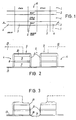
- a FAMOS transistor Flash EPROM memory device includes horizontal parallel sectors 1 having the thick oxide layer or so-called Field Oxide grown thereupon and arranged in such a way as to separate from one another the horizontal sectors 2 upon which the FAMOS transistor cells are manufactured.
- Said FAMOS transistor cells are centrally provided with a gate stack 3 which is laid upon the substrate channel separating the drain region 4 and the source region 5.
- Vertical sectors 6 constitute the source lines. Each source line is so designed as to inter-connect the various source regions 5 belonging to it in order to form the common source line for a word of the memory device. Aiming at forming this connection, as previously described, the local oxide is to be removed from each of said vertical sectors 6, by performing said SAS etch step, and the necessary dopant agent is to be implanted therein.
- a cross-section view along line A-A' of figure 1 is shown in Figure 2, in respect of a horizontal sector 2 of a device manufactured according to a conventional process, before the SAS etch step.
- a layer 7 of poly-1, a layer 8 of ONO, a layer 9 of poly-2 and a layer 10 of silicide can be observed within the gate stack 3.
- the annealing step carried out after the stack etch step causes a thin layer 11 of silicon dioxide to grow around the gate stack 3.
- a protection layer 12 of "resist” is shown in dashed line in the Figure, said protection layer being patterned according to photolithographic techniques, the resolution limits of which do not allow a perfect alignment to the edge of the gate stack 3 to be achieved. It is also possible to observe the Tunnel Oxide layer 13.
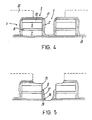
- FIG 3 A cross-section view of Figure 2 is shown in Figure 3, after having performed the SAS etch step according to a conventional manufacturing process. It can be observed that the removal of the Tunnel Oxide layer 13 (as well as of the Field Oxide layer) exposes the silicon substrate portion 14 corresponding to the source region (and line). Also, due to not-ideal anisotropy of the SAS etch operation, the oxide layer 11 existing on the side walls of the gate stack, on the side of the source region 5, appears to have been at least partially etched and particularly it appears to have been completely removed at the top section 15 and to have been noticeably thinned at the bottom section 16 of the walls, with respect to the side of the drain region 4.
- the approach suggested according to this invention provides for depositing a thin layer 17 of silicon nitride (Si 3 N 4 ) on the whole device being manufactured, said deposition being carried out after said annealing step subsequent to the stack etch step and before the photolithographic step by which the source lines are defined.
- the surface of such layer 17 of silicon nitride can be oxidized in an aqueous vapor in order to form silicon oxi-nitride.
- Such oxidation operation improves the characteristics of the concerned nitride in view of the subsequent chemical etching treatment and of the magnetic permeability.
- the SAS etching step aimed at etching the source line oxide is preceded by a plasma-assisted anisotropic chemical etching operation, of very short duration, intended to remove the nitox layer from the horizontal surfaces, so as to expose the source lines to the subsequent SAS etch step.
- a plasma-assisted anisotropic chemical etching operation of very short duration, intended to remove the nitox layer from the horizontal surfaces, so as to expose the source lines to the subsequent SAS etch step.
- Such a chemical etching operation applied to the nitox layer also designated as "break-through” operation has a very short duration and sufficient anisotropic properties as not to substantially etch the nitox layer on the vertical walls.
- said SAS etching operation is designed so as to be extremely selective in respect of the nitox layer 17 and to rapidly etch the silicon oxide.
- the oxide etching rate therefore, is extremely higher than the nitox etching rate.
- Figure 5 shows the results obtained by means of a SAS etching operation carried out by low performance equipment and, therefore, it illustrates a particularly negative case.
- higher performance apparatuses it is possible to obtain a protection of the concerned oxide layer 11 on the whole side wall of the gate stack 3 and on the top section 15, as well.
- the above illustrated nitox layer 17 is adapted to protect the oxide layer 11 on the side wall of the gate stack 3 even when the stack etch operation creates a not-sharp and tilted profile of said gate stack 3, thereby reducing the sensitivity of the manufacturing process of these devices to the possible variations of the stack etch step performances, namely enhancing the tolerance figure of the process in respect of such variations and increasing in this way the sturdiness of the process.
- the above said nitox layer 17 obviously also protects the base portion 16 of the gate stack 3 and thus prevents the Tunnel Oxide layer 13 from being etched away from below the stack itself. By maintaining such portion of said Tunnel Oxide layer 13 in integral condition, an increase in immunity to electric noise caused by write or delete operations in adjacent cells is achieved.
- the impact on the characteristics of the FAMOS transistor cells is also easily controllable.
- the increase in the length of the transistor channel, as caused by the thickness of said nitox layer 17, can be easily balanced for instance by extending the diffusion times of the implanted dopant agents or by reducing the thickness of the oxide grown during the annealing operation carried out subsequently to the stack etch step.
- the temperatures at which the deposition of nitride and its oxidation in aqueous vapour are carried out are significantly lower than the temperatures at which the thermal oxidation and dopant diffusion operations are performed. In view of this, said temperatures have a substantially negligible impact on the device being manufactured, because the sole doped regions existing before the SAS etch step are geometrically extended and have a low dopant concentration, as well.
Abstract
- a preliminary deposition of a layer of silicon nitride on the silicon oxide;
- a first anisotropic chemical etching or break-through stage, along said etching direction, aimed at removing the nitride layer from the silicon oxide surfaces ortogonal to said etching direction;
- a second anisotropic chemical etching stage along said etching direction, aimed at removing the silicon oxide surfaces orthogonal to said etching direction.
Description
- a preliminary deposition of a layer of silicon nitride (Si3N4) on the silicon oxide (SiO2);
- a first anisotropic chemical etching or break-through stage, along said etching direction, aimed at removing the nitride layer from the silicon oxide surfaces orthogonal to said etching direction;
- a second anistropic chemical etching stage along said etching direction, aimed at removing the silicon oxide surfaces orthogonal to said etching direction.
- a first set of chemical-physical treatment steps for forming the gate stacks of said FAMOS transistors, ending with an anisotropic chemical etching step, possibly plasma assisted, or stack etch step, aimed at defining the dimensions of said gate stacks and with an annealing step, under oxygen atmosphere, aimed at growing a thin layer of silicon oxide on the whole exposed surfaces of said gate stacks, and
- a second set of chemical-physical treatment steps for doping the silicon substrate in corresponding locations to the source and drain regions of said FAMOS transistors, beginning with dopant implantation in the source lines, in which the following steps are carried out between said first and second sets of chemical-physical treatment steps:
- a preliminary deposition operation of a silicon nitride layer upon said thin silicon oxide layer,
- a photolithographic process aimed at defining the areas that form the source lines,
- a first anisotropic chemical etching operation, possibly plasma assisted, or break-through step, having such an etching direction as to remove the nitride layer from said source line forming areas,
- a second anisotropic chemical etching operatiion according to said etching direction, aimed at removing said silicon oxide layer from said source line forming areas.
Claims (6)
- Improvement in the anisotropic chemical etching process of silicon oxide, having an etching direction, comprising following steps:providing a preliminary deposition of a layer (17) of silicon nitride (Si3N4) on the silicon oxide (SiO2);providing a first anisotropic chemical etching or break-through stage, along an etching direction, aimed at removing the nitride layer (17) from the silicon oxide surfaces orthogonal to said etching direction;performing a second anisotropic chemical etching stage along said etching direction, aimed at removing the silicon oxide surfaces orthogonal to said etching direction.
- Process according to claim 1, wherein, after said preliminary deposition step of a silicon nitride layer (17) a surface oxidation step of said silicon nitride layer is carried out in aqueous vapour.
- Process according to daim 1 or 2, wherein said preliminary deposition operation is a plasma-assisted chemical vapor deposition (PCVD) or a low-pressure chemical vapour deposition (LPCVP) or an energy-enhanced chemical vapour deposition.
- Process according to any one of the preceding claims, wherein said preliminary deposition operation takes place at a temperature lower than the temperatures at which the thermal oxidation of the silicon and the diffusion of the dopants are performed.
- Process according to any one of daims 2 to 4, wherein said surface oxidation in aqueous vapour of said silicon nitride layer is carried out at a temperature lower than the temperatures at which the thermal oxidisation of the silicon and the diffusion of the dopants are performed.
- A process for manufacturing fast access electrically programmable non-volatile silicon memory devices or "Flash EPROM" memory devices, based upon floating-gate avalanche-injection MOS or "FAMOS" transistors, comprising the steps of:performing a first set of chemical-physical treatment steps for forming the gate stacks (3) of FAMOS transistors, ending with an anistropic chemical etching step or stack etch step, aimed at defining the dimensions of said gate stacks (3) and with an annealing step, under oxygen atmosphere, aimed at growing a thin layer (11) of silicon oxide on the whole exposed surfaces of said gate stacks (3),performing a preliminary deposition operation of a silicon nitride layer (17) upon said thin silicon layer (11),performing a photolithographic process aimed at defining the areas (6) that form the source lines,performing a first anisotropic chemical etching operation or break-through step, having such an etching direction as to remove the nitride layer (17) from said source line forming areas (6),performing a second anisotropic chemical etching operation according to said etching direction, aimed at removing said silicon oxide layer (11) from said source line forming areas (6) and,performing a second set of chemical-physical treatment steps for doping the silicon substrate in corresponding locations to the source and drain regions of said FAMOS transistors, beginning with dopant implantation in the source lines.
Applications Claiming Priority (2)
| Application Number | Priority Date | Filing Date | Title |
|---|---|---|---|
| ITRM970430 | 1997-07-14 | ||
| IT97RM000430A IT1293535B1 (en) | 1997-07-14 | 1997-07-14 | IMPROVEMENT IN THE PROCESS OF ANISOTROPIC CHEMICAL ATTACK OF SILICON OXIDE, IN PARTICULAR IN THE MANUFACTURE OF |
Publications (2)
| Publication Number | Publication Date |
|---|---|
| EP0893820A2 true EP0893820A2 (en) | 1999-01-27 |
| EP0893820A3 EP0893820A3 (en) | 2003-10-29 |
Family
ID=11405175
Family Applications (1)
| Application Number | Title | Priority Date | Filing Date |
|---|---|---|---|
| EP98305602A Withdrawn EP0893820A3 (en) | 1997-07-14 | 1998-07-14 | Anisotropic chemical etching process of silicon oxide in the manufacture of MOS transistor flash EPROM devices |
Country Status (6)
| Country | Link |
|---|---|
| US (1) | US6110781A (en) |
| EP (1) | EP0893820A3 (en) |
| KR (1) | KR19990013849A (en) |
| IT (1) | IT1293535B1 (en) |
| SG (1) | SG71131A1 (en) |
| TW (1) | TW480620B (en) |
Cited By (1)
| Publication number | Priority date | Publication date | Assignee | Title |
|---|---|---|---|---|
| WO2006118789A2 (en) * | 2005-05-02 | 2006-11-09 | Advanced Micro Devices, Inc. | Integrated circuit and method of manufacture |
Families Citing this family (4)
| Publication number | Priority date | Publication date | Assignee | Title |
|---|---|---|---|---|
| KR100607322B1 (en) * | 1999-06-30 | 2006-07-28 | 주식회사 하이닉스반도체 | Method of manufacturing a flash EEPROM cell |
| JP4149644B2 (en) * | 2000-08-11 | 2008-09-10 | 株式会社東芝 | Nonvolatile semiconductor memory device |
| KR101024252B1 (en) * | 2003-10-30 | 2011-03-29 | 주식회사 하이닉스반도체 | Method for fabrication of semiconductor device |
| CN105070718B (en) * | 2015-08-18 | 2019-01-04 | 上海华虹宏力半导体制造有限公司 | A method of reducing SONOS memory series resistance |
Citations (7)
| Publication number | Priority date | Publication date | Assignee | Title |
|---|---|---|---|---|
| US5019879A (en) * | 1990-03-15 | 1991-05-28 | Chiu Te Long | Electrically-flash-erasable and electrically-programmable memory storage devices with self aligned tunnel dielectric area |
| US5270234A (en) * | 1992-10-30 | 1993-12-14 | International Business Machines Corporation | Deep submicron transistor fabrication method |
| US5275972A (en) * | 1990-02-19 | 1994-01-04 | Matsushita Electric Industrial Co., Ltd. | Method for fabricating a semiconductor integrated circuit device including the self-aligned formation of a contact window |
| US5397724A (en) * | 1992-06-09 | 1995-03-14 | Sony Corporation | Method of making a nonvolatile memory device having a sidewall insulating film doped with phosphorus |
| US5467308A (en) * | 1994-04-05 | 1995-11-14 | Motorola Inc. | Cross-point eeprom memory array |
| US5510282A (en) * | 1993-01-07 | 1996-04-23 | Nec Corporation | Method for manufacturing a nonvolatile semiconductor memory device using a residual sidewall film |
| US5573965A (en) * | 1991-03-27 | 1996-11-12 | Lucent Technologies Inc. | Method of fabricating semiconductor devices and integrated circuits using sidewall spacer technology |
Family Cites Families (2)
| Publication number | Priority date | Publication date | Assignee | Title |
|---|---|---|---|---|
| JP2891205B2 (en) * | 1996-10-21 | 1999-05-17 | 日本電気株式会社 | Manufacturing method of semiconductor integrated circuit |
| US5766992A (en) * | 1997-04-11 | 1998-06-16 | Taiwan Semiconductor Manufacturing Company Ltd. | Process for integrating a MOSFET device, using silicon nitride spacers and a self-aligned contact structure, with a capacitor structure |
-
1997
- 1997-07-14 IT IT97RM000430A patent/IT1293535B1/en active IP Right Grant
-
1998
- 1998-07-13 SG SG1998001761A patent/SG71131A1/en unknown
- 1998-07-14 KR KR1019980028387A patent/KR19990013849A/en not_active Application Discontinuation
- 1998-07-14 EP EP98305602A patent/EP0893820A3/en not_active Withdrawn
- 1998-07-14 US US09/115,305 patent/US6110781A/en not_active Expired - Lifetime
- 1998-08-14 TW TW087113375A patent/TW480620B/en not_active IP Right Cessation
Patent Citations (7)
| Publication number | Priority date | Publication date | Assignee | Title |
|---|---|---|---|---|
| US5275972A (en) * | 1990-02-19 | 1994-01-04 | Matsushita Electric Industrial Co., Ltd. | Method for fabricating a semiconductor integrated circuit device including the self-aligned formation of a contact window |
| US5019879A (en) * | 1990-03-15 | 1991-05-28 | Chiu Te Long | Electrically-flash-erasable and electrically-programmable memory storage devices with self aligned tunnel dielectric area |
| US5573965A (en) * | 1991-03-27 | 1996-11-12 | Lucent Technologies Inc. | Method of fabricating semiconductor devices and integrated circuits using sidewall spacer technology |
| US5397724A (en) * | 1992-06-09 | 1995-03-14 | Sony Corporation | Method of making a nonvolatile memory device having a sidewall insulating film doped with phosphorus |
| US5270234A (en) * | 1992-10-30 | 1993-12-14 | International Business Machines Corporation | Deep submicron transistor fabrication method |
| US5510282A (en) * | 1993-01-07 | 1996-04-23 | Nec Corporation | Method for manufacturing a nonvolatile semiconductor memory device using a residual sidewall film |
| US5467308A (en) * | 1994-04-05 | 1995-11-14 | Motorola Inc. | Cross-point eeprom memory array |
Cited By (4)
| Publication number | Priority date | Publication date | Assignee | Title |
|---|---|---|---|---|
| WO2006118789A2 (en) * | 2005-05-02 | 2006-11-09 | Advanced Micro Devices, Inc. | Integrated circuit and method of manufacture |
| WO2006118789A3 (en) * | 2005-05-02 | 2007-11-08 | Advanced Micro Devices Inc | Integrated circuit and method of manufacture |
| GB2439883A (en) * | 2005-05-02 | 2008-01-09 | Advanced Micro Devices Inc | Integrated circuit and method of manufacture |
| GB2439883B (en) * | 2005-05-02 | 2010-08-11 | Advanced Micro Devices Inc | Integrated circuit and method of manufacture |
Also Published As
| Publication number | Publication date |
|---|---|
| EP0893820A3 (en) | 2003-10-29 |
| US6110781A (en) | 2000-08-29 |
| SG71131A1 (en) | 2000-03-21 |
| IT1293535B1 (en) | 1999-03-01 |
| KR19990013849A (en) | 1999-02-25 |
| ITRM970430A0 (en) | 1997-07-14 |
| TW480620B (en) | 2002-03-21 |
| ITRM970430A1 (en) | 1999-01-14 |
Similar Documents
| Publication | Publication Date | Title |
|---|---|---|
| US8063429B2 (en) | Conductive spacers extended floating gates | |
| US5599727A (en) | Method for producing a floating gate memory device including implanting ions through an oxidized portion of the silicon film from which the floating gate is formed | |
| KR100373285B1 (en) | Nonvolatile semiconductor memory device and manufacturing method thereof | |
| US5474947A (en) | Nonvolatile memory process | |
| US5972751A (en) | Methods and arrangements for introducing nitrogen into a tunnel oxide in a non-volatile semiconductor memory device | |
| KR100697353B1 (en) | Method for providing a dopant level for polysilicon for flash memory devices | |
| US7238575B2 (en) | Fabrication of conductive lines interconnecting conductive gates in nonvolatile memories, and non-volatile memory structures | |
| US6746920B1 (en) | Fabrication method of flash memory device with L-shaped floating gate | |
| JPH02292870A (en) | Structureof flash type high density eeprom semiconductor memory and its manufacture including manufac- -turing process | |
| US6784039B2 (en) | Method to form self-aligned split gate flash with L-shaped wordline spacers | |
| US6248635B1 (en) | Process for fabricating a bit-line in a monos device using a dual layer hard mask | |
| US7443725B2 (en) | Floating gate isolation and method of making the same | |
| US7414282B2 (en) | Method of manufacturing a non-volatile memory device | |
| JP2006509366A (en) | Self-aligned shallow trench isolation with improved coupling coefficient in floating gate devices | |
| US7172938B2 (en) | Method of manufacturing a semiconductor memory device | |
| US6110781A (en) | Anisotropic chemical etching process of silicon oxide in the manufacture of MOS transistor flash EPROM devices | |
| US8318566B2 (en) | Method to seperate storage regions in the mirror bit device | |
| US6236081B1 (en) | AND-type non-volatile semiconductor memory device and method of manufacturing thereof | |
| US6034395A (en) | Semiconductor device having a reduced height floating gate | |
| US6207502B1 (en) | Method of using source/drain nitride for periphery field oxide and bit-line oxide | |
| US20050054161A1 (en) | Method of decreasing charging effects in oxide-nitride-oxide (ONO) memory arrays | |
| US7977227B2 (en) | Method of manufacturing a non-volatile memory device | |
| JP2000058682A (en) | Improvement of anisotropical chemical etching method of silicon oxide in manufacturing mos transistor flash eprom device | |
| KR20050068901A (en) | Method for fabricating a non-volatile memory device | |
| KR100545209B1 (en) | A method for manufacturing a cell of flash memory cell |
Legal Events
| Date | Code | Title | Description |
|---|---|---|---|
| PUAI | Public reference made under article 153(3) epc to a published international application that has entered the european phase |
Free format text: ORIGINAL CODE: 0009012 |
|
| AK | Designated contracting states |
Kind code of ref document: A2 Designated state(s): AT BE CH CY DE DK ES FI FR GB GR IE IT LI LU MC NL PT SE |
|
| AX | Request for extension of the european patent |
Free format text: AL;LT;LV;MK;RO;SI |
|
| RIN1 | Information on inventor provided before grant (corrected) |
Inventor name: CAUTIERO, GIUSEPPE Inventor name: CHINTAPALLI, KOTESWARA RAO Inventor name: TORSI, ALESSANDRO Inventor name: MICCOLI, GIUSEPPE Inventor name: RUSSO, FELICE |
|
| PUAL | Search report despatched |
Free format text: ORIGINAL CODE: 0009013 |
|
| RIC1 | Information provided on ipc code assigned before grant |
Ipc: 7H 01L 21/336 B Ipc: 7H 01L 27/115 B Ipc: 7H 01L 21/8247 B Ipc: 7H 01L 21/314 B Ipc: 7H 01L 21/311 A |
|
| AK | Designated contracting states |
Kind code of ref document: A3 Designated state(s): AT BE CH CY DE DK ES FI FR GB GR IE IT LI LU MC NL PT SE |
|
| AX | Request for extension of the european patent |
Extension state: AL LT LV MK RO SI |
|
| 17P | Request for examination filed |
Effective date: 20040429 |
|
| RAP1 | Party data changed (applicant data changed or rights of an application transferred) |
Owner name: CONSORZIO EAGLE Owner name: TEXAS INSTRUMENTS INCORPORATED |
|
| AKX | Designation fees paid |
Designated state(s): DE FR GB IT NL |
|
| 17Q | First examination report despatched |
Effective date: 20040713 |
|
| STAA | Information on the status of an ep patent application or granted ep patent |
Free format text: STATUS: THE APPLICATION IS DEEMED TO BE WITHDRAWN |
|
| 18D | Application deemed to be withdrawn |
Effective date: 20041124 |
|
| RAP1 | Party data changed (applicant data changed or rights of an application transferred) |
Owner name: CONSORZIO EAGLE Owner name: TEXAS INSTRUMENTS INCORPORATED |