EP0897154A2 - Memory controller supporting dram circuits with different operating speeds - Google Patents
Memory controller supporting dram circuits with different operating speeds Download PDFInfo
- Publication number
- EP0897154A2 EP0897154A2 EP98306426A EP98306426A EP0897154A2 EP 0897154 A2 EP0897154 A2 EP 0897154A2 EP 98306426 A EP98306426 A EP 98306426A EP 98306426 A EP98306426 A EP 98306426A EP 0897154 A2 EP0897154 A2 EP 0897154A2
- Authority
- EP
- European Patent Office
- Prior art keywords
- memory
- data
- processor
- computer system
- clock
- Prior art date
- Legal status (The legal status is an assumption and is not a legal conclusion. Google has not performed a legal analysis and makes no representation as to the accuracy of the status listed.)
- Withdrawn
Links
Images


Classifications
-
- G—PHYSICS
- G06—COMPUTING; CALCULATING OR COUNTING
- G06F—ELECTRIC DIGITAL DATA PROCESSING
- G06F13/00—Interconnection of, or transfer of information or other signals between, memories, input/output devices or central processing units
- G06F13/14—Handling requests for interconnection or transfer
- G06F13/16—Handling requests for interconnection or transfer for access to memory bus
- G06F13/1668—Details of memory controller
- G06F13/1694—Configuration of memory controller to different memory types
Definitions
- the present invention relates generally to a computer system including a system memory comprised of a dynamic random access memory (DRAM) array. More particularly, the invention relates to a memory controller for controlling data transfers between computer components and dynamic random access memory. Still more particularly, the invention relates to a memory controller capable of supporting different speed DRAM devices within a memory array.
- DRAM dynamic random access memory
- a computer system that includes a specially configured memory controller for controlling memory cycles to a plurality of banks of synchronous dynamic random access memory (SDRAM) devices.
- SDRAM synchronous dynamic random access memory
- the SDRAM memory devices may operate at different frequencies appropriate for each SDRAM device and need not operate at the same frequency as the processor.
- a memory controller generates multiple clock signals with different frequencies for use by the different SDRAM memory devices.
- the input queue logic 304 determines which buffer in the queue write buffer 320 will receive the write data on bus 321.
- the input queue logic 304 provides an input queue pointer 307 to queue write buffer 320 that identifies which of the four buffers processor control 202 is to receive the data to be written. Thus, as buffer 0 becomes full, input queue pointer 307 increments to point to buffer 1, which then fills with data from processor control 202.
- Input queue logic 304 includes logic to determine when input queue pointer 307 must be incremented.
- processor control 202 asserts the asynch ready signal on line 305 which is provided as an input to input queue logic 304, as well as to signal synchronizer 302. One asynch ready signal is provided for each buffer 0-3.
- the asynch ready signal associated with a buffer is relayed to memory control 206 to indicate that the associated buffer contains data to be read by memory control 202.
- input queue logic 304 increments input queue pointer 307.
- output queue logic 308 includes a register 319 and an output queue pointer 309.
- Register 319 includes a valid bit for each buffer in queue write buffer 320.
- Each buffer valid bit in register 319 identifies whether data is present in the associated buffer that has not been read by memory control 206.
- the asynch ready signal on line 305 is asserted by processor control 202.
- the asynch ready signal is also asserted on line 306 by signal synchronizer 302 and provided to memory control 206 and output queue logic 308.
- Output queue logic 308 uses the asynch ready signal to set the valid bit associated with the asynch ready signal to indicate that the buffer includes data to be read by memory control 206.
- the present invention enables a processor to read data from and write data to one or more SDRAM banks in system memory, and also enables each SDRAM bank to operate at a clock frequency different from that of the processor clock.
- P2MQ 300 receives a processor clock signal on line 311 and a memory clock signal on line 312.
- Input queue logic 304 transfers data into the queue write buffer 320 using the processor clock signal.
- the signal synchronizer 302 and input queue logic 304 connect to line 311 to receive the processor clock signal.
- the signal synchronizer 302 and output queue logic 308 connect to line 312 to receive the memory clock signal.
- the interface between the system processor and the processor to memory queue 300 occurs in the processor clock domain.
- the interface between the memory array and the processor to memory queue 300 occurs in the memory clock domain.
- the SPD standard requires the following information to be implemented in all memory devices designed to the SPD standard.
- clock switch control signals on lines 526, 527 are generated by clock switch logic 525 which produces the appropriate control signals as defined by bank control speed register 520.
- clock switch logic 525 By reading the two speed control bits associated with each bank, clock switch logic 525 generates the appropriate switch control bits to direct each multiplexer 506 is provide a clock frequency corresponding to the speed control bits.
- the clock switch logic preferably is capable of selecting different frequencies for each multiplexer at any time.
Abstract
Description
- The present invention relates generally to a computer system including a system memory comprised of a dynamic random access memory (DRAM) array. More particularly, the invention relates to a memory controller for controlling data transfers between computer components and dynamic random access memory. Still more particularly, the invention relates to a memory controller capable of supporting different speed DRAM devices within a memory array.
- Personal computers typically include dynamic random access memory ("DRAM") chips, commonly referred to as system memory. DRAM memory operates asynchronously, meaning read and write requests do not necessarily coincide with a clock signal. Further, DRAM memory must be refreshed periodically to maintain the data stored in the chip. Normally, system memory includes banks ofDRAM devices. Each memory bank may include as many as eight or nine memory chips. The number of banks provided in a computer system varies, but a typical range is between one and eight banks.
- According to normal convention, the DRAM banks comprise the working memory of the system processor. The DRAM array connects to the memory controller via a memory bus, comprised of memory address lines, memory data lines, and various control lines. Data generally is transferred between the DRAM array and other components in two steps. Fist, the accessing component generates signals on the address lines representing the row address of the desired memory location, which are latched into the DRAM when the row address strobe (RAS) signal is asserted. At the next, or at subsequent, clock cycles, the DRAM latches in the column address signals when the column address strobe (CAS) signal is asserted. After the memory address has been determined, the memory array latches in data or drives out data, depending upon the status of the read/write (R/W) control signal.
- The speed of memory devices is based upon certain timing parameters. These parameters require a certain period oftime to perform a memory operation. Because ofthese timing parameters, memory constructed with DRAM circuits is not always capable of responding to memory accesses within the time period allotted by the processor. In this event, external circuitry must signal to the processor that supplementary processor cycles, or wait states, are necessary before the data is ready on the data bus, or before data on the data bus can be stored in memory. In addition to slowing the system processor, wait states typically require use of the CPU host bus, thereby limiting use of that bus by other system components.
- Recently, memory device manufacturers have introduced synchronous DRAM ("SDRAM") to alleviate the memory bottleneck that occurs using conventional DRAM devices. Synchronous DRAM devices require a clock signal as a control input signal. SDRAM devices, like DRAM chips, are commonly organized into memory banks in an array. Many computer systems available today permit as many as eight banks in the memory array. The SDRAM device derives its name from the fact that all ofthe input signals (or commands) are accepted by the DRAM device on the rising edge of the clock signal, and thus are "synchronized" with the clock signal. The clock signal also allows data pipelining within the memory array and permits data to be output in a continuous stream.
- SDRAM devices currently are available in different speeds (which typically is measured in units of frequency, such as megahertz, which indicate the number of cycles per second for the device). Today, SDRAM devices are available as 66 MHz or 100 MHz devices, although higher speeds are expected. The price of SDRAM devices generally is dependent on frequency, with higher speed devices costing more.
- The transfer and timing of address, data and control signals between a processor and a DRAM device is controlled by a memory controller. Memory controllers control transactions between the system memory and other components in the computer system, including the central processing unit. In some computer systems, the memory controller couples to a peripheral component interconnect ("PCr') bus to permit masters on the PCI bus to run cycles to the system memory. In accordance with normal convention, memory control units provide a clock signal to each bank in the SDRAM memory array. Often, because of loading problems and other concerns, memory controllers provide two separate output clock signals to clock up to eight memory banks, which each clock signal connected to up to four memory banks.
- As faster microprocessors become available and are implemented in computer designs, memory devices must operate faster to minimize processor wait states and to maintain compatibility with the processors. Because ofthe cost of memory devices, consumers prefer to salvage memory devices from old computers and re-use these memory devices in new computer systems. However, the use of faster processors in the new computer systems typically precludes the use of older, slower memory. Thus, as computer manufacturers offer faster computer systems, computer owners are unable to re-use memory devices from older computers. In large computer systems, such as file servers, the expenditure on system memory represents a substantial investment.
- It would be advantageous to develop a computer system that is capable ofusing older memory devices when upgrading to a new computer system. At least one option has been suggested to accomplish this goal. That option is to run the computer system at the speed of the slowest memory device. Although faster memory devices will operate at the slower speed, the overall computer performance is compromised because data communications with the memory array are performed at a speed less than that at which the faster memory devices can operate.
- It would thus be desirable to provide a computer system that is capable of implementing memory devices with different operating speeds. It would also be desirable ifthe computer system could optimize the performance of each memory device by performing transactions at the fastest possible speed with each memory circuit. By performing transactions at the maximum speed of each memory device, overall computer performance would be increased.
- Despite the apparent advantage of a computer system capable of operating with SDRAM devices of different speeds, to date no such system has been built.
- The problems outlined above are in large part solved by a computer system that includes a specially configured memory controller for controlling memory cycles to a plurality of banks of synchronous dynamic random access memory (SDRAM) devices. The SDRAM memory devices may operate at different frequencies appropriate for each SDRAM device and need not operate at the same frequency as the processor. In accordance with the preferred embodiment, a memory controller generates multiple clock signals with different frequencies for use by the different SDRAM memory devices.
- The memory controller preferably includes asynchronous data queues to facilitate data transfers between the SDRAM memory array and either the processor or a master on the PCI bus or other system bus. Upon initialization, the computer system determines the type of SDRAM devices present in the memory array and provides that information to the memory controller which, in response, generates clock signals to the various SDRAM devices in the memory array. The frequencies of the clock signals provided by the memory controller are appropriate for the SDRAM devices in the computer system. According to a preferred embodiment, information stored in each SDRAM device identifies the type of memory circuit and is used to determine the type of SDRAM devices included in the computer system.
- A better understanding of the present invention can be obtained when the following detailed description of the preferred embodiment is considered in conjunction with the following drawings, in which:
- Figure 1 is a block diagram of a computer system including a memory and PCI bridge controller, processor to memory, memory to processor data queues and memory clock generator consistent with the preferred embodiment;
- Figure 2 is a block diagram ofthe memory and PCI bridge controller in accordance with the preferred embodiment of Figure 1;
- Figure 3 is a block diagram illustrating in more detail the processor to memory data queue of Figure 1;
- Figure 4a shows a dual flip flop circuit for converting a signal between two clock domains;
- Figure 4b is a timing diagram of the dual flip flop circuit of Figure 4a;
- Figure 5 is a block diagram illustrating in more detail the memory to processor data queue of Figure 1; and
- Figure 6 is a block diagram of the memory clock generator of Fig. 1.
-
- Referring now to Figure 1, the
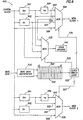
computer system 100 constructed in accordance with the preferred embodiment generally includes aprocessor 102 coupled to a memory andPCI bridge controller 200 through aCPU host bus 104. The memory andPCI bridge controller 200 includes a memory controller for orchestrating data transfers with thesystem memory array 114 viamemory bus 112. The memory andPCI bridge controller 200 also function as a bus bridge to the peripheral component interconnect (PCI)bus 106. In accordance with normal convention, various devices can be coupled to thePCI bus 106, such as agraphics card 108, a local area network ("LAN")interface 110, or any other PCI bus device. Such PCI devices preferably operate in a mastership mode, according to known techniques, to write data to and read data from thememory array 114. -
Processor 102 may include any microprocessor such as a Pentium® processor with MMX™ technology, Pentium II processor, K-6, or any other processor capable of being used in a personal computer. Moreover, while only one processor is shown, one skilled in the art will understand that multiple processors may be provided in the computer system. Similarly, theCPU host bus 104 andPCI bus 106 include bus architectures commonly used in personal computers. - The
memory array 114 preferably comprises synchronous dynamic random access memory ("SDRAM") devices such as the PD4516421 SDRAM manufactured by NEC Electronics, or any other SDRAM device. Thememory array 114 may be organized in banks in accordance with normal convention. Each bank of SDRAM memory may have SDRAM devices with the same or different timing and speed characteristics. Further, the clock frequency of the SDRAM devices may be different than the frequency of the processor clock. The memory andPCI bridge controller 200 enables thecomputer system 100 to write data to and read data from thesystem memory array 114 even though the memory array may include a mix of different speed SDRAM devices. The implementation of a memory andPCI bridge controller 200 that can communicate with different speed SDRAM's makes it unnecessary to modify or specially design theprocessor 102 and the devices coupled toPCI bus 106 to communicate with multiple speed SDRAM devices. - Referring now to Figures 1 and 2, the memory and
PCI bridge controller 200 preferably includes a processorcontrol interface unit 202, a PCIbus control interface 204, and amemory control unit 206. Theprocessor control 202 provides logic for interfacing thecontroller 200 tosystem processor 102. Similarly, thePCI control 204 provides logic for interfacing the controller toPCI bus 106 andmemory control 206 includes logic for interfacingcontroller 200 to thememory bus 112. Data and address signals are transferred between theprocessor control 202 andmemory control 206 via processor-to-memory data queue (P2MQ) 300 and memory-to-processor data queue (M2PQ) 350. Data written to the memory array is temporarily stored inP2MQ 300 while data read from the memory array is temporarily stored inM2PQ 350. Similarly, data written to memory byPCI bus control 204 is buffered in PCI-to-memory queue (PCI2MQ) 400 and data read from memory byPCI control 204 is buffered in memory to PCI (M2PCIQ)queue 450. - Memory and
PCI bridge controller 200 also includes amemory clock generator 500 for generating multiple memory clock signals. Three such clock signals are shown for purposes of illustration in Figure 2 asmemory clock 1,memory clock 2 andmemory clock 3 Althoughmemory clock generator 500 is shown as part of memory andPCI bridge controller 200, thememory clock generator 500 may alternatively be constructed as a separate component. As explained below, the memory clock signals are derived from the system clock (also referred to as the processor bus clock). The memory clock signals may include different frequencies and thus allow different speed SDRAM's to be used incomputer system 100.Memory clock generator 500 is programmed to provide an appropriate clock frequency based on BIOS data provided as an input to thememory clock generator 500. The BIOS data identifies the type of SDRAMs included in each bank. - Because the SDRAM devices may operate at speeds that differ from
processor 102,data queues P2MQ 300,M2PQ 350,PCI2MQ 400 andM2PCIQ 450 function to synchronize the data flow between the memory array and theprocessor 102 and between thememory array 114 and PCI bus masters. Accordingly,computer system 100 preferably includes a set ofdata queues PCI bridge 200 in Figure 2 is shown to include only data queues for one bank of SDRAM devices, the memory andPCI bridge 200 may include additional sets ofdata queues memory array 114. The operation of the data queues, as well as thememory clock generator 500 is explained in more detail below. - Referring now to Figures 2 and 3, during a write cycle to memory from the system processor, data and address signals pass through the processor to
memory queue P2MQ 300. As shown in Figure 3,P2MQ 300 preferably includesinput queue logic 304,output queue logic 308, queue writebuffer 320, andsignal synchronizer 302. In addition to data and address signals, the processor also preferably transmits certain control signals to the processor tomemory queue P2MQ 300, including a processor clock signal and an asynch ready signal. The processor also receives two control signals from theP2MQ 200, including a cycle done signal and a buffer full signal. Similarly, the memory control provides a memory clock signal and a cycle done signal to theP2MQ 200. TheP2MQ 200 provides an asynch ready control signal to the primary controller. - The
processor control 202 transfers data, address and cycle information to theP2MQ 300 andbus 321. The cycle information generally includes such information as byte enables, write back bits, and burst bits and are used for reads and writes in accordance with known techniques. The queue writebuffer 320 couples tobus 321, and preferably includes four buffers,buffer 0,buffer 1,buffer 2, andbuffer 3. Each buffer in thequeue write buffer 320 preferably is one cache line in width and thus may hold 32 bytes of data along with address and cycle information. It should be recognized, however, that queue writebuffer 320 can include any number of buffers and each buffer may be any number of bits in width. - The
input queue logic 304 determines which buffer in thequeue write buffer 320 will receive the write data onbus 321. Theinput queue logic 304 provides aninput queue pointer 307 to queuewrite buffer 320 that identifies which of the fourbuffers processor control 202 is to receive the data to be written. Thus, asbuffer 0 becomes full,input queue pointer 307 increments to point tobuffer 1, which then fills with data fromprocessor control 202.Input queue logic 304 includes logic to determine wheninput queue pointer 307 must be incremented. When a buffer becomes full,processor control 202 asserts the asynch ready signal online 305 which is provided as an input to inputqueue logic 304, as well as to signalsynchronizer 302. One asynch ready signal is provided for each buffer 0-3. The asynch ready signal associated with a buffer is relayed tomemory control 206 to indicate that the associated buffer contains data to be read bymemory control 202. Upon detection of an asserted asynch ready signal,input queue logic 304 incrementsinput queue pointer 307. -
Input queue logic 304 also includes aregister 318, which includes four status bits corresponding to each ofthe buffers in thequeue write buffer 320. Each buffer status bit indicates whether the associated buffer has been read bymemory control 206. As a buffer is provided with data byprocessor control 202, the corresponding buffer status bit inregister 318 is set to indicate that data is present in the buffer, and thememory control 206 has not yet read data from that buffer. Each buffer status empty bit inregister 318 is cleared when thememory control 206 reads data from the buffer associated with the buffer bit. By updating and monitoring the state of the buffer status bits inregister 318,input queue logic 304 can determine when thequeue write buffer 320 is full so thatprocessor control 202 does not overwrite valid buffer data that has not yet been read bymemory control 206. Upon detection of a fullqueue write buffer 320,input queue logic 304 asserts the buffer full signal online 310 to notifyprocessor control 202 of the buffer full condition. In response, theprocessor control 202 will not write additional data to queuewrite buffer 320 untilmemory control 206 has read data from one of buffers 0-3, thereby freeing a write buffer for new write data.Input queue logic 304 deasserts the buffer full signal whenmemory control 206 reads data from a previously full buffer. - Referring still to Figures 2 and 3,
output queue logic 308 includes aregister 319 and anoutput queue pointer 309.Register 319 includes a valid bit for each buffer in queue writebuffer 320. Each buffer valid bit inregister 319 identifies whether data is present in the associated buffer that has not been read bymemory control 206. As data is written into a buffer byprocessor control 202, the asynch ready signal online 305 is asserted byprocessor control 202. The asynch ready signal is also asserted online 306 bysignal synchronizer 302 and provided tomemory control 206 andoutput queue logic 308.Output queue logic 308 uses the asynch ready signal to set the valid bit associated with the asynch ready signal to indicate that the buffer includes data to be read bymemory control 206. Oncememory control 206 has read the data from a buffer, the corresponding valid bit inregister 320 is cleared to preventmemory control 206 from wrapping around and re-reading a buffer that has already been read. Thus, before or when a buffer is read, the state of that buffer's valid bit is ascertained to determine whether the buffer should be read. -
Output queue pointer 309 identifies the buffer from whichmemory control 206 reads data. At reset, the input and output queue pointers points to the same buffer. Whenmemory control 206 completes reading data from one of buffers 0-3,output queue logic 308 incrementsoutput queue pointer 309.Output queue pointer 309 thus points to the next buffer to be read bymemory control 206. Oncememory control 206 has completed reading data from one of buffers 0-3, the memory control asserts the cycle done signal online 331 to thesignal synchronizer 302. In the preferred embodiments, one cycle done signal is provided for each buffer in thequeue write buffer 320. The cycle done signal also is asserted online 301 bysignal synchronizer 302 and provided toprocessor control 202 to indicate that thememory control 206 has read data from the buffer identified by the cycle done signal. - The present invention enables a processor to read data from and write data to one or more SDRAM banks in system memory, and also enables each SDRAM bank to operate at a clock frequency different from that of the processor clock.
P2MQ 300 receives a processor clock signal online 311 and a memory clock signal online 312.Input queue logic 304 transfers data into thequeue write buffer 320 using the processor clock signal. Thesignal synchronizer 302 andinput queue logic 304 connect to line 311 to receive the processor clock signal. Similarly, thesignal synchronizer 302 andoutput queue logic 308 connect to line 312 to receive the memory clock signal. The interface between the system processor and the processor tomemory queue 300 occurs in the processor clock domain. The interface between the memory array and the processor tomemory queue 300, however, occurs in the memory clock domain. - The memory clock is provided to the
output queue logic 308 and data is read from queue writebuffer 320 bymemory control 206 using the memory clock signal. Because thedata queue 300 interfaces withprocessor control 202 andmemory control 206 using their respective clock signals, theprocessor 102 can write data to SDRAM circuits that operate at frequencies that differ fromprocessor 102. - In addition to providing data buffers to allow for clock asynchronism between
processor control 202 andmemory control 206,P2MQ 300 also includessignal synchronizer 302 which functions to synchronize the two different clock domains (processor clock and memory clock). Referring still to Figures 2 and 3,signal synchronizer 302 preferably synchronizes the asynch ready signals and the cycle done signals.Synchronizer 302 insures that a signal asserted in the processor clock domain can be accurately detected bymemory control 206 operating in the memory clock domain, and that a signal asserted in the memory clock domain can be accurately detected byprocessor control 202. - Synchronism preferably is accomplished by stretching a signal so that it is asserted for additional clock pulses. Referring now to Figures 3 and 4a,
signal synchronizer 302 preferably includestiming logic 332 and twoflip flops line 331 to the processor clock, with the understanding that comparable circuitry preferably is used to synchronize other signals, such as the asynch ready signal. - The timing diagram in Figure 4b demonstrates the timing ofthe
timing logic circuit 332 of Figure 4a. Referring now to Figures 2, 4a and 4b, the cycle done signal is asserted bymemory control 206 in the memory clock domain andtiming logic 332 stretches the cycle done signal to include two memory clock rising edges as indicated by the dashedlines processor control 202. The stretched cycle done signal online 333 is clocked throughflip flops line 301 toprocessor control 202. Flip flops 334, 335 are both clocked usingprocessor clock 311. In the preferred embodiment, flipflops - Thus, after the cycle done signal is asserted by
memory control 206 and stretched by timinglogic 332,flip flop 334 is clocked by a rising edge ofthe processor clock online 311. The stretched cycle done signal then is clocked throughflip flop 335 on the next rising edge of the processor clock. The use of two sequentially clocked flip flops avoids setup and hold timing problems that might otherwise occur ifthe cycle done signal (which originally is asserted in the memory clock domain) is not asserted long enough for a flip flop (which is clocked in the processor clock domain) to latch the signal onto its output pin. Thus, if only a single flip flop is used, that flip flop might enter a metastable state. The use of dual-clocked flip flops avoids this problem. - It should be recognized that if the stretched cycle done signal has a period of two memory clock cycles, then the period ofthe processor clock must be no greater than twice the period of the memory clock signal, minus the setup and hold times of the flip flops. That is,
PCI bridge 200 allowsprocessor 102 andPCI master devices - The circuit of Figure 4a is also used to synchronize the asynch ready signal in the processor clock domain with the memory clock domain. Instead of clocking flip flops 302a, 302b with the processor clock, however, the memory clock is used. In this case, the period of the memory clock must be:
- In the event that the processor clock and the memory clock are in phase, the asynch ready and cycle done signals need not be synchronized by
synchronizer 302. In that case the asynch ready and cycle done signals bypass the synchronizer. The processor and memory clocks are in phase when their rising edges align which may occur when the frequency of the clocks are the same or when the frequency of one clock signal is an integer multiple of the frequency of the other clock signal. Similarly, when the processor and memory clocks are in phase, the buff_rdy signal (Figure 5) also may bypass the signal synchronizer. - Referring now to Figures 2 and 5, the memory to processor queue (M2PQ) 350 preferably includes
input queue logic 355,output queue logic 360, queue readbuffer 370, andsignal synchronizer 302. Queue readbuffer 370 preferably includes two data buffers,buffer 0 andbuffer 1. Data read from the memory array to the system processor is preferably stored temporarily in one of the data buffers 0, 1 in queue readbuffer 320. Data is placed indata buffers memory control 206 and read out byprocessor control 202. -
Buffers buffer 370 preferably include four segments, or queue words, 371, 372, 373, 374. Each segment preferably is 8 bytes wide and thus the buffers are 32 bytes wide. Theinput queue logic 355 receives an M2PRDY signal frommemory control 206, and provides aninput buffer pointer 356 and an inputqueue word pointer 357 to queue readbuffer 370. Theinput buffer pointer 356 identifies the buffer, while the inputqueue word pointer 357 identifies the queue word in which data is placed bymemory control 206. Whenmemory control 206 provides data to queue readbuffer 370,memory control 206 asserts the memory-to-processor ready (M2PRDY) signal to inputqueue logic 355. In response, theinput queue logic 355 identifies the buffer and the buffer location where the data is to be stored. The buffer is identified byinput buffer pointer 356. Theinput queue logic 355 increments the inputqueue word pointer 357 to identify the queue word in which the next word of data is to be driven bymemory control 206. Once data for a transaction in a buffer has been received, thememory control 206 asserts a buffer ready (buff_rdy) signal to thesignal synchronizer 302, which in turn transmits the buff_rdy signal to theprocessor control 202. The buff_rdy signal indicates toprocessor control 202 that a buffer is full and is ready to be read by theprocessor control 202. -
Output queue logic 360 similarly provides anoutput buffer pointer 361 and an outputqueue word pointer 362 to enableprocessor control 202 to read the appropriate data from queue readbuffer 370.Processor control 202 provides a pointer increment signal to output queue logic. Upon detection of an asserted buff_rdy signal,processor control 202 asserts the pointer increment signal. In response to the pointer increment signal, output queue logic incrementsoutput buffer pointer 361 to enableprocessor control 202 to read the first queue word of data from the appropriate buffer.Output queue logic 360 then increments the outputqueue word pointer 362 to enableprocessor control 202 to read subsequent queue words of data. - Data reads and writes between devices on the PCI bus and SDRAM memory 114 (Figure 2) use similar logic to that described above regarding processor to memory reads and writes. The PCI to memory queue (PCI2MQ) 400 preferably is constructed in similar fashion to the
P2MQ 400 in Figure 3 and the memory to PCI queue (M2PCIQ) 450 preferably is constructed in similar fashion to theM2PQ 350 in Figure 5. One skilled in the art will understand that thePCI bus control 204 transmits and receives appropriate PCI protocol signals for interfacing with components residing on the PCI bus. To the extent signal synchronization is required (i.e., when the PCI clock and memory clocks are out of phase, asignal synchronizer 302 is used). Programming SDRAM bank timing parameters - Referring again to Figure 1,
computer system 100 preferably allows communication with banks of SDRAM devices that require different clock frequencies, as well as other timing parameters. For memory andPCI bridge controller 200 to effectuate data writes to and reads frommemory array 114,computer system 100 must determine which types of SDRAM devices are present in the system memory. The memory type information is supplied to memory andPCI bridge controller 202, which uses the information to drive an appropriate clock signal frequency to each bank ofSDRAM 114 and to provide certain other timing parameters appropriate for each bank of memory chips. - Although various techniques for determining the type of SDRAM devices present in the system memory are possible, the
computer system 100 preferably uses the Serial Presence Detect (SPD) information stored in theSDRAM array 114. The SPD standard defines various features of a memory device and stores that information permanently in the memory device. Those locations in the memory device containing the SPD information can be accessed through normal read cycles. In accordance with the preferred embodiment,computer system 100 retrieves the SPD information from all banks ofmemory 114 during system initialization and supplies that information to memory andPCI bridge controller 200 using the BIOS feature in the computer. - The SPD standard requires the following information to be implemented in all memory devices designed to the SPD standard.
SPD Content Description Data Type Address Map SPD size Look-up table (LUT) Entry 0 Total SPD memory size LUT Entry 1 Fundamental memory type LUT Entry 2 Definition of features specific to fundamental memory 3-31 (Optional) Superset memory type 32 (Optional) Definition of features specific to the superset memory 33-61 SPD revision designator LUT 62 Checksum for bytes 0-62 Checksum 63 Manufacturer's Jedec IC code per JEP-106 LUT 64-71 Manufacturing location Supplier unique 72 Manufacturer's part number Supplier unique 73-90 Revision code Supplier unique 91-92 Manufacturing date Binary coded decimal 93-94 Assembly serial number Supplier unique 95-98 Manufacturer specific data Supplier unique 99-125 Reserved N/A 126-127 Open free-form area Application specific 128-255 - Thus,
computer system 100 can determine whether SDRAM devices are present by reading the second byte of SPD information (as shown in Table I above) corresponding to the fundamental memory type. According to the SPD standard, an SDRAM device is identified by an hexadecimal value in the second byte of SPD information. Further, by accessing other SPD information, such as the manufacturer's part number in bytes 73-90,computer system 100 can determine the specific type of SDRAM device present and thus, that circuit is preferred clock frequency and timing characteristics. - Referring now to Figures 2 and 6,
memory clock generator 500 includesBIOS data interpreter 510, bankspeed control register 520, and memorytiming control register 522. Once the SPD information for the SDRAM banks is accessed during initialization, that information preferably is provided to memory andPCI bridge controller 200, and more specifically tomemory clock generator 500 as BIOS data. As shown in figure 6, specific information for each bank of SDRAM devices preferably is provided toBIOS data interpreter 510. - The memory specific BIOS information is interpreted by
BIOS data interpreter 510, which determines the appropriate memory clock frequency for the memory device and stores the clock frequency information in bankspeed control register 520. The size of the bankspeed control register 520 depends on the number of possible banks provided incomputer system 100 and the number of different clock frequenciesmemory clock generator 500 may provide. As an example, bankspeed control register 520 may be a sixteen bit register with two bits dedicated for speed control definition for eight memory banks. With two bits of bank speed control definition, one of four different memory clock frequencies can be selected. If more than four memory clock frequencies are available incomputer system 100, bankspeed control register 520 can be expanded to include additional bits of speed control information. Table II defines the four possible clock frequencies for each bank of SDRAM devices given two bits of speed control definition in bankspeed control register 520.Bank Speed Control Register Bits 15:14 Bank 7 Speed Select 00 = memory speed 001= memory speed 110 = memory speed 211 = memory speed 3Bits 13:12 Bank 6 Speed Select 00 = memory speed 001= memory speed 110 = memory speed 211 = memory speed 3Bits 11:10 Bank 5 Speed Select 00 = memory speed 001= memory speed 110 = memory speed 211 = memory speed 3Bits 9:8 Bank 4 Speed Select00 = memory speed 001= memory speed 110 = memory speed 211 = memory speed 3Bits 7:6 Bank 3 Speed Select00 = memory speed 001= memory speed 110 = memory speed 211 = memory speed 3Bits 5:4 Bank 2 Speed Select00 = memory speed 001= memory speed 110 = memory speed 211 = memory speed 3Bits 3:2 Bank 1 Speed Select00 = memory speed 001= memory speed 110 = memory speed 211 = memory speed 3Bits 1:0 Bank 0 Speed Select00 = memory speed 001= memory speed 110 = memory speed 211 = memory speed 3 - Each memory speed 0-3 can be any SDRAM clock frequency, such as 66 MHz, 100 MHz or any other appropriate SDRAM clock frequency. Referring still to Figure 6,
memory clock generator 500 preferably is provided with the system clock from which the clock generator derives SDRAM clock frequencies. A number offrequency multipliers frequency dividers 504 are used in conjunction withmultiplexers clock generator 500 must be capable of providing. - As shown,
multipliers dividers 504 divide their input frequency by any integer or fractional number p. Thus, the output frequency online 503 fromdividers 504 will be the system clock frequency multiplied by m and divided by p (i.e., system clock frequency x m/p). The selection of m, n, and p thus determines the available frequencies for the memory clock signals. - Clock signals with four different frequencies are provided as input signals on
lines multiplexers line 503 is the system clock multiplied by m/p. The frequency of the clock signal online 505 is the system clock multiplied by m. The frequency of the clock signal online 507 is the system clock frequency multiplied by n. Finally, the system clock frequency is also provided as an input tomultiplexers line 509. If it desired to providememory clock generator 500 with a capacity to generate additional clock signals,multiplexers - Clock switch control signals on
lines multiplexers multiplexers 506 include more than four input signals, then a higher number of control bits will be required. For example, an 8:1 multiplexer requires three switch control bits. - The clock switch control signals on
lines clock switch logic 525 which produces the appropriate control signals as defined by bankcontrol speed register 520. By reading the two speed control bits associated with each bank,clock switch logic 525 generates the appropriate switch control bits to direct eachmultiplexer 506 is provide a clock frequency corresponding to the speed control bits. In the preferred embodiment, the clock switch logic preferably is capable of selecting different frequencies for each multiplexer at any time. -
Multiplexer 535 is configured similarly asmultiplexers line 529 fromcontrol switch logic 525. The output clock frequency frommultiplexer 535 is provided to astate machine 540, which controls the operation of memory andPCI bridge controller 200 consistent with the preferred embodiment. It should be recognized that the speed at which thestate machine 540 must match the speed of each SDRAM as each SDRAM is accessed for read or write cycles. Accordingly,clock switch logic 525 sets controllines 529 to select the same clock frequency frommultiplexer 535 as is selected by eithermultiplexer memory clock 1 is provided bymultiplexer 506, then controlswitch logic 525 directsmultiplexer 535 to provide that same clock frequency tostate machine 540. - In addition to generating and selecting the appropriating memory clock frequency, other memory timing parameters must also be determined.
BIOS data interpreter 510 determines these timing parameters based on the SPD BIOS information received and programs memorytiming control register 522. Table III provides an exemplary memory timing control register bit definition. A separate memory timing register preferably is provided for each SDRAM bank, with each timing register providing timing specific information for that bank.
Claims (25)
- A computer system including:a processor,a memory controller coupled to said processor via a host bus;a memory array, including at least two banks of SDRAM memory wherein said memory controller generates a first clock signal that is provided to a first SDRAM memory bank and said memory controller generates a second clock signal that is provided to a second SDRAM memory bank.
- The computer system of claim 1, wherein said memory controller includes a first data queue for buffering data transferred between each of said SDRAM memory banks and said processor.
- The computer system of claim 1 or claim 2, wherein said memory controller includes a memory clock generator for generating said first and second clock signals.
- A computer system including:a processor,a memory controller coupled to said processor by a host bus;a memory array coupled to said memory controller, including at least two banks of SDRAM memory;said memory controller including a processor control circuit providing a processor bus clock signal;a memory control circuit providing a memory clock signal;a data queue buffer receiving said system clock signal and said memory clock signal and transferring data to said processor control synchronized with said processor bus clock signal, and transferring data to said memory control that is synchronized with said memory clock signal.
- The computer system of claim 4, wherein said memory controller includes a memory clock generator for generating multiple memory clock signals selective used in association with said SDRAM memory banks.
- The computer system of claim 2, claim 3 or claim 5, wherein said first data queue buffer temporarily stores data during write cycles from said processor to said SDRAM memory.
- The computer system of claim 6, further including a second data queue for buffering data signals during read cycles from said SDRAM memory to said processor.
- The computer system of claim 1 wherein said first and second clock signals, or said multiple clock signals operate at different frequencies.
- The computer system of claim 7 when dependent on claim 3, wherein said first and said second data queues include a signal synchronizer for synchronizing signals between said first and said second clock signals.
- The computer system of claim 8, further including a second data queue buffer which includes a signal synchronizer for synchronizing signals between said processor bus clock and said memory clock.
- The computer system of claim 9 or claim 10, wherein said signal synchronizer comprises two flip flops that are sequentially or serially connected.
- The computer system of claim 11, wherein said flip flops are both clocked by a processor bus clock signal.
- The computer system of claim 11, wherein said flip flops are both clocked by a memory clock signal.
- The computer system of claim 11, wherein said first data queue buffer includes a plurality of write buffers for storing write data from said processor and said write data is stored in said write buffers using a system clock signal.
- The computer system of claim 14, wherein said write data is written from said write buffers to said SDRAM using a memory clock signal.
- The computer system of claim 15, wherein said first data queue buffer includes input queue logic and output queue logic, said input queue logic including an input pointer to said write buffers and said output queue logic including an output queue pointer to said write buffers.
- The computer system of claim 16, wherein said input queue logic includes a buffer status bit associated with each write buffer, said buffer status bit indicating whether write data in the associated buffer has been written to SDRAM memory.
- The computer system of claim 17, wherein said output queue logic includes a valid bit associated with each write buffer, said valid bit indicating whether write data in the associated buffer has been written to SDRAM memory.
- The computer system of claim 18, wherein said second data queue includes a plurality of read buffers for storing the read data and the read data is stored in the read buffers using said memory clock signal and the read data stored in the read buffers is extracted from the read buffers and provided to said processor using the system clock signal.
- The computer system of claim 19, wherein said second data queue includes a pointer to said read buffers, said pointer is incremented upon receipt of an asserted memory ready signal by said second data queue.
- A computer system including:a processor, said processor operation synchronized with a processor bus clock signal;a memory controller coupled to said processor via a host bus;at least one bank of SDRAM memory operating based upon a memory clock signal; and a memory clock generator that receives a system clock signal and generates the memory clock signal.
- The computer system of claim 21, wherein a plurality of SDRAM memory banks are provided and said memory clock generator includes a multiplexer coupled to each bank of SDRAM memory, said multiplexer selecting from a plurality of possible memory clock signals to provide to each bank of SDRAM memory.
- The computer system of claim 22, wherein said memory clock generator includes a bank speed control register and a memory timing control register.
- The computer system of23, wherein serial presence detect information associated with each bank of SDRAM memory is stored in each SDRAM memory bank and said memory clock generator includes a data interpreter for receiving said serial presence detect information from each SDRAM memory bank and said data interpreter stores values representative of speed in said bank speed control register and timing parameters in said memory timing control register.
- The computer system of claim 24, wherein said multiplexer is controlled by a clock switch control signal, wherein the state of said clock switch control signal is determined by said values representative of speed stored in said bank speed control register.
Applications Claiming Priority (2)
| Application Number | Priority Date | Filing Date | Title |
|---|---|---|---|
| US08/910,847 US6134638A (en) | 1997-08-13 | 1997-08-13 | Memory controller supporting DRAM circuits with different operating speeds |
| US910847 | 1997-08-13 |
Publications (2)
| Publication Number | Publication Date |
|---|---|
| EP0897154A2 true EP0897154A2 (en) | 1999-02-17 |
| EP0897154A3 EP0897154A3 (en) | 2000-02-02 |
Family
ID=25429399
Family Applications (1)
| Application Number | Title | Priority Date | Filing Date |
|---|---|---|---|
| EP98306426A Withdrawn EP0897154A3 (en) | 1997-08-13 | 1998-08-12 | Memory controller supporting dram circuits with different operating speeds |
Country Status (3)
| Country | Link |
|---|---|
| US (1) | US6134638A (en) |
| EP (1) | EP0897154A3 (en) |
| JP (1) | JPH11167514A (en) |
Cited By (12)
| Publication number | Priority date | Publication date | Assignee | Title |
|---|---|---|---|---|
| FR2806236A1 (en) * | 2000-03-07 | 2001-09-14 | Canon Kk | Two different sub network peripheral communication system having packets with field source/information when bridge passed setting new destination parameters/ bridge passing. |
| WO2001084773A2 (en) * | 2000-04-27 | 2001-11-08 | Mosaid Technologies Incorporated | Port packet queuing |
| EP1156421A2 (en) * | 2000-05-19 | 2001-11-21 | Nec Corporation | CPU system with high-speed peripheral LSI circuit |
| EP1182575A2 (en) * | 2000-08-23 | 2002-02-27 | Celestica International Inc. | System and method for using a synchronous memory device with an asynchronous memory controller |
| GB2372603A (en) * | 2000-12-14 | 2002-08-28 | Psion Digital Ltd | Method of synchronising a digital component with a synchronous memory device at power up |
| US6763444B2 (en) | 2001-05-08 | 2004-07-13 | Micron Technology, Inc. | Read/write timing calibration of a memory array using a row or a redundant row |
| EP1602108A2 (en) * | 2003-03-12 | 2005-12-07 | Micron Technology, Inc. | Multi-frequency synchronizing clock signal generator |
| EP1630681A2 (en) * | 1999-10-19 | 2006-03-01 | Rambus, Inc. | Apparatus and method for topography dependent signaling |
| GB2392269B (en) * | 2002-08-12 | 2006-04-05 | Hewlett Packard Development Co | Management of a memory subsystem |
| CN103988167A (en) * | 2011-12-07 | 2014-08-13 | 华为技术有限公司 | Queuing apparatus |
| WO2021011238A1 (en) * | 2019-07-15 | 2021-01-21 | Micron Technology, Inc. | Clock domain crossing queue |
| WO2023166201A1 (en) * | 2022-03-04 | 2023-09-07 | Nordic Semiconductor Asa | Interface circuit portions |
Families Citing this family (96)
| Publication number | Priority date | Publication date | Assignee | Title |
|---|---|---|---|---|
| JP3092557B2 (en) * | 1997-09-16 | 2000-09-25 | 日本電気株式会社 | Semiconductor storage device |
| WO1999019874A1 (en) | 1997-10-10 | 1999-04-22 | Rambus Incorporated | Power control system for synchronous memory device |
| AU9604698A (en) | 1997-10-10 | 1999-05-03 | Rambus Incorporated | Method and apparatus for two step memory write operations |
| US6401167B1 (en) | 1997-10-10 | 2002-06-04 | Rambus Incorporated | High performance cost optimized memory |
| US6330627B1 (en) | 1998-01-20 | 2001-12-11 | Kabushiki Kaisha Toshiba | System for fast data transfer between memory modules and controller using two clock lines each having a go line portion and a return line portion |
| US6314527B1 (en) * | 1998-03-05 | 2001-11-06 | Micron Technology, Inc. | Recovery of useful areas of partially defective synchronous memory components |
| US6154821A (en) * | 1998-03-10 | 2000-11-28 | Rambus Inc. | Method and apparatus for initializing dynamic random access memory (DRAM) devices by levelizing a read domain |
| US7558472B2 (en) | 2000-08-22 | 2009-07-07 | Tivo Inc. | Multimedia signal processing system |
| US6233389B1 (en) | 1998-07-30 | 2001-05-15 | Tivo, Inc. | Multimedia time warping system |
| US6434684B1 (en) * | 1998-09-03 | 2002-08-13 | Micron Technology, Inc. | Method and apparatus for coupling signals across different clock domains, and memory device and computer system using same |
| US6366989B1 (en) * | 1998-09-17 | 2002-04-02 | Sun Microsystems, Inc. | Programmable memory controller |
| US6418518B1 (en) * | 1998-09-18 | 2002-07-09 | National Semiconductor Corporation | Decoupled address and data access to an SDRAM |
| US6456502B1 (en) | 1998-09-21 | 2002-09-24 | Compaq Computer Corporation | Integrated circuit device/circuit board connection apparatus |
| US6490638B1 (en) * | 1999-08-23 | 2002-12-03 | Advanced Micro Devices, Inc. | General purpose bus with programmable timing |
| TW522297B (en) * | 2000-03-17 | 2003-03-01 | Micro Star Int Co Ltd | Automatic over-clock method for CPU |
| US6636955B1 (en) * | 2000-08-31 | 2003-10-21 | Hewlett-Packard Development Company, L.P. | Mechanism for synchronizing multiple skewed source-synchronous data channels with automatic initialization feature |
| US6766413B2 (en) | 2001-03-01 | 2004-07-20 | Stratus Technologies Bermuda Ltd. | Systems and methods for caching with file-level granularity |
| US20020144173A1 (en) * | 2001-03-30 | 2002-10-03 | Micron Technology, Inc. | Serial presence detect driven memory clock control |
| US6661554B2 (en) * | 2001-08-23 | 2003-12-09 | Cyoptics (Israel) Ltd. | Biasing of an electro-optical component |
| US6983354B2 (en) | 2002-05-24 | 2006-01-03 | Micron Technology, Inc. | Memory device sequencer and method supporting multiple memory device clock speeds |
| US6643216B1 (en) * | 2002-08-02 | 2003-11-04 | Nanoamp Solutions, Inc | Asynchronous queuing circuit for DRAM external RAS accesses |
| US7142416B2 (en) | 2002-12-20 | 2006-11-28 | Hewlett-Packard Development Company, L.P. | Method and apparatus for determining the physical configuration of a multi-component system |
| US20040181367A1 (en) * | 2003-03-11 | 2004-09-16 | Nguyen Minh H. | Diagnostic display |
| US20040193763A1 (en) * | 2003-03-28 | 2004-09-30 | Fujitsu Limited | Inter-bus communication interface device and data security device |
| US7330991B2 (en) * | 2003-05-15 | 2008-02-12 | Lsi Logic Corporation | Method and/or apparatus for paging to a dynamic memory array |
| KR20050022798A (en) * | 2003-08-30 | 2005-03-08 | 주식회사 이즈텍 | A system for analyzing bio chips using gene ontology, and a method thereof |
| US7225303B2 (en) * | 2003-09-22 | 2007-05-29 | Micron Technology, Inc. | Method and apparatus for accessing a dynamic memory device by providing at least one of burst and latency information over at least one of redundant row and column address lines |
| US7127584B1 (en) * | 2003-11-14 | 2006-10-24 | Intel Corporation | System and method for dynamic rank specific timing adjustments for double data rate (DDR) components |
| US7054987B1 (en) * | 2003-12-19 | 2006-05-30 | Nvidia Corporation | Apparatus, system, and method for avoiding data writes that stall transactions in a bus interface |
| US8250295B2 (en) | 2004-01-05 | 2012-08-21 | Smart Modular Technologies, Inc. | Multi-rank memory module that emulates a memory module having a different number of ranks |
| US7532537B2 (en) | 2004-03-05 | 2009-05-12 | Netlist, Inc. | Memory module with a circuit providing load isolation and memory domain translation |
| US7289386B2 (en) | 2004-03-05 | 2007-10-30 | Netlist, Inc. | Memory module decoder |
| US7916574B1 (en) | 2004-03-05 | 2011-03-29 | Netlist, Inc. | Circuit providing load isolation and memory domain translation for memory module |
| US7180520B2 (en) * | 2004-03-08 | 2007-02-20 | Intel Corporation | Queue partitioning mechanism |
| JP4616586B2 (en) * | 2004-06-30 | 2011-01-19 | 富士通株式会社 | Memory initialization controller |
| TWI253079B (en) * | 2004-08-27 | 2006-04-11 | Via Tech Inc | Method for deciding parameters of dram |
| US7327612B2 (en) * | 2005-01-31 | 2008-02-05 | Hewlett-Packard Development Company, L.P. | Method and apparatus for providing the proper voltage to a memory |
| US20060179183A1 (en) * | 2005-02-09 | 2006-08-10 | International Business Machines Corporation | Single burst completion of multiple writes at buffered DIMMs |
| US20060277355A1 (en) * | 2005-06-01 | 2006-12-07 | Mark Ellsberry | Capacity-expanding memory device |
| US8438328B2 (en) | 2008-02-21 | 2013-05-07 | Google Inc. | Emulation of abstracted DIMMs using abstracted DRAMs |
| US9507739B2 (en) | 2005-06-24 | 2016-11-29 | Google Inc. | Configurable memory circuit system and method |
| US8796830B1 (en) | 2006-09-01 | 2014-08-05 | Google Inc. | Stackable low-profile lead frame package |
| US8055833B2 (en) | 2006-10-05 | 2011-11-08 | Google Inc. | System and method for increasing capacity, performance, and flexibility of flash storage |
| US10013371B2 (en) | 2005-06-24 | 2018-07-03 | Google Llc | Configurable memory circuit system and method |
| US9171585B2 (en) | 2005-06-24 | 2015-10-27 | Google Inc. | Configurable memory circuit system and method |
| US8111566B1 (en) | 2007-11-16 | 2012-02-07 | Google, Inc. | Optimal channel design for memory devices for providing a high-speed memory interface |
| US8359187B2 (en) | 2005-06-24 | 2013-01-22 | Google Inc. | Simulating a different number of memory circuit devices |
| US8397013B1 (en) | 2006-10-05 | 2013-03-12 | Google Inc. | Hybrid memory module |
| US8244971B2 (en) | 2006-07-31 | 2012-08-14 | Google Inc. | Memory circuit system and method |
| US8081474B1 (en) | 2007-12-18 | 2011-12-20 | Google Inc. | Embossed heat spreader |
| US8130560B1 (en) | 2006-11-13 | 2012-03-06 | Google Inc. | Multi-rank partial width memory modules |
| US20080082763A1 (en) | 2006-10-02 | 2008-04-03 | Metaram, Inc. | Apparatus and method for power management of memory circuits by a system or component thereof |
| US8077535B2 (en) | 2006-07-31 | 2011-12-13 | Google Inc. | Memory refresh apparatus and method |
| US8060774B2 (en) | 2005-06-24 | 2011-11-15 | Google Inc. | Memory systems and memory modules |
| US20080028136A1 (en) | 2006-07-31 | 2008-01-31 | Schakel Keith R | Method and apparatus for refresh management of memory modules |
| US8327104B2 (en) | 2006-07-31 | 2012-12-04 | Google Inc. | Adjusting the timing of signals associated with a memory system |
| US8386722B1 (en) | 2008-06-23 | 2013-02-26 | Google Inc. | Stacked DIMM memory interface |
| US8090897B2 (en) | 2006-07-31 | 2012-01-03 | Google Inc. | System and method for simulating an aspect of a memory circuit |
| US8335894B1 (en) | 2008-07-25 | 2012-12-18 | Google Inc. | Configurable memory system with interface circuit |
| US9542352B2 (en) | 2006-02-09 | 2017-01-10 | Google Inc. | System and method for reducing command scheduling constraints of memory circuits |
| US7386656B2 (en) | 2006-07-31 | 2008-06-10 | Metaram, Inc. | Interface circuit system and method for performing power management operations in conjunction with only a portion of a memory circuit |
| US8041881B2 (en) | 2006-07-31 | 2011-10-18 | Google Inc. | Memory device with emulated characteristics |
| US7590796B2 (en) * | 2006-07-31 | 2009-09-15 | Metaram, Inc. | System and method for power management in memory systems |
| US8089795B2 (en) | 2006-02-09 | 2012-01-03 | Google Inc. | Memory module with memory stack and interface with enhanced capabilities |
| US7392338B2 (en) | 2006-07-31 | 2008-06-24 | Metaram, Inc. | Interface circuit system and method for autonomously performing power management operations in conjunction with a plurality of memory circuits |
| KR100714396B1 (en) * | 2005-07-18 | 2007-05-04 | 삼성전자주식회사 | Computer system for improving processing speed of memory |
| DE112006002300B4 (en) | 2005-09-02 | 2013-12-19 | Google, Inc. | Device for stacking DRAMs |
| KR100660546B1 (en) * | 2005-11-10 | 2006-12-22 | 삼성전자주식회사 | Solid state disk controller apparatus |
| US20070147404A1 (en) * | 2005-12-27 | 2007-06-28 | Lucent Technologies, Inc. | Method and apparatus for policing connections using a leaky bucket algorithm with token bucket queuing |
| US9632929B2 (en) | 2006-02-09 | 2017-04-25 | Google Inc. | Translating an address associated with a command communicated between a system and memory circuits |
| US8121237B2 (en) | 2006-03-16 | 2012-02-21 | Rambus Inc. | Signaling system with adaptive timing calibration |
| US20080005385A1 (en) * | 2006-06-30 | 2008-01-03 | Seagate Technology Llc | Passive mirroring through concurrent transfer of data to multiple target devices |
| US7724589B2 (en) | 2006-07-31 | 2010-05-25 | Google Inc. | System and method for delaying a signal communicated from a system to at least one of a plurality of memory circuits |
| KR100845525B1 (en) * | 2006-08-07 | 2008-07-10 | 삼성전자주식회사 | Memory card system, method transferring data thereof, and semiconductor memory device |
| US7886122B2 (en) * | 2006-08-22 | 2011-02-08 | Qimonda North America Corp. | Method and circuit for transmitting a memory clock signal |
| WO2008076737A2 (en) | 2006-12-13 | 2008-06-26 | Cypress Semiconductor Corp. | Memory interface configurable for asynchronous and synchronous operation and for accessing storage from any clock domain |
| JP5152466B2 (en) * | 2007-02-13 | 2013-02-27 | 株式会社メガチップス | Memory controller |
| US8209479B2 (en) | 2007-07-18 | 2012-06-26 | Google Inc. | Memory circuit system and method |
| US8080874B1 (en) | 2007-09-14 | 2011-12-20 | Google Inc. | Providing additional space between an integrated circuit and a circuit board for positioning a component therebetween |
| US8516185B2 (en) | 2009-07-16 | 2013-08-20 | Netlist, Inc. | System and method utilizing distributed byte-wise buffers on a memory module |
| US8417870B2 (en) | 2009-07-16 | 2013-04-09 | Netlist, Inc. | System and method of increasing addressable memory space on a memory board |
| US8154901B1 (en) | 2008-04-14 | 2012-04-10 | Netlist, Inc. | Circuit providing load isolation and noise reduction |
| JP2010113435A (en) * | 2008-11-05 | 2010-05-20 | Sanyo Electric Co Ltd | Memory access apparatus |
| WO2010144624A1 (en) | 2009-06-09 | 2010-12-16 | Google Inc. | Programming of dimm termination resistance values |
| US9128632B2 (en) | 2009-07-16 | 2015-09-08 | Netlist, Inc. | Memory module with distributed data buffers and method of operation |
| EP2539823B1 (en) | 2010-02-23 | 2016-04-13 | Rambus Inc. | Time multiplexing at different rates to access different memory types |
| US20120254501A1 (en) * | 2011-03-28 | 2012-10-04 | Byungcheol Cho | System architecture based on flash memory |
| US20120254500A1 (en) * | 2011-03-28 | 2012-10-04 | Byungcheol Cho | System architecture based on ddr memory |
| US9436634B2 (en) * | 2013-03-14 | 2016-09-06 | Seagate Technology Llc | Enhanced queue management |
| CN110428855B (en) | 2013-07-27 | 2023-09-22 | 奈特力斯股份有限公司 | Memory module with local synchronization |
| US9225322B2 (en) | 2013-12-17 | 2015-12-29 | Micron Technology, Inc. | Apparatuses and methods for providing clock signals |
| KR102344834B1 (en) * | 2014-09-24 | 2021-12-29 | 삼성전자주식회사 | Solid state drive and computing system including the same |
| US9990138B2 (en) * | 2015-03-31 | 2018-06-05 | Toshiba Memory Corporation | Out of order SGL read sorting in a mixed system with PRP read or system that supports only SGL reads |
| US9697884B2 (en) | 2015-10-08 | 2017-07-04 | Rambus Inc. | Variable width memory module supporting enhanced error detection and correction |
| KR20170111572A (en) * | 2016-03-29 | 2017-10-12 | 삼성전자주식회사 | Semiconductor memory device and method of operating the same |
| US10579517B2 (en) | 2018-03-19 | 2020-03-03 | Dell Products, Lp | System and method for providing per channel frequency optimization in a double data rate memory system |
Citations (4)
| Publication number | Priority date | Publication date | Assignee | Title |
|---|---|---|---|---|
| EP0420236A2 (en) * | 1989-09-28 | 1991-04-03 | Nec Corporation | Arrangement and method of controlling memory access requests in digital data processing system |
| US5386539A (en) * | 1990-09-28 | 1995-01-31 | Fuji Photo Film Co., Ltd. | IC memory card comprising an EEPROM with data and address buffering for controlling the writing/reading of data to EEPROM |
| US5448715A (en) * | 1992-07-29 | 1995-09-05 | Hewlett-Packard Company | Dual clock domain interface between CPU and memory bus |
| US5630096A (en) * | 1995-05-10 | 1997-05-13 | Microunity Systems Engineering, Inc. | Controller for a synchronous DRAM that maximizes throughput by allowing memory requests and commands to be issued out of order |
Family Cites Families (4)
| Publication number | Priority date | Publication date | Assignee | Title |
|---|---|---|---|---|
| US4233390A (en) * | 1979-07-20 | 1980-11-11 | Polychrome Corporation | Lithographic printing plate having dual photosensitive layering |
| AU545651B2 (en) * | 1980-04-11 | 1985-07-25 | Sony Corporation | Charge transfer filter circuit |
| JP3077866B2 (en) * | 1993-11-18 | 2000-08-21 | 日本電気株式会社 | Memory module |
| KR0170723B1 (en) * | 1995-12-29 | 1999-03-30 | 김광호 | Semiconductor memory device having duale bank |
-
1997
- 1997-08-13 US US08/910,847 patent/US6134638A/en not_active Expired - Lifetime
-
1998
- 1998-08-12 EP EP98306426A patent/EP0897154A3/en not_active Withdrawn
- 1998-08-13 JP JP10229070A patent/JPH11167514A/en active Pending
Patent Citations (4)
| Publication number | Priority date | Publication date | Assignee | Title |
|---|---|---|---|---|
| EP0420236A2 (en) * | 1989-09-28 | 1991-04-03 | Nec Corporation | Arrangement and method of controlling memory access requests in digital data processing system |
| US5386539A (en) * | 1990-09-28 | 1995-01-31 | Fuji Photo Film Co., Ltd. | IC memory card comprising an EEPROM with data and address buffering for controlling the writing/reading of data to EEPROM |
| US5448715A (en) * | 1992-07-29 | 1995-09-05 | Hewlett-Packard Company | Dual clock domain interface between CPU and memory bus |
| US5630096A (en) * | 1995-05-10 | 1997-05-13 | Microunity Systems Engineering, Inc. | Controller for a synchronous DRAM that maximizes throughput by allowing memory requests and commands to be issued out of order |
Cited By (42)
| Publication number | Priority date | Publication date | Assignee | Title |
|---|---|---|---|---|
| US9110828B2 (en) | 1999-10-19 | 2015-08-18 | Rambus Inc. | Chip having register to store value that represents adjustment to reference voltage |
| US9135967B2 (en) | 1999-10-19 | 2015-09-15 | Rambus Inc. | Chip having register to store value that represents adjustment to output drive strength |
| US8001305B2 (en) | 1999-10-19 | 2011-08-16 | Rambus Inc. | System and dynamic random access memory device having a receiver |
| US10366045B2 (en) | 1999-10-19 | 2019-07-30 | Rambus Inc. | Flash controller to provide a value that represents a parameter to a flash memory |
| US9852105B2 (en) | 1999-10-19 | 2017-12-26 | Rambus Inc. | Flash controller to provide a value that represents a parameter to a flash memory |
| US9411767B2 (en) | 1999-10-19 | 2016-08-09 | Rambus Inc. | Flash controller to provide a value that represents a parameter to a flash memory |
| US9323711B2 (en) | 1999-10-19 | 2016-04-26 | Rambus Inc. | Chip having port to receive value that represents adjustment to transmission parameter |
| EP1883018B1 (en) * | 1999-10-19 | 2011-04-20 | Rambus Inc. | Apparatus and method for topography dependent signaling |
| US9152581B2 (en) | 1999-10-19 | 2015-10-06 | Rambus Inc. | Chip storing a value that represents adjustment to output drive strength |
| EP2273379A1 (en) * | 1999-10-19 | 2011-01-12 | Rambus Inc. | Apparatus and method for topography dependent signaling |
| US9135186B2 (en) | 1999-10-19 | 2015-09-15 | Rambus Inc. | Chip having port to receive value that represents adjustment to output driver parameter |
| EP1883018A2 (en) * | 1999-10-19 | 2008-01-30 | Rambus, Inc. | Apparatus and method for topography dependent signaling |
| EP2284719A3 (en) * | 1999-10-19 | 2011-03-09 | Rambus Inc. | Apparatus and method for topography dependent signaling |
| EP1630681A2 (en) * | 1999-10-19 | 2006-03-01 | Rambus, Inc. | Apparatus and method for topography dependent signaling |
| US8775705B2 (en) | 1999-10-19 | 2014-07-08 | Rambus Inc. | Chip having register to store value that represents adjustment to reference voltage |
| US8458385B2 (en) | 1999-10-19 | 2013-06-04 | Rambus Inc. | Chip having register to store value that represents adjustment to reference voltage |
| US8214570B2 (en) | 1999-10-19 | 2012-07-03 | Rambus Inc. | Memory controller and method utilizing equalization co-efficient setting |
| FR2806236A1 (en) * | 2000-03-07 | 2001-09-14 | Canon Kk | Two different sub network peripheral communication system having packets with field source/information when bridge passed setting new destination parameters/ bridge passing. |
| GB2377065B (en) * | 2000-04-27 | 2004-10-13 | Mosaid Technologies Inc | Port packet queuing |
| US8837502B2 (en) | 2000-04-27 | 2014-09-16 | Conversant Intellectual Property Management Incorporated | Port packet queuing |
| WO2001084773A3 (en) * | 2000-04-27 | 2002-04-11 | Mosaid Technologies Inc | Port packet queuing |
| GB2377065A (en) * | 2000-04-27 | 2002-12-31 | Mosaid Technologies Inc | Port packet queuing |
| WO2001084773A2 (en) * | 2000-04-27 | 2001-11-08 | Mosaid Technologies Incorporated | Port packet queuing |
| US8184635B2 (en) | 2000-04-27 | 2012-05-22 | Mosaid Technologies Incorporated | Port packet queuing |
| US7236489B1 (en) | 2000-04-27 | 2007-06-26 | Mosaid Technologies, Inc. | Port packet queuing |
| US20120219010A1 (en) * | 2000-04-27 | 2012-08-30 | Mosaid Technologies Incorporated | Port Packet Queuing |
| US7804834B2 (en) | 2000-04-27 | 2010-09-28 | Mosaid Technologies Incorporated | Port packet queuing |
| EP1156421A2 (en) * | 2000-05-19 | 2001-11-21 | Nec Corporation | CPU system with high-speed peripheral LSI circuit |
| EP1156421A3 (en) * | 2000-05-19 | 2003-03-05 | Nec Corporation | CPU system with high-speed peripheral LSI circuit |
| US6766403B2 (en) | 2000-05-19 | 2004-07-20 | Nec Electronics Corporation | CPU system with high-speed peripheral LSI circuit |
| EP1182575A3 (en) * | 2000-08-23 | 2003-07-16 | Celestica International Inc. | System and method for using a synchronous memory device with an asynchronous memory controller |
| EP1182575A2 (en) * | 2000-08-23 | 2002-02-27 | Celestica International Inc. | System and method for using a synchronous memory device with an asynchronous memory controller |
| GB2372603A (en) * | 2000-12-14 | 2002-08-28 | Psion Digital Ltd | Method of synchronising a digital component with a synchronous memory device at power up |
| US6763444B2 (en) | 2001-05-08 | 2004-07-13 | Micron Technology, Inc. | Read/write timing calibration of a memory array using a row or a redundant row |
| GB2392269B (en) * | 2002-08-12 | 2006-04-05 | Hewlett Packard Development Co | Management of a memory subsystem |
| EP1602108A4 (en) * | 2003-03-12 | 2007-01-17 | Micron Technology Inc | Multi-frequency synchronizing clock signal generator |
| EP1602108A2 (en) * | 2003-03-12 | 2005-12-07 | Micron Technology, Inc. | Multi-frequency synchronizing clock signal generator |
| CN103988167A (en) * | 2011-12-07 | 2014-08-13 | 华为技术有限公司 | Queuing apparatus |
| WO2021011238A1 (en) * | 2019-07-15 | 2021-01-21 | Micron Technology, Inc. | Clock domain crossing queue |
| US11461030B2 (en) | 2019-07-15 | 2022-10-04 | Micron Technology, Inc. | Transferring data between clock domains using pulses across a queue |
| US11907563B2 (en) | 2019-07-15 | 2024-02-20 | Micron Technology, Inc. | Clock domain crossing queue |
| WO2023166201A1 (en) * | 2022-03-04 | 2023-09-07 | Nordic Semiconductor Asa | Interface circuit portions |
Also Published As
| Publication number | Publication date |
|---|---|
| JPH11167514A (en) | 1999-06-22 |
| US6134638A (en) | 2000-10-17 |
| EP0897154A3 (en) | 2000-02-02 |
Similar Documents
| Publication | Publication Date | Title |
|---|---|---|
| US6134638A (en) | Memory controller supporting DRAM circuits with different operating speeds | |
| US5218686A (en) | Combined synchronous and asynchronous memory controller | |
| US5239639A (en) | Efficient memory controller with an independent clock | |
| US5852608A (en) | Structure and method for bi-directional data transfer between asynchronous clock domains | |
| US5448703A (en) | Method and apparatus for providing back-to-back data transfers in an information handling system having a multiplexed bus | |
| US6154419A (en) | Method and apparatus for providing compatibility with synchronous dynamic random access memory (SDRAM) and double data rate (DDR) memory | |
| US5884100A (en) | Low-latency, high-throughput, integrated cache coherent I/O system for a single-chip processor | |
| US5220651A (en) | Cpu-bus controller for accomplishing transfer operations between a controller and devices coupled to an input/output bus | |
| US8065461B2 (en) | Capturing read data | |
| US5826093A (en) | Dual function disk drive integrated circuit for master mode and slave mode operations | |
| JPH04230544A (en) | Data processing apparatus for dynamically setting timing of dynamic memory system | |
| US5287457A (en) | Computer system DMA transfer | |
| US6075830A (en) | Method and apparatus for adapting an asynchronous bus to a synchronous circuit | |
| GB2430053A (en) | Accessing external memory from an system on a chip integrated circuit | |
| JPH0784863A (en) | Information processor and semiconductor storage device suitable to the same | |
| US5465333A (en) | Apparatus for programming the speed at which an expansion card generates ready signals to insure compatibility with the speed of an attached bus | |
| US5768624A (en) | Method and apparatus for employing ping-pong buffering with one level deep buffers for fast DRAM access | |
| JPH04350754A (en) | Workstation including interface for data channel or similar data processing system | |
| EP1396786A1 (en) | Bridge circuit for use in retiming in a semiconductor integrated circuit | |
| US5894567A (en) | Mechanism for enabling multi-bit counter values to reliably cross between clocking domains | |
| KR100297895B1 (en) | Method and apparatus for controlling data transfer between a synchronous dram-type memory and a system bus | |
| US5745731A (en) | Dual channel FIFO circuit with a single ported SRAM | |
| JP2005518042A (en) | Data transfer between buses with different clocks | |
| KR100266963B1 (en) | Method and apparatus for reducing latency rime on an interface by overlapping transmitted packets | |
| US6487647B1 (en) | Adaptive memory interface timing generation |
Legal Events
| Date | Code | Title | Description |
|---|---|---|---|
| PUAI | Public reference made under article 153(3) epc to a published international application that has entered the european phase |
Free format text: ORIGINAL CODE: 0009012 |
|
| AK | Designated contracting states |
Kind code of ref document: A2 Designated state(s): GB |
|
| AX | Request for extension of the european patent |
Free format text: AL;LT;LV;MK;RO;SI |
|
| PUAL | Search report despatched |
Free format text: ORIGINAL CODE: 0009013 |
|
| AK | Designated contracting states |
Kind code of ref document: A3 Designated state(s): AT BE CH CY DE DK ES FI FR GB GR IE IT LI LU MC NL PT SE |
|
| AX | Request for extension of the european patent |
Free format text: AL;LT;LV;MK;RO;SI |
|
| 17P | Request for examination filed |
Effective date: 20000727 |
|
| AKX | Designation fees paid |
Free format text: GB |
|
| 17Q | First examination report despatched |
Effective date: 20061129 |
|
| REG | Reference to a national code |
Ref country code: DE Ref legal event code: 8566 |
|
| STAA | Information on the status of an ep patent application or granted ep patent |
Free format text: STATUS: THE APPLICATION IS DEEMED TO BE WITHDRAWN |
|
| 18D | Application deemed to be withdrawn |
Effective date: 20070411 |