EP0898307A1 - Method of treatment for molecular gluing and ungluing of two structures - Google Patents
Method of treatment for molecular gluing and ungluing of two structures Download PDFInfo
- Publication number
- EP0898307A1 EP0898307A1 EP98402073A EP98402073A EP0898307A1 EP 0898307 A1 EP0898307 A1 EP 0898307A1 EP 98402073 A EP98402073 A EP 98402073A EP 98402073 A EP98402073 A EP 98402073A EP 0898307 A1 EP0898307 A1 EP 0898307A1
- Authority
- EP
- European Patent Office
- Prior art keywords
- structures
- bonding
- interface
- carried out
- heat treatment
- Prior art date
- Legal status (The legal status is an assumption and is not a legal conclusion. Google has not performed a legal analysis and makes no representation as to the accuracy of the status listed.)
- Granted
Links
Images


Classifications
-
- H—ELECTRICITY
- H01—ELECTRIC ELEMENTS
- H01L—SEMICONDUCTOR DEVICES NOT COVERED BY CLASS H10
- H01L21/00—Processes or apparatus adapted for the manufacture or treatment of semiconductor or solid state devices or of parts thereof
- H01L21/70—Manufacture or treatment of devices consisting of a plurality of solid state components formed in or on a common substrate or of parts thereof; Manufacture of integrated circuit devices or of parts thereof
- H01L21/71—Manufacture of specific parts of devices defined in group H01L21/70
- H01L21/76—Making of isolation regions between components
- H01L21/762—Dielectric regions, e.g. EPIC dielectric isolation, LOCOS; Trench refilling techniques, SOI technology, use of channel stoppers
- H01L21/7624—Dielectric regions, e.g. EPIC dielectric isolation, LOCOS; Trench refilling techniques, SOI technology, use of channel stoppers using semiconductor on insulator [SOI] technology
- H01L21/76251—Dielectric regions, e.g. EPIC dielectric isolation, LOCOS; Trench refilling techniques, SOI technology, use of channel stoppers using semiconductor on insulator [SOI] technology using bonding techniques
- H01L21/76254—Dielectric regions, e.g. EPIC dielectric isolation, LOCOS; Trench refilling techniques, SOI technology, use of channel stoppers using semiconductor on insulator [SOI] technology using bonding techniques with separation/delamination along an ion implanted layer, e.g. Smart-cut, Unibond
-
- H—ELECTRICITY
- H01—ELECTRIC ELEMENTS
- H01L—SEMICONDUCTOR DEVICES NOT COVERED BY CLASS H10
- H01L21/00—Processes or apparatus adapted for the manufacture or treatment of semiconductor or solid state devices or of parts thereof
- H01L21/67—Apparatus specially adapted for handling semiconductor or electric solid state devices during manufacture or treatment thereof; Apparatus specially adapted for handling wafers during manufacture or treatment of semiconductor or electric solid state devices or components ; Apparatus not specifically provided for elsewhere
- H01L21/683—Apparatus specially adapted for handling semiconductor or electric solid state devices during manufacture or treatment thereof; Apparatus specially adapted for handling wafers during manufacture or treatment of semiconductor or electric solid state devices or components ; Apparatus not specifically provided for elsewhere for supporting or gripping
- H01L21/6835—Apparatus specially adapted for handling semiconductor or electric solid state devices during manufacture or treatment thereof; Apparatus specially adapted for handling wafers during manufacture or treatment of semiconductor or electric solid state devices or components ; Apparatus not specifically provided for elsewhere for supporting or gripping using temporarily an auxiliary support
-
- H—ELECTRICITY
- H01—ELECTRIC ELEMENTS
- H01L—SEMICONDUCTOR DEVICES NOT COVERED BY CLASS H10
- H01L2221/00—Processes or apparatus adapted for the manufacture or treatment of semiconductor or solid state devices or of parts thereof covered by H01L21/00
- H01L2221/67—Apparatus for handling semiconductor or electric solid state devices during manufacture or treatment thereof; Apparatus for handling wafers during manufacture or treatment of semiconductor or electric solid state devices or components; Apparatus not specifically provided for elsewhere
- H01L2221/683—Apparatus for handling semiconductor or electric solid state devices during manufacture or treatment thereof; Apparatus for handling wafers during manufacture or treatment of semiconductor or electric solid state devices or components; Apparatus not specifically provided for elsewhere for supporting or gripping
- H01L2221/68304—Apparatus for handling semiconductor or electric solid state devices during manufacture or treatment thereof; Apparatus for handling wafers during manufacture or treatment of semiconductor or electric solid state devices or components; Apparatus not specifically provided for elsewhere for supporting or gripping using temporarily an auxiliary support
- H01L2221/68359—Apparatus for handling semiconductor or electric solid state devices during manufacture or treatment thereof; Apparatus for handling wafers during manufacture or treatment of semiconductor or electric solid state devices or components; Apparatus not specifically provided for elsewhere for supporting or gripping using temporarily an auxiliary support used as a support during manufacture of interconnect decals or build up layers
-
- Y—GENERAL TAGGING OF NEW TECHNOLOGICAL DEVELOPMENTS; GENERAL TAGGING OF CROSS-SECTIONAL TECHNOLOGIES SPANNING OVER SEVERAL SECTIONS OF THE IPC; TECHNICAL SUBJECTS COVERED BY FORMER USPC CROSS-REFERENCE ART COLLECTIONS [XRACs] AND DIGESTS
- Y10—TECHNICAL SUBJECTS COVERED BY FORMER USPC
- Y10S—TECHNICAL SUBJECTS COVERED BY FORMER USPC CROSS-REFERENCE ART COLLECTIONS [XRACs] AND DIGESTS
- Y10S148/00—Metal treatment
- Y10S148/012—Bonding, e.g. electrostatic for strain gauges
-
- Y—GENERAL TAGGING OF NEW TECHNOLOGICAL DEVELOPMENTS; GENERAL TAGGING OF CROSS-SECTIONAL TECHNOLOGIES SPANNING OVER SEVERAL SECTIONS OF THE IPC; TECHNICAL SUBJECTS COVERED BY FORMER USPC CROSS-REFERENCE ART COLLECTIONS [XRACs] AND DIGESTS
- Y10—TECHNICAL SUBJECTS COVERED BY FORMER USPC
- Y10S—TECHNICAL SUBJECTS COVERED BY FORMER USPC CROSS-REFERENCE ART COLLECTIONS [XRACs] AND DIGESTS
- Y10S148/00—Metal treatment
- Y10S148/135—Removal of substrate
Definitions
- the present invention relates to a method of treatment for bonding by molecular adhesion and takeoff of two structures.
- structure is meant any part of micromechanics, integrated optics, or microelectronics likely to be associated with a another piece by gluing.
- a structure can be, for example, a substrate or a support plate whether or not equipped with electronic, optical or mechanical.
- adhesion molecular is understood as a collage that highlights works an interaction between chemical terminations present on the surfaces of the structures contact.
- the invention finds applications in particular in the manufacture of integrated circuit devices. Indeed, in certain manufacturing processes, the semiconductor wafers containing circuits integrated must be secured with substrates stiffness, then separated at the end of treatment.
- the slices of semiconductor with electronic circuits integrated are in the form of plates thin and large.
- Standard manufacturing equipment microelectronics devices such as photorepeaters for example, are not suitable for treatment of such thin platelets.
- the thin semiconductor wafers exhibit a great fragility. This fragility is difficult compatible with handling steps, and including handling by automated processing.
- a thin wafer or surface layer a substrate with or without integrated circuits can be stuck on a processing medium again called "handle substrate".
- the handle substrate then provides sufficient mechanical strength to all the treatments and manipulations envisaged.
- FIG. 1 to 3 attached illustrate as an example a transfer of a layer thin including integrated circuits.
- the thin layer identified with the reference 10 in Figure 1, is initially attached to a substrate 12, called the original substrate. It includes components and integrated electronic circuits no represented.
- the original substrate 12 and the thin layer surface 10 are transferred onto a handle substrate 14 by sticking the thin surface layer on the handle substrate.
- the structure thus obtained is shown in Figure 1.
- the original substrate is then removed by a process such as rectification or cleavage, by chemical attack and / or polishing to obtain the structure of figure 2.
- the thin layer 10 comprising the circuits integrated, is now glued upside down on the handle substrate 14.
- the handle substrate thus provides to this layer the rigidity necessary for others manufacturing operations or processing.
- the thin layer 10 containing the circuits electronics is transferred to a target substrate or destination substrate 16 on which it is definitively fixed.
- the thin layer 10 is separated from the handle substrate 14. Also, the handle substrate 14 is shown in broken lines in Figure 3.
- the bonding of the thin layer 10 on the handle substrate 14 can be made, for example, to cold using an appropriate adhesive.
- the collage is then reversible and the separation of the thin layer 10 handle substrate is possible.
- membership obtained between the thin layer 10 and the handle substrate 14 may be insufficient, particularly for subsequent high temperature treatments.
- the glue is not able to support high temperatures.
- the material (glue) added for the sticking may cause contamination metallic or organic parts glued during subsequent treatments.
- a first step involves the preparation of surfaces of structures intended to be contact.
- Obtaining a molecular collage of quality requires control of important parameters such as surface roughness, which must be preferably less than 0.5 nm (5 ⁇ ), in value quadratic mean, the absence of dust (particles> 0.2 ⁇ m) on the surfaces, the flatness of surfaces to be contacted and the chemical state of these surfaces.
- the first step thus includes, for the essential, a cleaning of the surfaces of structures to stick in order to remove foreign particles and to make these surfaces hydrophilic.
- FIG. 4 shows a structure for bonding comprising a silicon substrate 20 of which a surface 22 has been made hydrophilic.
- the surface 22 has a first hydrophilic layer 24 consisting essentially of chemical groups Si-OH and one (or more) layer of water H 2 O 26 adsorbed on the hydrophilic layer 24.
- a second step involves contacting hydrophilic surfaces of the two structures to be bonded. This contacting allows to bring sufficiently close the layers of water adsorbed on the structures so that these interact. The attraction that is exercised between water molecules spreads close in close on the entire surface of each structure. The contact surfaces are then glued in their whole.
- the measurement of the bonding energy by a blade insertion method gives a value of the order of 0.15 J / m 2 .
- Such a value is typically that of a hydrogen type adhesion between the two layers of water, respectively of each structure.
- a third step involves treatment thermal adhesion solidification.
- the heat treatment allows, up to a temperature of the order of 200 ° C., removing the layers of water between the assembled structures.
- a possible fourth step includes heat treatment above 900 ° C. During this step, the interacting Si-OH groups evolve towards much stronger Si-O-Si bonds. We then observe a very strong increase in energy link.
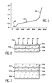
- the graph in FIG. 5 shows on the ordinate the bonding energy per unit area, between the structures bonded by molecular adhesion, as a function of the treatment temperature.
- the binding energies are expressed in J / m 2 and the temperatures in ° C.
- Regions 32, 33 and 34 of the curve of graph relate to second, third and fourth steps of the bonding process and correspond respectively to a hydrogen type interaction between water films, a hydrogen interaction between OH groups (reference 24) then a type interaction Si-O-Si.
- reference 24 a hydrogen interaction between OH groups
- Si-O-Si a type interaction between Si-O-Si.
- binding energies greater than 2 J / m 2 can be obtained. These energies are thus of the order of magnitude of the cohesion energies of the silicon material.
- the handle substrate is eliminated for example by running-in and / or by mechanical-chemical abrasion.
- the method of transferring a thin layer requires the sacrifice of a substrate handle for each thin layer treated. This sacrifice also represents a significant industrial cost.
- the object of the present invention is to provide a treatment for bonding two structures allowing, not only to obtain a collage very resistant molecular of the two structures but also allowing to take off the structures according to the bonding interface.
- An object of the invention is also to propose a treatment allowing a takeoff which does not damage assembled structures.
- the invention has more specifically for a processing method for the bonding of two structures by molecular adhesion according to a bonding interface, and takeoff of said two structures according to said interface of collage.
- thermal budget is meant, the sum of the heat treatments carried out and defined by a time / temperature pair applied to the structure.
- the heat treatment able to take off the two parts may take heat treatments into account before takeoff suffered by structures assemblies.
- a implantation of hydrogen in at least one of structures the hydrogen forming said element likely to diffuse in the structure.
- the implantation is carried out, for example, in silicon with a dose between 10 16 and 5.10 16 (H + / cm 2 ) and an energy between 20 and 500 KeV.
- the dose can be of the order of 3.10 16 ions / cm 2 and the implantation energy of the order of 70 KeV.
- the dose depends on the implantation conditions and in particular on the temperature of the structure during implantation.
- the heat treatment for takeoff can be carried out at a temperature between 600 and 1350 ° C. for example for silicon.
- this temperature is chosen rather of the order of 200 to 600 ° C.
- silicon carbide (S 1 C) the temperature is chosen from 600 ° C up to the melting temperature which is higher than 1350 ° C
- the heat treatment can take place, for example example, under heating lamps or in an oven.
- the structures to be assembled can be structures in one solid material but can also be multilayer structures containing areas that have been treated or not.
- the multilayer character of the structures can advantageously generate internal constraints which promote the separation of structures during the stage takeoff.
- FIG. 1 is a section schematic of a structure comprising a thin layer on a substrate, called the original substrate, assembled with another substrate, called handle substrate.
- FIG. 4 is a schematic section of a structure prepared for molecular bonding.
- FIG. 5 is a graph expressing the binding energy between two structures during stages of molecular bonding.
- FIG. 6 is a schematic section of a structure comprising a silicon wafer and illustrates the preparation of this structure for a molecular bonding according to the invention.
- Figure 7 shows in section the structure of Figure 6 pasted on another structure comprising a silicon wafer.
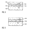
- FIG. 8 and 9 show in section the assembled structures of Figure 7, and illustrate a treatment stage for takeoff, in accordance with the invention.
- FIG. 10 shows in section another assembly obtained by molecular bonding of two structures according to the invention.
- FIG. 10 shows in section the assembly of FIG. 10 during a treatment for takeoff, according to the invention.
- FIG. 6 shows a structure 100 intended for molecular bonding in accordance with the invention.
- the structure 100 comprises a plate of silicon 102 covered with a layer of oxide of superficial silicon 104.
- An implanted hydrogen layer 106 is formed by implantation of hydrogen ions in the silicon plate 102 through the oxide layer 104.
- the hydrogen layer implanted at an energy of the order of 70 KeV, has , in this example, a concentration of 3.10 16 ions / cm 2 , a thickness of 400 nm and is buried at a depth of the order of 300 nm under the upper surface 110 of the structure 100. (The figures are not to scale and do not respect these proportions).
- hydrogen is meant the gaseous species constituted either in their atomic form (for example H) or in their molecular form (for example H 2 ) or in their ionic form (H + , H 2 + , ...) or in their isotopic (Deuterium) or isotopic and ionic form.
- the surface 110 of the structure 100 is then cleaned to make it hydrophilic and free of particles.
- a film of water (not shown in the figure) is formed on the surface 110.
- Low roughness can also be conferred or preserved on the surface 110 of the structure 100.
- the structure 100 is then assembled with a second structure 120.
- the second structure has a silicon wafer 122, whose surface in contact with the structure 100, also advantageously underwent cleaning for the make it hydrophilic.
- Reference 124 designates the interface between the structures 100 and 120 assembled.
- the structures then undergo a first annealing at a temperature of the order of 500 ° C. which allows to eliminate the layers of water between the structures assembled and which makes it possible to establish connections between the surfaces in contact.
- the bonding energy of the molecular bonding obtained at 500 ° C is of the order of 0.5 J / m 2 .
- Such a binding energy is sufficient, for example, to connect a silicon wafer containing integrated circuits to a handle substrate; it is in particular sufficient for all of the treatments envisaged for the wafer in the usual equipment for manufacturing microelectronic devices.
- the formation of the separation zones is controlled by the thermal budget applied to structures. Indeed, the heat treatment allows diffusing the hydrogen from the implanted layer 106 in the structure 100 towards the bonding interface 124. (Via oxide if present). The diffusing hydrogen is trapped at the interface 124, accumulates there and can evolve there under gaseous form. So the accumulation of hydrogen at the interface 124 makes it possible to counteract, at least in part, the bonding forces.
- diffusion of hydrogen towards interface 124 of collage is indicated by arrows 132.
- the detachment zones 130 can be local ( Figure 8) or extend over the entire interface surface (figure 9).
- the thermal budget necessary to obtain complete detachment depends on the quantity of the element liable to migrate present in the material of at least one of the structures.
- the thermal budget is therefore linked to the implantation dose of the hydrogen.
- the budget can be 900 ° C -30 min.
- Figure 10 shows another example of setting of the invention. It represents in section a assembly of a first structure 200 and a second structure 220 which are bonded by bonding molecular as previously described.
- the reference 224 designates the bonding interface between surfaces assembled structures.
- the first structure essentially comprises a silicon plate 202 on the surface of which formed a layer 206 of oxide.
- Layer oxide 206 is deposited by a channel deposition technique chemical vapor phase, plasma assisted (Plasma Enhanced Chemical Vapor Deposition). Such an oxide has peculiarity of containing OH molecules susceptible to broadcast.
- a first heat treatment, carried out at a temperature less than or equal to about 500 ° C allows to increase the energy of molecular bonding.
- the OH groups contained in the oxide layer 206 broadcast and migrate, notably to the interface 224 or they are trapped.
- the diffusion of OH groups towards the interface is indicated with arrows 232.
- the OH molecules evolve in gaseous form and are concentrated at the bonding interface. This phenomenon leads to bubble formation and induces embrittlement of the bonding interface.
- a detached area 230 is propagates until complete separation of the two structures 200 and 220.
- the separation of structures can be facilitated by the exercise of mechanical forces separation panels. These forces are represented by arrows 240, 241 in FIG. 11.
- the forces are 240 tensile forces and / or shear 241.
- the invention applies to any type of structure as defined above. It should be noted that the invention does not only relate to structures comprising silicon but also to other semiconductor structures (S i , S i C, A s G a ....), insulating structures (glass, quartz %) or even conductive structures (metal alloys ).
Abstract
Description
La présente invention concerne un procédé de traitement pour le collage par adhésion moléculaire et le décollage de deux structures.The present invention relates to a method of treatment for bonding by molecular adhesion and takeoff of two structures.
On entend par structure toute pièce de micromécanique, d'optique intégrée, ou de microélectronique susceptible d'être associée à une autre pièce par collage. Une telle structure peut être, par exemple, un substrat ou une plaque de support équipés ou non de composants électroniques, optiques ou mécaniques.By structure is meant any part of micromechanics, integrated optics, or microelectronics likely to be associated with a another piece by gluing. Such a structure can be, for example, a substrate or a support plate whether or not equipped with electronic, optical or mechanical.
Par ailleurs, le collage par adhésion moléculaire est compris comme un collage qui met en oeuvre une interaction entre les terminaisons chimiques présentes sur les surfaces des structures mises en contact.In addition, bonding by adhesion molecular is understood as a collage that highlights works an interaction between chemical terminations present on the surfaces of the structures contact.
L'invention trouve des applications notamment dans la fabrication de dispositifs à circuits intégrés. En effet, dans certains procédés de fabrication, les plaquettes de semi-conducteur contenant des circuits intégrés doivent être solidarisées avec des substrats de rigidité, puis désolidarisées en fin de traitement.The invention finds applications in particular in the manufacture of integrated circuit devices. Indeed, in certain manufacturing processes, the semiconductor wafers containing circuits integrated must be secured with substrates stiffness, then separated at the end of treatment.
Comme évoqué ci-dessus, et en particulier dans des applications de microélectronique concernant la fabrication de circuits de puissance, les tranches de semi-conducteur comportant des circuits électroniques intégrés se présentent sous la forme de plaquettes minces et de grandes dimensions. A titre d'exemple, on utilise des plaquettes d'un diamètre de quatre pouces (≃10cm) avec une épaisseur inférieure à 200 µm.As mentioned above, and in particular in microelectronics applications related to manufacturing of power circuits, the slices of semiconductor with electronic circuits integrated are in the form of plates thin and large. For example, we uses four inch diameter inserts (≃10cm) with a thickness less than 200 µm.
Les équipements standards de fabrication de dispositifs de microélectronique, tels que les photorépéteurs par exemple, ne sont pas adaptés au traitement de plaquettes aussi minces. De plus, les plaquettes de semi-conducteur minces présentent une grande fragilité. Cette fragilité est difficilement compatible avec des étapes de manipulation, et notamment de manipulation par des équipements de traitement automatisés.Standard manufacturing equipment microelectronics devices, such as photorepeaters for example, are not suitable for treatment of such thin platelets. Moreover, the thin semiconductor wafers exhibit a great fragility. This fragility is difficult compatible with handling steps, and including handling by automated processing.
Une plaquette mince ou une couche superficielle d'un substrat comportant ou non des circuits intégrés peut être collée sur un support de traitement encore appelé "substrat poignée". Le substrat poignée lui confère alors une résistance mécanique suffisante pour tous les traitements et manipulations envisagés.A thin wafer or surface layer a substrate with or without integrated circuits can be stuck on a processing medium again called "handle substrate". The handle substrate then provides sufficient mechanical strength to all the treatments and manipulations envisaged.
Les figures 1 à 3 annexées, décrites ci-après, illustrent à titre d'exemple un transfert d'une couche mince comprenant des circuits intégrés.Figures 1 to 3 attached, described below, illustrate as an example a transfer of a layer thin including integrated circuits.
La couche mince, repérée avec la référence 10
sur la figure 1, est initialement solidaire d'un
substrat 12, dit substrat d'origine. Elle comporte des
composants et des circuits électroniques intégrés non
représentés.The thin layer, identified with the
Le substrat d'origine 12 et la couche mince
superficielle 10 sont reportés sur un substrat poignée
14 en collant la couche mince superficielle sur le
substrat poignée. La structure ainsi obtenue est
représentée à la figure 1.The
Le substrat d'origine est ensuite éliminé par un procédé tel que la rectification ou le clivage, par attaque chimique et/ou par polissage pour obtenir la structure de la figure 2.The original substrate is then removed by a process such as rectification or cleavage, by chemical attack and / or polishing to obtain the structure of figure 2.
La couche mince 10 comprenant les circuits
intégrés, est désormais collée, à l'envers, sur le
substrat poignée 14. Le substrat poignée confère ainsi
à cette couche la rigidité nécessaire pour d'autres
opérations ou traitements de fabrication.The
Dans une dernière étape, représentée à la
figure 3, la couche mince 10 contenant les circuits
électroniques est transférée vers un substrat cible ou
substrat de destination 16 sur lequel elle est
définitivement fixée.In a final step, represented at
Figure 3, the
Après la fixation sur le substrat de
destination 16, la couche mince 10 est séparée du
substrat poignée 14. Aussi, le substrat poignée 14 est
représenté en trait discontinu sur la figure 3.After fixing on the
Un tel procédé est décrit de façon plus détaillée dans le document (1) dont la référence est indiquée à la fin de la présente description.Such a method is described more fully detailed in document (1) whose reference is indicated at the end of this description.
Le collage de la couche mince 10 sur le
substrat poignée 14 peut être effectué, par exemple, à
froid au moyen d'une colle appropriée. Le collage est
alors réversible et la séparation de la couche mince 10
du substrat poignée est possible. Toutefois, l'adhésion
obtenue entre la couche mince 10 et le substrat poignée
14 peut être insuffisante, notamment pour des
traitements ultérieurs à haute température. En
particulier, la colle n'est pas capable de supporter
des températures élevées.The bonding of the
De plus, la matière (colle) ajoutée pour le collage risque de provoquer une contamination métallique ou organique des pièces collées lors de traitements ultérieurs. In addition, the material (glue) added for the sticking may cause contamination metallic or organic parts glued during subsequent treatments.
Pour éviter ces inconvénients, on privilégie le collage par adhésion moléculaire qui ne met pas en oeuvre de colle ou de matière ajoutée. Le collage par adhésion moléculaire entre deux structures comporte pour l'essentiel quatre étapes qui sont indiquées ci-après.To avoid these drawbacks, we favor the bonding by molecular adhesion which does not glue or added material. The collage by molecular adhesion between two structures involves essentially four steps which are indicated below.
Une première étape comporte la préparation des surfaces des structures destinées à être mises en contact. L'obtention d'un collage moléculaire de qualité nécessite le contrôle de paramètres importants tels que la rugosité des surfaces, qui doit être de préférence inférieure à 0,5 nm (5Å), en valeur quadratique moyenne, l'absence de poussières (particules >0,2µm) sur les surfaces, la planéité des surfaces à mettre en contact et l'état chimique de ces surfaces.A first step involves the preparation of surfaces of structures intended to be contact. Obtaining a molecular collage of quality requires control of important parameters such as surface roughness, which must be preferably less than 0.5 nm (5Å), in value quadratic mean, the absence of dust (particles> 0.2µm) on the surfaces, the flatness of surfaces to be contacted and the chemical state of these surfaces.
La première étape comporte ainsi, pour l'essentiel, un nettoyage des surfaces des structures à coller afin d'en éliminer les particules étrangères et de rendre ces surfaces hydrophiles.The first step thus includes, for the essential, a cleaning of the surfaces of structures to stick in order to remove foreign particles and to make these surfaces hydrophilic.
La figure 4 montre une structure pour le
collage comportant un substrat de silicium 20 dont on a
rendu une surface 22 hydrophile. La surface 22 présente
une première couche hydrophile 24 constituée pour
l'essentiel de groupes chimiques Si-OH et une (ou
plusieurs) couche d'eau H2O 26 adsorbée sur la couche
hydrophile 24.FIG. 4 shows a structure for bonding comprising a
Une deuxième étape comporte la mise en contact des surfaces hydrophiles des deux structures à coller. Cette mise en contact permet de rapprocher suffisamment les couches d'eau adsorbées sur les structures pour que celles-ci entrent en interaction. L'attraction qui s'exerce entre les molécules d'eau se propage de proche en proche sur l'ensemble de la surface de chaque structure. Les surfaces en contact sont alors collées dans leur ensemble.A second step involves contacting hydrophilic surfaces of the two structures to be bonded. This contacting allows to bring sufficiently close the layers of water adsorbed on the structures so that these interact. The attraction that is exercised between water molecules spreads close in close on the entire surface of each structure. The contact surfaces are then glued in their whole.
La mesure de l'énergie du collage par une méthode d'insertion de lame donne une valeur de l'ordre de 0,15 J/m2. Une telle valeur est typiquement celle d'une adhésion de type hydrogène entre les deux couches d'eau, respectivement de chaque structure.The measurement of the bonding energy by a blade insertion method gives a value of the order of 0.15 J / m 2 . Such a value is typically that of a hydrogen type adhesion between the two layers of water, respectively of each structure.
Le document (2) dont la référence est indiquée à la fin de la présente description est cité comme une illustration de la méthode d'insertion de lame.The document (2) whose reference is indicated at the end of this description is cited as a illustration of the blade insertion method.
Une troisième étape comporte un traitement thermique de solidification de l'adhésion.A third step involves treatment thermal adhesion solidification.
Le traitement thermique permet, jusqu'à une température de l'ordre de 200°C, d'éliminer les couches d'eau entre les structures assemblées.The heat treatment allows, up to a temperature of the order of 200 ° C., removing the layers of water between the assembled structures.
L'adhésion des structures a alors lieu par des
liaisons de groupes OH, entre les couches de groupes
chimiques Si-OH respectivement de chaque structure. On
rappelle que la couche de groupes Si-OH est indiquée
avec la référence 24 sur la figure 4. De cette
interaction résulte une diminution de la distance des
deux structures en contact et la mise en interaction de
groupes OH supplémentaires. L'énergie du collage
augmente ainsi pour des températures de traitement de
200°C à 900°C.The adhesion of the structures then takes place by
OH group bonds, between group layers
Si-OH chemicals of each structure respectively. We
reminds that the layer of Si-OH groups is indicated
with the
Enfin, une éventuelle quatrième étape comprend un traitement thermique à plus de 900°C. Lors de cette étape, les groupes Si-OH en interaction évoluent vers des liaisons de type Si-O-Si, beaucoup plus fortes. On observe alors une très forte augmentation de l'énergie de liaison. Finally, a possible fourth step includes heat treatment above 900 ° C. During this step, the interacting Si-OH groups evolve towards much stronger Si-O-Si bonds. We then observe a very strong increase in energy link.
Le graphique de la figure 5 indique en ordonnée l'énergie de liaison par unité de surface, entre les structures collées par adhésion moléculaire, en fonction de la température de traitement. Les énergies de liaison sont exprimées en J/m2 et les températures en °C.The graph in FIG. 5 shows on the ordinate the bonding energy per unit area, between the structures bonded by molecular adhesion, as a function of the treatment temperature. The binding energies are expressed in J / m 2 and the temperatures in ° C.
Des régions 32, 33 et 34 de la courbe du
graphique se rapportent aux deuxième, troisième et
quatrième étapes du procédé de collage et correspondent
respectivement à une interaction de type hydrogène
entre les films d'eau, une interaction hydrogène entre
groupes OH (référence 24) puis une interaction de type
Si-O-Si. Une description plus détaillée du collage de
plaquettes de silicium peut être trouvée dans le
document (3) dont la référence est indiquée à la fin de
la présente description.
On peut noter que pour des températures de traitement supérieures à 600°C, il devient impossible de redécoller les deux structures assemblées sans leur faire subir des dégradations importantes.It can be noted that for temperatures of treatment above 600 ° C, it becomes impossible to relaunch the two assembled structures without their subject significant degradations.
Lorsque les structures assemblées sont des plaquettes de silicium, des énergies de liaison supérieures à 2 J/m2 peuvent être obtenues. Ces énergies sont ainsi de l'ordre de grandeur des énergies de cohésion du matériau silicium.When the assembled structures are silicon wafers, binding energies greater than 2 J / m 2 can be obtained. These energies are thus of the order of magnitude of the cohesion energies of the silicon material.
Il apparaít immédiatement que si un collage moléculaire est mis en oeuvre dans un procédé de transfert tel qu'illustré par les figures 1 à 3, il est impossible de détacher le substrat poignée de la couche mince par des forces mécaniques, sans détruire la couche mince ou le substrat poignée.It immediately appears that if a collage molecular is implemented in a process of transfer as illustrated in Figures 1 to 3, it is impossible to detach the handle substrate from the layer thin by mechanical forces, without destroying the thin layer or handle substrate.
Ainsi, la séparation de la couche mince du substrat poignée a lieu par élimination du substrat poignée. Le substrat poignée est éliminé par exemple par rodage et/ou par abrasion mécano-chimique.So the separation of the thin layer of the substrate handle takes place by removal of the substrate handle. The handle substrate is eliminated for example by running-in and / or by mechanical-chemical abrasion.
Dans ce cas, le procédé de transfert d'une couche mince nécessite le sacrifice d'un substrat poignée pour chaque couche mince traitée. Ce sacrifice représente également un coût industriel important.In this case, the method of transferring a thin layer requires the sacrifice of a substrate handle for each thin layer treated. This sacrifice also represents a significant industrial cost.
La présente invention a pour but de proposer un traitement pour le collage de deux structures permettant, non seulement d'obtenir un collage moléculaire très résistant des deux structures, mais permettant également de décoller les structures selon l'interface de collage.The object of the present invention is to provide a treatment for bonding two structures allowing, not only to obtain a collage very resistant molecular of the two structures but also allowing to take off the structures according to the bonding interface.
Un but de l'invention est également de proposer un traitement permettant un décollage qui n'abíme pas les structures assemblées.An object of the invention is also to propose a treatment allowing a takeoff which does not damage assembled structures.
Pour atteindre ces buts, l'invention a plus précisément pour objet un procédé de traitement pour le collage de deux structures par adhésion moléculaire selon une interface de collage, et le décollage desdites deux structures selon ladite interface de collage.To achieve these goals, the invention has more specifically for a processing method for the bonding of two structures by molecular adhesion according to a bonding interface, and takeoff of said two structures according to said interface of collage.
Conformément à l'invention,
- on utilise, pour le collage, au moins une structure contenant au moins un élément susceptible de diffuser dans ladite structure vers l'interface de collage, et
- on effectue, pour le décollage, un traitement thermique avec un budget thermique suffisant pour faire diffuser ledit élément vers l'interface de collage pour la fragiliser.
- at least one structure containing at least one element capable of diffusing into said structure towards the bonding interface is used for bonding, and
- heat take-off is carried out for take-off with a thermal budget sufficient to cause said element to diffuse towards the bonding interface in order to weaken it.
On entend par élément susceptible de diffuser tout élément, simple ou composé, présent intrinsèquement ou incorporé, volontairement ou involontairement, dans le matériau, capable de migrer dans le matériau vers l'interface de collage, pour réagir avec celui-ci. Cet élément est alors apte à modifier cet interface au cours du traitement thermique et à conduire à la séparation des deux parties de part et d'autre de l'interface. Cette séparation peut être assistée par une phase gazeuse qui se forme éventuellement à l'interface au cours du traitement thermique.By element likely to diffuse any element, simple or compound, present intrinsically or incorporated, voluntarily or involuntarily, in the material, able to migrate in the material towards the bonding interface, to react with it. This element is then suitable for modify this interface during heat treatment and lead to the separation of the two parts of share on the other side of the interface. This separation can be assisted by a gaseous phase which forms possibly at the interface during processing thermal.
Par ailleurs, on entend par budget thermique, la somme des traitements thermiques effectués et définis par un couple temps/température appliqué à la structure.Furthermore, by thermal budget is meant, the sum of the heat treatments carried out and defined by a time / temperature pair applied to the structure.
Ainsi, le traitement thermique apte à décoller les deux parties (de part et d'autre de l'interface de collage) peut tenir compte de traitements thermiques antérieurs au décollage subis par les structures assemblées.Thus, the heat treatment able to take off the two parts (on either side of the interface of bonding) may take heat treatments into account before takeoff suffered by structures assemblies.
Selon une mise en oeuvre particulière du procédé, on peut effectuer, avant le collage, une implantation d'hydrogène dans au moins l'une des structures, l'hydrogène formant ledit élément susceptible de diffuser dans la structure.According to a particular implementation of the process, before bonding, a implantation of hydrogen in at least one of structures, the hydrogen forming said element likely to diffuse in the structure.
L'implantation est effectuée, par exemple, dans du silicium avec une dose comprise entre 1016 et 5.1016 (H+/cm2) et une énergie comprise entre 20 et 500 KeV. De préférence, la dose peut être de l'ordre de 3.1016 ions/cm2 et l'énergie d'implantation de l'ordre de 70 KeV. La dose dépend des conditions d'implantation et en particulier de la température de la structure pendant l'implantation. The implantation is carried out, for example, in silicon with a dose between 10 16 and 5.10 16 (H + / cm 2 ) and an energy between 20 and 500 KeV. Preferably, the dose can be of the order of 3.10 16 ions / cm 2 and the implantation energy of the order of 70 KeV. The dose depends on the implantation conditions and in particular on the temperature of the structure during implantation.
Selon une variante, on peut aussi utiliser au moins une structure comprenant une couche superficielle d'oxyde formée par un dépôt chimique en phase vapeur assisté par plasma et contenant des molécules OH, lesdites molécules OH formant l'élément susceptible de diffuser.Alternatively, one can also use at less a structure comprising a surface layer of oxide formed by chemical vapor deposition assisted by plasma and containing OH molecules, said OH molecules forming the element capable of broadcast.
Le traitement thermique pour le décollage peut être effectué à une température comprise entre 600 et 1 350°C par exemple pour le silicium. Pour de l'arséniure de gallium (AsGa) cette température est choisie plutôt de l'ordre de 200 à 600°C. Pour le carbure de silicium (S1C) la température est choisie de 600°C jusqu'à la température de fusion qui est supérieure à 1 350°CThe heat treatment for takeoff can be carried out at a temperature between 600 and 1350 ° C. for example for silicon. For gallium arsenide (A s G a ) this temperature is chosen rather of the order of 200 to 600 ° C. For silicon carbide (S 1 C) the temperature is chosen from 600 ° C up to the melting temperature which is higher than 1350 ° C
Le traitement thermique peut avoir lieu, par exemple, sous des lampes de chauffage ou dans un four.The heat treatment can take place, for example example, under heating lamps or in an oven.
Les structures à assembler peuvent être des structures en un seul matériau massif mais peuvent aussi être des structures multicouches contenant des zones ayant été traitées ou pas.The structures to be assembled can be structures in one solid material but can also be multilayer structures containing areas that have been treated or not.
Le caractère multicouche des structures peut avantageusement engendrer des contraintes internes qui favorisent la séparation des structures lors de l'étape de décollage.The multilayer character of the structures can advantageously generate internal constraints which promote the separation of structures during the stage takeoff.
De la même façon, on peut préparer, avant le collage, la surface d'au moins une des structures à assembler pour y pratiquer un relief. Ce relief permet également de faciliter la séparation des structures lors du décollage.In the same way, one can prepare, before the bonding, the surface of at least one of the structures to assemble to practice a relief. This relief allows also to facilitate the separation of structures during takeoff.
Enfin, pour favoriser encore le décollage, on peut exercer sur les structures des forces extérieures de séparation. Il s'agit, par exemple, de forces de traction ou de flexion exercées sur les structures ou encore des forces de cisaillement provoquées par l'insertion d'une lame au niveau de l'interface entre les structures.Finally, to further promote takeoff, we can exert on external force structures of seperation. These are, for example, traction or bending exerted on structures or still shear forces caused by the insertion of a blade at the interface between the structures.
D'autres caractéristiques et avantages de l'invention ressortiront mieux de la description qui va suivre, en référence aux figures des dessins annexés. Cette description est donnée à titre purement illustratif et non limitatif.Other features and benefits of the invention will emerge better from the description which goes follow, with reference to the figures in the accompanying drawings. This description is given purely illustrative and not limiting.
- La figure 1, déjà décrite, est une coupe schématique d'une structure comprenant une couche mince sur un substrat, dit substrat d'origine, assemblée avec un autre substrat, dit substrat poignée.- Figure 1, already described, is a section schematic of a structure comprising a thin layer on a substrate, called the original substrate, assembled with another substrate, called handle substrate.
- La figure 2, déjà décrite, est une coupe schématique du substrat poignée sur lequel est collée la couche mince.- Figure 2, already described, is a section schematic of the handle substrate on which is glued the thin layer.
- La figure 3, déjà décrite, est une coupe schématique de la couche mince reportée sur un substrat dit substrat de destination.- Figure 3, already described, is a section schematic of the thin layer transferred onto a substrate said destination substrate.
- La figure 4 est une coupe schématique d'une structure préparée pour un collage moléculaire.- Figure 4 is a schematic section of a structure prepared for molecular bonding.
- La figure 5 est un graphique exprimant l'énergie de liaison entre deux structures lors des étapes d'un collage moléculaire.- Figure 5 is a graph expressing the binding energy between two structures during stages of molecular bonding.
- La figure 6 est une coupe schématique d'une structure comprenant une plaquette de silicium et illustre la préparation de cette structure pour un collage moléculaire conforme à l'invention.- Figure 6 is a schematic section of a structure comprising a silicon wafer and illustrates the preparation of this structure for a molecular bonding according to the invention.
- La figure 7 montre en coupe la structure de la figure 6 collée sur une autre structure comprenant une plaquette de silicium. - Figure 7 shows in section the structure of Figure 6 pasted on another structure comprising a silicon wafer.
- Les figures 8 et 9 montrent en coupe les structures assemblées de la figure 7, et illustrent une étape de traitement pour le décollage, conforme à l'invention.- Figures 8 and 9 show in section the assembled structures of Figure 7, and illustrate a treatment stage for takeoff, in accordance with the invention.
- La figure 10 montre en coupe un autre assemblage obtenu par collage moléculaire de deux structures, conformément à l'invention.- Figure 10 shows in section another assembly obtained by molecular bonding of two structures according to the invention.
- La figure 11 montre en coupe l'assemblage de la figure 10 lors d'un traitement pour le décollage, conformément à l'invention.- Figure 11 shows in section the assembly of FIG. 10 during a treatment for takeoff, according to the invention.
La figure 6 montre une structure 100 destinée à
un collage par adhésion moléculaire conforme à
l'invention.FIG. 6 shows a
La structure 100 comporte une plaque de
silicium 102 recouverte d'une couche d'oxyde de
silicium superficielle 104.The
Une couche d'hydrogène 106 implantée, est
formée par implantation d'ions hydrogène dans la plaque
de silicium 102 à travers la couche d'oxyde 104. La
couche d'hydrogène, implantée à une énergie de l'ordre
de 70 KeV, présente, dans cet exemple, une
concentration de 3.1016 ions/cm2, une épaisseur de
400 nm et est enterrée à une profondeur de l'ordre de
300 nm sous la surface supérieure 110 de la structure
100. (Les figures ne sont pas à l'échelle et ne
respectent pas ces proportions).An implanted
Par hydrogène, on entend les espèces gazeuses constituées soit sous leur forme atomique (par exemple H) ou sous leur forme moléculaire (par exemple H2) ou sous leur forme ionique (H+, H2 +,... ) ou sous leur forme isotopique (Deutérium) ou isotopique et ionique.By hydrogen is meant the gaseous species constituted either in their atomic form (for example H) or in their molecular form (for example H 2 ) or in their ionic form (H + , H 2 + , ...) or in their isotopic (Deuterium) or isotopic and ionic form.
Si nécessaire, la surface 110 de la structure
100 est ensuite nettoyée afin de la rendre hydrophile
et exempte de particules. Un film d'eau (non représenté
sur la figure) est formé sur la surface 110.If necessary, the
Une faible rugosité peut également être
conférée ou conservée à la surface 110 de la structure
100.Low roughness can also be
conferred or preserved on the
Comme le montre la figure 7, la structure 100
est ensuite assemblée avec une deuxième structure 120.
La deuxième structure comporte une plaque de silicium
122, dont la surface en contact avec la structure 100,
a également avantageusement subi un nettoyage pour la
rendre hydrophile.As shown in Figure 7, the
La référence 124 désigne l'interface entre les
structures 100 et 120 assemblées.
Les structures subissent ensuite un premier recuit à une température de l'ordre de 500°C qui permet d'éliminer les couches d'eau entre les structures assemblées et qui permet d'établir des liaisons moléculaires entre les surfaces en contact.The structures then undergo a first annealing at a temperature of the order of 500 ° C. which allows to eliminate the layers of water between the structures assembled and which makes it possible to establish connections between the surfaces in contact.
L'énergie de liaison du collage moléculaire obtenu à 500°C est de l'ordre de 0,5J/m2. Une telle énergie de liaison est suffisante, par exemple, pour relier une plaquette de silicium contenant des circuits intégrés à un substrat poignée ; elle est notamment suffisante pour l'ensemble des traitements envisagés pour la plaquette dans les équipements usuels de fabrication de dispositifs de microélectronique.The bonding energy of the molecular bonding obtained at 500 ° C is of the order of 0.5 J / m 2 . Such a binding energy is sufficient, for example, to connect a silicon wafer containing integrated circuits to a handle substrate; it is in particular sufficient for all of the treatments envisaged for the wafer in the usual equipment for manufacturing microelectronic devices.
Lorsqu'on prolonge le traitement thermique ou
lorsqu'on effectue un nouveau traitement thermique à
une température de l'ordre de 800°C, ou plus, des zones
de décollement, indiquées avec la référence 130 sur les
figures 8 et 9, apparaissent au niveau de l'interface
124 entre les structures 100 et 120 assemblées.When extending the heat treatment or
when performing a new heat treatment at
a temperature of the order of 800 ° C., or more, of the zones
of separation, indicated with the
La formation des zones de décollement est
contrôlée par le budget thermique appliqué aux
structures. En effet, le traitement thermique permet de
faire diffuser l'hydrogène de la couche 106 implantée
dans la structure 100 vers l'interface 124 de collage.
(Par l'intermédiaire de l'oxyde s'il est présent).
L'hydrogène qui diffuse est piégé au niveau de
l'interface 124, s'y accumule et peut y évoluer sous
forme gazeuse. Ainsi, l'accumulation de l'hydrogène à
l'interface 124 permet de contrecarrer, au moins en
partie, les forces de collage. Sur les figures 8 et 9
la diffusion de l'hydrogène vers l'interface 124 de
collage est indiquée par des flèches 132.The formation of the separation zones is
controlled by the thermal budget applied to
structures. Indeed, the heat treatment allows
diffusing the hydrogen from the implanted
Selon l'importance du budget thermique mis en
oeuvre, les zones de décollement 130 peuvent être
locales (figure 8) ou s'étendre sur l'ensemble de la
surface de l'interface (figure 9).Depending on the size of the thermal budget
work, the
Le budget thermique nécessaire à l'obtention du décollement complet dépend de la quantité de l'élément susceptible de migrer présent dans le matériau d'au moins l'une des structures. Dans le présent exemple, le budget thermique est par conséquent lié à la dose d'implantation de l'hydrogène. A titre d'exemple pour une dose de 3.166 cm3 le budget peut être de 900°C -30 min.The thermal budget necessary to obtain complete detachment depends on the quantity of the element liable to migrate present in the material of at least one of the structures. In the present example, the thermal budget is therefore linked to the implantation dose of the hydrogen. For example, for a dose of 3.16 6 cm 3 the budget can be 900 ° C -30 min.
La figure 10 indique un autre exemple de mise
en oeuvre de l'invention. Elle représente en coupe un
assemblage d'une première structure 200 et d'une
deuxième structure 220 qui sont collées par un collage
moléculaire tel que décrit précédemment. La référence
224 désigne l'interface de collage entre les surfaces
des structures assemblées.Figure 10 shows another example of setting
of the invention. It represents in section a
assembly of a
La première structure comporte pour l'essentiel
une plaque de silicium 202 à la surface de laquelle on
a formé une couche 206 d'oxyde. L'oxyde de la couche
206 est déposé par une technique de dépôt par voie
chimique en phase vapeur, assistée par plasma (Plasma
Enhanced Chemical Vapor Deposition). Un tel oxyde a la
particularité de contenir des molécules OH susceptibles
de diffuser.The first structure essentially comprises
a
Un premier traitement thermique, effectué à une température inférieure ou égale à environ 500°C permet d'augmenter l'énergie du collage moléculaire.A first heat treatment, carried out at a temperature less than or equal to about 500 ° C allows to increase the energy of molecular bonding.
Lorsque le traitement thermique est poursuivi
ou repris à des températures supérieures à 500°C
environ, les groupes OH contenus dans la couche d'oxyde
206 diffusent et migrent, notamment vers l'interface
224 ou ils sont piégés. La diffusion des groupes OH
vers l'interface est indiquée avec des flèches 232.When heat treatment is continued
or taken up at temperatures above 500 ° C
approximately, the OH groups contained in the
A l'interface 224, les molécules OH évoluent sous forme gazeuse et se concentrent au niveau de l'interface de collage. Ce phénomène entraíne la formation de bulles et induit une fragilisation de l'interface de collage.At the 224 interface, the OH molecules evolve in gaseous form and are concentrated at the bonding interface. This phenomenon leads to bubble formation and induces embrittlement of the bonding interface.
Sous l'effet d'une pression générée par le gaz,
une zone décollée 230, représentée à la figure 11, se
propage jusqu'au décollement complet des deux
structures 200 et 220. La séparation des structures
peut être facilité par l'exercice de forces mécaniques
de séparation extérieures. Ces forces sont représentées
par des flèches 240, 241 sur la figure 11. Les forces
sont des forces de traction 240 et/ou des forces de
cisaillement 241.Under the effect of a pressure generated by the gas,
a
Il apparaít ainsi que le procédé de l'invention peut être notamment mis à profit pour le collage moléculaire de plaquettes de circuits intégrés, sans ajout de matière, tout en autorisant une réversibilité du collage.It thus appears that the method of the invention can be used in particular for bonding molecular circuit board, without addition of material, while allowing reversibility collage.
Par ailleurs, l'invention s'applique à tout type de structure tel que défini précédemment. Il convient de préciser que l'invention ne concerne pas uniquement des structures comportant du silicium mais aussi d'autres structures semi-conductrices (Si, SiC, AsGa....), des structures isolantes (verre, quartz...) ou même des structures conductrices (alliages métalliques...).Furthermore, the invention applies to any type of structure as defined above. It should be noted that the invention does not only relate to structures comprising silicon but also to other semiconductor structures (S i , S i C, A s G a ....), insulating structures (glass, quartz ...) or even conductive structures (metal alloys ...).
W.P. Maszara, G. Goetz, A. Caviglia and J.B. McKitterick
Aerospace Technology Center, Allied Signal Aerospace Company, Columbia, Maryland 21045
(Received 12 April 1988, accepted for publication 28 July 1988). (2) "Bonding of silicon wafers for silicon-on-insulator"
WP Maszara, G. Goetz, A. Caviglia and JB McKitterick
Aerospace Technology Center, Allied Signal Aerospace Company, Columbia, Maryland 21045
(Received 12 April 1988, accepted for publication 28 July 1988).
R. Stengl, T. Tan and U. Gösele
School of Engineering, Duke University, Durham, North Carolina 27706, USA
(Received May 8, 1989, accepted for publication July 15, 1989).
Japanese Journal of Applied Physics, vol. 28, N°10, October 1989, pp. 1735-1741. (3) "A model for the silicon wafer bonding process"
R. Stengl, T. Tan and U. Gösele
School of Engineering, Duke University, Durham, North Carolina 27706, USA
(Received May 8, 1989, accepted for publication July 15, 1989).
Japanese Journal of Applied Physics, vol. 28, N ° 10, October 1989, pp. 1735-1741.
Claims (10)
Applications Claiming Priority (2)
| Application Number | Priority Date | Filing Date | Title |
|---|---|---|---|
| FR9710480A FR2767604B1 (en) | 1997-08-19 | 1997-08-19 | TREATMENT PROCESS FOR MOLECULAR GLUING AND TAKING OFF TWO STRUCTURES |
| FR9710480 | 1997-08-19 |
Publications (2)
| Publication Number | Publication Date |
|---|---|
| EP0898307A1 true EP0898307A1 (en) | 1999-02-24 |
| EP0898307B1 EP0898307B1 (en) | 2006-12-27 |
Family
ID=9510376
Family Applications (1)
| Application Number | Title | Priority Date | Filing Date |
|---|---|---|---|
| EP98402073A Expired - Lifetime EP0898307B1 (en) | 1997-08-19 | 1998-08-17 | Method of treatment for molecular gluing and ungluing of two structures |
Country Status (5)
| Country | Link |
|---|---|
| US (1) | US6429094B1 (en) |
| EP (1) | EP0898307B1 (en) |
| JP (1) | JP4316701B2 (en) |
| DE (1) | DE69836707T2 (en) |
| FR (1) | FR2767604B1 (en) |
Cited By (10)
| Publication number | Priority date | Publication date | Assignee | Title |
|---|---|---|---|---|
| EP1187216A1 (en) * | 1999-12-24 | 2002-03-13 | Shin-Etsu Handotai Company, Limited | Method for manufacturing bonded wafer |
| FR2835095A1 (en) * | 2002-01-22 | 2003-07-25 | Soitec Silicon On Insulator | PROCESS FOR THE PREPARATION OF SEPARABLE SEMICONDUCTOR ASSEMBLIES, IN PARTICULAR FOR FORMING SUBSTRATES FOR ELECTRONICS, OPTOELECTRICS AND OPTICS |
| FR2926672A1 (en) * | 2008-01-21 | 2009-07-24 | Soitec Silicon On Insulator | PROCESS FOR MANUFACTURING LAYERS OF EPITAXY MATERIAL |
| US7902038B2 (en) * | 2001-04-13 | 2011-03-08 | Commissariat A L'energie Atomique | Detachable substrate with controlled mechanical strength and method of producing same |
| US8048766B2 (en) | 2003-06-24 | 2011-11-01 | Commissariat A L'energie Atomique | Integrated circuit on high performance chip |
| US8252663B2 (en) | 2009-06-18 | 2012-08-28 | Commissariat A L'energie Atomique Et Aux Energies Alternatives | Method of transferring a thin layer onto a target substrate having a coefficient of thermal expansion different from that of the thin layer |
| US8309431B2 (en) | 2003-10-28 | 2012-11-13 | Commissariat A L'energie Atomique | Method for self-supported transfer of a fine layer by pulsation after implantation or co-implantation |
| US8389379B2 (en) | 2002-12-09 | 2013-03-05 | Commissariat A L'energie Atomique | Method for making a stressed structure designed to be dissociated |
| US8609514B2 (en) | 1997-12-10 | 2013-12-17 | Commissariat A L'energie Atomique | Process for the transfer of a thin film comprising an inclusion creation step |
| FR3029538A1 (en) * | 2014-12-04 | 2016-06-10 | Soitec Silicon On Insulator | LAYER TRANSFER METHOD |
Families Citing this family (30)
| Publication number | Priority date | Publication date | Assignee | Title |
|---|---|---|---|---|
| FR2774511B1 (en) * | 1998-01-30 | 2002-10-11 | Commissariat Energie Atomique | SUBSTRATE COMPLIANT IN PARTICULAR FOR A DEPOSIT BY HETERO-EPITAXY |
| FR2815121B1 (en) * | 2000-10-06 | 2002-12-13 | Commissariat Energie Atomique | PROCESS FOR REVELATION OF CRYSTALLINE DEFECTS AND / OR STRESS FIELDS AT THE MOLECULAR ADHESION INTERFACE OF TWO SOLID MATERIALS |
| JP2002270553A (en) * | 2001-03-13 | 2002-09-20 | Mitsubishi Gas Chem Co Inc | Manufacturing method of electronic component |
| FR2823596B1 (en) * | 2001-04-13 | 2004-08-20 | Commissariat Energie Atomique | SUBSTRATE OR DISMOUNTABLE STRUCTURE AND METHOD OF MAKING SAME |
| FR2837981B1 (en) * | 2002-03-28 | 2005-01-07 | Commissariat Energie Atomique | PROCESS FOR HANDLING SEMICONDUCTOR LAYERS FOR THEIR SLOWDOWN |
| JP4277481B2 (en) * | 2002-05-08 | 2009-06-10 | 日本電気株式会社 | Semiconductor substrate manufacturing method and semiconductor device manufacturing method |
| FR2856192B1 (en) * | 2003-06-11 | 2005-07-29 | Soitec Silicon On Insulator | METHOD FOR PRODUCING HETEROGENEOUS STRUCTURE AND STRUCTURE OBTAINED BY SUCH A METHOD |
| FR2857953B1 (en) | 2003-07-21 | 2006-01-13 | Commissariat Energie Atomique | STACKED STRUCTURE, AND METHOD FOR MANUFACTURING THE SAME |
| FR2860178B1 (en) * | 2003-09-30 | 2005-11-04 | Commissariat Energie Atomique | METHOD OF SEPARATING GLUE PLATES BETWEEN THEM TO CONSTITUTE A STACKED STRUCTURE. |
| US7608520B2 (en) * | 2003-11-06 | 2009-10-27 | Panasonic Corporation | Method for bonding substrate, bonded substrate, and direct bonded substrate |
| FR2880189B1 (en) * | 2004-12-24 | 2007-03-30 | Tracit Technologies Sa | METHOD FOR DEFERRING A CIRCUIT ON A MASS PLAN |
| FR2889887B1 (en) | 2005-08-16 | 2007-11-09 | Commissariat Energie Atomique | METHOD FOR DEFERING A THIN LAYER ON A SUPPORT |
| JP4830418B2 (en) * | 2005-09-16 | 2011-12-07 | 株式会社デンソー | Semiconductor device |
| FR2891281B1 (en) | 2005-09-28 | 2007-12-28 | Commissariat Energie Atomique | METHOD FOR MANUFACTURING A THIN FILM ELEMENT |
| FR2903808B1 (en) * | 2006-07-11 | 2008-11-28 | Soitec Silicon On Insulator | PROCESS FOR DIRECTLY BONDING TWO SUBSTRATES USED IN ELECTRONIC, OPTICAL OR OPTOELECTRONIC |
| US8124499B2 (en) * | 2006-11-06 | 2012-02-28 | Silicon Genesis Corporation | Method and structure for thick layer transfer using a linear accelerator |
| US20080128641A1 (en) * | 2006-11-08 | 2008-06-05 | Silicon Genesis Corporation | Apparatus and method for introducing particles using a radio frequency quadrupole linear accelerator for semiconductor materials |
| FR2910179B1 (en) | 2006-12-19 | 2009-03-13 | Commissariat Energie Atomique | METHOD FOR MANUFACTURING THIN LAYERS OF GaN BY IMPLANTATION AND RECYCLING OF A STARTING SUBSTRATE |
| US20080188011A1 (en) * | 2007-01-26 | 2008-08-07 | Silicon Genesis Corporation | Apparatus and method of temperature conrol during cleaving processes of thick film materials |
| FR2925221B1 (en) | 2007-12-17 | 2010-02-19 | Commissariat Energie Atomique | METHOD FOR TRANSFERRING A THIN LAYER |
| FR2926674B1 (en) | 2008-01-21 | 2010-03-26 | Soitec Silicon On Insulator | METHOD FOR MANUFACTURING COMPOSITE STRUCTURE WITH STABLE BONDING OXIDE LAYER |
| FR2926748B1 (en) * | 2008-01-25 | 2010-04-02 | Commissariat Energie Atomique | OBJECT PROVIDED WITH A GRAPHIC ELEMENT REPORTED ON A SUPPORT AND METHOD OF MAKING SUCH AN OBJECT. |
| FR2931014B1 (en) * | 2008-05-06 | 2010-09-03 | Soitec Silicon On Insulator | METHOD OF ASSEMBLING PLATES BY MOLECULAR ADHESION |
| FR2938117B1 (en) * | 2008-10-31 | 2011-04-15 | Commissariat Energie Atomique | METHOD FOR PRODUCING A HYBRID SUBSTRATE HAVING AN ELECTRICALLY INSULATING CONTINUOUS LAYER BURIED |
| US7927975B2 (en) | 2009-02-04 | 2011-04-19 | Micron Technology, Inc. | Semiconductor material manufacture |
| JP5524776B2 (en) * | 2010-09-10 | 2014-06-18 | 日本電信電話株式会社 | Thin film forming method and sheet film |
| US8524572B2 (en) * | 2011-10-06 | 2013-09-03 | Micron Technology, Inc. | Methods of processing units comprising crystalline materials, and methods of forming semiconductor-on-insulator constructions |
| CN104507853B (en) | 2012-07-31 | 2016-11-23 | 索泰克公司 | The method forming semiconductor equipment |
| FR3077924B1 (en) * | 2018-02-13 | 2020-01-17 | Soitec | REMOVABLE STRUCTURE AND DISASSEMBLY METHOD USING THE SAME |
| FR3079532B1 (en) * | 2018-03-28 | 2022-03-25 | Soitec Silicon On Insulator | METHOD FOR MANUFACTURING A MONOCRYSTALLINE LAYER OF AIN MATERIAL AND SUBSTRATE FOR GROWTH BY EPITAXIS OF A MONOCRYSTALLINE LAYER OF AIN MATERIAL |
Citations (3)
| Publication number | Priority date | Publication date | Assignee | Title |
|---|---|---|---|---|
| FR2501907A1 (en) * | 1981-03-13 | 1982-09-17 | Thomson Csf | Molecular adhesion plane substrate holder - takes any sized substrate held on plate by copolymer elastomer and resin layer pressed in place and removed by fluid pressure |
| WO1994017551A1 (en) * | 1993-01-19 | 1994-08-04 | Hughes Aircraft Company | Intermediate-temperature diffusion welding |
| EP0751556A1 (en) * | 1995-06-30 | 1997-01-02 | Commissariat A L'energie Atomique | Fabrication process for an interconnection substrate allowing to connect a die to a carrier substrate |
Family Cites Families (5)
| Publication number | Priority date | Publication date | Assignee | Title |
|---|---|---|---|---|
| US5503704A (en) * | 1993-01-06 | 1996-04-02 | The Regents Of The University Of California | Nitrogen based low temperature direct bonding |
| US5310451A (en) * | 1993-08-19 | 1994-05-10 | International Business Machines Corporation | Method of forming an ultra-uniform silicon-on-insulator layer |
| US5510277A (en) * | 1994-06-29 | 1996-04-23 | At&T Corp. | Surface treatment for silicon substrates |
| DE19648501A1 (en) * | 1996-11-22 | 1998-05-28 | Max Planck Gesellschaft | Method for removable connection and finally separation of reversibly bonded and polished plates |
| US5882987A (en) * | 1997-08-26 | 1999-03-16 | International Business Machines Corporation | Smart-cut process for the production of thin semiconductor material films |
-
1997
- 1997-08-19 FR FR9710480A patent/FR2767604B1/en not_active Expired - Lifetime
-
1998
- 1998-08-11 US US09/132,059 patent/US6429094B1/en not_active Expired - Lifetime
- 1998-08-17 DE DE69836707T patent/DE69836707T2/en not_active Expired - Lifetime
- 1998-08-17 EP EP98402073A patent/EP0898307B1/en not_active Expired - Lifetime
- 1998-08-19 JP JP23326898A patent/JP4316701B2/en not_active Expired - Lifetime
Patent Citations (3)
| Publication number | Priority date | Publication date | Assignee | Title |
|---|---|---|---|---|
| FR2501907A1 (en) * | 1981-03-13 | 1982-09-17 | Thomson Csf | Molecular adhesion plane substrate holder - takes any sized substrate held on plate by copolymer elastomer and resin layer pressed in place and removed by fluid pressure |
| WO1994017551A1 (en) * | 1993-01-19 | 1994-08-04 | Hughes Aircraft Company | Intermediate-temperature diffusion welding |
| EP0751556A1 (en) * | 1995-06-30 | 1997-01-02 | Commissariat A L'energie Atomique | Fabrication process for an interconnection substrate allowing to connect a die to a carrier substrate |
Non-Patent Citations (1)
| Title |
|---|
| MASZARA W P ET AL: "BONDING OF SILICON WAFERS FOR SILICON-ON-INSULATOR", JOURNAL OF APPLIED PHYSICS, vol. 64, no. 10, PART 1, 15 November 1988 (1988-11-15), pages 4943 - 4950, XP000050002 * |
Cited By (21)
| Publication number | Priority date | Publication date | Assignee | Title |
|---|---|---|---|---|
| US8609514B2 (en) | 1997-12-10 | 2013-12-17 | Commissariat A L'energie Atomique | Process for the transfer of a thin film comprising an inclusion creation step |
| EP1187216A4 (en) * | 1999-12-24 | 2008-09-24 | Shinetsu Handotai Kk | Method for manufacturing bonded wafer |
| US6566233B2 (en) | 1999-12-24 | 2003-05-20 | Shin-Etsu Handotai Co., Ltd. | Method for manufacturing bonded wafer |
| EP1187216A1 (en) * | 1999-12-24 | 2002-03-13 | Shin-Etsu Handotai Company, Limited | Method for manufacturing bonded wafer |
| US7902038B2 (en) * | 2001-04-13 | 2011-03-08 | Commissariat A L'energie Atomique | Detachable substrate with controlled mechanical strength and method of producing same |
| WO2003063214A2 (en) * | 2002-01-22 | 2003-07-31 | S.O.I.Tec Silicon On Insulator Technologies | Process for preparation of separable semiconductor assemblies, particularly to form substrates for electronics, optoelectronics and optics |
| KR100797208B1 (en) | 2002-01-22 | 2008-01-22 | 에스. 오. 이. 떼끄 씰리꽁 오 냉쉴라또흐 떼끄놀로지 | Process for preparation of separable semiconductor assemblies, particularly to form substrates for electronics, optoelectronics and optics |
| US7256101B2 (en) | 2002-01-22 | 2007-08-14 | S.O.I.Tec Silicon On Insulator Technologies | Methods for preparing a semiconductor assembly |
| CN100444318C (en) * | 2002-01-22 | 2008-12-17 | S.O.I.Tec绝缘体上硅技术公司 | Process for preparation of separable semiconductor assemblies, particularly to form substrates for electronics, optoelectronics and optics |
| WO2003063214A3 (en) * | 2002-01-22 | 2003-11-27 | Soitec Silicon On Insulator | Process for preparation of separable semiconductor assemblies, particularly to form substrates for electronics, optoelectronics and optics |
| FR2835095A1 (en) * | 2002-01-22 | 2003-07-25 | Soitec Silicon On Insulator | PROCESS FOR THE PREPARATION OF SEPARABLE SEMICONDUCTOR ASSEMBLIES, IN PARTICULAR FOR FORMING SUBSTRATES FOR ELECTRONICS, OPTOELECTRICS AND OPTICS |
| US8389379B2 (en) | 2002-12-09 | 2013-03-05 | Commissariat A L'energie Atomique | Method for making a stressed structure designed to be dissociated |
| US8048766B2 (en) | 2003-06-24 | 2011-11-01 | Commissariat A L'energie Atomique | Integrated circuit on high performance chip |
| US8309431B2 (en) | 2003-10-28 | 2012-11-13 | Commissariat A L'energie Atomique | Method for self-supported transfer of a fine layer by pulsation after implantation or co-implantation |
| WO2009092624A1 (en) * | 2008-01-21 | 2009-07-30 | S.O.I.Tec Silicon On Insulator Technologies | A method of fabricating epitaxially grown layers on a composite structure |
| US8153500B2 (en) | 2008-01-21 | 2012-04-10 | Soitec | Method of fabricating an epitaxially grown layer on a composite structure |
| JP2011510507A (en) * | 2008-01-21 | 2011-03-31 | エス オー イ テク シリコン オン インシュレータ テクノロジース | Method for producing layers grown by epitaxy on composite structures |
| FR2926672A1 (en) * | 2008-01-21 | 2009-07-24 | Soitec Silicon On Insulator | PROCESS FOR MANUFACTURING LAYERS OF EPITAXY MATERIAL |
| US8252663B2 (en) | 2009-06-18 | 2012-08-28 | Commissariat A L'energie Atomique Et Aux Energies Alternatives | Method of transferring a thin layer onto a target substrate having a coefficient of thermal expansion different from that of the thin layer |
| FR3029538A1 (en) * | 2014-12-04 | 2016-06-10 | Soitec Silicon On Insulator | LAYER TRANSFER METHOD |
| US9583341B2 (en) | 2014-12-04 | 2017-02-28 | Soitec | Layer transferring process |
Also Published As
| Publication number | Publication date |
|---|---|
| US20020022337A1 (en) | 2002-02-21 |
| DE69836707T2 (en) | 2007-10-11 |
| EP0898307B1 (en) | 2006-12-27 |
| US6429094B1 (en) | 2002-08-06 |
| JP4316701B2 (en) | 2009-08-19 |
| FR2767604A1 (en) | 1999-02-26 |
| FR2767604B1 (en) | 2000-12-01 |
| DE69836707D1 (en) | 2007-02-08 |
| JPH11154652A (en) | 1999-06-08 |
Similar Documents
| Publication | Publication Date | Title |
|---|---|---|
| EP0898307B1 (en) | Method of treatment for molecular gluing and ungluing of two structures | |
| EP0950257B1 (en) | Method for making a thin film on a support | |
| EP1114446B1 (en) | Method for producing a thin membrane | |
| EP0977252B1 (en) | Selective transfer of elements from one support to another support | |
| EP1299905B1 (en) | Method for cutting a block of material and for forming a thin film | |
| EP1285461B1 (en) | Method of manufacturing a thin film | |
| FR2797347A1 (en) | PROCESS FOR TRANSFERRING A THIN LAYER INCLUDING AN OVERFRAGILIZATION STEP | |
| EP1922752B1 (en) | Method of transferring a thin film onto a support | |
| EP1051739B1 (en) | Compliant substrate in particular for deposit by hetero-epitaxy | |
| WO2002037556A1 (en) | Method for making a stacked structure comprising a thin film adhering to a target substrate | |
| FR2789518A1 (en) | MULTILAYER STRUCTURE WITH INTERNAL CONTROLLED STRESSES AND METHOD FOR PRODUCING SUCH A STRUCTURE | |
| FR2856192A1 (en) | PROCESS FOR PRODUCING HETEROGENEOUS STRUCTURE AND STRUCTURE OBTAINED BY SUCH A METHOD | |
| EP2842155B1 (en) | Process for bonding in an atmosphere of a gas having a negative joule-thomson coefficient | |
| EP1570516A1 (en) | Method for making a stressed structure designed to be dissociated | |
| FR2961515A1 (en) | METHOD FOR PRODUCING A MONOCRYSTALLINE SILICON THIN LAYER ON A POLYMER LAYER | |
| EP2538438A1 (en) | Method for fabricating a semiconductor structure with temporary bonding | |
| FR3068508A1 (en) | METHOD OF TRANSFERRING A THIN LAYER TO A SUPPORT SUBSTRATE HAVING DIFFERENT THERMAL EXPANSION COEFFICIENTS | |
| EP2023380A1 (en) | Method and installation for fracturing a composite substrate via an embrittlement plane | |
| FR2842647A1 (en) | LAYER TRANSFER METHOD | |
| EP3939078A1 (en) | Method for transferring a useful layer to a carrier substrate | |
| WO2006100301A1 (en) | Method of producing a hetero-structure comprising at least one thick layer of semiconductor material | |
| EP4088309B1 (en) | Method of joining two semi-conductor substrates | |
| EP3939077A1 (en) | Method for transferring a useful layer onto a support substrate |
Legal Events
| Date | Code | Title | Description |
|---|---|---|---|
| PUAI | Public reference made under article 153(3) epc to a published international application that has entered the european phase |
Free format text: ORIGINAL CODE: 0009012 |
|
| AK | Designated contracting states |
Kind code of ref document: A1 Designated state(s): DE GB IT SE |
|
| AX | Request for extension of the european patent |
Free format text: AL;LT;LV;MK;RO;SI |
|
| 17P | Request for examination filed |
Effective date: 19990805 |
|
| AKX | Designation fees paid |
Free format text: DE GB IT SE |
|
| GRAP | Despatch of communication of intention to grant a patent |
Free format text: ORIGINAL CODE: EPIDOSNIGR1 |
|
| RAP1 | Party data changed (applicant data changed or rights of an application transferred) |
Owner name: COMMISSARIAT A L'ENERGIE ATOMIQUE |
|
| GRAS | Grant fee paid |
Free format text: ORIGINAL CODE: EPIDOSNIGR3 |
|
| GRAA | (expected) grant |
Free format text: ORIGINAL CODE: 0009210 |
|
| AK | Designated contracting states |
Kind code of ref document: B1 Designated state(s): DE GB IT SE |
|
| REG | Reference to a national code |
Ref country code: GB Ref legal event code: FG4D Free format text: NOT ENGLISH |
|
| REF | Corresponds to: |
Ref document number: 69836707 Country of ref document: DE Date of ref document: 20070208 Kind code of ref document: P |
|
| PG25 | Lapsed in a contracting state [announced via postgrant information from national office to epo] |
Ref country code: SE Free format text: LAPSE BECAUSE OF FAILURE TO SUBMIT A TRANSLATION OF THE DESCRIPTION OR TO PAY THE FEE WITHIN THE PRESCRIBED TIME-LIMIT Effective date: 20070327 |
|
| GBT | Gb: translation of ep patent filed (gb section 77(6)(a)/1977) |
Effective date: 20070315 |
|
| PLBE | No opposition filed within time limit |
Free format text: ORIGINAL CODE: 0009261 |
|
| STAA | Information on the status of an ep patent application or granted ep patent |
Free format text: STATUS: NO OPPOSITION FILED WITHIN TIME LIMIT |
|
| 26N | No opposition filed |
Effective date: 20070928 |
|
| PGFP | Annual fee paid to national office [announced via postgrant information from national office to epo] |
Ref country code: GB Payment date: 20170822 Year of fee payment: 20 Ref country code: DE Payment date: 20170817 Year of fee payment: 20 Ref country code: IT Payment date: 20170809 Year of fee payment: 20 |
|
| REG | Reference to a national code |
Ref country code: DE Ref legal event code: R071 Ref document number: 69836707 Country of ref document: DE |
|
| REG | Reference to a national code |
Ref country code: GB Ref legal event code: PE20 Expiry date: 20180816 |
|
| PG25 | Lapsed in a contracting state [announced via postgrant information from national office to epo] |
Ref country code: GB Free format text: LAPSE BECAUSE OF EXPIRATION OF PROTECTION Effective date: 20180816 |