EP0900481B1 - A frequency conversion circuit - Google Patents
A frequency conversion circuit Download PDFInfo
- Publication number
- EP0900481B1 EP0900481B1 EP98903224A EP98903224A EP0900481B1 EP 0900481 B1 EP0900481 B1 EP 0900481B1 EP 98903224 A EP98903224 A EP 98903224A EP 98903224 A EP98903224 A EP 98903224A EP 0900481 B1 EP0900481 B1 EP 0900481B1
- Authority
- EP
- European Patent Office
- Prior art keywords
- frequency
- receiving
- input
- conversion circuit
- mixer
- Prior art date
- Legal status (The legal status is an assumption and is not a legal conclusion. Google has not performed a legal analysis and makes no representation as to the accuracy of the status listed.)
- Expired - Lifetime
Links
Images

Classifications
-
- H—ELECTRICITY
- H04—ELECTRIC COMMUNICATION TECHNIQUE
- H04B—TRANSMISSION
- H04B1/00—Details of transmission systems, not covered by a single one of groups H04B3/00 - H04B13/00; Details of transmission systems not characterised by the medium used for transmission
- H04B1/06—Receivers
- H04B1/16—Circuits
- H04B1/26—Circuits for superheterodyne receivers
-
- H—ELECTRICITY
- H03—ELECTRONIC CIRCUITRY
- H03D—DEMODULATION OR TRANSFERENCE OF MODULATION FROM ONE CARRIER TO ANOTHER
- H03D3/00—Demodulation of angle-, frequency- or phase- modulated oscillations
- H03D3/007—Demodulation of angle-, frequency- or phase- modulated oscillations by converting the oscillations into two quadrature related signals
-
- H—ELECTRICITY
- H03—ELECTRONIC CIRCUITRY
- H03D—DEMODULATION OR TRANSFERENCE OF MODULATION FROM ONE CARRIER TO ANOTHER
- H03D7/00—Transference of modulation from one carrier to another, e.g. frequency-changing
- H03D7/16—Multiple-frequency-changing
- H03D7/165—Multiple-frequency-changing at least two frequency changers being located in different paths, e.g. in two paths with carriers in quadrature
- H03D7/166—Multiple-frequency-changing at least two frequency changers being located in different paths, e.g. in two paths with carriers in quadrature using two or more quadrature frequency translation stages
Definitions
- the present invention relates to a frequency-conversion circuit with a multistage frequency-converting means, to a telecommunications system, a receiver, a transmitter, a transceiver, an integrated circuit, and a telephone device provided with such a frequency-conversion circuit.
- CMOS RF Transceivers Such a frequency-conversion circuit is known from "High Integration CMOS RF Transceivers", Proc. of the Workshop on Advances in Analog Circuit Design, April 2-3-4, 1996, Lausanne-Ouchy, Switzerland, by F. Brianti et al., 14 pages.
- This article describes in particular integrated digital radio architectures having a frequency up or down converting means usable, for example, in low-IF, such as zero-IF, or wideband-IF configurations.
- a low-IF configuration such as a receiver, transmitter or transceiver, is a configuration, wherein the intermediate frequency (IF) is close to zero, or zero in case of a zero-IF.
- Some known advantages of zero-IF configurations are the high degree of integration on a chip that can be achieved as compared to a heterodyne or conventional IF configuration, because of the possibility to apply filters, such as low-pass filters for channel selectivity, than can be integrated at low cost. Reduced power dissipation, fewer interference problems and better crosstalk control than in a conventional configuration that requires external components can be achieved with a careful design of using this zero-IF architecture.
- the frequency conversion is implemented by means of two stages of mixers (see figure 2) resulting in a multistage frequency conversion in order to reduce the requirements imposed upon image rejection filters in front of the mixers as compared to conventional architectures.
- the mixer stages are quadrature mixers stages each having an I-path and a Q-path in order to properly distinguish between positive and negative frequencies, corresponding to upper and lower sidebands of an input RF signal. These quadrature mixers eliminate an off-chip IF filter function.
- Each of the two stages is being fed by a separate voltage-controlled oscillator (VCO) phase-locked loop (PLL) synthesizer circuit. Both synthesizer circuits are connected to a common crystal oscillator.
- VCO voltage-controlled oscillator
- PLL phase-locked loop
- JP-A-63175507 discloses a microwave frequency converting circuit which has two oscillator inputs both coupled to an oscillator output. A frequency multiplier is present between the oscillator output and one of the oscillator inputs. Such a sliding IF topology wherein both the local oscillator signals are sliding together (with a fixed frequency ratio) to perform the channel selection is well known.
- a two-stage frequency conversion circuit is also shown in DE-A-3 726 181.
- a first aspect of the invention provides a frequency-conversion circuit with a multistage frequency converting means as claimed in claim 1.
- a second aspect of the invention provides a receiver as claimed in claim 3.
- a third aspect of the invention provides a transmitter as claimed in claim 5
- a fourth aspect of the invention provides a telecommunications system as claimed in claim 6.
- a fifth aspect of the invention provides a transceiver as claimed in claim 7.
- a sixth aspect of the invention provides an integrated circuit as claimed in claim 8.
- a seventh aspect of the invention provides a telephone device as claimed in claim 9.
- Advantageous embodiments are defined in the dependent claims.
- the frequency divider means comprises a counter means.
- Such counter means are very simple to integrate.
- the counter means provide for an exact relation as a function in time, in particular the phase, between the respective oscillator signals intended for each stage of the multistage frequency-converting means. Because of the inherent phase accuracy between the respective oscillator signals derived from both respective outputs of the counter means, a good image or mirror signal suppression is automatically achieved so that, if necessary at all, a modest image rejection-suppression filter will be sufficient in practice to reveal a high-quality frequency conversion.
- the counter means already have or can easily be provided with outputs for providing both the I and Q oscillator signals to be applied to the I an Q paths respectively, of the multistage frequency-converting means. So separate 90° phase shifters are no longer necessary in the coupling or direct connection between the generally local oscillator and, in particular, the Q paths' oscillator inputs of the multistage frequency-converting means.
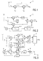
- Figure 1 shows a frequency-conversion circuit 1 that can be used in a telecommunication system 2 as schematically shown in figure 7.
- the telecommunication system can be a transmission system, such as a radio transmission system, a cordless or cellular telephone system or the like, an audio- or video system, a control system, a telemetry system, a local area network, a wide area network etcetera.
- Such a frequency-conversion circuit 1 can be used for frequency up conversion or frequency down conversion dependent on the application in a transmitter 4 or receiver 3, respectively.
- figures 1-3 relate to frequency-conversion circuits 1 used in a receiver 3, although the frequency-conversion circuits 1 could equally well be used in a transmitter 4 or transceiver 5.
- the frequency-conversion circuit 1 comprises an antenna 6 connected to a multistage frequency-converting means 7 showing two conversion stages or mixing stages 7-1 and 7-2 having oscillator inputs referred to in this figure as f L1 and f L2 .
- the multistage frequency-converting means 7 could include more than two stages although nowadays this is quite uncommon.
- the antenna signal f A is mixed in stage 7-1 with a first local oscillator signal f L1 and the resulting mixed signal is then mixed in stage 7-2 with a second local oscillator signal f L2 to reveal a baseband signal f B after demodulation (not shown in figures 1 and 2).
- f A f L1 + f L2 .
- the stage 7-1 shows in greater detail a quadrature down conversion in an 1-path and a Q-path.
- the I- and Q paths comprise a mixer 7-1I and 7-1Q, respectively, whereto I and Q local oscillator signals f L1 are applied from a frequency divider means 8-1 to be described hereafter.
- Appropriate 90° phase shifters are provided, as indicated, and the I and Q path signals are subtracted from each other in adder 9 to reveal an intermediate signal to be mixed in stage 7-2 with the second local oscillator signal f L2 provided by a frequency divider means 8-2, to be described hereafter, resulting in the baseband signal f B .
- a local oscillator 10 is coupled to inputs of the multistage frequency converting means 7-1 and 7-2, respectively, as shown in figure 3, that is to say connected through the series arrangement of both frequency divider means 8-1 and 8-2, or as shown in figure 2, connected through the parallel arrangement of both frequency divider means 8-1 and 8-2.
- FIG. 3 shows a detailed embodiment of how the frequency divider means 8-1, 8-2 are included in only one phase-locked loop 11.
- the phase-locked loop 11 further comprises the local oscillator in the form of a generally tunable voltage-controlled oscillator 10 having a control input 12 and an oscillator output 13 coupled to the frequency divider means 8-1, which is connected in series to the frequency divider means 8-2 and a further divider 14, which is connected to an input 15 of a phase discriminator 16.
- the phase discriminator 16 has a reference frequency input for inputting a reference signal f REF , such as a signal from a conventional crystal oscillator (not shown) and an output 17 coupled to the control input 12 of the voltage controlled oscillator 10 through a loop filter 18 for a stable control of the PLL.
- a reference signal f REF such as a signal from a conventional crystal oscillator (not shown)
- the further divider 14 has a divisor that, in dependence on the divisor of the frequency divider means, matches the local oscillator frequency to the frequency of f REF .
- the frequency divider means comprises counter means 8-1, 8-2. These counter means easily provide the 1 and Q oscillator signals for both f L1 and f L2 signals. Embodiments thereof will be presented in figures 4-6.
- Figure 3 further shows details of mixing stage 7-2, which is divided in a first pair of branches, which are connected to mixer 7-1I and which comprise mixers 7-2aI and 7-2aQ, which are connected with minus and plus signs to adders 19 and 20, respectively, and in a second pair of branches, connected to mixer 7-1Q and which comprise mixers 7-2bI and 7-2bQ, whixh are connected both with plus signs to the adders 19 and 20, respectively.
- Quadrature output signals of the adders 19 and 20 are led to a demodulator 21 through bandpass filters 22 and 23, respectively, revealing the actual baseband signal f B .
- these filters 22 and 23 can be embodied as low-pass filters.
- the counter means 8-1, 8-2 are simple binary counters which divide the input-signal frequency by 2.
- f A 900 MHz
- Tuning can be achieved by stepping of the local oscillator 10 at 4/3 times the channel spacing steps.
- the local oscillator frequency does not conincide with the RF-antenna frequency, also crosstalk problems are significantly reduced.
- an excellent image suppression is achieved in a way which is easy to integrate on a chip, and which does not require external components or, in the case of zero-IF, filters that are very difficult or impossible integrate, such as polyphase filters, multimixer filters, sequence asymmetric filters and the like.
- Figure 4 shows a simple way of connecting two 2-counters 8-1 and 8-2 that will generally be included in a phase-locked loop as shown in figure 3.
- Figure 5 shows an embodiment of counters 24 and 25 in a possible parallel arrangement Apart from devisors which are equal to 2, also divisors having a different value could be implemented, if necessary.
- An embodiment of a counter means, such as 8-2, embodied as a 3-counter is shown in figure 6, the 3-counter being built up from easy to integrate 2-counters 26 and 27 having reset inputs R jointly connected to an output 28 of a gate means formed as an AND-port 29.
- An output 30 of the counter 26, and an input 31 of the counter 27 are jointly connected to a first input 32 of the AND-port 29, whose second input 33 is connected to output 34 of the counter 27 for outputting a signal whose frequency is divided by 3 relative to the signal on input 35 of the counter 26.
Abstract
Description
- The present invention relates to a frequency-conversion circuit with a multistage frequency-converting means, to a telecommunications system, a receiver, a transmitter, a transceiver, an integrated circuit, and a telephone device provided with such a frequency-conversion circuit.
- Such a frequency-conversion circuit is known from "High Integration CMOS RF Transceivers", Proc. of the Workshop on Advances in Analog Circuit Design, April 2-3-4, 1996, Lausanne-Ouchy, Switzerland, by F. Brianti et al., 14 pages. This article describes in particular integrated digital radio architectures having a frequency up or down converting means usable, for example, in low-IF, such as zero-IF, or wideband-IF configurations. By definition, a low-IF configuration, such as a receiver, transmitter or transceiver, is a configuration, wherein the intermediate frequency (IF) is close to zero, or zero in case of a zero-IF. Some known advantages of zero-IF configurations are the high degree of integration on a chip that can be achieved as compared to a heterodyne or conventional IF configuration, because of the possibility to apply filters, such as low-pass filters for channel selectivity, than can be integrated at low cost. Reduced power dissipation, fewer interference problems and better crosstalk control than in a conventional configuration that requires external components can be achieved with a careful design of using this zero-IF architecture. The frequency conversion is implemented by means of two stages of mixers (see figure 2) resulting in a multistage frequency conversion in order to reduce the requirements imposed upon image rejection filters in front of the mixers as compared to conventional architectures. The mixer stages are quadrature mixers stages each having an I-path and a Q-path in order to properly distinguish between positive and negative frequencies, corresponding to upper and lower sidebands of an input RF signal. These quadrature mixers eliminate an off-chip IF filter function. Each of the two stages is being fed by a separate voltage-controlled oscillator (VCO) phase-locked loop (PLL) synthesizer circuit. Both synthesizer circuits are connected to a common crystal oscillator. The problem of the known frequency conversion circuit is that two synthesizer circuits are needed, which circuits lead to significant costs and require a large surface area and much power.
- JP-A-63175507 discloses a microwave frequency converting circuit which has two oscillator inputs both coupled to an oscillator output. A frequency multiplier is present between the oscillator output and one of the oscillator inputs. Such a sliding IF topology wherein both the local oscillator signals are sliding together (with a fixed frequency ratio) to perform the channel selection is well known.
- A two-stage frequency conversion circuit is also shown in DE-A-3 726 181.
- It is an object of the present invention to reduce the chip area and power consumption needed for the integrated architectures.
- A first aspect of the invention provides a frequency-conversion circuit with a multistage frequency converting means as claimed in claim 1. A second aspect of the invention provides a receiver as claimed in
claim 3. A third aspect of the invention provides a transmitter as claimed in claim 5 A fourth aspect of the invention provides a telecommunications system as claimed in claim 6. A fifth aspect of the invention provides a transceiver as claimed inclaim 7. A sixth aspect of the invention provides an integrated circuit as claimed in claim 8. A seventh aspect of the invention provides a telephone device as claimed in claim 9. Advantageous embodiments are defined in the dependent claims. - In an embodiment of the frequency-conversion circuit according to the invention, the frequency divider means comprises a counter means. Such counter means are very simple to integrate. Furthermore, the counter means provide for an exact relation as a function in time, in particular the phase, between the respective oscillator signals intended for each stage of the multistage frequency-converting means. Because of the inherent phase accuracy between the respective oscillator signals derived from both respective outputs of the counter means, a good image or mirror signal suppression is automatically achieved so that, if necessary at all, a modest image rejection-suppression filter will be sufficient in practice to reveal a high-quality frequency conversion. In general, the counter means already have or can easily be provided with outputs for providing both the I and Q oscillator signals to be applied to the I an Q paths respectively, of the multistage frequency-converting means. So separate 90° phase shifters are no longer necessary in the coupling or direct connection between the generally local oscillator and, in particular, the Q paths' oscillator inputs of the multistage frequency-converting means.
- These and other aspects and advantages of the present invention will be apparent from and further elucidated with reference to the embodiments and figures described hereinafter. Similar elements in the separate figures are provided with the same reference numerals. In the drawing:
- Fig. 1 shows a principle scheme of one embodiment of the frequency-conversion circuit according to the present invention;
- Fig. 2 shows an elaborate worked out embodiment of one stage of a multistage frequency-converting means, and a second stage thereof for application in the frequency-conversion circuit of figure 1;
- Fig. 3 shows another embodiment of the frequency-conversion circuit according to the invention;
- Fig. 4 shows a frequency divider means comprising a series arrangement of counters for application in the frequency-conversion circuit according to the invention;
- Fig. 5 shows a frequency divider means comprising a parallel arrangement of counters for application in the frequency-conversion circuit according to the invention;
- Fig. 6 shows a frequency divided by 3 means for application in the frequency divider means of figures 4 or 5; and
- Fig. 7 schematically shows a telecommunication system comprising transmitters and/or receivers having one or more frequency-conversion circuits according to the invention.
- Figure 1 shows a frequency-conversion circuit 1 that can be used in a
telecommunication system 2 as schematically shown in figure 7. Thetelecommunication system 2 shown comprises one ormore receivers 3,transmitters 4, and/or transceivers (=transmitter/receiver) 5, each of which contains apart from other circuits, the frequency-conversion circuit 1. The telecommunication system can be a transmission system, such as a radio transmission system, a cordless or cellular telephone system or the like, an audio- or video system, a control system, a telemetry system, a local area network, a wide area network etcetera. Such a frequency-conversion circuit 1 can be used for frequency up conversion or frequency down conversion dependent on the application in atransmitter 4 orreceiver 3, respectively. - For the sake of simplification of the description, figures 1-3 relate to frequency-conversion circuits 1 used in a
receiver 3, although the frequency-conversion circuits 1 could equally well be used in atransmitter 4 ortransceiver 5. - The frequency-conversion circuit 1 comprises an antenna 6 connected to a multistage frequency-converting means 7 showing two conversion stages or mixing stages 7-1 and 7-2 having oscillator inputs referred to in this figure as fL1 and fL2. The multistage frequency-converting means 7 could include more than two stages although nowadays this is quite uncommon. The antenna signal fA is mixed in stage 7-1 with a first local oscillator signal fL1 and the resulting mixed signal is then mixed in stage 7-2 with a second local oscillator signal fL2 to reveal a baseband signal fB after demodulation (not shown in figures 1 and 2). For zero-IF fA = fL1 + fL2.
- In figure 2, the stage 7-1 shows in greater detail a quadrature down conversion in an 1-path and a Q-path. The I- and Q paths comprise a mixer 7-1I and 7-1Q, respectively, whereto I and Q local oscillator signals fL1 are applied from a frequency divider means 8-1 to be described hereafter. Appropriate 90° phase shifters are provided, as indicated, and the I and Q path signals are subtracted from each other in adder 9 to reveal an intermediate signal to be mixed in stage 7-2 with the second local oscillator signal fL2 provided by a frequency divider means 8-2, to be described hereafter, resulting in the baseband signal fB. A
local oscillator 10 is coupled to inputs of the multistage frequency converting means 7-1 and 7-2, respectively, as shown in figure 3, that is to say connected through the series arrangement of both frequency divider means 8-1 and 8-2, or as shown in figure 2, connected through the parallel arrangement of both frequency divider means 8-1 and 8-2. - Figure 3 shows a detailed embodiment of how the frequency divider means 8-1, 8-2 are included in only one phase-locked
loop 11. The phase-lockedloop 11 further comprises the local oscillator in the form of a generally tunable voltage-controlledoscillator 10 having acontrol input 12 and anoscillator output 13 coupled to the frequency divider means 8-1, which is connected in series to the frequency divider means 8-2 and afurther divider 14, which is connected to aninput 15 of aphase discriminator 16. Thephase discriminator 16 has a reference frequency input for inputting a reference signal fREF, such as a signal from a conventional crystal oscillator (not shown) and anoutput 17 coupled to thecontrol input 12 of the voltage controlledoscillator 10 through aloop filter 18 for a stable control of the PLL. Thefurther divider 14 has a divisor that, in dependence on the divisor of the frequency divider means, matches the local oscillator frequency to the frequency of fREF. In the case shown here, the frequency divider means comprises counter means 8-1, 8-2. These counter means easily provide the 1 and Q oscillator signals for both fL1 and fL2 signals. Embodiments thereof will be presented in figures 4-6. - Figure 3 further shows details of mixing stage 7-2, which is divided in a first pair of branches, which are connected to mixer 7-1I and which comprise mixers 7-2aI and 7-2aQ, which are connected with minus and plus signs to
adders adders adders demodulator 21 throughbandpass filters filters - The operation of the frequency- conversion circuit 1 of figure 3 will now be described for the case wherein the counter means 8-1, 8-2 are simple binary counters which divide the input-signal frequency by 2. Assuming fA=900 MHz, a local oscillator frequency of 1200 MHz, will lead to a value of fL1=1200/2=600 MHz. Consequently, fL2=600/2=300 MHz and the output signal after the second stage 7-2 will lie in the baseband. Tuning can be achieved by stepping of the
local oscillator 10 at 4/3 times the channel spacing steps. Moreover, because in this example the local oscillator frequency does not conincide with the RF-antenna frequency, also crosstalk problems are significantly reduced. In addition, an excellent image suppression is achieved in a way which is easy to integrate on a chip, and which does not require external components or, in the case of zero-IF, filters that are very difficult or impossible integrate, such as polyphase filters, multimixer filters, sequence asymmetric filters and the like. - If, in general, in the series arrangement of counters, the first counter means 8-1 has divisor i and the second counter means 8-2 has divisor j, than the equation for zero-IF is:

- Figure 4 shows a simple way of connecting two 2-counters 8-1 and 8-2 that will generally be included in a phase-locked loop as shown in figure 3. By vurtue thereof, an easily integratable fixed phase relation between the I- and Q-outputs is achieved, which reduces problems that emanate from a varying phase. Figure 5 shows an embodiment of
counters output 28 of a gate means formed as an AND-port 29. Anoutput 30 of the counter 26, and aninput 31 of the counter 27 are jointly connected to afirst input 32 of the AND-port 29, whosesecond input 33 is connected to output 34 of the counter 27 for outputting a signal whose frequency is divided by 3 relative to the signal oninput 35 of the counter 26.
Claims (9)
- A frequency-conversion circuit with a multistage frequency converting means comprising:a tunable voltage-controlled oscillator (10) having an oscillator output (13) for supplying an oscillator signal,a first quadrature mixing stage having an I and a Q path and comprising a first mixer (7-1I) and a second mixer (7-1Q) for receiving a first local oscillator signal (fL1), anda second quadrature mixing stage having an I and an Q path and comprising a third mixer (7-2aI), a fourth mixer (7-2aQ), a fifth mixer (7-2bI), and a sixth mixer (7-2bQ) for receiving a second local oscillator signal (fL2), whereinthe first mixer (7-1I) has a first input for receiving an I-component of the first local oscillator signal (fL1), a second input for receiving an antenna signal (fA), and an output for supplying a first output signal,the second mixer (7-1Q) has a first input for receiving a Q-component of the first local oscillator signal (fL1), a second input for receiving the antenna signal (fA), and an output for supplying a second output signal,the third mixer (7-2aI) has a first input for receiving an I-component of the second local oscillator signal (fL2), a second input for receiving the first output signal and an output connected to an inverting input of a first adder (19),the fourth mixer (7-2aQ) has a first input for receiving a Q-component of the second local oscillator signal (fL2), a second input for receiving the first output signal and an output connected to a non-inverting input of a second adder (20),the fifth mixer (7-2bI) has a first input for receiving an I-component of the second local oscillator signal (fL2), a second input for receiving the second output signal and an output connected to an non-inverting input of the second adder (20), andthe sixth mixer (7-2bQ) has a first input for receiving a Q-component of the second local oscillator signal (fL2), a second input for receiving the second output signal and an output connected to a non-inverting input of the first adder (19),characterized in that the multistage frequency converting means further comprises:a first frequency divider means (8-1) for receiving the oscillator signal to supply the first local oscillator signal (fL1), anda second frequency divider means (8-2) for receiving the oscillator signal or the first local oscillator signal (fL1) to supply the second local oscillator signal (fL2).
- A frequency-conversion circuit as claimed in claim 1, wherein the second frequency divider means (8-2) is arranged for receiving the first local oscillator signal (fL1) and wherein a relation between a frequency fLO of the oscillator signal and a divisor j of the first frequency divider means (8-1) and a divisor i of the second frequency divider means (8-2) is determined by:

wherein fA is a frequency of an antenna signal supplied to the first quadrature mixing stage. - A frequency-conversion circuit as claimed in claim 1, wherein the first frequency divider means (8-1) comprises a first counter and the second frequency divider means (8-2) comprises a second counter.
- A receiver comprising the frequency-conversion circuit as claimed in claim 1.
- A transmitter comprising the frequency-conversion circuit as claimed in claim 1.
- A telecommunications system comprising the frequency-conversion circuit as claimed in claim 1, the telecommunications system being one out of the group: a transmission system, a radio transmission system, a cordless or cellular telephone system, an audio or video system, a control system, a telemetry system, a local area network, or a wide area network.
- A transceiver comprising the frequency-conversion circuit as claimed in claim 1.
- An integrated circuit comprising the frequency-conversion circuit as claimed in claim 1.
- A telephone device comprising the frequency-conversion circuit as claimed in claim 1.
Priority Applications (1)
| Application Number | Priority Date | Filing Date | Title |
|---|---|---|---|
| EP98903224A EP0900481B1 (en) | 1997-03-12 | 1998-02-27 | A frequency conversion circuit |
Applications Claiming Priority (4)
| Application Number | Priority Date | Filing Date | Title |
|---|---|---|---|
| EP97200739 | 1997-03-12 | ||
| EP97200739 | 1997-03-12 | ||
| PCT/IB1998/000238 WO1998040968A2 (en) | 1997-03-12 | 1998-02-27 | A frequency conversion circuit |
| EP98903224A EP0900481B1 (en) | 1997-03-12 | 1998-02-27 | A frequency conversion circuit |
Publications (2)
| Publication Number | Publication Date |
|---|---|
| EP0900481A2 EP0900481A2 (en) | 1999-03-10 |
| EP0900481B1 true EP0900481B1 (en) | 2006-06-14 |
Family
ID=26146238
Family Applications (1)
| Application Number | Title | Priority Date | Filing Date |
|---|---|---|---|
| EP98903224A Expired - Lifetime EP0900481B1 (en) | 1997-03-12 | 1998-02-27 | A frequency conversion circuit |
Country Status (2)
| Country | Link |
|---|---|
| EP (1) | EP0900481B1 (en) |
| WO (1) | WO1998040968A2 (en) |
Families Citing this family (26)
| Publication number | Priority date | Publication date | Assignee | Title |
|---|---|---|---|---|
| US6061551A (en) | 1998-10-21 | 2000-05-09 | Parkervision, Inc. | Method and system for down-converting electromagnetic signals |
| US6694128B1 (en) | 1998-08-18 | 2004-02-17 | Parkervision, Inc. | Frequency synthesizer using universal frequency translation technology |
| US7515896B1 (en) | 1998-10-21 | 2009-04-07 | Parkervision, Inc. | Method and system for down-converting an electromagnetic signal, and transforms for same, and aperture relationships |
| US6560301B1 (en) | 1998-10-21 | 2003-05-06 | Parkervision, Inc. | Integrated frequency translation and selectivity with a variety of filter embodiments |
| US7039372B1 (en) | 1998-10-21 | 2006-05-02 | Parkervision, Inc. | Method and system for frequency up-conversion with modulation embodiments |
| US6370371B1 (en) | 1998-10-21 | 2002-04-09 | Parkervision, Inc. | Applications of universal frequency translation |
| US7236754B2 (en) | 1999-08-23 | 2007-06-26 | Parkervision, Inc. | Method and system for frequency up-conversion |
| US6813485B2 (en) | 1998-10-21 | 2004-11-02 | Parkervision, Inc. | Method and system for down-converting and up-converting an electromagnetic signal, and transforms for same |
| US6061555A (en) | 1998-10-21 | 2000-05-09 | Parkervision, Inc. | Method and system for ensuring reception of a communications signal |
| US6853690B1 (en) | 1999-04-16 | 2005-02-08 | Parkervision, Inc. | Method, system and apparatus for balanced frequency up-conversion of a baseband signal and 4-phase receiver and transceiver embodiments |
| US6879817B1 (en) | 1999-04-16 | 2005-04-12 | Parkervision, Inc. | DC offset, re-radiation, and I/Q solutions using universal frequency translation technology |
| US7693230B2 (en) | 1999-04-16 | 2010-04-06 | Parkervision, Inc. | Apparatus and method of differential IQ frequency up-conversion |
| US7110444B1 (en) | 1999-08-04 | 2006-09-19 | Parkervision, Inc. | Wireless local area network (WLAN) using universal frequency translation technology including multi-phase embodiments and circuit implementations |
| US7065162B1 (en) | 1999-04-16 | 2006-06-20 | Parkervision, Inc. | Method and system for down-converting an electromagnetic signal, and transforms for same |
| EP1517436B1 (en) * | 1999-10-07 | 2016-05-04 | Parkervision, Inc. | Down converter using subsampling |
| AU7863000A (en) * | 1999-10-07 | 2001-05-10 | Parkervision, Inc. | Dc offset, re-radiation, and i/q solutions using universal frequency translationtechnology |
| US6671332B1 (en) * | 1999-10-08 | 2003-12-30 | Medtronic, Inc. | Zero IF receiver with reduced AM detector |
| WO2001039364A1 (en) * | 1999-11-22 | 2001-05-31 | Parthus Technologies Plc. | Two stage quatrature down converter for gps and glonass |
| US6634555B1 (en) | 2000-01-24 | 2003-10-21 | Parker Vision, Inc. | Bar code scanner using universal frequency translation technology for up-conversion and down-conversion |
| US7010286B2 (en) | 2000-04-14 | 2006-03-07 | Parkervision, Inc. | Apparatus, system, and method for down-converting and up-converting electromagnetic signals |
| US7454453B2 (en) | 2000-11-14 | 2008-11-18 | Parkervision, Inc. | Methods, systems, and computer program products for parallel correlation and applications thereof |
| US7072427B2 (en) | 2001-11-09 | 2006-07-04 | Parkervision, Inc. | Method and apparatus for reducing DC offsets in a communication system |
| US7460584B2 (en) | 2002-07-18 | 2008-12-02 | Parkervision, Inc. | Networking methods and systems |
| US7379883B2 (en) | 2002-07-18 | 2008-05-27 | Parkervision, Inc. | Networking methods and systems |
| US8346091B2 (en) | 2009-04-29 | 2013-01-01 | Andrew Llc | Distributed antenna system for wireless network systems |
| EP2915301B1 (en) | 2012-10-31 | 2017-09-20 | CommScope Technologies LLC | Digital baseband transport in telecommunications distribution systems |
Citations (1)
| Publication number | Priority date | Publication date | Assignee | Title |
|---|---|---|---|---|
| JPS63175507A (en) * | 1987-01-14 | 1988-07-19 | Toshiba Corp | Microwave frequency converting circuit |
Family Cites Families (1)
| Publication number | Priority date | Publication date | Assignee | Title |
|---|---|---|---|---|
| CH671856A5 (en) * | 1986-09-05 | 1989-09-29 | Ascom Radiocom Ag |
-
1998
- 1998-02-27 WO PCT/IB1998/000238 patent/WO1998040968A2/en active IP Right Grant
- 1998-02-27 EP EP98903224A patent/EP0900481B1/en not_active Expired - Lifetime
Patent Citations (1)
| Publication number | Priority date | Publication date | Assignee | Title |
|---|---|---|---|---|
| JPS63175507A (en) * | 1987-01-14 | 1988-07-19 | Toshiba Corp | Microwave frequency converting circuit |
Also Published As
| Publication number | Publication date |
|---|---|
| EP0900481A2 (en) | 1999-03-10 |
| WO1998040968A3 (en) | 1999-02-18 |
| WO1998040968A2 (en) | 1998-09-17 |
Similar Documents
| Publication | Publication Date | Title |
|---|---|---|
| US6282413B1 (en) | Multistaged frequency conversion with single local oscillator | |
| EP0900481B1 (en) | A frequency conversion circuit | |
| US6731923B2 (en) | Direct conversion circuit for radio frequency signals | |
| EP0800283B1 (en) | Transmitter/receiver for transmitting and receiving of an RF signal in two frequency bands | |
| US7715802B2 (en) | Frequency synthesizer and multi-band radio apparatus using said frequency synthesizer | |
| US6766178B1 (en) | RF architecture for cellular multi-band telephones | |
| EP1219019B1 (en) | Local oscillator apparatus for radio frequency communication systems | |
| US7327993B2 (en) | Low leakage local oscillator system | |
| US6085075A (en) | Communication system, a communication device and a frequency synthesizer | |
| EP0968570A1 (en) | A multi-carrier radio system and radio transceiver implementation | |
| WO1998052292A1 (en) | Dual-band radio receiver | |
| US5819161A (en) | Two way radio set utilizing a single oscillator | |
| US6785518B2 (en) | Transmitter and receiver circuit for radio frequency signals | |
| KR19990078108A (en) | Dual band mobile phone handset | |
| RU2348104C2 (en) | Frequency synthesiser for support of voice communication standards and wireless networks standards | |
| US7356324B2 (en) | Mobile radio receiver device | |
| US7277623B2 (en) | Equal duty cycle frequency divider | |
| US6741865B1 (en) | Digital multi-subscriber radio telecommunication system working with frequency jumping | |
| WO2001071934A1 (en) | Communication system with frequency modulation and with a single local oscillator | |
| US20090098833A1 (en) | Optical module | |
| KR20000026298A (en) | Converter for lowering multi-phase low frequency to use cmos radio communication transceiver and method the same | |
| EP1748560A1 (en) | Frequency divider for generating an output signal having fifty percent duty cycle |
Legal Events
| Date | Code | Title | Description |
|---|---|---|---|
| PUAI | Public reference made under article 153(3) epc to a published international application that has entered the european phase |
Free format text: ORIGINAL CODE: 0009012 |
|
| AK | Designated contracting states |
Kind code of ref document: A2 Designated state(s): DE FR GB |
|
| 17P | Request for examination filed |
Effective date: 19981214 |
|
| 17Q | First examination report despatched |
Effective date: 20030312 |
|
| GRAP | Despatch of communication of intention to grant a patent |
Free format text: ORIGINAL CODE: EPIDOSNIGR1 |
|
| GRAS | Grant fee paid |
Free format text: ORIGINAL CODE: EPIDOSNIGR3 |
|
| GRAA | (expected) grant |
Free format text: ORIGINAL CODE: 0009210 |
|
| AK | Designated contracting states |
Kind code of ref document: B1 Designated state(s): DE FR GB |
|
| REG | Reference to a national code |
Ref country code: GB Ref legal event code: FG4D |
|
| REF | Corresponds to: |
Ref document number: 69834875 Country of ref document: DE Date of ref document: 20060727 Kind code of ref document: P |
|
| REG | Reference to a national code |
Ref country code: GB Ref legal event code: 732E |
|
| ET | Fr: translation filed | ||
| PLBE | No opposition filed within time limit |
Free format text: ORIGINAL CODE: 0009261 |
|
| REG | Reference to a national code |
Ref country code: FR Ref legal event code: TP |
|
| STAA | Information on the status of an ep patent application or granted ep patent |
Free format text: STATUS: NO OPPOSITION FILED WITHIN TIME LIMIT |
|
| 26N | No opposition filed |
Effective date: 20070315 |
|
| PGFP | Annual fee paid to national office [announced via postgrant information from national office to epo] |
Ref country code: FR Payment date: 20120316 Year of fee payment: 15 |
|
| REG | Reference to a national code |
Ref country code: FR Ref legal event code: ST Effective date: 20131031 |
|
| PG25 | Lapsed in a contracting state [announced via postgrant information from national office to epo] |
Ref country code: FR Free format text: LAPSE BECAUSE OF NON-PAYMENT OF DUE FEES Effective date: 20130228 |
|
| PGFP | Annual fee paid to national office [announced via postgrant information from national office to epo] |
Ref country code: GB Payment date: 20140127 Year of fee payment: 17 |
|
| GBPC | Gb: european patent ceased through non-payment of renewal fee |
Effective date: 20150227 |
|
| PG25 | Lapsed in a contracting state [announced via postgrant information from national office to epo] |
Ref country code: GB Free format text: LAPSE BECAUSE OF NON-PAYMENT OF DUE FEES Effective date: 20150227 |
|
| PGFP | Annual fee paid to national office [announced via postgrant information from national office to epo] |
Ref country code: DE Payment date: 20170119 Year of fee payment: 20 |
|
| REG | Reference to a national code |
Ref country code: DE Ref legal event code: R071 Ref document number: 69834875 Country of ref document: DE |