EP0903882B1 - Stable wavelength division multiplex ring network - Google Patents
Stable wavelength division multiplex ring network Download PDFInfo
- Publication number
- EP0903882B1 EP0903882B1 EP98307235.6A EP98307235A EP0903882B1 EP 0903882 B1 EP0903882 B1 EP 0903882B1 EP 98307235 A EP98307235 A EP 98307235A EP 0903882 B1 EP0903882 B1 EP 0903882B1
- Authority
- EP
- European Patent Office
- Prior art keywords
- network
- wavelength
- ring network
- wavelength division
- division multiplexed
- Prior art date
- Legal status (The legal status is an assumption and is not a legal conclusion. Google has not performed a legal analysis and makes no representation as to the accuracy of the status listed.)
- Expired - Lifetime
Links
Images


Classifications
-
- H—ELECTRICITY
- H04—ELECTRIC COMMUNICATION TECHNIQUE
- H04J—MULTIPLEX COMMUNICATION
- H04J14/00—Optical multiplex systems
- H04J14/02—Wavelength-division multiplex systems
- H04J14/0287—Protection in WDM systems
- H04J14/0289—Optical multiplex section protection
- H04J14/0291—Shared protection at the optical multiplex section (1:1, n:m)
-
- H—ELECTRICITY
- H04—ELECTRIC COMMUNICATION TECHNIQUE
- H04J—MULTIPLEX COMMUNICATION
- H04J14/00—Optical multiplex systems
- H04J14/02—Wavelength-division multiplex systems
- H04J14/0221—Power control, e.g. to keep the total optical power constant
-
- H—ELECTRICITY
- H04—ELECTRIC COMMUNICATION TECHNIQUE
- H04J—MULTIPLEX COMMUNICATION
- H04J14/00—Optical multiplex systems
- H04J14/02—Wavelength-division multiplex systems
- H04J14/0227—Operation, administration, maintenance or provisioning [OAMP] of WDM networks, e.g. media access, routing or wavelength allocation
- H04J14/0241—Wavelength allocation for communications one-to-one, e.g. unicasting wavelengths
-
- H—ELECTRICITY
- H04—ELECTRIC COMMUNICATION TECHNIQUE
- H04J—MULTIPLEX COMMUNICATION
- H04J14/00—Optical multiplex systems
- H04J14/02—Wavelength-division multiplex systems
- H04J14/0278—WDM optical network architectures
- H04J14/0283—WDM ring architectures
-
- H—ELECTRICITY
- H04—ELECTRIC COMMUNICATION TECHNIQUE
- H04J—MULTIPLEX COMMUNICATION
- H04J14/00—Optical multiplex systems
- H04J14/02—Wavelength-division multiplex systems
- H04J14/0201—Add-and-drop multiplexing
-
- H—ELECTRICITY
- H04—ELECTRIC COMMUNICATION TECHNIQUE
- H04J—MULTIPLEX COMMUNICATION
- H04J14/00—Optical multiplex systems
- H04J14/02—Wavelength-division multiplex systems
- H04J14/0227—Operation, administration, maintenance or provisioning [OAMP] of WDM networks, e.g. media access, routing or wavelength allocation
Landscapes
- Engineering & Computer Science (AREA)
- Computer Networks & Wireless Communication (AREA)
- Signal Processing (AREA)
- Optical Communication System (AREA)
- Small-Scale Networks (AREA)
- Lasers (AREA)
Description
- This invention relates to Wavelength Division Multiplex (WDM) ring network and, more particularly, to the prevention of lasing in such WDM ring networks .
- The growth and diversity of lightwave networks, such as Wavelength Division Multiplexed (WDM) networks are placing new demands on capacity management and provisioning, maintenance, and reliable and robust operation. One type of WDM network is a WDM ring network which may, for example, be used for metropolitan area network applications. The reliability problem in WDM ring networks is particularly significant since the use of closed cyclical paths makes lasing possible if the roundtrip optical gain exceeds the loop loss. The lasing affects signal channels through cross saturation and causes power variations which may reduce system power margins and cause false alarms in system channel monitoring.
- A typical WDM optical ring network includes network elements with Wavelength Add/Drop (WAD) capability, whereby some optical channels are dropped and/or added while other channels are expressed, i.e., passed through. Depending on the technology used for WAD elements and the network architecture, closed loops may be formed in the WDM ring network which, with the Erbium-Doped Fiber Amplifiers (EDFA's) used to compensate the losses of network elements and fibers, can constitute ring laser cavities. Laser oscillations in the ring cavity, occurring if the round trip gain experienced by Amplified Spontaneous Emissions (ASE) exceeds the loop loss, may increase amplifier saturation and introduce additional noise, which affect the performance of optical signal transmission. Such effects have been reported by K. Bala and C. A. Brackett, J. Lightwave Tech., 14(1585), 1996 and by J. Iness, et al, J. Lightwave Tech., 14(1207), 1996.
- Overcoming the undesirable lasing in ring networks has not been particularly addressed in the art - as its focus has remained elsewhere. More particularly, A.F.Elrefaie, in an article entitled "Multiwavelength Survivable Ring Network Architectures", which appeared in PROCEEDINGS OF THE INTERNATIONAL CONFERENCE ON COMMUNICATIONS (ICC) Geneva, May 23-26, 1993, New York, IEEE, US, vol. 3, 23 May 1993, pp.1245-1251; generally discloses a new architecture for implementing unidirectional and bidirectional self-healing interoffice ring networks using WDM technology. The working rings disclosed therein use all-optical drop-and-add multiplexers at each office and any protection paths use optical amplifiers and optical switches.
- United States Patent No.
5,510,926 issued to Bayart et al on April 23, 1996 describes a transmission method using spectrum multiplexing with amplification, in which method data to be transmitted is carried by various carrier waves occupying respective optical spectrum channels, it being possible for the number and/or the power of the carrier waves to vary, the various carrier waves being amplified by a common amplifier having respective gains for the various channels, while having limited overall amplifying power, wherein provision is made to make all of the gains equal in the presence of a fixed number of fixed-power carrier waves, regulation light that is independent of the carrier waves and that is amplified by the amplifier being servo-controlled in power so as to maintain equality between the gains in the presence of variations in the number and/or power of the carrier waves. - In another article authored by John L. Zyskind et al entitled "Fast Link Control Protection for Surviving Channels In Multiwavelength Optical Networks", which appeared at ECOC'96, vol.5, 15 September 1996, pp, 49-52, OSLO, link control, a technique for protecting surviving channels on a perlink basis from fast power transients resulting from network reconfigurations or line failures is described as applied to a 560-km eight-amplifier wavelength division multiplexed link carrying seven 2.5-Gb/s channels plus the link control channel.
- In European Patent
EP0647994 (AT&T Corp., 12-APR-1995) a potentially inexpensive light for multi-channel wavelength-division-multiplexed (WDM) applications was described. The high-power amplified spontaneous emission (ASE) from a fiber amplifier, which is already in an optical fiber, is efficiently divided into many channels using a WDM demultiplexer. This "spectrum-sliced" ASE is used as light sources for WDM systems rather than several wavelength-selected DFB lasers. - European Patent
EP0695050 (PIRELLI CAVI SPA, 31-JAN-1996) describes an optical telecommunications system comprising a means for generating optical signals of different wavelengths, an optical-fiber line with amplifier, a pre-amplifier and receiver wherein the pre-amplfier comprises optical waveguide doped with a rare earth material, differential-attenuator located at a first position along the doped waveguide which causes an attenuation in the signal band which is greater than the attenuation caused at the pumping wavelength, and filter located at a second position and adapted to attenuate by a value higher than a predetermined minimum, the spontaneous emission in a wavelength band contiguous with the signal band. The position and attenuation of the differential-attenuator and filter and wavelength band are selected in a functional relation with respect to each other in order to limit the output power variations from the pre-amplifier. - Finally, patent
WO 96/32787 A - The network provides protective switching of traffic and solves the problem of circulating ASE in a simple and economical way. Finally the network also permits wavelength reconfiguration to reduce the number of required wavelengths.
- Despite these developments, what is needed is a technique for preventing these WDM ring networks from lasing.
- We have recognized that in a Wavelength Division Multiplex (WDM) ring network with a closed loop, the possibility of lasing at Amplified Spontaneous Emissions (ASE) wavelengths exists. We have determined that depending on the structure and operating condition, cross saturation caused by laser may be a problem. In the worst case, the problem can be so severe that the power of some signal channels be greatly reduced, which will reduce system power margins and cause false alarms, when channel loading in part of the ring is changed even though there is no fault in the ring.
- We provide a technique for protecting against lasing in a WDM ring network comprising a plurality of serially connected node links, each node link including a segment of optical fiber and an access node site for adding or dropping one or more active wavelength channels to a transmission bandwidth of the network. In accordance with the present invention, protection means, connected to the network, changes the optical transmission characteristics of the network to ensure that the network loop gain at any wavelength is always less than the network loop loss.
- In one embodiment the protection means changes the optical transmission characteristics of an inactive portion of the transmission bandwidth of the network to ensure that the loop gain at that inactive portion is less than the loop loss. In another embodiment, the protection means includes pump and link control. The protection means utilizes access node control algorithms.
- In the drawings,
-
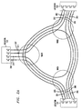
Fig. 1 shows a schematic of an illustrative WDM ring network useful in describing the operation of the present invention; -
Figs. 2a and2b show a simplified diagram of the WDM ring network ofFIG. 1 which shows the signal channels which are added and dropped at each WAD location, where each line represent 4 signal channels and the dashed line represents 2 channels; -
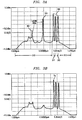
Fig. 3 (a) illustrates the spectrum ofFig. 2(a) where lasing appears at two wavelengths to the left of the three signal wavelengths when the WDM ring network inFig. 1 is closed; andFig. 3(b) shows that lasing is suppressed when each of the attenuators in the three WAD sites are increased by 1 dB; andFig. 3(c) shows that lasing happens when λa added to WAD1 is cut, as compared to the normal operation shown inFig 3(b) ; -
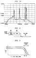
Fig. 4 illustrates a typical block diagram of a typical EDFA; -
Fig. 5 illustrates an illustrative plot of gain versus input power for a typical EDFA ofFig. 4 ; -
Fig. 6 illustrates a typical diagram of a Dragone router for use in a WAD site; and -
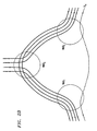
Fig. 7 shows how the techniques of the present invention may be utilized in an illustrative double WDM ring network. - With reference to
Fig 1 , there is shown a schematic of an illustrative WDM ring network, e.g., a metropolitan area network, including three access nodes or sites (e.g., Wavelength Add/Drop (WAD) sites,WAD1- WAD3),101-103, interspersed by three optical fiber spans 104 - 106. Each node link, e.g., 101/104 - 103/106, includes an access site, e.g.,WAD1 - WAD3, and an optical fiber segment, e.g.,104 - 106, respectively. Each of the WAD1 - WAD3 sites, 101 - 103, is shown to include a WAD element, respectively, 107 - 109, and an optical amplifier, respectively, 111 - 113. Each of the WAD elements 107 - 109 are, illustratively, shown to include fiber gratings and circulators. - Illustratively, the optical amplifiers 111 - 113 are Erbium-Doped Fiber Amplifiers (EDFAs) which provide optical gain to compensate for the loss in the prior corresponding node link (defined herein as a node and an optical fiber segment). Thus, for example amplifier 111 would be arranged to compensate for the loss in
optical fiber span 104, and the gratings, couplers and fiber connectors of itsWAD element 107. In a typical installation each of the node links, e.g., 101/104 - 103/106 are arranged to have the gain of the amplifier cancel the loss of the fiber and WAD element in its link. As a result, when the node links 101/104 - 103/106 are serially connected end-to-end into a WDM ring network, if the gain spectrum is flat, the overall loop gain would be zero for any signal wavelength which traverses the WDM ring network. Since in all WDM ring networks no signal wavelength traverses the entire ring network (otherwise the signal wavelength would exit at the same node from which it originated), providing a zero loop gain requirement would appear to be sufficient to prevent lasing in the WDM ring network. We have recognized that while a zero loop gain provides stable operations at the signal wavelengths, it may not prevent lasing at Amplified Stimulated Emissions (ASE) wavelengths of a typical EDFA. Such lasing may severely degrade the performance of the WDM ring network. - With continued reference to
Fig. 1 , in one particular illustrative WDM network the three WAD sites, WAD1, WAD2, and WAD3, are connected by three spans 104-106 of optical fibers of lengths L1 = 15.94, L 2 = 14.49, and L 3 = 11.13 km, respectively. With joint reference toFig. 1 and2a , we also assume that sixteen WDM signal channels are propagated clockwise in the ring. Eight signal channels exist between WAD1 and WAD2, including 8 channels originating (201 ofFig. 2a ) at location121 of WAD1 and terminating (202 ofFig. 2a ) atlocation 122 of WAD2 and 8 channels originating (203 ofFig. 2a ) at location122 of WAD2 and terminating (204 ofFig. 2a ) atlocation 121 of WAD1. As shown each path inFig. 2(a) represents 4 channels. Four channels exist between WAD2 and WAD3, including 4 channels originating (205 ofFig. 2a ) at location121 of WAD1 and terminating (206 ofFig. 2a ) atlocation 123 of WAD3 and 4 channels originating (207 ofFig. 2a ) at location123 of WAD3 and terminating (208 ofFig. 2a ) atlocation 121 of WAD1. Four channels also exist between WAD2 and WAD3, including 4 channels originating (209 ofFig. 2a ) at location122 of WAD2 and terminating (210 ofFig. 2a ) atlocation 123 of WAD3 and 4 channels originating (211 ofFig. 2a ) at location123 of WAD3 and terminating (212 ofFig. 2a ) atlocation 122 of WAD2. For illustrative purposes, the three groups of channels were represented with 3 lasers at the wavelengths of λa = 1552.4 um, λb = 1554.0 um, and λc = 1556.1 um, respectively. - With reference to
Fig. 1 , at each WAD sites 101 - 103, all the received signal channels are amplified with an Erbium-Doped Fiber Amplifiers (EDFA) 111 - 113, respectively, before they either passed through or were dropped. In the following description the symbol λa b indicates a wavelength, where the subscript denotes the wavelength, e.g., b, and the superscript denotes whether that wavelength has been added "a" or dropped "d". For example, at WAD1 two gratings 161 and 162 at the added wavelengths λa a , λa b and twogratings circulators circulator 152 fromlocation 121 and are reflected by the gratings 161 and 162, respectively, and exit the output port ofcirculator 152 tooptical fiber span 104. - In a similar manner, between the two
circulators 153 and 154 of WAD2 are inserted two gratings to add the wavelengths λa a, λa c and two gratings to drop the wavelengths λd a, λd c. Similarly, between the twocirculators - In a typical WDM ring network, where each of the signal channels are at a different wavelength, there would be a separate grating for each of the different wavelengths being added and a separate grating for each of the different wavelengths being dropped. Thus for our example, WAD1 would have 12 gratings for the 12 added wavelengths (8 from the group λa a and 4 from the group λa b) and 12 grating for the 12 dropped wavelengths (8 from group λd a and 4 from group λd b). Similarly, the total at WAD2 would also include 12 grating for the 12 added wavelengths (λa a, λa c) and 12 grating for the 12 dropped wavelengths (λd a, λd c). The total at WAD3 would include 8 grating for the 8 added wavelengths (λa c, λa b) and 8 grating for the 8 dropped wavelengths (λd b, λd c). However it should be noted, with reference to WAD1, that if the same wavelength, e.g., λa, is to be dropped and then added at WAD1 (which is typical in an add/drop circuit), then one of the grating 162 or 164 can be eliminated since only one grating is needed at that dropped/added wavelength λa.
- The WAD elements may be implemented using the type described in the article by C. Dragone, C. A. Edwards and R. C. Kisfier, "Integration Optics NXN Multiplexer on Silicon", IEEE Photonics Tech. Letters, vol.3, no.10, pp.896-899, Oct 1991. The WAD elements may also be of the type described in
US-A-5754321 . - Each of the WAD1 - WAD3 nodes may also include a variable attenuator, e.g., 171 in WAD1, which is used to equalize the link loss to the link gain in each WAD link 101/104 - 103/106, to ensure that the input operating levels of each EDFA is the same. In an illustrative example, the total input and output power for each EDFA, 111 -113 , was -4 and 15 dBm, respectively. The gain of each EDFA, and therefore the loss between two adjacent EDFAs, was 19 dB. The gain tilt of EDFA in the signal wavelength region was small at this operating gain. A 10% coupler in WAD3, "M", was used to monitor the optical power in the ring, and the wavelength λa was measured at the output port "0" of WAD1. In our example, if the added and dropped wavelengths are the same then only one grating may be used to both drop and add that wavelength, rather than using a separate drop grating and a separate add grating.
- With reference to
Fig. 4 there is shown a block diagram of a typical EDFA. TheEDFA fiber 401 is supplied with a pump signal fromoptical pump 402. The power output ofpump 402 is determined by the level of the bias current supplied fromcurrent source 403. A control signal controls the level of bias current fromcurrent source 403 and, hence, the gain in theEDFA fiber 401. The EDFA's may be of the type described in the article by R. G. Smart et al, entitled "Two-stage erbium-doped fibre amplifiers suitable for use in long-haul soliton systems", published in ELECTRONICS LETTERS, 6th January 1994, Vol. 30, No. 1. - With reference to
Fig. 5 there is shown an illustrative plot of gain versus input signal power for a typical EDFA fiber ofFig. 4 . As shown, the gain level and saturation level varies as a function of both signal power and pump bias current. At higher pump bias current lb2 both the gain and the saturation power level is higher than at the lower bias current lb1. - To form the WDM ring network of
Fig. 1 , at each of the WAD links, 101/104 - 103/106, the gain of the EDFA at the signal wavelengths was set equal to the loss of for each of the WAD link, before the ring was closed. When the ring structure was closed, lasing appeared, as illustrated by the optical signals monitored at port "M", shown inFig. 3(a) . Such lasing occurs when one or more of the ASE wavelengths (e.g., 301 and 302) of an inactive portion of the transmission bandwidth, which lies outside the reflection band of the fiber gratings. These ASE wavelengths traverse the entire WDN ring network and will lase if they experience a loop gain that barely exceeds the loop loss. Since the loop gain at the lasing wavelength is locked at the loop loss level (since lasing occurs when the net loop gain is 1, or 0dB), the signal power at the output port "0", which measures wavelength λa, decreased by about 0.5 dB due to fact that the gain at the lasing wavelength is higher than that of the signal channel. - The laser power can be reduced and eliminated by increasing the cavity (i.e., loop) loss in the WDM ring network. In our example, the lasing threshold was reached when the attenuation was increased by about 0.7 dB at each WAD site, and complete lasing suppression was achieved when the attenuators were increased by 1.0 dB, as shown in
Fig. 3(b) . Since the EDFA's in the WAD sites were strongly saturated, the total output power was essentially constant and the signal power at monitor "M" increased by about 0.5 dB. However, the output power at the output port "0", not shown, decreased by about 1.6 dB due to a double pass through theattenuator 171 in WAD1. - Since the WDM ring network of
Fig. 1 was operating close to threshold, lasing could occur if the saturation level decreased and therefore the gain of the EDFA's increased. This can be seen inFig. 4 , where the gain of an EDFA, at a fixed bias current lb2, is shown to increase as the input power level is reduced from its moresaturated level 401 to the lesssaturated level 402. The reduction in power can happen in practice when some of the signal channels are dropped. Lasing can return when channel loading is changed in only part of the ring and all the signals in the ring are affected due to the cross-saturation of the EDFA caused by laser power. In the worst case, the signal power of some of the remaining channels can be reduced significantly and may reduce system power margins and cause false alarms in the system optical monitors. For example, as shown inFig. 3(c) , if the 8 channels of λa added to WAD1 and dropped at WAD2 are discontinued, lasing started again. This is because the 8 channels no longer pass through EDFAs 113 and 112, and ,consequently, do not cross-saturate them. As a result, with reference toFig. 4 , the operating power levels ofEDFAs Fig. 4 , the result of the reduced operating power levels from 401 to 402, is that the gain of bothEDFAs - Since there is no change in the number of channel passing through EDFA 111 in WAD1, its power and hence gain would remain constant. If the increase in gain of both
EDFAs wavelengths 301 and/or 302, lasing at those wavelengths results. Note that the power of the resulting lasing signal would then further saturate and, hence, reduce the gain of all of theEDFAs - For our particular example WDN ring network of
Fig. 1 , the output power at port "0" decreased by 0.8 dB. If both channels to WAD1 are dropped, the output power decreased by 1 dB. While if both channels to WAD1 and WAD1 are lost, because of a fiber cut or because of a network reconfiguration, the output power decreased by 1.7 dB. Depending on the design of the structure and operating condition of the WDM network, these power variations may be tolerable. - It should be noted that depending on the gain flatness of the EDFA's and their operation condition, lasing may occur over a wide range of the ASE band. By changing saturation conditions, lasing may be observed at longer wavelength as compared to the signal wavelengths and even in between
signal channels 303 ofFig. 3 (a) . We have also determined that degradation of signal channels due to ASE lasing may be reduced by use of flat gain EDFA's and totally eliminated by increasing loop loss. - In certain cases, the problem can be so severe that the power of some signal channels may be greatly reduced, which will cause significant eye closure, when channel loading in part of the ring is changed even though there is no fault in the ring. In the worst case, the above problem can render transmission over the network useless.
- In another example, we modified the setup in
Fig. 2 (a) to that shown inFig. 2(b) , so that 8 channels went from WAD1 to WAD2, 8 channels went from WAD1 to WAD3, 8 channels went from WAD3 to WAD2, and only 2 channels (shown by the dotted line) went from WAD2 to WAD1. The 2 channels at λa from WAD2 to WAD1 also used the designed gain of 19 dB. When the wavelength λa input to WAD1 was cut, the power at port "0" decreased by 2.9 dB. If all λa inputs to WAD1 are cut, the power decreases by 5 dB; while if all inputs to WAD1 and WAD3 are cut, the power decreases by 6.2 dB. This will cause reduced system power margins and cause false alarms in the system optical monitors and hence would require the allocation of a great deal of additional system margin. - It should be noted that the power variation caused by lasing saturation is not limited to WAD sites using gratings. Closed paths can also be formed in certain WDM ring network architectures that utilize demux/mux WAD. Shown in
Fig. 6 is an illustrative demux/mux WAD implemented using a well known Dragone Waveguide Grating Router. Such a WGR is described in the previously-referenced article by C. Dragone et al. enables the routing of signal channels according to their wavelength. - As shown in
Fig. 6 a WAD node (e.g., WAD1) may be implemented using aWGR 107 including ademultiplexer WGR unit 601, waveguide interfaces 602 and 603, and amultiplexer WGR 604. The function of theswitch unit 605 will be described in a later paragraph. - The
demultiplexer WGR unit 601 is used to separate the various wavelength signal channels received over a optical fiber (e.g., span 105). The channel outputs ofWGR unit 601 connect to interface 602.Fig. 6 illustrates how theWGR 107 may be used to add and drop wavelengths in ourFig. 2 example. As shown 4 wavelength paths entersWGR 107 with 3 wavelength paths being dropped 606 and 3 wavelength paths being added. Again, as before, each line represents 4 channels. Of the 4 output wavelength paths fromswitch interface 605, 3wavelength paths 606 are dropped andwavelength paths 608 is connected through to interface 603 along with the added 3wavelength paths 607. The output ofinterface 603 connects to multiplexerWGR 604 which combines the signal channels for transmission overspan 104. - It should be noted that while the selectivity of
demultiplexer WGR unit 601 and themultiplexer WGR 604 are relatively narrowband devices, it is still possible for lasing to occur in a WDM ring network formed of such WGR nodes. In accordance with the present invention, to protect against lasing the wavelength path, e.g., 608, is opened thereby preventing a continuous loop in the WDM ring network from being formed at that wavelength. As shown,switch unit 605 includes a one or more switch networks, for switchably connecting/disconnecting inactive wavelength channels in the WDM ring network. Theswitch unit 605 operates in response to acontrol signal 609 generated by alocal control unit 610 which senses when wavelengths have been added or deleted from theWAD node 107.Control unit 610 includes node link control algorithms which use wavelength allocation in the network to control the wavelength switching ininterface 605. Such link control is described in the article by J. Zyskind et al, "Fast Link Control Protection for Surviving Channels in Multiwavelength Optical Networks", Proc. ECOC 96, Vol. 5, page 49. - With reference to
Fig. 1 , another technique for protecting against lasing in WDM ring networks is described. A protection means may be included in the WDM ring network to change the optical transmission characteristics of a selected portion of the operating wavelength bandwidth of the WDM ring network. When the WDM network includes WAD node elements that utilize fiber gratings and circulators,notch filters 181 may be used as the protection means. With reference toFig 3(a) , the stop bands of thenotch filters 181 would block the ASE between the reflection band of add/drop gratings, i.e., bands 310 -313. The loss of thenotch filters 181 ensure that the loop gain at all the frequencies in bands 310 - 313 is substantially less than 0 dB. Note thenotch filters 181 can also include a notch filter for each of thesignal channels 303 to protect against lasing at those wavelengths, when they are not in use. Additionally, it should be noted thatnotch filters 181 may be made selective under control ofcontrol signal 182, so that particular notch filters may be switched into the network by a local controller which senses when wavelengths have been added or deleted from the WAD node. - Another technique for suppressing lasing in a WDM ring network is to control the gain of all the EDFA's in the ring during change in channel loading, so that round trip (loop) gain is always less than the loop loss. One technique for controlling the gain of an EDFA is shown in
Fig. 4 , where a control signal from a controller, not shown, signals when the gain should be changed in response to wavelengths which have been added or deleted from its WAD node. Such a technique is described in the article by A. Srivastava et al, "Fast Pump Control in an Erbium Doped Fiber Amplifier" post deadline paper PDP4, OAA'97. -
Fig. 7 shows how the techniques of the present invention may be utilized in an illustrative double WDM ring network. As shown the double WDM ring network includesrings rings ring ring networks loops ring networks loops - Additionally as previously described, and in accordance with the present invention, the gain of the EDFA fiber may also be changed to ensure that no lasing in the new WDM ring networks. This may be accomplished using pump control, as discussed in the previously-referenced article by A. Srivastava et al, and using link control, as described in the previously-referenced article by J. Zyskind et al.
- What has been described is merely illustrative of the application of the principles of the present invention. Other arrangements can be implemented by those skilled in the art.
Claims (9)
- A Wavelength Division Multiplexed ring network comprising
a plurality of serially connected node links (101, 102, 103), each node link including a segment of optical fiber (104, 105, 106) and an access node site (107, 108, 109) for adding or dropping one or more active wavelength channels to a transmission bandwidth of the network,
SAID NETWORK CHARACTERIZED BY:protection means (181, 183, 185), connected to the network, for changing the optical transmission characteristics of the network to ensure that the network loop gain at any wavelength does not exceed the network loop loss wherein the protection means affects light in an unused portion of the transmission bandwidth so that the network loop gain for that unused portion is less than the network loop loss and wherein at least one of the plurality of connected node links includes means for routing wavelength channels according to their wavelength and the protection means includes one or more switch elements, each switch element for controlling the connection of an unused wavelength channel of the routing means. - The Wavelength Division Multiplexed ring network of claim 1
wherein the protection means includes gain control (403) which control the network loop gain at one or more wavelengths. - The Wavelength Division Multiplexed ring network of claim 1
wherein the unused portion of the transmission bandwidth includes one or more unused wavelength channels which are not In use by the network. - The Wavelength Division Multiplexed ring network of claim 1
wherein the protection means prevents lasing at Amplified Spontaneous Emissions lasing in the unused portion of the transmission bandwidth by blocking Amplified Spontaneous Emissions between reflection bands of add/drop gratings (161, 162, 163, 164). - The Wavelength Division Multiplexed ring network of claim 1
wherein at least one of the plurality of connected node means includes one or more optical circuits selected from a group including at least an Add/Drop circuit and a cross-connect circuit. - The Wavelength Division Multiplexed ring network of claim 1 wherein the one or more switch elements respond to control signals thereby controlling the switchable connections.
- The Wavelength Division Multiplexed ring network of claim 1 wherein the protection means includes one or more notch filters.
- The Wavelength Division Multiplexed ring network of claim 7 wherein each of the one or more notch filters reduces the optical transmission of a part of the unused portion of the transmission bandwidth.
- The Wavelength Division Multiplexed ring network of claim 1 wherein each node link includes its own protection means.
Applications Claiming Priority (2)
| Application Number | Priority Date | Filing Date | Title |
|---|---|---|---|
| US929926 | 1992-08-17 | ||
| US08/929,926 US6025941A (en) | 1997-09-15 | 1997-09-15 | Stable wavelength division multiplex ring network |
Publications (3)
| Publication Number | Publication Date |
|---|---|
| EP0903882A2 EP0903882A2 (en) | 1999-03-24 |
| EP0903882A3 EP0903882A3 (en) | 2005-01-19 |
| EP0903882B1 true EP0903882B1 (en) | 2013-11-06 |
Family
ID=25458704
Family Applications (1)
| Application Number | Title | Priority Date | Filing Date |
|---|---|---|---|
| EP98307235.6A Expired - Lifetime EP0903882B1 (en) | 1997-09-15 | 1998-09-08 | Stable wavelength division multiplex ring network |
Country Status (3)
| Country | Link |
|---|---|
| US (1) | US6025941A (en) |
| EP (1) | EP0903882B1 (en) |
| JP (1) | JP3466485B2 (en) |
Families Citing this family (45)
| Publication number | Priority date | Publication date | Assignee | Title |
|---|---|---|---|---|
| JP3166695B2 (en) * | 1998-01-05 | 2001-05-14 | 日本電気株式会社 | Wavelength division multiplex transmitter |
| US6426815B1 (en) * | 1998-06-19 | 2002-07-30 | Ciena Corporation | WDM ring transmission system having two hubs |
| US6243175B1 (en) * | 1998-08-06 | 2001-06-05 | Ciena Corporation | WDM optical communication system having reduced loss and cross-talk |
| US6538783B1 (en) * | 1998-09-18 | 2003-03-25 | Corvis Corporation | Optical systems including add drop devices and methods |
| GB2347809B (en) * | 1999-03-12 | 2001-06-20 | Marconi Comm Ltd | Signal transmission system |
| US6188816B1 (en) * | 1999-09-08 | 2001-02-13 | Nortel Networks Limited | Filter topologies for optical add-drop multiplexers |
| AU1202301A (en) * | 1999-10-12 | 2001-04-23 | Tellabs Operation Inc. | Prevention of lasing in a closed optical loop |
| US6735394B1 (en) | 1999-12-15 | 2004-05-11 | Tellabs Operations, Inc. | Per-channel optical amplification using saturation mode |
| US7099578B1 (en) | 1999-12-16 | 2006-08-29 | Tellabs Operations Inc. | 1:N protection in an optical terminal |
| DE10011068B4 (en) * | 2000-03-07 | 2004-02-05 | Siemens Ag | Arrangement for suppressing instabilities in an optical wavelength division multiplex ring network |
| KR100351672B1 (en) * | 2000-06-12 | 2002-09-11 | 한국과학기술원 | All-optical gain controlled bidirectional add/drop optical amplifier |
| US7715715B2 (en) | 2000-06-22 | 2010-05-11 | Tellabs Operations, Inc. | Shared optical ring protection in a multi-fiber ring |
| KR100342426B1 (en) * | 2000-10-04 | 2002-07-03 | 윤덕용 | Automatic retrieval of wavelength-division multiplexed ring network |
| US6522461B1 (en) | 2000-12-22 | 2003-02-18 | Ciena Corporation | Optical pre-amplifier apparatus and method for receiver performing gain control according to LOS declaration |
| US6490080B2 (en) | 2000-12-22 | 2002-12-03 | Ciena Corporation | Gain controlled optically pre-amplified receiver apparatus and method |
| US6424458B1 (en) | 2000-12-22 | 2002-07-23 | Ciena Corporation | Optical pre-amplifier apparatus and method for receiver performing windowed and gain change rate control |
| JP4252219B2 (en) | 2001-01-12 | 2009-04-08 | 富士通株式会社 | Optical node device and system including the device |
| US6937823B2 (en) * | 2001-03-05 | 2005-08-30 | Lucent Technologies Inc. | Method for preventing lasing in an optical ring network |
| US6421168B1 (en) * | 2001-07-31 | 2002-07-16 | Seneca Networks | Reduction of ASE in WDM optical ring networks |
| US6388802B1 (en) * | 2001-07-31 | 2002-05-14 | Seneca Networks | Reduction of ASE in WDM optical ring networks |
| US20030099015A1 (en) * | 2001-11-23 | 2003-05-29 | Ar Card | Avoiding amplified spontaneous emission loops in optical networks |
| US7054562B1 (en) | 2002-02-01 | 2006-05-30 | Ciena Corporation | Method and system for suppressing ASE on a WDM network |
| US7116905B2 (en) | 2002-03-27 | 2006-10-03 | Fujitsu Limited | Method and system for control signaling in an open ring optical network |
| US7231148B2 (en) * | 2002-03-28 | 2007-06-12 | Fujitsu Limited | Flexible open ring optical network and method |
| US7076163B2 (en) * | 2002-03-27 | 2006-07-11 | Fujitsu Limited | Method and system for testing during operation of an open ring optical network |
| US6842562B2 (en) * | 2002-05-30 | 2005-01-11 | Fujitsu Network Communications, Inc. | Optical add/drop node and method |
| JP4201531B2 (en) * | 2002-05-30 | 2008-12-24 | 富士通株式会社 | Optical communication node and optical network system |
| US20040052530A1 (en) * | 2002-09-17 | 2004-03-18 | Cechan Tian | Optical network with distributed sub-band rejections |
| US7181137B1 (en) * | 2002-09-30 | 2007-02-20 | Cisco Technology, Inc. | Subband spectrum analysis for optical multiplex section protection |
| US7877019B2 (en) * | 2002-10-16 | 2011-01-25 | Tyco Electronics Subsea Communications Llc | Optical receiver including a system and method of controlling gain of an optical amplifier |
| US7333732B2 (en) * | 2004-12-30 | 2008-02-19 | Tyco Telecommunications (Us) Inc. | Optical receiver |
| US7009761B2 (en) | 2003-05-29 | 2006-03-07 | Fujitsu Limited | Power tilt compensation using automatic power balance control |
| US7027210B2 (en) | 2003-05-29 | 2006-04-11 | Fujitsu Limited | Method and system for determining gain for an optical signal |
| US7483636B2 (en) * | 2003-07-28 | 2009-01-27 | Fujitsu Limited | Optical network with sub-band rejection and bypass |
| ITMI20031742A1 (en) * | 2003-09-11 | 2005-03-12 | Marconi Comm Spa | RING OPTICAL NETWORK WITH ASE E RECIRCULATION OF LIGHT |
| US20050095001A1 (en) * | 2003-10-29 | 2005-05-05 | Fujitsu Limited | Method and system for increasing network capacity in an optical network |
| US7483637B2 (en) | 2003-11-26 | 2009-01-27 | Fujitsu Limited | Optical ring network with optical subnets and method |
| US7526201B2 (en) * | 2004-06-25 | 2009-04-28 | Tyco Telecommunications (Us) Inc. | Optical fiber transmission system with noise loading |
| US7450851B2 (en) * | 2004-08-27 | 2008-11-11 | Fujitsu Limited | System and method for modularly scalable architecture for optical networks |
| US7668460B2 (en) * | 2005-06-14 | 2010-02-23 | Alcatel-Lucent Canada Inc. | Method and system for avoiding amplified spontaneous emission loops in an optical network |
| US7945158B2 (en) * | 2006-08-18 | 2011-05-17 | Tellabs Operations, Inc. | Transponder-less verification of the configuration of an optical network node |
| US8554081B2 (en) * | 2008-07-09 | 2013-10-08 | Tyco Electronics Subsea Communications, Llc | Optical add/drop multiplexer including reconfigurable filters and system including the same |
| US9819436B2 (en) | 2013-08-26 | 2017-11-14 | Coriant Operations, Inc. | Intranodal ROADM fiber management apparatuses, systems, and methods |
| US9882613B2 (en) * | 2015-06-01 | 2018-01-30 | Corning Optical Communications Wireless Ltd | Determining actual loop gain in a distributed antenna system (DAS) |
| DE102016207857B4 (en) * | 2016-05-06 | 2019-05-16 | Deutsche Telekom Ag | A method for more efficient data transmission in a wavelength division multiplexed (WDM) optical telecommunications network of different optical wavelengths, the optical telecommunications network having a first higher-level network node, a second higher-level network node, and further comprising a plurality of network elements, optical telecommunications network, computer program and computer program product |
Family Cites Families (6)
| Publication number | Priority date | Publication date | Assignee | Title |
|---|---|---|---|---|
| US5440417A (en) * | 1993-10-04 | 1995-08-08 | At&T Corp. | System for spectrum-sliced fiber amplifier light for multi-channel wavelength-division-multiplexed applications |
| FR2715017B1 (en) * | 1994-01-13 | 1996-02-16 | Alcatel Nv | Transmission method and optical link with spectral multiplexing with amplification. |
| JPH0818592A (en) * | 1994-06-30 | 1996-01-19 | Fujitsu Ltd | Optical fiber transmission system having ring protection by optical switching |
| PE41196A1 (en) * | 1994-07-25 | 1996-12-17 | Pirelli Cavi Spa | AMPLIFIED TELECOMMUNICATION SYSTEM FOR MULTIPLEX TRANSMISSIONS BY WAVE LENGTH DIVISION, ABLE TO LIMIT THE VARIATIONS IN THE OUTPUT POWER |
| US5680235A (en) * | 1995-04-13 | 1997-10-21 | Telefonaktiebolaget Lm Ericsson | Optical multichannel system |
| US5870212A (en) * | 1998-01-14 | 1999-02-09 | Mciworldcom, Inc. | Self-healing optical network |
-
1997
- 1997-09-15 US US08/929,926 patent/US6025941A/en not_active Expired - Lifetime
-
1998
- 1998-09-08 EP EP98307235.6A patent/EP0903882B1/en not_active Expired - Lifetime
- 1998-09-11 JP JP25865398A patent/JP3466485B2/en not_active Expired - Fee Related
Also Published As
| Publication number | Publication date |
|---|---|
| JP3466485B2 (en) | 2003-11-10 |
| US6025941A (en) | 2000-02-15 |
| EP0903882A3 (en) | 2005-01-19 |
| EP0903882A2 (en) | 1999-03-24 |
| JPH11145910A (en) | 1999-05-28 |
Similar Documents
| Publication | Publication Date | Title |
|---|---|---|
| EP0903882B1 (en) | Stable wavelength division multiplex ring network | |
| EP1035680B1 (en) | Signal transmission system | |
| US5532864A (en) | Optical monitoring channel for wavelength division multiplexed optical communication system | |
| US5812306A (en) | Bidirectional WDM optical communication systems with bidirectional optical amplifiers | |
| US5742416A (en) | Bidirectional WDM optical communication systems with bidirectional optical amplifiers | |
| US5696615A (en) | Wavelength division multiplexed optical communication systems employing uniform gain optical amplifiers | |
| CA2244478C (en) | Wavelength-selective and loss-less optical add/drop multiplexer | |
| US5907420A (en) | System and method for mitigating cross-saturation in optically amplified networks | |
| US20030025961A1 (en) | Broadcast and select all optical network | |
| EP2727271B1 (en) | Optical communication system, device and method for data processing in an optical network | |
| WO1996032787A1 (en) | Optical multichannel system | |
| EP1295369A1 (en) | Wavelength selectable fiber laser system | |
| CA2244475A1 (en) | Expandable wavelength-selective and loss-less optical add/drop system | |
| EP1540890A2 (en) | Optical network with distributed sub-band rejections | |
| KR20010113641A (en) | Optical amplifier with power dependent feedback | |
| US6735394B1 (en) | Per-channel optical amplification using saturation mode | |
| EP1584147B1 (en) | Amplified optical ring transmission system | |
| EP1474885B1 (en) | Wavelength division multiplex optical telecommunications network | |
| Srivastava et al. | Signal power transients in optically amplified WDM ring networks | |
| Krummrich et al. | Experimental investigation of compensation of Raman-induced power transients from WDM channel interactions | |
| Wuttisittikulkij et al. | Multiwavelength self-healing ring transparent networks | |
| US20040109686A1 (en) | Architecture for metropolitan dense wavelength division multiplex network with all-optical reference node | |
| Sun et al. | Signal power variations in optically amplified WDM ring networks | |
| CN117938251A (en) | Amplifying a monitoring window in a spontaneous emission implant seed | |
| Radic | Ultradense bidirectional optical transmission |
Legal Events
| Date | Code | Title | Description |
|---|---|---|---|
| PUAI | Public reference made under article 153(3) epc to a published international application that has entered the european phase |
Free format text: ORIGINAL CODE: 0009012 |
|
| AK | Designated contracting states |
Kind code of ref document: A2 Designated state(s): AT BE CH CY DE DK ES FI FR GB GR IE IT LI LU MC NL PT SE |
|
| AX | Request for extension of the european patent |
Free format text: AL;LT;LV;MK;RO;SI |
|
| PUAL | Search report despatched |
Free format text: ORIGINAL CODE: 0009013 |
|
| AK | Designated contracting states |
Kind code of ref document: A3 Designated state(s): AT BE CH CY DE DK ES FI FR GB GR IE IT LI LU MC NL PT SE |
|
| AX | Request for extension of the european patent |
Extension state: AL LT LV MK RO SI |
|
| 17P | Request for examination filed |
Effective date: 20050711 |
|
| AKX | Designation fees paid |
Designated state(s): DE FR GB |
|
| 17Q | First examination report despatched |
Effective date: 20061229 |
|
| RAP3 | Party data changed (applicant data changed or rights of an application transferred) |
Owner name: LUCENT TECHNOLOGIES INC. |
|
| RAP1 | Party data changed (applicant data changed or rights of an application transferred) |
Owner name: ALCATEL-LUCENT USA INC. |
|
| GRAP | Despatch of communication of intention to grant a patent |
Free format text: ORIGINAL CODE: EPIDOSNIGR1 |
|
| INTG | Intention to grant announced |
Effective date: 20130607 |
|
| RIC1 | Information provided on ipc code assigned before grant |
Ipc: H04J 14/02 20060101AFI20130524BHEP Ipc: H04B 10/00 20130101ALI20130524BHEP |
|
| GRAS | Grant fee paid |
Free format text: ORIGINAL CODE: EPIDOSNIGR3 |
|
| 111Z | Information provided on other rights and legal means of execution |
Free format text: DE FR GB Effective date: 20130410 |
|
| GRAA | (expected) grant |
Free format text: ORIGINAL CODE: 0009210 |
|
| RAP1 | Party data changed (applicant data changed or rights of an application transferred) |
Owner name: ALCATEL LUCENT |
|
| AK | Designated contracting states |
Kind code of ref document: B1 Designated state(s): DE FR GB |
|
| REG | Reference to a national code |
Ref country code: GB Ref legal event code: FG4D |
|
| REG | Reference to a national code |
Ref country code: DE Ref legal event code: R096 Ref document number: 69843140 Country of ref document: DE Effective date: 20131224 |
|
| REG | Reference to a national code |
Ref country code: FR Ref legal event code: GC Effective date: 20140306 |
|
| REG | Reference to a national code |
Ref country code: DE Ref legal event code: R097 Ref document number: 69843140 Country of ref document: DE |
|
| RAP2 | Party data changed (patent owner data changed or rights of a patent transferred) |
Owner name: ALCATEL LUCENT |
|
| PLBE | No opposition filed within time limit |
Free format text: ORIGINAL CODE: 0009261 |
|
| STAA | Information on the status of an ep patent application or granted ep patent |
Free format text: STATUS: NO OPPOSITION FILED WITHIN TIME LIMIT |
|
| 26N | No opposition filed |
Effective date: 20140807 |
|
| REG | Reference to a national code |
Ref country code: DE Ref legal event code: R097 Ref document number: 69843140 Country of ref document: DE Effective date: 20140807 |
|
| REG | Reference to a national code |
Ref country code: FR Ref legal event code: RG Effective date: 20141016 |
|
| REG | Reference to a national code |
Ref country code: FR Ref legal event code: PLFP Year of fee payment: 18 |
|
| PGFP | Annual fee paid to national office [announced via postgrant information from national office to epo] |
Ref country code: GB Payment date: 20150917 Year of fee payment: 18 Ref country code: DE Payment date: 20150922 Year of fee payment: 18 |
|
| PGFP | Annual fee paid to national office [announced via postgrant information from national office to epo] |
Ref country code: FR Payment date: 20150922 Year of fee payment: 18 |
|
| REG | Reference to a national code |
Ref country code: DE Ref legal event code: R119 Ref document number: 69843140 Country of ref document: DE |
|
| GBPC | Gb: european patent ceased through non-payment of renewal fee |
Effective date: 20160908 |
|
| REG | Reference to a national code |
Ref country code: FR Ref legal event code: ST Effective date: 20170531 |
|
| PG25 | Lapsed in a contracting state [announced via postgrant information from national office to epo] |
Ref country code: FR Free format text: LAPSE BECAUSE OF NON-PAYMENT OF DUE FEES Effective date: 20160930 Ref country code: DE Free format text: LAPSE BECAUSE OF NON-PAYMENT OF DUE FEES Effective date: 20170401 Ref country code: GB Free format text: LAPSE BECAUSE OF NON-PAYMENT OF DUE FEES Effective date: 20160908 |