EP0905701A2 - Semiconductor memory having hierarchical bit line architecture with non-uniform local bit lines - Google Patents
Semiconductor memory having hierarchical bit line architecture with non-uniform local bit lines Download PDFInfo
- Publication number
- EP0905701A2 EP0905701A2 EP98116745A EP98116745A EP0905701A2 EP 0905701 A2 EP0905701 A2 EP 0905701A2 EP 98116745 A EP98116745 A EP 98116745A EP 98116745 A EP98116745 A EP 98116745A EP 0905701 A2 EP0905701 A2 EP 0905701A2
- Authority
- EP
- European Patent Office
- Prior art keywords
- bit line
- local bit
- sense amplifier
- coupled
- master
- Prior art date
- Legal status (The legal status is an assumption and is not a legal conclusion. Google has not performed a legal analysis and makes no representation as to the accuracy of the status listed.)
- Granted
Links
Images


Classifications
-
- G—PHYSICS
- G11—INFORMATION STORAGE
- G11C—STATIC STORES
- G11C7/00—Arrangements for writing information into, or reading information out from, a digital store
- G11C7/18—Bit line organisation; Bit line lay-out
-
- G—PHYSICS
- G11—INFORMATION STORAGE
- G11C—STATIC STORES
- G11C11/00—Digital stores characterised by the use of particular electric or magnetic storage elements; Storage elements therefor
- G11C11/21—Digital stores characterised by the use of particular electric or magnetic storage elements; Storage elements therefor using electric elements
- G11C11/34—Digital stores characterised by the use of particular electric or magnetic storage elements; Storage elements therefor using electric elements using semiconductor devices
- G11C11/40—Digital stores characterised by the use of particular electric or magnetic storage elements; Storage elements therefor using electric elements using semiconductor devices using transistors
- G11C11/401—Digital stores characterised by the use of particular electric or magnetic storage elements; Storage elements therefor using electric elements using semiconductor devices using transistors forming cells needing refreshing or charge regeneration, i.e. dynamic cells
- G11C11/4063—Auxiliary circuits, e.g. for addressing, decoding, driving, writing, sensing or timing
- G11C11/407—Auxiliary circuits, e.g. for addressing, decoding, driving, writing, sensing or timing for memory cells of the field-effect type
- G11C11/409—Read-write [R-W] circuits
- G11C11/4097—Bit-line organisation, e.g. bit-line layout, folded bit lines
Definitions
- the present invention relates to semiconductor memories such as dynamic random access memories (DRAMs) and more particularly, to a semiconductor memory having a hierarchical bit line architecture with master bit lines and local bit lines.
- DRAMs dynamic random access memories
- the hierarchical or "segmented" bit line architecture was developed in recent years in order to increase the integration density of memory chips. This architecture allows for a reduced number of space-consuming sense amplifiers for a given number of memory cells, thus reducing chip size or increasing memory capacity for a given size chip.
- each column of the memory cell array includes a number of equal length local bit lines (LBLs), directly connected to the memory cells, and a master bit line (MBL) composed of a high conductivity metal disposed at a higher fabrication layer than the local bit lines.
- LBLs local bit lines
- MBL master bit line
- each local bit line may connect to several hundred memory cells.
- Each master bit line is connected directly to a sense amplifier and is selectively coupled to a number of local bit lines in a common column via a number of switches. To access (read, write or refresh) a memory cell connected to a particular local bit line, the switch connecting that local bit line to the master bit line is closed while the other switches in the column are opened.
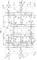
- FIG. 1 illustrates a memory bank 10 of a prior art semiconductor memory utilizing a hierarchical bit line architecture.
- the memory bank is divided into subarrays of memory cells, e.g., MAa to MAd, and a number of sense amplifier banks such as 12 j , 12 j+1 , 12 j+2 .
- the sense amplifiers SA i within each sense amplifier bank are arranged in a shared configuration, such that each sense amplifier amplifies signals from memory cells on both sides thereof in a time multiplexed manner.
- Each subarray has N columns C 1 -C N ; however, since the sense amplifiers are shared, each SA bank has N/2 sense amplifiers.
- Each sense amplifier e.g., SA 2 of bank 12 j+1 is connected on each side to a master bit line pair consisting of a true master bit line MBL and a complementary master bit line MBL .
- each true master bit line MBL is connected to four true local bit lines LBL 1 to LBL 4 of equal length L
- each complementary master bit line MBL is connected to four complementary local bit lines LBL 1 to LBL 4 .
- the sense amplifier amplifies a differential voltage between the pair of master bit lines -- one master bit line is used to carry a reference voltage while the other carries a cell signal transferred thereto by activation of a selected memory cell MC.
- a word line WL j in the jth row is activated in accordance with the row address to access the selected memory cell.
- the configuration shown is known as a folded bit line architecture, wherein the true and complementary bit lines run side by side one another in close proximity. If an open bit line configuration were used, the complementary master bit line would reside on the opposite side of the sense amplifier as the true master
- FET switches S are each coupled between an end portion of a respective local bit line and a connection point P connecting the corresponding master bit line.
- Memory cells coupled to a particular local bit line are accessed by closing the corresponding switch S and opening the other switches in the corresponding column by appropriate control voltages on control lines 23 1 -23 4 .
- bit line capacitance is proportional to bit line length. As such, bit line length is limited by the maximum bit line capacitance that can be tolerated. The maximum capacitance is generally determined by the allowable sensing margin and the power dissipation.
- the master bit line capacitance per unit length is less than the local bit line capacitance per unit length, since the local bit lines are directly coupled to the memory cells which significantly contribute to the local bit line capacitance, whereas the master bit lines are not directly coupled to the cells.
- the total capacitance can be significantly less than in a non-hierarchical layout (i.e., layouts with only one layer of bit lines, each extending the entire column length and directly coupled to the memory cells).
- the architecture permits each sense amplifier to be used for more cells, coupled to the local bit lines and one long master bit line, thereby reducing the number of sense amplifiers per chip. A smaller chip size is thus possible, provided that the area allocated to the switches S and additional control circuitry does not exceed the area saved by reducing the number of sense amplifiers.
- FIG. 2 illustrates a variation of the above-discussed hierarchical bit line architecture.
- the shown configuration will be referred to hereafter as a "hybrid" type hierarchical architecture.
- FIG. 2 shows the case in which only two local bit line pairs (LB1 1 , LBL 1 ) and (LBL 2 , LBL 2 ) are disposed on each side of an associated sense amplifier SA i .
- the local bit lines nearest the sense amplifier i.e., LBL 1 and LBL 1 , are connected to the drain or source of a respective switch 25 1 , with the other side of the switch connecting directly to the sense amplifier electronics at a circuit node 63.
- This circuit node 63 is generally the same circuit node that connects the sense amplifier electronics to the corresponding master bit line MBL or MBL .
- a switch 25 2 is coupled between each far side local bit line LBL 2 and LBL 2 and the corresponding master bit line at a connection node d. Gaps g separate LBL 1 from LBL 2 and LBL 1 , from LBL 2 . To access a memory cell MC coupled to LBL 1 or LBL 1 , switches 25 1 are turned on (closed) while switches 25 2 are off, and vice versa to access cells coupled to the far side local bit lines LBL 2 and LBL 2 .
- memory cells coupled to the far side local bit lines are operatively coupled to the sense amplifier via the far side local bit line and the master bit line, whereas those cells coupled to the near side local bit line are coupled to the sense amplifier only via the near side local bit line.
- the configuration of FIG. 2 is referred to as a hybrid. If more than two local bit line pairs are used on each side of the sense amplifier, then the path connecting the memory cells coupled to the near-side local bit lines LBL 1 and LBL 1 consists of only the local bit line whereas the paths connecting the sense amplifier to the other memory cells in the column consists of the master bit line in series with the respective local bit line.
- the present invention is directed towards a semiconductor memory having a hierarchical bit line architecture in which local bit lines disposed in any given column are coupled to different numbers of memory cells in order to substantially equalize total bit line capacitance with respect to any of the memory cells, thus improving data retention time for the memory.
- a semiconductor memory in accordance with the present invention includes a plurality of rows and columns, where each column has a sense amplifier with a master bit line operatively coupled thereto.
- a plurality of local bit lines are disposed in each column, each coupled to plural memory cells, vertically spaced from the master bit line, and selectively coupled to the sense amplifier. At least one of the local bit lines in the column is selectively coupled to the sense amplifier via the master bit line. At least a first one of the local bit lines in the column is coupled to a different number of memory cells than at least a second one of the local bit lines in the column.
- a hybrid-type hierarchical bit line configuration is employed in which a near side local bit line is directly coupled to the sense amplifier via a switch, and one or more far side local bit lines in the column are operatively coupled to the sense amplifier via the master bit line.
- the near side local bit line is coupled to more memory cells than the other local bit line(s) in the column.
- the present invention relates to an improved hierarchical bit line architecture for semiconductor memories.
- the invention provides a way to equalize total bit line capacitance, thereby improving retention time for the memory cells in the array.
- an exemplary embodiment of the invention is described in the context of a DRAM chip.
- the invention however has broader applications.
- the invention has application in other memory devices such as EDO-DRAM, SDRAM, RAMBUS-DRAM, SLDRAM, MDRAM, SRAM, flash RAM, EPROM, EEPROM, mask ROM, or merged DRAM-logic (embedded DRAM).
- the total bit line capacitance with respect to the cells coupled to LBL 1 is just the local bit line capacitance of LBL 1 , i.e., "C LBL1 ".
- the total bit line capacitance with respect to the cells coupled to LBL 2 is the local bit line capacitance of LBL 2 plus the master bit line capacitance, i.e., "C LBL2+MBL ".
- the average power consumption during sensing is smaller than in the standard hierarchical architecture (non-hybrid architecture as in FIG. 1).
- the data retention time "t ret " of a memory cell is, to a first order, proportional to 1/C BL where C BL is the total bit line capacitance.
- the data retention time of the cells coupled to LBL 2 i.e., "t ret LBL2+MBL "
- t ret LBL1 the data retention time of the cells coupled to LBL 1
- C LBL2+MBL the total bit line capacitance
- the retention time of a chip is not defined as one half the sum of these two retention times, but rather, as the smaller of the two retention times, which is t ret LBL2+MBL .
- the smaller retention time for the cells coupled to LBL 2 degrades the overall retention time for the chip.
- at least two local bit lines within a master bit line is provided with different lengths.
- the capacitances of the local bit lines are affected by the master bit line.
- the contribution of capacitance by the master bit line varies according to the location of a local bit line within the master bit line.
- Providing at least two local bit lines with different lengths offsets the difference in capacitance contributed by the master bit line to the different local bit lines.
- the variances in capacitance between the local bit lines are reduced, resulting in more uniform retention time among the cells of the different local bit lines.
- far side local bit line LBL 2 comprises a length L2, which is shorter than the length L1 of the near side bit line LBL 1 ,. That is, the near side bit line LBL 1 , is coupled to more memory cells MC than the far side local bit line LBL 2 .
- the term "length" of a local bit line refers to the distance in the column direction of the local bit line over the memory cells it is coupled to, and not to additional wiring lengths from the last memory cell to an external connection point.
- an LBL with a longer length than another LBL is defined herein as being coupled to more memory cells of the same size).
- the lengths L1 and L2 are designed to equalize the total bit line capacitance with respect to the cells coupled to LBL 1 and LBL 2 .
- bit line structure 18 of FIG. 3 exhibits a 12% improvement in data retention time as compared to the prior art hybrid approach of FIG. 2.
- Bit line structure 18 also differs from the configuration of FIG. 2 in that the far side bit line switches 25 2 are moved in proximity to the sense amplifier SA i .
- Switches 25 2 are each disposed between the associated master bit line MBL or MBL and the connection node 63 within the sense amplifier. Opening the switches 25 2 disconnects the master bit line pair from the sense amplifier, allowing the cells coupled to LBL 1 or LBL 1 to be accessed by closing switches 25 1 . Positioning the switches 25 2 in proximity to the sense amplifier in this manner removes all the switches from the memory cell array area (for the case of two local bit lines per one master bit line as in FIG. 3).
- Memory bank 20 includes sense amplifier (SA) banks, e.g. 27 i-1 , 27 i , 27 i+1 , with sense amplifiers arranged in an interleaved configuration and with local bit lines of unequal length to improve data retention time as discussed above.
- SA sense amplifier
- each local bit line LBL 1L or LBL 1R on the near side of an associated sense amplifier is longer than the length L2 of a local bit line LBL 2L or LBL 2R on the far side of an associated sense amplifier, to equalize the total bit line capacitance and hence, the data retention times.
- the subscript "L” is used to refer to the left hand side of the associated sense amplifier and the subscript "R” refers to the right hand side).
- sense amplifier SA 2 of SA bank: 27 i amplifies and refreshes cell signals from memory cells in memory subarray MAb via local bit line pair LBL 1L , LBL 1 L directly, or from pair LBL 2L , LBL 2L via MBL L , MBL L , respectively.
- the source or drain of switch 25 1 on the other side of LBL 1L connects to the source or drain of switch 25 2 at a common circuit node 63 within SA 2 (where the other side of switch 25 2 connects to MBL L ).
- the switch 25 1 coupled to LBL 1R and the switch 25 2 coupled to MBL R also connect to a common circuit node 63. Switches 25 1 are closed to access cells coupled to LBL 1L while switches 25 2 are open, and vice versa to access cells coupled to LBL 2L .
- Control lines 23 1 to 23 4 are selectively activated by suitable control electronics known in the art, to open or close the desired switches 25 1 and 25 2 in accordance with the row address.
- Word lines as WL i in the "ith" row are selectively activated in a conventional manner to activate the particular memory cell MC to be accessed.
- the memory cells on the opposite side of SA 2 i.e., in memory subarray MAc, are accessed in the same manner, either directly through local bit lines LBL 1R , LBL 1 R and switches 25 1 or through LBL 2R , LBL 1 R and switches 25 2 via MBL R and MBL R , respectively.
- the sense amplifiers are interleaved in a column to column fashion so that, for example, memory cells in odd columns C 1 , C 3 , etc., of subarrays MAa and MAb are accessed via SA bank: 27 i-1 ; SA bank 27 i is used to access even columns of MAb and MAc; SA bank 27 i+1 is used to access odd columns of MAc and MAd, and so forth.
- FIG. 5 schematically illustrates exemplary circuitry within one of the shared sense amplifiers SA i of column C i .
- a latch circuit 54 On each side of a latch circuit 54 there resides a pair of multiplex switches 53 1L , 53 2L or 53 1R , 53 2R to select the memory subarray MAa or MAb on the respective left or right sides of the sense amplifier in response to control signals MUX L or MUX R , respectively.
- a control signal CTL P controls the P-latch portion of latch 54 while control signal CTL N controls the N-latch.
- Equalization circuits 55 L and 55 R are coupled between the MUX switches 53 and the memory subarrays MAa and MAb, respectively.
- Control lines 56 carry precharge and control voltages to each equalization circuit 55 L , 55 R in a conventional manner.
- Column select switches (not shown) are also part of the sense amplifier circuitry, as is conventional, to select the desired column to be accessed in accordance with the column address.
- LBL select switches 25 1 and 25 2 are each connected to a circuit point 63 as shown in proximity to each equalization circuit 55 L and 55 R .
- the other side (source or drain) of each switch 25 2 connects to the corresponding master bit line by means of a via hole connection V 1 .
- the opposite side of each switch 25 1 connects to the associated local bit line by means of a via hole connection V 2 .
- Switchches 25 1 and 25 2 are disposed at the wafer level whereas the local bit lines and master bit lines are disposed on higher fabirication levels -- as such, inter-level via hole connections are necessary to connect the switches to the bit lines).
- FIG. 6 shows another embodiment of the present invention, designated as 100, which utilizes more than two local bit line pairs on a single side of a sense amplifier SA i .
- a sense amplifier SA i which utilizes more than two local bit line pairs on a single side of a sense amplifier SA i .
- four local bit line pairs, LBL 1 , LBL 1 to LBL 4 , LBL 4 are used.
- the local bit lines nearest the sense amplifier, i.e., LBL 1 , and LBL 1 have a length of L1 whereas each of the other local bit lines has a shorter length L2.
- the relationship between L1 and L2 may be designed such that the total bit line capacitance with respect to all memory cells is the same.
- the total bit line capacitance for cells connected to LBL 1 is just the local bit line capacitance of LBL 1 whereas the total bit line capacitance for the cells connected to any of LBL 2 to LBL 4 is the capacitance of that local bit line plus the master bit line capacitance, which is to first order the same for all such memory cells. Also, by making LBL 1 and LBL 1 longer than the other local bit lines, a substantial increase in data retention time can be realized, analogous to the retention time improvement described above for the case of only two local bit lines per master bit line.
- local bit line switches 25 1 to 25 4 control the access of memory cells coupled to local bit line pairs LBL 1 , LBL 1 to LBL 4 , LBL 4 , respectively.
- An additional pair of switches 35 is added in between each master bit line and the respective connection point 63 within the sense amplifier. These switches are open whenever switches 25 1 are closed to access cells coupled to LBL 1 or LBL 1 , and are closed to access any of the cells coupled to the other LBLs. Switches 35 are controlled by control voltages on a control line 36. The inclusion of switches 35 serves to remove the effect of the master bit line capacitance whenever cells coupled to LBL 1 or LBL 1 are accessed.
- FIG. 7 yet another embodiment 200 of the invention is illustrated, which utilizes a hierarchical, hybrid-type open bit line configuration.
- the local bit lines in any given column have unequal lengths as in the embodiments described above.
- the true/complementary bit line pairs do not run side by side one another on the same side of each sense amplifier. Instead, the true bit line of a bit line pair runs on one side of the associated sense amplifier and the complementary bit line of the pair runs on the opposite side of the associated sense amplifier.
- the complementary line on the opposite side is used to supply a precharge reference voltage to the sense amplifier, whereby the sense amplifier performs differential amplification of the difference voltage between the true and complementary lines.
- the true bit line is used to supply the precharge reference voltage to the sense amplifier.
- memory bank 200 which may be part of a DRAM chip, for example, includes sense amplifier banks such as 42 j-1 to 42 j+1 each arranged in between two of memory subarrays MAa-MAd.
- Each sense amplifier such as SA 2 of SA bank 42 j connects on a left side thereof to a pair of switches 25 1 , 25 2 , where switch 25 1 is connected in series with local bit line LBL 1L and switch 25 2 connects in series with a master bit line MBL that connects directly to local bit line LBL 2 at node d.
- Switches 25 1 and 25 2 are connected at circuit node 63 within the sense amplifier.
- LBL 1 is directly connected to the sense amplifier via a switch 25 1
- LBL 2 is operably connected to the sense amplifier via master bit line MBL and switch 25 2 .
- switches 25 1 on both sides of SA 2 are closed, and switches 25 2 on both sides of SA 2 are opened.
- the opposite switching conditions are implemented to access cells coupled to LBL 2 or LBL 2 .
- the length L1 of LBL 1 and LBL 1 is longer than the length L2 of LBL 2 and LBL 2 in order to achieve an increase in data retention time for the memory, analogous to that described above for the folded bit line architecture.
- the sense amplifier circuitry is similar to that described above with respect to FIG. 5, except that multiplex switches are omitted, and only one equalization circuit is needed.
- the open bit line configuration of FIG. 7 may be modified by employing more than two local bit lines per master bit line on each side of the sense amplifier, e.g., four LBLs per MBL, analogous to the folded bit line embodiment discussed above in reference to FIG. 6.
- the present invention is also applicable to memory cell arrays with sense amplifiers using reference cells, such as in flash RAM.
- the bit lines are not arranged in true and complementary pairs.
- the reference cell within the sense amplifier provides the equalization (reference) voltage that the complementary line would otherwise provide (when accessing cells coupled to the true cells) or that the true bit line would otherwise provide (when accessing cells coupled to the complementary bit lines).
- the memory array may look essentially the same as shown in FIG. 7, except that the MBLs and LBLs on opposite sides of a common sense amplifier do not operate in pairs, but instead operate independently.
- multiplex switches are used within the sense amplifier circuitry to select the left or right side of the sense amplifier for memory cell access.
- the local bit lines coupled to any given sense amplifier would be of unequal lengths, i.e., the far side local bit line being shorter than the near side local bit line, to improve data retention time.
- the present invention has been described in the embodiments above as being applicable to a hybrid-type hierarchical architecture, the invention may also have utility in a non-hybrid type hierarchical architecture similar to that shown in FIG. 1.
- the prior art configuration shown can be modified in accordance with the present invention by employing a different length for the local bit lines LBL 4 , LBL 4 furthest from the sense amplifier than for the other local bit lines.
- the last local bit line LBL 4 has a different bit line capacitance per unit length than the other local bit lines in the same column because the master bit line MBL in that column does not run directly atop LBL 4 .
- the length of LBL 4 the total capacitance with respect to the memory cells coupled to LBL 4 can be substantially equalized with respect to the other memory cells, thereby improving retention time for the overall memory.
Abstract
Description
Claims (21)
- A semiconductor memory having a plurality of rows and columns, comprising:at least one sense amplifier in each column;a master bit line operatively coupled to the sense amplifier;a plurality of local bit lines disposed in each column, each coupled to memory cells and vertically spaced from the master bit line in the column and selectively coupled to the sense amplifier, with at least one of the local bit lines being selectively coupled to the sense amplifier via the master bit line;
wherein at least a first one of the local bit lines is coupled to a different number of said memory cells than at least a second one of the local bit lines. - The semiconductor memory of claim 1 wherein the local bit lines of each column include a near side local bit line selectively coupled directly to the sense amplifier via a first switch, and a far side local bit line selectively coupled to the sense amplifier via the master bit line and a second switch;
wherein the near side local bit line is coupled to a different number of memory cells than the far side local bit line, and has a different length in the column direction over the respective memory cells than the far side local bit line. - The semiconductor memory of claim 2 wherein the near side local bit line is coupled to a larger number of memory cells than the far side local bit line, and has a longer length in the column direction over the respective memory cells than the far side local bit line.
- The semiconductor memory of claim 2 wherein said plurality of local bit lines in each column comprise one near side local bit line and one far side local bit line, each operatively coupled to the associated sense amplifier on one side thereof.
- The semiconductor memory of claim 2 wherein said second switch is coupled between at least a portion of the master bit line and the sense amplifier.
- The semiconductor memory of claim 1 wherein each sense amplifier is arranged in a shared configuration.
- The semiconductor memory of claim 1 wherein each column includes a true master bit line coupled to at least one true local bit line, and a complementary master bit line coupled to at least one complementary local bit line.
- The semiconductor memory of claim 7 wherein the true and complementary master and local bit lines are arranged in a folded bit line configuration.
- The semiconductor memory of claim 7 wherein the true and complementary master and local bit lines are arranged in an open bit line configuration.
- The semiconductor memory of claim 1 wherein said different number of memory cells are selected such that total bit line capacitance with respect to all the memory cells in the memory is substantially equalized.
- The semiconductor memory of claim 1 wherein the local bit lines of each column include a near side local bit line selectively coupled directly to the sense amplifier via a first switch, and a plurality of far side local bit lines selectively coupled to the sense amplifier via the master bit line and a plurality of additional switches.
- The semiconductor memory of claim 11 wherein said plurality of additional switches comprises a second switch coupled between said master bit line and said sense amplifier, and a plurality of local bit line switches, each coupled between an associated far side local bit line and said master bit line.
- A semiconductor memory having a plurality of rows and columns, comprising:at least one sense amplifier in each column;a master bit line operatively coupled to the sense amplifier;a plurality of local bit lines disposed in each column, each coupled to memory cells and vertically spaced from the master bit line in the column and selectively coupled to the sense amplifier, said plurality of local bit lines including a near side local bit line selectively coupled to the sense amplifier via a first switch coupled therebetween, and at least one far side local bit line selectively coupled to the sense amplifier via the master bit line and a second switch coupled between the master bit line and the sense amplifier;
wherein the near side local bit line is coupled to a larger number of memory cells than any of said at least one far side local bit line. - The semiconductor memory of claim 13 wherein said at least one sense amplifier is arranged in a shared configuration between memory cell subarrays on each side thereof and with a master bit line pair and a plurality of local bit line pairs on each side thereof in a folded configuration.
- The semiconductor memory of claim 13 wherein said at least one sense amplifier is arranged in a shared configuration between memory cell subarrays on each side thereof, and with master and local bit lines on each side thereof arranged in an open bit line configuration.
- The semiconductor memory of claim 13 wherein each master bit line is directly coupled to a single far side local bit line.
- The semiconductor memory of claim 13 wherein said larger number of memory cells are selected such that total bit line capacitance with respect to all the memory cells in the memory is substantially equalized.
- A semiconductor memory having a plurality of rows and columns, comprising:at least one sense amplifier in each column;a master bit line operatively coupled to the sense amplifier;a plurality of local bit lines disposed in each column, each coupled to memory cells and vertically spaced from the master bit line in the column and selectively coupled to the sense amplifier, said plurality of local bit lines including a near side local bit line selectively coupled to the sense amplifier via a first switch coupled therebetween, and a plurality of far side local bit lines, each selectively coupled to the sense amplifier via the master bit line and a plurality of additional switches;said plurality of additional switches comprising a second switch coupled between the master bit line and the sense amplifier and a local bit line switch coupled between each far side local bit line and the master bit line;
wherein the near side local bit line is coupled to a larger number of memory cells than each of the far side local bit lines. - The semiconductor memory of claim 18 wherein said larger number of memory cells are selected such that total bit line capacitance with respect to all the memory cells in the memory is substantially equalized.
- The semiconductor memory of claim 18 including master and local bit lines arranged in one of an open or folded bit line configuration.
- A semiconductor memory having a plurality of rows and columns, the memory comprising:a master bit line within a column, the master bit line comprising a plurality of local bit lines disposed therein, wherein the at least two of the plurality of local bit lines are of different lengths.
Applications Claiming Priority (2)
| Application Number | Priority Date | Filing Date | Title |
|---|---|---|---|
| US08/942,275 US5966315A (en) | 1997-09-30 | 1997-09-30 | Semiconductor memory having hierarchical bit line architecture with non-uniform local bit lines |
| US942275 | 1997-09-30 |
Publications (3)
| Publication Number | Publication Date |
|---|---|
| EP0905701A2 true EP0905701A2 (en) | 1999-03-31 |
| EP0905701A3 EP0905701A3 (en) | 1999-12-08 |
| EP0905701B1 EP0905701B1 (en) | 2005-11-30 |
Family
ID=25477844
Family Applications (1)
| Application Number | Title | Priority Date | Filing Date |
|---|---|---|---|
| EP98116745A Expired - Lifetime EP0905701B1 (en) | 1997-09-30 | 1998-09-04 | Semiconductor memory having hierarchical bit line architecture with non-uniform local bit lines |
Country Status (7)
| Country | Link |
|---|---|
| US (1) | US5966315A (en) |
| EP (1) | EP0905701B1 (en) |
| JP (1) | JPH11167792A (en) |
| KR (1) | KR100575044B1 (en) |
| CN (1) | CN1124610C (en) |
| DE (1) | DE69832566T2 (en) |
| TW (1) | TW410350B (en) |
Cited By (2)
| Publication number | Priority date | Publication date | Assignee | Title |
|---|---|---|---|---|
| DE10004109A1 (en) * | 2000-01-31 | 2001-08-09 | Infineon Technologies Ag | Memory module of electronic data processor, has switch connecting main and local data lines, arranged such that delay time of bit during synchronous memory access is made shorter |
| WO2022250897A1 (en) * | 2021-05-28 | 2022-12-01 | Microsoft Technology Licensing, Llc | Memory having flying bitlines for improved burst mode read operations |
Families Citing this family (41)
| Publication number | Priority date | Publication date | Assignee | Title |
|---|---|---|---|---|
| US6154864A (en) * | 1998-05-19 | 2000-11-28 | Micron Technology, Inc. | Read only memory embedded in a dynamic random access memory |
| US6018489A (en) * | 1998-09-17 | 2000-01-25 | Vanguard International Semiconductor Corporation | Mock wordline scheme for timing control |
| US6333866B1 (en) * | 1998-09-28 | 2001-12-25 | Texas Instruments Incorporated | Semiconductor device array having dense memory cell array and heirarchical bit line scheme |
| DE19944738C2 (en) * | 1999-09-17 | 2001-08-02 | Infineon Technologies Ag | Segmented word line architecture for dividing a word line into several banks for cell arrays with long bit lines |
| GB2363231B (en) * | 1999-09-24 | 2002-05-08 | Clearspeed Technology Ltd | Memory devices |
| JP4936582B2 (en) * | 2000-07-28 | 2012-05-23 | ルネサスエレクトロニクス株式会社 | Semiconductor memory device |
| DE10121837C1 (en) * | 2001-05-04 | 2002-12-05 | Infineon Technologies Ag | Memory circuit with multiple memory areas |
| US6603693B2 (en) | 2001-12-12 | 2003-08-05 | Micron Technology, Inc. | DRAM with bias sensing |
| US6545899B1 (en) | 2001-12-12 | 2003-04-08 | Micron Technology, Inc. | ROM embedded DRAM with bias sensing |
| US6747889B2 (en) * | 2001-12-12 | 2004-06-08 | Micron Technology, Inc. | Half density ROM embedded DRAM |
| US20030115538A1 (en) * | 2001-12-13 | 2003-06-19 | Micron Technology, Inc. | Error correction in ROM embedded DRAM |
| US20030185062A1 (en) * | 2002-03-28 | 2003-10-02 | Micron Technology, Inc. | Proximity lookup for large arrays |
| US6785167B2 (en) * | 2002-06-18 | 2004-08-31 | Micron Technology, Inc. | ROM embedded DRAM with programming |
| US6781867B2 (en) * | 2002-07-11 | 2004-08-24 | Micron Technology, Inc. | Embedded ROM device using substrate leakage |
| US6865100B2 (en) * | 2002-08-12 | 2005-03-08 | Micron Technology, Inc. | 6F2 architecture ROM embedded DRAM |
| US7174477B2 (en) * | 2003-02-04 | 2007-02-06 | Micron Technology, Inc. | ROM redundancy in ROM embedded DRAM |
| KR100612953B1 (en) * | 2004-03-31 | 2006-08-14 | 주식회사 하이닉스반도체 | Semiconductor memory device for high speed of bit-lines |
| KR100600056B1 (en) | 2004-10-30 | 2006-07-13 | 주식회사 하이닉스반도체 | Semiconductor device for low voltage |
| US7088638B1 (en) | 2005-02-09 | 2006-08-08 | International Business Machines Corporation | Global and local read control synchronization method and system for a memory array configured with multiple memory subarrays |
| DE102006010762B3 (en) * | 2006-03-08 | 2007-10-04 | Infineon Technologies Ag | Integrated semiconductor memory |
| KR100780954B1 (en) | 2006-08-04 | 2007-12-03 | 삼성전자주식회사 | Sense amplifier and semiconductor memory device comprising it, and data sensing method |
| US20080031029A1 (en) * | 2006-08-05 | 2008-02-07 | Taiwan Semiconductor Manufacturing Co., Ltd. | Semiconductor memory device with split bit-line structure |
| DE102007012902B3 (en) * | 2007-03-19 | 2008-07-10 | Qimonda Ag | Bit line pair and amplifier arrangement for use in e.g. dynamic RAM, of computer system, has read amplifiers whose positions along bit line direction are selected such that coupling paths have same coupling characteristics |
| US8144537B2 (en) * | 2008-11-11 | 2012-03-27 | Stmicroelectronics Pvt. Ltd. | Balanced sense amplifier for single ended bitline memory architecture |
| US8050127B2 (en) * | 2009-02-06 | 2011-11-01 | Hynix Semiconductor Inc. | Semiconductor memory device |
| JP2010192052A (en) * | 2009-02-19 | 2010-09-02 | Hitachi Ulsi Systems Co Ltd | Semiconductor device |
| TW201142869A (en) * | 2010-02-09 | 2011-12-01 | Samsung Electronics Co Ltd | Memory device from which dummy edge memory block is removed |
| US9275721B2 (en) * | 2010-07-30 | 2016-03-01 | Taiwan Semiconductor Manufacturing Company, Ltd. | Split bit line architecture circuits and methods for memory devices |
| KR102393976B1 (en) | 2015-05-20 | 2022-05-04 | 삼성전자주식회사 | Semiconductor memory devices |
| US9601162B1 (en) | 2015-09-10 | 2017-03-21 | Taiwan Semiconductor Manufacturing Co., Ltd. | Memory devices with strap cells |
| US9659635B1 (en) * | 2016-01-29 | 2017-05-23 | Taiwan Semiconductor Manufacturing Company, Ltd. | Memory array with bit-lines connected to different sub-arrays through jumper structures |
| US10964683B2 (en) * | 2017-08-30 | 2021-03-30 | Taiwan Semiconductor Manufacturing Company, Ltd. | Memory array circuit and method of manufacturing the same |
| US10776277B2 (en) | 2017-10-31 | 2020-09-15 | Sandisk Technologies Llc | Partial memory die with inter-plane re-mapping |
| US10290354B1 (en) | 2017-10-31 | 2019-05-14 | Sandisk Technologies Llc | Partial memory die |
| US10854619B2 (en) | 2018-12-07 | 2020-12-01 | Sandisk Technologies Llc | Three-dimensional memory device containing bit line switches |
| US10734080B2 (en) | 2018-12-07 | 2020-08-04 | Sandisk Technologies Llc | Three-dimensional memory device containing bit line switches |
| US10741535B1 (en) | 2019-02-14 | 2020-08-11 | Sandisk Technologies Llc | Bonded assembly containing multiple memory dies sharing peripheral circuitry on a support die and methods for making the same |
| US10879260B2 (en) | 2019-02-28 | 2020-12-29 | Sandisk Technologies Llc | Bonded assembly of a support die and plural memory dies containing laterally shifted vertical interconnections and methods for making the same |
| DE102020105669A1 (en) | 2019-12-31 | 2021-07-01 | Taiwan Semiconductor Manufacturing Co., Ltd. | INTEGRATED CIRCUIT |
| CN113129944A (en) | 2019-12-31 | 2021-07-16 | 台湾积体电路制造股份有限公司 | Integrated circuit and method thereof |
| US11631690B2 (en) | 2020-12-15 | 2023-04-18 | Sandisk Technologies Llc | Three-dimensional memory device including trench-isolated memory planes and method of making the same |
Citations (2)
| Publication number | Priority date | Publication date | Assignee | Title |
|---|---|---|---|---|
| US4636988A (en) * | 1985-01-07 | 1987-01-13 | Thomson Components-Mostek Corporation | CMOS memory arrangement with reduced data line compacitance |
| US5610871A (en) * | 1993-11-30 | 1997-03-11 | Mitsubishi Denki Kabushiki Kaisha | Semiconductor memory device having a hierarchical bit line structure with reduced interference noise |
Family Cites Families (3)
| Publication number | Priority date | Publication date | Assignee | Title |
|---|---|---|---|---|
| JP3626510B2 (en) * | 1993-04-13 | 2005-03-09 | 株式会社ルネサステクノロジ | Semiconductor memory device |
| JP4179402B2 (en) * | 1996-02-15 | 2008-11-12 | 富士通マイクロエレクトロニクス株式会社 | Semiconductor memory device |
| KR0166046B1 (en) * | 1995-10-06 | 1999-02-01 | 김주용 | Semiconductor memory device with hierarchical bit line structure |
-
1997
- 1997-09-30 US US08/942,275 patent/US5966315A/en not_active Expired - Lifetime
-
1998
- 1998-09-04 DE DE69832566T patent/DE69832566T2/en not_active Expired - Lifetime
- 1998-09-04 EP EP98116745A patent/EP0905701B1/en not_active Expired - Lifetime
- 1998-09-25 CN CN98120719A patent/CN1124610C/en not_active Expired - Fee Related
- 1998-09-29 JP JP10276135A patent/JPH11167792A/en active Pending
- 1998-09-30 KR KR1019980040801A patent/KR100575044B1/en not_active IP Right Cessation
- 1998-09-30 TW TW087116164A patent/TW410350B/en not_active IP Right Cessation
Patent Citations (2)
| Publication number | Priority date | Publication date | Assignee | Title |
|---|---|---|---|---|
| US4636988A (en) * | 1985-01-07 | 1987-01-13 | Thomson Components-Mostek Corporation | CMOS memory arrangement with reduced data line compacitance |
| US5610871A (en) * | 1993-11-30 | 1997-03-11 | Mitsubishi Denki Kabushiki Kaisha | Semiconductor memory device having a hierarchical bit line structure with reduced interference noise |
Cited By (5)
| Publication number | Priority date | Publication date | Assignee | Title |
|---|---|---|---|---|
| DE10004109A1 (en) * | 2000-01-31 | 2001-08-09 | Infineon Technologies Ag | Memory module of electronic data processor, has switch connecting main and local data lines, arranged such that delay time of bit during synchronous memory access is made shorter |
| DE10004109C2 (en) * | 2000-01-31 | 2001-11-29 | Infineon Technologies Ag | Memory module with short access time |
| US6388944B2 (en) | 2000-01-31 | 2002-05-14 | Infineon Technologies Ag | Memory component with short access time |
| WO2022250897A1 (en) * | 2021-05-28 | 2022-12-01 | Microsoft Technology Licensing, Llc | Memory having flying bitlines for improved burst mode read operations |
| US11587610B2 (en) | 2021-05-28 | 2023-02-21 | Microsoft Technology Licensing, Llc | Memory having flying bitlines for improved burst mode read operations |
Also Published As
| Publication number | Publication date |
|---|---|
| EP0905701A3 (en) | 1999-12-08 |
| US5966315A (en) | 1999-10-12 |
| DE69832566D1 (en) | 2006-01-05 |
| CN1124610C (en) | 2003-10-15 |
| JPH11167792A (en) | 1999-06-22 |
| EP0905701B1 (en) | 2005-11-30 |
| DE69832566T2 (en) | 2006-08-10 |
| KR100575044B1 (en) | 2006-10-25 |
| KR19990030297A (en) | 1999-04-26 |
| CN1218960A (en) | 1999-06-09 |
| TW410350B (en) | 2000-11-01 |
Similar Documents
| Publication | Publication Date | Title |
|---|---|---|
| EP0905701B1 (en) | Semiconductor memory having hierarchical bit line architecture with non-uniform local bit lines | |
| US5923605A (en) | Space-efficient semiconductor memory having hierarchical column select line architecture | |
| US5917744A (en) | Semiconductor memory having hierarchical bit line architecture with interleaved master bitlines | |
| US5825704A (en) | High performance embedded semiconductor memory devices with multiple dimension first-level bit lines | |
| US6404670B2 (en) | Multiple ports memory-cell structure | |
| US8218386B2 (en) | Embedded memory databus architecture | |
| KR100887333B1 (en) | Semiconductor memory | |
| US6069815A (en) | Semiconductor memory having hierarchical bit line and/or word line architecture | |
| US6108229A (en) | High performance embedded semiconductor memory device with multiple dimension first-level bit-lines | |
| US6504745B2 (en) | High performance erasable programmable read-only memory (EPROM) devices with multiple dimension first-level bit lines | |
| US6496442B2 (en) | Dynamic random access memory device and semiconductor integrated circuit device | |
| US6456521B1 (en) | Hierarchical bitline DRAM architecture system | |
| US20110096584A1 (en) | Semiconductor device having open bit line architecture | |
| US20030020097A1 (en) | Memory device with divided bit-line architecture | |
| US7215595B2 (en) | Memory device and method using a sense amplifier as a cache | |
| KR100288819B1 (en) | Semiconductor memory device | |
| JP3159496B2 (en) | Semiconductor memory device | |
| US7324396B2 (en) | Sense amplifier organization for twin cell memory devices | |
| US6621752B2 (en) | Refreshing scheme for memory cells a memory array to increase performance of integrated circuits | |
| US20040013013A1 (en) | Memory, module with crossed bit lines, and method for reading the memory module | |
| CA2313951A1 (en) | Scheme for accelerating bit line equalization in a high speed dram architecture |
Legal Events
| Date | Code | Title | Description |
|---|---|---|---|
| PUAI | Public reference made under article 153(3) epc to a published international application that has entered the european phase |
Free format text: ORIGINAL CODE: 0009012 |
|
| AK | Designated contracting states |
Kind code of ref document: A2 Designated state(s): DE FR GB IE IT NL |
|
| AX | Request for extension of the european patent |
Free format text: AL;LT;LV;MK;RO;SI |
|
| PUAL | Search report despatched |
Free format text: ORIGINAL CODE: 0009013 |
|
| AK | Designated contracting states |
Kind code of ref document: A3 Designated state(s): AT BE CH CY DE DK ES FI FR GB GR IE IT LI LU MC NL PT SE |
|
| AX | Request for extension of the european patent |
Free format text: AL;LT;LV;MK;RO;SI |
|
| 17P | Request for examination filed |
Effective date: 20000309 |
|
| RIN1 | Information on inventor provided before grant (corrected) |
Inventor name: HOENIGSCHMID, HEINZ Inventor name: MUELLER, GERHARD |
|
| AKX | Designation fees paid |
Free format text: DE FR GB IE IT NL |
|
| 17Q | First examination report despatched |
Effective date: 20040310 |
|
| RAP1 | Party data changed (applicant data changed or rights of an application transferred) |
Owner name: INFINEON TECHNOLOGIES AG |
|
| GRAP | Despatch of communication of intention to grant a patent |
Free format text: ORIGINAL CODE: EPIDOSNIGR1 |
|
| RIN1 | Information on inventor provided before grant (corrected) |
Inventor name: HOENIGSCHMID, HEINZ Inventor name: MUELLER, GERHARD |
|
| GRAS | Grant fee paid |
Free format text: ORIGINAL CODE: EPIDOSNIGR3 |
|
| GRAA | (expected) grant |
Free format text: ORIGINAL CODE: 0009210 |
|
| AK | Designated contracting states |
Kind code of ref document: B1 Designated state(s): DE FR GB IE IT NL |
|
| REG | Reference to a national code |
Ref country code: GB Ref legal event code: FG4D |
|
| REG | Reference to a national code |
Ref country code: IE Ref legal event code: FG4D |
|
| REF | Corresponds to: |
Ref document number: 69832566 Country of ref document: DE Date of ref document: 20060105 Kind code of ref document: P |
|
| REG | Reference to a national code |
Ref country code: HK Ref legal event code: WD Ref document number: 1017480 Country of ref document: HK |
|
| ET | Fr: translation filed | ||
| PG25 | Lapsed in a contracting state [announced via postgrant information from national office to epo] |
Ref country code: IE Free format text: LAPSE BECAUSE OF NON-PAYMENT OF DUE FEES Effective date: 20060904 |
|
| PGFP | Annual fee paid to national office [announced via postgrant information from national office to epo] |
Ref country code: GB Payment date: 20060921 Year of fee payment: 9 |
|
| PLBE | No opposition filed within time limit |
Free format text: ORIGINAL CODE: 0009261 |
|
| STAA | Information on the status of an ep patent application or granted ep patent |
Free format text: STATUS: NO OPPOSITION FILED WITHIN TIME LIMIT |
|
| 26N | No opposition filed |
Effective date: 20060831 |
|
| PG25 | Lapsed in a contracting state [announced via postgrant information from national office to epo] |
Ref country code: NL Free format text: LAPSE BECAUSE OF NON-PAYMENT OF DUE FEES Effective date: 20070401 |
|
| NLV4 | Nl: lapsed or anulled due to non-payment of the annual fee |
Effective date: 20070401 |
|
| REG | Reference to a national code |
Ref country code: IE Ref legal event code: MM4A |
|
| GBPC | Gb: european patent ceased through non-payment of renewal fee |
Effective date: 20070904 |
|
| PG25 | Lapsed in a contracting state [announced via postgrant information from national office to epo] |
Ref country code: GB Free format text: LAPSE BECAUSE OF NON-PAYMENT OF DUE FEES Effective date: 20070904 |
|
| REG | Reference to a national code |
Ref country code: FR Ref legal event code: TP Owner name: QIMONDA AG,, DE Effective date: 20120123 |
|
| REG | Reference to a national code |
Ref country code: DE Ref legal event code: R081 Ref document number: 69832566 Country of ref document: DE Owner name: POLARIS INNOVATIONS LTD., IE Free format text: FORMER OWNER: QIMONDA AG, 81739 MUENCHEN, DE Ref country code: DE Ref legal event code: R081 Ref document number: 69832566 Country of ref document: DE Owner name: INFINEON TECHNOLOGIES AG, DE Free format text: FORMER OWNER: QIMONDA AG, 81739 MUENCHEN, DE |
|
| REG | Reference to a national code |
Ref country code: FR Ref legal event code: PLFP Year of fee payment: 18 |
|
| REG | Reference to a national code |
Ref country code: DE Ref legal event code: R081 Ref document number: 69832566 Country of ref document: DE Owner name: POLARIS INNOVATIONS LTD., IE Free format text: FORMER OWNER: INFINEON TECHNOLOGIES AG, 85579 NEUBIBERG, DE |
|
| PGFP | Annual fee paid to national office [announced via postgrant information from national office to epo] |
Ref country code: IT Payment date: 20150930 Year of fee payment: 18 Ref country code: DE Payment date: 20150929 Year of fee payment: 18 |
|
| PGFP | Annual fee paid to national office [announced via postgrant information from national office to epo] |
Ref country code: FR Payment date: 20150925 Year of fee payment: 18 |
|
| REG | Reference to a national code |
Ref country code: FR Ref legal event code: TP Owner name: INFINEON TECHNOLOGIES AG, DE Effective date: 20160212 |
|
| REG | Reference to a national code |
Ref country code: DE Ref legal event code: R119 Ref document number: 69832566 Country of ref document: DE |
|
| REG | Reference to a national code |
Ref country code: FR Ref legal event code: ST Effective date: 20170531 |
|
| PG25 | Lapsed in a contracting state [announced via postgrant information from national office to epo] |
Ref country code: DE Free format text: LAPSE BECAUSE OF NON-PAYMENT OF DUE FEES Effective date: 20170401 Ref country code: FR Free format text: LAPSE BECAUSE OF NON-PAYMENT OF DUE FEES Effective date: 20160930 |
|
| PG25 | Lapsed in a contracting state [announced via postgrant information from national office to epo] |
Ref country code: IT Free format text: LAPSE BECAUSE OF NON-PAYMENT OF DUE FEES Effective date: 20160904 |