EP0907460B1 - Method for chemical-mechanical planarization of stop-on-feature semiconductor wafers - Google Patents
Method for chemical-mechanical planarization of stop-on-feature semiconductor wafers Download PDFInfo
- Publication number
- EP0907460B1 EP0907460B1 EP97927723A EP97927723A EP0907460B1 EP 0907460 B1 EP0907460 B1 EP 0907460B1 EP 97927723 A EP97927723 A EP 97927723A EP 97927723 A EP97927723 A EP 97927723A EP 0907460 B1 EP0907460 B1 EP 0907460B1
- Authority
- EP
- European Patent Office
- Prior art keywords
- wafer
- pad
- slurry
- liquid solution
- layer
- Prior art date
- Legal status (The legal status is an assumption and is not a legal conclusion. Google has not performed a legal analysis and makes no representation as to the accuracy of the status listed.)
- Expired - Lifetime
Links
Images


Classifications
-
- B—PERFORMING OPERATIONS; TRANSPORTING
- B24—GRINDING; POLISHING
- B24B—MACHINES, DEVICES, OR PROCESSES FOR GRINDING OR POLISHING; DRESSING OR CONDITIONING OF ABRADING SURFACES; FEEDING OF GRINDING, POLISHING, OR LAPPING AGENTS
- B24B37/00—Lapping machines or devices; Accessories
- B24B37/04—Lapping machines or devices; Accessories designed for working plane surfaces
-
- B—PERFORMING OPERATIONS; TRANSPORTING
- B24—GRINDING; POLISHING
- B24B—MACHINES, DEVICES, OR PROCESSES FOR GRINDING OR POLISHING; DRESSING OR CONDITIONING OF ABRADING SURFACES; FEEDING OF GRINDING, POLISHING, OR LAPPING AGENTS
- B24B37/00—Lapping machines or devices; Accessories
- B24B37/005—Control means for lapping machines or devices
- B24B37/015—Temperature control
-
- B—PERFORMING OPERATIONS; TRANSPORTING
- B24—GRINDING; POLISHING
- B24B—MACHINES, DEVICES, OR PROCESSES FOR GRINDING OR POLISHING; DRESSING OR CONDITIONING OF ABRADING SURFACES; FEEDING OF GRINDING, POLISHING, OR LAPPING AGENTS
- B24B37/00—Lapping machines or devices; Accessories
- B24B37/04—Lapping machines or devices; Accessories designed for working plane surfaces
- B24B37/07—Lapping machines or devices; Accessories designed for working plane surfaces characterised by the movement of the work or lapping tool
- B24B37/10—Lapping machines or devices; Accessories designed for working plane surfaces characterised by the movement of the work or lapping tool for single side lapping
-
- H—ELECTRICITY
- H01—ELECTRIC ELEMENTS
- H01L—SEMICONDUCTOR DEVICES NOT COVERED BY CLASS H10
- H01L21/00—Processes or apparatus adapted for the manufacture or treatment of semiconductor or solid state devices or of parts thereof
- H01L21/02—Manufacture or treatment of semiconductor devices or of parts thereof
- H01L21/04—Manufacture or treatment of semiconductor devices or of parts thereof the devices having at least one potential-jump barrier or surface barrier, e.g. PN junction, depletion layer or carrier concentration layer
- H01L21/18—Manufacture or treatment of semiconductor devices or of parts thereof the devices having at least one potential-jump barrier or surface barrier, e.g. PN junction, depletion layer or carrier concentration layer the devices having semiconductor bodies comprising elements of Group IV of the Periodic System or AIIIBV compounds with or without impurities, e.g. doping materials
- H01L21/30—Treatment of semiconductor bodies using processes or apparatus not provided for in groups H01L21/20 - H01L21/26
- H01L21/302—Treatment of semiconductor bodies using processes or apparatus not provided for in groups H01L21/20 - H01L21/26 to change their surface-physical characteristics or shape, e.g. etching, polishing, cutting
- H01L21/304—Mechanical treatment, e.g. grinding, polishing, cutting
-
- H—ELECTRICITY
- H01—ELECTRIC ELEMENTS
- H01L—SEMICONDUCTOR DEVICES NOT COVERED BY CLASS H10
- H01L21/00—Processes or apparatus adapted for the manufacture or treatment of semiconductor or solid state devices or of parts thereof
- H01L21/02—Manufacture or treatment of semiconductor devices or of parts thereof
- H01L21/04—Manufacture or treatment of semiconductor devices or of parts thereof the devices having at least one potential-jump barrier or surface barrier, e.g. PN junction, depletion layer or carrier concentration layer
- H01L21/18—Manufacture or treatment of semiconductor devices or of parts thereof the devices having at least one potential-jump barrier or surface barrier, e.g. PN junction, depletion layer or carrier concentration layer the devices having semiconductor bodies comprising elements of Group IV of the Periodic System or AIIIBV compounds with or without impurities, e.g. doping materials
- H01L21/30—Treatment of semiconductor bodies using processes or apparatus not provided for in groups H01L21/20 - H01L21/26
- H01L21/31—Treatment of semiconductor bodies using processes or apparatus not provided for in groups H01L21/20 - H01L21/26 to form insulating layers thereon, e.g. for masking or by using photolithographic techniques; After treatment of these layers; Selection of materials for these layers
- H01L21/3105—After-treatment
- H01L21/31051—Planarisation of the insulating layers
- H01L21/31053—Planarisation of the insulating layers involving a dielectric removal step
Definitions
- the present application relates to a method for chemical-mechanical planarization of semiconductor wafers, and more particularly, to a chemical-mechanical planarization method that produces a uniform surface across the face of a Stop-On-Feature (SOF) wafer.
- SOF Stop-On-Feature
- CMP Chemical-mechanical planarization
- CMP processes must consistently and accurately planarize a uniform, planar surface on the wafer at a desired end-point.
- Several hundred microelectronic devices are typically fabricated on a single wafer by depositing layers of various materials on the wafer, and manipulating the wafer and the other layers of material with photolithographic, etching, and doping processes.
- CMP processes In order to manufacture ultra-high density integrated circuits, CMP processes must provide a highly planar surface upon which the geometries of the component parts of the die may be accurately positioned across the full surface of the wafer.
- Current lithographic techniques for example, must accurately focus the circuit patterns to within a tolerance of approximately 0.1-0.5 ⁇ m. If the surface of the wafer is not highly planar, the circuit pattern may not be sufficiently focused in some areas, resulting in defective devices. Therefore, it is important to consistently and accurately planarize a uniformly planar surface on the wafer.
- polishing rate The rate at which material is removed from the surface of the wafer (the "polishing rate") affects the uniformity of the resulting surface because it may vary from one area on the wafer to another.
- the polishing rate may vary across the face of the wafer for several reasons, some of which are as follows: (1) the difference in relative velocity between the surface of the wafer and the polishing pad from the center of the wafer to its edge; (2) the difference in slurry distribution and flow rates across the surface of the wafer; (3) any variance in the composition of the material across the wafer; (4) the degree of non-uniformity of the typography of the wafer; (5) the face of the wafer and the surface of the polishing pad may not be parallel with each other throughout the CMP process; (6) the slurry temperature varies across the face of the wafer; and (7) the condition of the polishing pad changes reducing the polishing pad uniformity. Accordingly, since the polishing rate of a wafer may vary from one region of the wafer to another, current CMP processes do not consistently produce a sufficiently planar surface on the resulting wafer.
- One relatively new aspect of CMP processing for improving the uniformity and planarity of the surface of wafers is the stop-on-feature wafer design.
- a first layer of material is deposited over the wafer substrate and the features that are fabricated on the substrate, and a second layer of material is deposited over the first layer.
- the first layer is made from a material that has a relatively low polishing rate
- the second layer is made from a material that has a relatively high polishing rate.
- the second layer is planarized until the first layer is exposed. Since the first layer has a lower polishing rate than that of the second layer, any high regions of the second layer will be removed faster than the exposed portions of the first layer.
- the SOF design therefore, enhances the uniformity and planarity of the wafer surface because it allows the CMP process to remove the high points along the wafer faster than the low points.
- CMP processes for example, generally produce a finished surface on an SOF wafer with step heights of 2000 ⁇ -3000 ⁇ at the interfaces between the materials of the first and second layers.
- planarized surface of an SOF wafer may not be sufficiently uniform because current CMP processes rely primarily on the mechanical abrasiveness of the polishing pad and the particles in the slurry to remove material from the wafer; some regions of the first layer will accordingly be exposed before other regions when the surface of the wafer and the surface of the polishing pad are not parallel to each other, or the slurry is not distributed evenly under the wafer.
- EP-A-366,027 which mentions using a pool of liquid slurry having a temperature in the range of about 29-35 °C, and polishing the substrate using relatively slow speeds in an attempt to provide a continuous film of liquid solution between the wafer and the polishing pad.
- This method does not provide a way to control and maintain temperature of the liquid slurry during the planarizing process. Moreover, it does not provide a way to ensure that the pool of slurry is continuously and uniformly disposed between the polishing pad and the wafer, a problem that may lead to non-uniform polishing. This doument is regarded as the closest prior art.
- US-A-5,104,828 discloses a method of planarizing a dielectric layer formed over a semiconductor substrate, in which the substrate is pressed face-down against a table, the temperature of the table being maintained at a certain value.
- polishing pad uniformity decreases such that the removal rate varies significantly from one area on the pad to another. Since the first layer is hard, initially exposed two-component areas on the wafer abrade localized areas on the pad causing the pad to have high removal rates in localized areas. Conversely, the soft second layer on the wafer glazes the pad in other areas causing the pad to have low removal rates over the glazed areas. Thus, conventional SOF wafer planarization causes a large divergence in polishing pad uniformity that reduces the planarity of the finished wafers.
- Conventional CMP processes attempt to reduce the step heights on SOF wafers by using selective slurries that chemically remove the second layer of material at a faster rate than the first layer of material.
- conventional CMP processes also use high relative velocities between the pad and wafer, and high temperatures at the pad-wafer interface.
- the selectivity of the slurry is reduced at higher temperatures because heat causes chemicals in the slurry to react more aggressively with the material of the first layer.
- the finished surface will have low points at the initially exposed regions of the first layer. Additionally, because portions of the first layer are now exposed, nonuniformities are introduced to the polishing pad during the polishing cycle that result in uneven polishing of non-exposed areas.
- the invention is defined by a method according to claim 1.
- the present invention is a method for CMP processing that enhances the uniformity of a planarized surface on an SOF wafer even after the polishing stop layer is exposed.
- the method is well suited to substantially prevent material from being planarized from the initially exposed regions of the first layer of an SOF design, while still allowing material to be planarized from the second, outer layer of material.
- An important aspect of the present invention is to move the wafer and the polishing pad at relatively low velocities to maintain a substantially continuous film of a liquid solution between the wafer and the pad and to reduce the temperature at the pad-wafer interface.
- Another important aspect of the invention is to control the platen temperature to maintain the temperature of the liquid solution in a range at which the solution is highly selective to the second outer layer of an SOF wafer.
- the substantially continuous liquid film between the wafer and the pad provides a more uniform distribution of solution across the wafer, and it reduces the temperature at the pad-wafer interface to allow the chemicals in the solution to more selectively remove material from the wafer. Additionally, lower platen temperatures reduce the temperature at the pad-wafer interface to further enhance the selective removal properties of the liquid solution and to stiffen the pad.
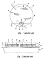
- Figure 1 illustrates a top view of a wafer 30 being planarized by a conventional polishing process in accordance with the prior art.
- a polishing pad 10 is generally rotated at approximately 40 rpm in the direction indicated by arrow P, and the wafer 30 is rotated at approximately 10-30 rpm in the direction indicated by arrow R.
- the wafer 30 also translates across the polishing pad 10 while the wafer 30 rotates.
- a slurry 20 is discharged onto the top of the polishing pad 10 through a pipe 21.
- the wafer 30 scrapes the slurry 20 off of the polishing pad 10, and thus the slurry 20 tends to build up in a high zone 22 that extends approximately from an inside point 32 to an outside point 34 along a leading edge 33 around the perimeter of the wafer 30.
- the excess of slurry in the high zone 22 depletes the slurry from the center of the wafer to the trailing edge 35.
- the wafer 30 accordingly experiences a non-uniform, center-to-edge slurry distribution that reduces the uniformity of the surface of the wafer.
- Figure 2 schematically illustrates a cross-section of an SOF wafer 30 being planarized with a conventional CMP method.
- the wafer 30 has a number of features 37 fabricated onto its surface.
- a first dielectric layer 40 is deposited over the features 37 and the wafer 30, and a second dielectric layer 42 is deposited over the first dielectric layer 40.
- the first dielectric layer 40 has a lower polishing rate than that of the second dielectric layer 42 to enhance the planarity of the resulting dielectric layer, as discussed above in the Background of the Invention section.
- the wafer 30 is positioned opposite the polishing pad 10 such that the surface of the second dielectric layer 42 is placed against the slurry 20.
- the high zone 22 of the slurry 20 builds up along the area adjacent to the leading edge 33, but the low zone 24 is substantially void of any slurry 20 from approximately the center of the wafer to the trailing edge 35. Accordingly, both the mechanical and chemical removal of the resulting surface is generally non-uniform because the slurry is not distributed evenly across the whole surface of the wafer.
- Figure 3 illustrates the steps in an embodiment of a method for chemical-mechanical planarization of an SOF semiconductor wafer.
- a wafer is positioned against a liquid solution over a planarizing surface of a polishing pad.
- the liquid solution may be a conventional CMP slurry that mechanically removes material from the wafer with abrasive particles and chemically removes materials with etching and/or oxidizing chemicals.
- the abrasive particles are made from a material selective to silicon oxide, such as CeO 2 .
- the liquid solution may also be a non-abrasive solution without abrasive particles, such as a solution containing ammonium hydroxide as an active agent to selectively remove silicon oxide from an underlayer of silicon nitride.
- a non-abrasive solution such as a solution containing ammonium hydroxide as an active agent to selectively remove silicon oxide from an underlayer of silicon nitride.
- the polishing pad preferably is impregnated with abrasive particles to provide an abrasive polishing surface on the pad.
- the pad and wafer are moved with respect to each other at relatively low velocities to provide a substantially continuous film of liquid solution between the wafer and the pad.
- a 51-61 cm (20-24 inch) diameter pad is rotated at approximately 25-35 rpm, and preferably at approximately 30 rpm.
- the wafer is preferably rotated at approximately 10-30 rpm, and preferably at approximately 15 rpm.
- the relative velocity between the pad and the wafer is controlled to hydroplane the wafer on the liquid solution and provide a substantially continuous film of liquid solution between the wafer and the pad.
- a Rodel IC-1000 perforated pad with standard perforations manufactured by Rodel Corporation of Newark, Delaware, is covered with a Rodel ILD-1300 slurry (also manufactured by Rodel Corporation).
- the pad preferably is rotated at 25-35 rpm, the wafer preferably is rotated at 10-30 rpm, and the down force against the wafer preferably is 34.4 kPa (5 psi).
- the relative velocity between the wafer and the pad is generally low compared to conventional CMP techniques to enhance the selective removal of material from the wafer.
- Low relative velocities reduce the non-selective mechanical removal of wafer material because fewer abrasive particles abrade the surface of the wafer.
- Low relative velocities also enhance the chemically selective removal of material because a more uniform film of the liquid solution covers the surface of the wafer and the temperature at the pad-wafer interface is reduced.
- the temperature of the pad is controlled to further enhance the selective removal of material from the wafer.
- the pad temperature is controlled by maintaining the platen at a temperature of approximately 30-40°C (85°F-105°F), and preferably approximately 31.6-32.7°C (89°F-91°F).
- the platen temperature is significantly lower in the method of the invention. The lower platen temperature reduces the rate at which the chemicals in the slurry react with the material on the wafer to further enhance the selective removal of one layer of material.
- an SOF wafer 30 is shown being planarized in accordance with the method discussed above with respect to Figure 3.
- the pad rotates at approximately 25-35 rpm, and the platen 12 is heated to approximately 29-40°C (85°F-105°F).
- the slurry 20 is selective to the second dielectric layer 42 on the wafer 30 to remove material from the second dielectric layer 42 without significantly removing material from the first dielectric layer 40.
- a minimal amount of material is removed from the exposed portions of the first layer 40 as the wafer 30 is further planarized.
- the method illustrated in Figures 3 and 4 produces a more uniform surface on SOF wafers because it reduces the mechanical abrasion of the wafer and enhances the selective removal of the second dielectric layer 42.
- the invention reduces mechanical removal of material by moving the pad and wafer with respect to each other at a relative velocity that provides a thin, substantially continuous film of liquid solution between the pad and the wafer.
- the invention accordingly enhances the selective removal of the second dielectric layer 42 because the slower pad speed, lower pad-wafer interface temperature, and reduced abrasion allow the slurry chemicals to aggressively remove the second dielectric layer 42 without removing significant amounts of the first dielectric layer 40.
- the method illustrated in Figure 3 produces a wafer with step heights between 200 ⁇ -300 ⁇ .
- the method illustrated in Figures 3 and 4 also produces a more uniformly planar surface on the wafer because the polishing pad surface deteriorates substantially uniformly.
- the substantially continuous film of liquid solution between the pad and the wafer reduces the contact between the pad and wafer.
- the initially exposed two-component areas on the wafer are substantially prevented from abrading localized areas on the pad.
- the spatial differentiations of the polishing rate across the pad therefore, are substantially reduced by the present invention.
- FIGS 5A and 5B illustrate a suitable high-slurry-transport polishing pad 100 that has a body 101 and a number of wells 102 formed into the body 101.
- the upper surface of the body 101 defines a planarizing surface 106, and each of the wells has a hole 104 at the planarizing surface 106.
- the holes 104 each have an open area that, in the case of a circular hole, is determined by the diameter "d" of each of the holes 104.
- the holes 104 are spaced apart from one another in a uniform pattern such that the ratio of the open area of the holes 104 to the surface area of the planarizing surface 106 is substantially constant across the entire pad 100.
- the ratio of the open area of the holes 104 to the surface area 106 in a region 110 is substantially equal to that of another region 112.
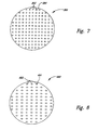
- Figures 6-8 illustrate alternative embodiments of high-slurry-transport polishing pads.
- Figure 6 illustrates a polishing pad 200 with wells 102 that are formed in a uniform pattern in which the wells 102 are spaced an equal distance from one another across the surface area of the pad 200.
- Figure 7 illustrates another polishing pad 300 with wells 302 that have rectangular holes 304
- Figure 8 illustrates another pad 400 with wells 402 that have elliptical holes 404.
- a pad with circular holes such as the holes 104 of pads 100 and 200 shown in Figures 5A and 5B, is used in the method of the invention.
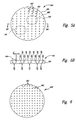
- Figure 9A schematically shows an SOF wafer 30 being polished by a pad 100 at a first point in time.
- the pad 100 rotates at a rate between 25 and 35 rpm in a direction P, and the wafer 30 rotates at a rate between 10 and 30 rpm in a direction R, to cause the wafer 30 to ride on a substantially continuous film of slurry.
- the pad 100 generally has a much larger radius than the wafer 30, and thus the pad 100 has a much higher linear velocity than that of the wafer 30.
- the slurry 20 fills the wells 102 before the wells 102 pass under the wafer 30, as shown by wells 102(j) through 102(m).
- the difference in velocity between the pad 100 and the wafer 30 creates a low pressure region along the planarizing surface 106 of the pad that draws the slurry 20 out of the wells 102.
- Wells 102(j) and 102(k) which have just passed by the leading edge 33 of the wafer, are thus still full of slurry 20.
- well 102(h) has an empty space 109(h) bounded by the lower level 108 of the slurry 20 because the low pressure region above the planarizing surface 106 has drawn some of the slurry out of well 102(h).
- Figure 9B shows the pad 100 at a subsequent point in time after which well 102(l) has moved from the leading edge 33 to the trailing edge 35.
- well 102(a) the slurry 20 in well 102(l) has been drawn out of the well into the space between the second dielectric layer 42 and the planarizing surface 106.
- the size of the holes 104 are small enough to create a sufficiently large pressure differential at the planarizing surface 106 in order to continuously draw the slurry 20 out of the wells 102.
- circular holes have a diameter between 1 and 3 mm, but other holes sizes are within the scope of the invention according to the velocity difference between the pad 100 and the wafer 30.
- the depth and width of the wells 102 are large enough to hold a sufficient volume of slurry 20 so that the wells are not completely drained by the time they pass the trailing edge 35 of the wafer 30.
- a high-slurry-transport pad such as the pad 100 shown in Figures 9A and 9B, is especially useful in the method of the invention for planarizing SOF wafers with a slurry that is selective to-the second dielectric layer 42.
- the pad 100 enhances the ability to provide a substantially continuous film of slurry between the wafer 30 and the pad 100.
- a high-slurry transport pad further reduces removal of material from the initially exposed regions of the first dielectric layer 40.
- the present invention significantly enhances the uniformity of the planarized surface because it relies on the selectivity of the slurry, and enhances such selectivity by maximizing chemical planarization while minimizing mechanical planarization.
- the selectivity of the slurry solution is enhanced by the following aspects of the method of the invention: (1) moving the wafer and the pad with respect to each other at a low relative velocity that provides a substantially continuous film of slurry between the pad and wafer and reduces the temperature at the pad-wafer interface; and (2) using a relatively low platen temperature to reduce the temperature at the pad-wafer interface.
- a high-slurry-transport pad is preferably used in the method of the invention. Accordingly, the present invention substantially prevents removal of material from the initially exposed regions of the first dielectric layer, while still allowing removal of material from the second dielectric layer.
Abstract
Description
Claims (13)
- A chemical-mechanical planarization method to selectively remove an upper layer from a stop-on-feature layer of a stop-on-feature semiconductor wafer (30), comprising:positioning the wafer (30) against a layer (20) of liquid solution on a planarizing suface (106) of a polishing pad (10; 100; 200; 300, 400), the planarizing surface (106) having a surface area and the polishing pad having a plurality of wells (102; 302; 402) for holding the liquid solution, each well having an opening (104', 304; 404) that defines an open area on the planarizing surface, the openings being spaced apart from each other to provide a constant ration between the open area of the openings and the area of the planarizing surface across the pad;moving at least one of the pad or the wafer (30) with respect to the other at a relatively low velocity to provide a substantially continuous film of liquid solution between the wafer (30) and the polishing pad; andcontrolling the temperature of a platen upon which the pad (10; 100; 200; 300; 400) is positioned to maintain a desired temperature of the liquid solution and to stiffen the polishing pad.
- The method of claim 1 wherein the controlling step comprises maintaining the platen at a temperature between approximately 29°C and 40°C (85°F and 105°F).
- The method of claim 1 wherein the controlling step comprises maintaining the platen at a temperature of approximately 31.6°C - 32.7°C (89°F-91°F).
- The method of claim 1 wherein the liquid solution comprises a polishing slurry containing abrasive particles (28).
- The method of claim 1 wherein the liquid solution comprises a non-abrasive polishing solution without abrasive particles (28).
- The method of claim 5 wherein the polishing pad comprises a matrix material impregnated with abrasive particles.
- The method of claim 2 wherein the moving step coprises rotating the wafer at 10-35 rpm.
- The method of claim 1 wherein the upper layer is made from doped silicon oxide and the stop-on-feature layer is made from silicon nitride.
- The method of any of claims 1 to 8, wherein the planarizing surface of the polishing pad is configured to enhance fluid transport between the wafer (30) and the pad (100, 200, 300, 400),
and wherein a desired temperature of the liquid solution is maintained at which the solution is selective to a layer of material on the wafer and to stiffen the pad. - The method of claim 9, further comprising the step of selecting a slurry solutuion that selectively removes material from one layer of a stop-on-feature layer design.
- The method of claim 1 wherein the openings are sized to create a low pressure region in the slurry adjacent to the wells as a wafer is passed over the wells, and wherein moving at least one of the wafer or the pad with respect to the other comprises sliding the wafer across the pad at a relative velocity at which a portion of the slurry solution in the wells is drawn out of the wells into contact with the wafer to distribute a substantially constant amount of slurry solution across the surface of the wafer.
- The method of claim 1 wherein the liquid solution contains ammonium hydroxide.
- The method of claim 1 wherein the polishing pad is impregnated with abrasive particles.
Applications Claiming Priority (3)
| Application Number | Priority Date | Filing Date | Title |
|---|---|---|---|
| US651896 | 1996-05-21 | ||
| US08/651,896 US5893754A (en) | 1996-05-21 | 1996-05-21 | Method for chemical-mechanical planarization of stop-on-feature semiconductor wafers |
| PCT/US1997/008786 WO1997044160A1 (en) | 1996-05-21 | 1997-05-21 | Method for chemical-mechanical planarization of stop-on-feature semiconductor wafers |
Publications (2)
| Publication Number | Publication Date |
|---|---|
| EP0907460A1 EP0907460A1 (en) | 1999-04-14 |
| EP0907460B1 true EP0907460B1 (en) | 2003-03-26 |
Family
ID=24614677
Family Applications (1)
| Application Number | Title | Priority Date | Filing Date |
|---|---|---|---|
| EP97927723A Expired - Lifetime EP0907460B1 (en) | 1996-05-21 | 1997-05-21 | Method for chemical-mechanical planarization of stop-on-feature semiconductor wafers |
Country Status (8)
| Country | Link |
|---|---|
| US (2) | US5893754A (en) |
| EP (1) | EP0907460B1 (en) |
| JP (1) | JP4219984B2 (en) |
| KR (1) | KR100412165B1 (en) |
| AT (1) | ATE235347T1 (en) |
| AU (1) | AU3211697A (en) |
| DE (1) | DE69720212T2 (en) |
| WO (1) | WO1997044160A1 (en) |
Families Citing this family (62)
| Publication number | Priority date | Publication date | Assignee | Title |
|---|---|---|---|---|
| US6075606A (en) | 1996-02-16 | 2000-06-13 | Doan; Trung T. | Endpoint detector and method for measuring a change in wafer thickness in chemical-mechanical polishing of semiconductor wafers and other microelectronic substrates |
| US5871392A (en) * | 1996-06-13 | 1999-02-16 | Micron Technology, Inc. | Under-pad for chemical-mechanical planarization of semiconductor wafers |
| JP3144635B2 (en) * | 1998-10-13 | 2001-03-12 | 日本電気株式会社 | Method for manufacturing semiconductor device |
| US6407000B1 (en) | 1999-04-09 | 2002-06-18 | Micron Technology, Inc. | Method and apparatuses for making and using bi-modal abrasive slurries for mechanical and chemical-mechanical planarization of microelectronic-device substrate assemblies |
| US6599836B1 (en) * | 1999-04-09 | 2003-07-29 | Micron Technology, Inc. | Planarizing solutions, planarizing machines and methods for mechanical or chemical-mechanical planarization of microelectronic-device substrate assemblies |
| US20050118839A1 (en) * | 1999-04-23 | 2005-06-02 | Industrial Technology Research Institute | Chemical mechanical polish process control method using thermal imaging of polishing pad |
| JP2001018169A (en) | 1999-07-07 | 2001-01-23 | Ebara Corp | Polishing device |
| US6383934B1 (en) | 1999-09-02 | 2002-05-07 | Micron Technology, Inc. | Method and apparatus for chemical-mechanical planarization of microelectronic substrates with selected planarizing liquids |
| US6364749B1 (en) | 1999-09-02 | 2002-04-02 | Micron Technology, Inc. | CMP polishing pad with hydrophilic surfaces for enhanced wetting |
| US6306768B1 (en) | 1999-11-17 | 2001-10-23 | Micron Technology, Inc. | Method for planarizing microelectronic substrates having apertures |
| US6498101B1 (en) | 2000-02-28 | 2002-12-24 | Micron Technology, Inc. | Planarizing pads, planarizing machines and methods for making and using planarizing pads in mechanical and chemical-mechanical planarization of microelectronic device substrate assemblies |
| US6402591B1 (en) * | 2000-03-31 | 2002-06-11 | Lam Research Corporation | Planarization system for chemical-mechanical polishing |
| US6313038B1 (en) | 2000-04-26 | 2001-11-06 | Micron Technology, Inc. | Method and apparatus for controlling chemical interactions during planarization of microelectronic substrates |
| US6387289B1 (en) * | 2000-05-04 | 2002-05-14 | Micron Technology, Inc. | Planarizing machines and methods for mechanical and/or chemical-mechanical planarization of microelectronic-device substrate assemblies |
| US6612901B1 (en) | 2000-06-07 | 2003-09-02 | Micron Technology, Inc. | Apparatus for in-situ optical endpointing of web-format planarizing machines in mechanical or chemical-mechanical planarization of microelectronic-device substrate assemblies |
| US6520834B1 (en) | 2000-08-09 | 2003-02-18 | Micron Technology, Inc. | Methods and apparatuses for analyzing and controlling performance parameters in mechanical and chemical-mechanical planarization of microelectronic substrates |
| US6736869B1 (en) * | 2000-08-28 | 2004-05-18 | Micron Technology, Inc. | Method for forming a planarizing pad for planarization of microelectronic substrates |
| US6838382B1 (en) * | 2000-08-28 | 2005-01-04 | Micron Technology, Inc. | Method and apparatus for forming a planarizing pad having a film and texture elements for planarization of microelectronic substrates |
| US6592443B1 (en) | 2000-08-30 | 2003-07-15 | Micron Technology, Inc. | Method and apparatus for forming and using planarizing pads for mechanical and chemical-mechanical planarization of microelectronic substrates |
| US6609947B1 (en) * | 2000-08-30 | 2003-08-26 | Micron Technology, Inc. | Planarizing machines and control systems for mechanical and/or chemical-mechanical planarization of micro electronic substrates |
| US6652764B1 (en) | 2000-08-31 | 2003-11-25 | Micron Technology, Inc. | Methods and apparatuses for making and using planarizing pads for mechanical and chemical-mechanical planarization of microelectronic substrates |
| US6623329B1 (en) | 2000-08-31 | 2003-09-23 | Micron Technology, Inc. | Method and apparatus for supporting a microelectronic substrate relative to a planarization pad |
| US6679769B2 (en) | 2000-09-19 | 2004-01-20 | Rodel Holdings, Inc | Polishing pad having an advantageous micro-texture and methods relating thereto |
| US6935013B1 (en) * | 2000-11-10 | 2005-08-30 | Hitachi Global Storage Technologies Netherlands B.V. | Apparatus and method for precise lapping of recessed and protruding elements in a workpiece |
| US6811470B2 (en) | 2001-07-16 | 2004-11-02 | Applied Materials Inc. | Methods and compositions for chemical mechanical polishing shallow trench isolation substrates |
| US6722943B2 (en) * | 2001-08-24 | 2004-04-20 | Micron Technology, Inc. | Planarizing machines and methods for dispensing planarizing solutions in the processing of microelectronic workpieces |
| US6866566B2 (en) * | 2001-08-24 | 2005-03-15 | Micron Technology, Inc. | Apparatus and method for conditioning a contact surface of a processing pad used in processing microelectronic workpieces |
| US6677239B2 (en) | 2001-08-24 | 2004-01-13 | Applied Materials Inc. | Methods and compositions for chemical mechanical polishing |
| US6666749B2 (en) | 2001-08-30 | 2003-12-23 | Micron Technology, Inc. | Apparatus and method for enhanced processing of microelectronic workpieces |
| US7199056B2 (en) * | 2002-02-08 | 2007-04-03 | Applied Materials, Inc. | Low cost and low dishing slurry for polysilicon CMP |
| US7131889B1 (en) * | 2002-03-04 | 2006-11-07 | Micron Technology, Inc. | Method for planarizing microelectronic workpieces |
| US6541397B1 (en) * | 2002-03-29 | 2003-04-01 | Applied Materials, Inc. | Removable amorphous carbon CMP stop |
| US6869335B2 (en) | 2002-07-08 | 2005-03-22 | Micron Technology, Inc. | Retaining rings, planarizing apparatuses including retaining rings, and methods for planarizing micro-device workpieces |
| US7341502B2 (en) * | 2002-07-18 | 2008-03-11 | Micron Technology, Inc. | Methods and systems for planarizing workpieces, e.g., microelectronic workpieces |
| US7169014B2 (en) * | 2002-07-18 | 2007-01-30 | Micron Technology, Inc. | Apparatuses for controlling the temperature of polishing pads used in planarizing micro-device workpieces |
| US6860798B2 (en) * | 2002-08-08 | 2005-03-01 | Micron Technology, Inc. | Carrier assemblies, planarizing apparatuses including carrier assemblies, and methods for planarizing micro-device workpieces |
| US7094695B2 (en) * | 2002-08-21 | 2006-08-22 | Micron Technology, Inc. | Apparatus and method for conditioning a polishing pad used for mechanical and/or chemical-mechanical planarization |
| US7004817B2 (en) | 2002-08-23 | 2006-02-28 | Micron Technology, Inc. | Carrier assemblies, planarizing apparatuses including carrier assemblies, and methods for planarizing micro-device workpieces |
| US7011566B2 (en) * | 2002-08-26 | 2006-03-14 | Micron Technology, Inc. | Methods and systems for conditioning planarizing pads used in planarizing substrates |
| US6841991B2 (en) * | 2002-08-29 | 2005-01-11 | Micron Technology, Inc. | Planarity diagnostic system, E.G., for microelectronic component test systems |
| US7008299B2 (en) * | 2002-08-29 | 2006-03-07 | Micron Technology, Inc. | Apparatus and method for mechanical and/or chemical-mechanical planarization of micro-device workpieces |
| US7063597B2 (en) | 2002-10-25 | 2006-06-20 | Applied Materials | Polishing processes for shallow trench isolation substrates |
| US7074114B2 (en) | 2003-01-16 | 2006-07-11 | Micron Technology, Inc. | Carrier assemblies, polishing machines including carrier assemblies, and methods for polishing micro-device workpieces |
| US6884152B2 (en) | 2003-02-11 | 2005-04-26 | Micron Technology, Inc. | Apparatuses and methods for conditioning polishing pads used in polishing micro-device workpieces |
| US6872132B2 (en) * | 2003-03-03 | 2005-03-29 | Micron Technology, Inc. | Systems and methods for monitoring characteristics of a polishing pad used in polishing micro-device workpieces |
| US6935929B2 (en) | 2003-04-28 | 2005-08-30 | Micron Technology, Inc. | Polishing machines including under-pads and methods for mechanical and/or chemical-mechanical polishing of microfeature workpieces |
| US7131891B2 (en) * | 2003-04-28 | 2006-11-07 | Micron Technology, Inc. | Systems and methods for mechanical and/or chemical-mechanical polishing of microfeature workpieces |
| US7763548B2 (en) * | 2003-08-06 | 2010-07-27 | Micron Technology, Inc. | Microfeature workpiece processing system for, e.g., semiconductor wafer analysis |
| US7030603B2 (en) * | 2003-08-21 | 2006-04-18 | Micron Technology, Inc. | Apparatuses and methods for monitoring rotation of a conductive microfeature workpiece |
| US6939211B2 (en) * | 2003-10-09 | 2005-09-06 | Micron Technology, Inc. | Planarizing solutions including abrasive elements, and methods for manufacturing and using such planarizing solutions |
| US7086927B2 (en) * | 2004-03-09 | 2006-08-08 | Micron Technology, Inc. | Methods and systems for planarizing workpieces, e.g., microelectronic workpieces |
| US7066792B2 (en) * | 2004-08-06 | 2006-06-27 | Micron Technology, Inc. | Shaped polishing pads for beveling microfeature workpiece edges, and associate system and methods |
| US7033253B2 (en) * | 2004-08-12 | 2006-04-25 | Micron Technology, Inc. | Polishing pad conditioners having abrasives and brush elements, and associated systems and methods |
| US20060088976A1 (en) * | 2004-10-22 | 2006-04-27 | Applied Materials, Inc. | Methods and compositions for chemical mechanical polishing substrates |
| US7264539B2 (en) * | 2005-07-13 | 2007-09-04 | Micron Technology, Inc. | Systems and methods for removing microfeature workpiece surface defects |
| US7438626B2 (en) * | 2005-08-31 | 2008-10-21 | Micron Technology, Inc. | Apparatus and method for removing material from microfeature workpieces |
| US7326105B2 (en) * | 2005-08-31 | 2008-02-05 | Micron Technology, Inc. | Retaining rings, and associated planarizing apparatuses, and related methods for planarizing micro-device workpieces |
| US7294049B2 (en) * | 2005-09-01 | 2007-11-13 | Micron Technology, Inc. | Method and apparatus for removing material from microfeature workpieces |
| TW200736001A (en) * | 2006-03-27 | 2007-10-01 | Toshiba Kk | Polishing pad, method of polishing and polishing apparatus |
| US7754612B2 (en) * | 2007-03-14 | 2010-07-13 | Micron Technology, Inc. | Methods and apparatuses for removing polysilicon from semiconductor workpieces |
| KR20190035241A (en) * | 2017-09-26 | 2019-04-03 | 삼성전자주식회사 | Method of controlling a temperature of a chemical mechanical polishing (cmp) process, temperature control unit for performing the method, and cmp apparatus including the temperature control unit |
| CN117733662B (en) * | 2024-02-19 | 2024-04-16 | 南方科技大学 | Diamond polishing method based on plasma etching and modification effects |
Citations (1)
| Publication number | Priority date | Publication date | Assignee | Title |
|---|---|---|---|---|
| US5578362A (en) * | 1992-08-19 | 1996-11-26 | Rodel, Inc. | Polymeric polishing pad containing hollow polymeric microelements |
Family Cites Families (10)
| Publication number | Priority date | Publication date | Assignee | Title |
|---|---|---|---|---|
| US4910155A (en) * | 1988-10-28 | 1990-03-20 | International Business Machines Corporation | Wafer flood polishing |
| US5020283A (en) * | 1990-01-22 | 1991-06-04 | Micron Technology, Inc. | Polishing pad with uniform abrasion |
| US5234867A (en) * | 1992-05-27 | 1993-08-10 | Micron Technology, Inc. | Method for planarizing semiconductor wafers with a non-circular polishing pad |
| US5104828A (en) * | 1990-03-01 | 1992-04-14 | Intel Corporation | Method of planarizing a dielectric formed over a semiconductor substrate |
| US5036015A (en) * | 1990-09-24 | 1991-07-30 | Micron Technology, Inc. | Method of endpoint detection during chemical/mechanical planarization of semiconductor wafers |
| US5069002A (en) * | 1991-04-17 | 1991-12-03 | Micron Technology, Inc. | Apparatus for endpoint detection during mechanical planarization of semiconductor wafers |
| US5232875A (en) * | 1992-10-15 | 1993-08-03 | Micron Technology, Inc. | Method and apparatus for improving planarity of chemical-mechanical planarization operations |
| US5300155A (en) * | 1992-12-23 | 1994-04-05 | Micron Semiconductor, Inc. | IC chemical mechanical planarization process incorporating slurry temperature control |
| US5575706A (en) * | 1996-01-11 | 1996-11-19 | Taiwan Semiconductor Manufacturing Company Ltd. | Chemical/mechanical planarization (CMP) apparatus and polish method |
| US5647952A (en) * | 1996-04-01 | 1997-07-15 | Industrial Technology Research Institute | Chemical/mechanical polish (CMP) endpoint method |
-
1996
- 1996-05-21 US US08/651,896 patent/US5893754A/en not_active Expired - Lifetime
-
1997
- 1997-05-21 WO PCT/US1997/008786 patent/WO1997044160A1/en active IP Right Grant
- 1997-05-21 DE DE69720212T patent/DE69720212T2/en not_active Expired - Lifetime
- 1997-05-21 JP JP54277597A patent/JP4219984B2/en not_active Expired - Fee Related
- 1997-05-21 KR KR10-1998-0709557A patent/KR100412165B1/en not_active IP Right Cessation
- 1997-05-21 AT AT97927723T patent/ATE235347T1/en not_active IP Right Cessation
- 1997-05-21 EP EP97927723A patent/EP0907460B1/en not_active Expired - Lifetime
- 1997-05-21 AU AU32116/97A patent/AU3211697A/en not_active Abandoned
-
1999
- 1999-04-07 US US09/287,953 patent/US5981396A/en not_active Expired - Lifetime
Patent Citations (1)
| Publication number | Priority date | Publication date | Assignee | Title |
|---|---|---|---|---|
| US5578362A (en) * | 1992-08-19 | 1996-11-26 | Rodel, Inc. | Polymeric polishing pad containing hollow polymeric microelements |
Also Published As
| Publication number | Publication date |
|---|---|
| JP2000511355A (en) | 2000-08-29 |
| EP0907460A1 (en) | 1999-04-14 |
| AU3211697A (en) | 1997-12-09 |
| KR100412165B1 (en) | 2004-04-28 |
| US5981396A (en) | 1999-11-09 |
| DE69720212D1 (en) | 2003-04-30 |
| JP4219984B2 (en) | 2009-02-04 |
| US5893754A (en) | 1999-04-13 |
| DE69720212T2 (en) | 2003-12-18 |
| WO1997044160A1 (en) | 1997-11-27 |
| KR20000015996A (en) | 2000-03-25 |
| ATE235347T1 (en) | 2003-04-15 |
Similar Documents
| Publication | Publication Date | Title |
|---|---|---|
| EP0907460B1 (en) | Method for chemical-mechanical planarization of stop-on-feature semiconductor wafers | |
| US8133096B2 (en) | Multi-phase polishing pad | |
| US6331135B1 (en) | Method and apparatus for mechanical and chemical-mechanical planarization of microelectronic substrates with metal compound abrasives | |
| US6238271B1 (en) | Methods and apparatus for improved polishing of workpieces | |
| US5855804A (en) | Method and apparatus for stopping mechanical and chemical-mechanical planarization of substrates at desired endpoints | |
| US6039633A (en) | Method and apparatus for mechanical and chemical-mechanical planarization of microelectronic-device substrate assemblies | |
| US6890591B2 (en) | Polishing pads and planarizing machines for mechanical or chemical-mechanical planarization of microelectronic-device substrate assemblies, and methods for making and using such pads and machines | |
| KR102363154B1 (en) | Debris-removal groove for cmp polishing pad | |
| US6423640B1 (en) | Headless CMP process for oxide planarization | |
| US6955587B2 (en) | Grooved polishing pad and method | |
| EP0622155A1 (en) | Polishing pad and a method of polishing a semiconductor substrate | |
| KR100394572B1 (en) | multi characterized CMP pad structure and method for fabricating same | |
| US7070480B2 (en) | Method and apparatus for polishing substrates | |
| EP0808231B1 (en) | Chemical-mechanical polishing using curved carriers | |
| US6899612B2 (en) | Polishing pad apparatus and methods | |
| US6422929B1 (en) | Polishing pad for a linear polisher and method for forming | |
| JP2000042903A (en) | Lapping method |
Legal Events
| Date | Code | Title | Description |
|---|---|---|---|
| PUAI | Public reference made under article 153(3) epc to a published international application that has entered the european phase |
Free format text: ORIGINAL CODE: 0009012 |
|
| 17P | Request for examination filed |
Effective date: 19981217 |
|
| AK | Designated contracting states |
Kind code of ref document: A1 Designated state(s): AT BE CH DE DK ES FI FR GB GR IE IT LI LU MC NL PT SE |
|
| 17Q | First examination report despatched |
Effective date: 20010328 |
|
| GRAG | Despatch of communication of intention to grant |
Free format text: ORIGINAL CODE: EPIDOS AGRA |
|
| GRAG | Despatch of communication of intention to grant |
Free format text: ORIGINAL CODE: EPIDOS AGRA |
|
| GRAG | Despatch of communication of intention to grant |
Free format text: ORIGINAL CODE: EPIDOS AGRA |
|
| GRAH | Despatch of communication of intention to grant a patent |
Free format text: ORIGINAL CODE: EPIDOS IGRA |
|
| GRAH | Despatch of communication of intention to grant a patent |
Free format text: ORIGINAL CODE: EPIDOS IGRA |
|
| GRAA | (expected) grant |
Free format text: ORIGINAL CODE: 0009210 |
|
| AK | Designated contracting states |
Designated state(s): AT BE CH DE DK ES FI FR GB GR IE IT LI LU MC NL PT SE |
|
| PG25 | Lapsed in a contracting state [announced via postgrant information from national office to epo] |
Ref country code: NL Free format text: LAPSE BECAUSE OF FAILURE TO SUBMIT A TRANSLATION OF THE DESCRIPTION OR TO PAY THE FEE WITHIN THE PRESCRIBED TIME-LIMIT Effective date: 20030326 Ref country code: LI Free format text: LAPSE BECAUSE OF FAILURE TO SUBMIT A TRANSLATION OF THE DESCRIPTION OR TO PAY THE FEE WITHIN THE PRESCRIBED TIME-LIMIT Effective date: 20030326 Ref country code: GR Free format text: LAPSE BECAUSE OF FAILURE TO SUBMIT A TRANSLATION OF THE DESCRIPTION OR TO PAY THE FEE WITHIN THE PRESCRIBED TIME-LIMIT Effective date: 20030326 Ref country code: FI Free format text: LAPSE BECAUSE OF FAILURE TO SUBMIT A TRANSLATION OF THE DESCRIPTION OR TO PAY THE FEE WITHIN THE PRESCRIBED TIME-LIMIT Effective date: 20030326 Ref country code: CH Free format text: LAPSE BECAUSE OF FAILURE TO SUBMIT A TRANSLATION OF THE DESCRIPTION OR TO PAY THE FEE WITHIN THE PRESCRIBED TIME-LIMIT Effective date: 20030326 Ref country code: BE Free format text: LAPSE BECAUSE OF FAILURE TO SUBMIT A TRANSLATION OF THE DESCRIPTION OR TO PAY THE FEE WITHIN THE PRESCRIBED TIME-LIMIT Effective date: 20030326 Ref country code: AT Free format text: LAPSE BECAUSE OF FAILURE TO SUBMIT A TRANSLATION OF THE DESCRIPTION OR TO PAY THE FEE WITHIN THE PRESCRIBED TIME-LIMIT Effective date: 20030326 |
|
| REG | Reference to a national code |
Ref country code: GB Ref legal event code: FG4D |
|
| REG | Reference to a national code |
Ref country code: CH Ref legal event code: EP |
|
| REF | Corresponds to: |
Ref document number: 69720212 Country of ref document: DE Date of ref document: 20030430 Kind code of ref document: P |
|
| REG | Reference to a national code |
Ref country code: IE Ref legal event code: FG4D |
|
| PG25 | Lapsed in a contracting state [announced via postgrant information from national office to epo] |
Ref country code: LU Free format text: LAPSE BECAUSE OF NON-PAYMENT OF DUE FEES Effective date: 20030521 Ref country code: IE Free format text: LAPSE BECAUSE OF NON-PAYMENT OF DUE FEES Effective date: 20030521 |
|
| PG25 | Lapsed in a contracting state [announced via postgrant information from national office to epo] |
Ref country code: MC Free format text: LAPSE BECAUSE OF NON-PAYMENT OF DUE FEES Effective date: 20030531 |
|
| PG25 | Lapsed in a contracting state [announced via postgrant information from national office to epo] |
Ref country code: SE Free format text: LAPSE BECAUSE OF FAILURE TO SUBMIT A TRANSLATION OF THE DESCRIPTION OR TO PAY THE FEE WITHIN THE PRESCRIBED TIME-LIMIT Effective date: 20030626 Ref country code: PT Free format text: LAPSE BECAUSE OF FAILURE TO SUBMIT A TRANSLATION OF THE DESCRIPTION OR TO PAY THE FEE WITHIN THE PRESCRIBED TIME-LIMIT Effective date: 20030626 Ref country code: DK Free format text: LAPSE BECAUSE OF FAILURE TO SUBMIT A TRANSLATION OF THE DESCRIPTION OR TO PAY THE FEE WITHIN THE PRESCRIBED TIME-LIMIT Effective date: 20030626 |
|
| NLV1 | Nl: lapsed or annulled due to failure to fulfill the requirements of art. 29p and 29m of the patents act | ||
| ET | Fr: translation filed | ||
| PG25 | Lapsed in a contracting state [announced via postgrant information from national office to epo] |
Ref country code: ES Free format text: LAPSE BECAUSE OF FAILURE TO SUBMIT A TRANSLATION OF THE DESCRIPTION OR TO PAY THE FEE WITHIN THE PRESCRIBED TIME-LIMIT Effective date: 20030930 |
|
| REG | Reference to a national code |
Ref country code: CH Ref legal event code: PL |
|
| PLBE | No opposition filed within time limit |
Free format text: ORIGINAL CODE: 0009261 |
|
| STAA | Information on the status of an ep patent application or granted ep patent |
Free format text: STATUS: NO OPPOSITION FILED WITHIN TIME LIMIT |
|
| REG | Reference to a national code |
Ref country code: IE Ref legal event code: MM4A |
|
| 26N | No opposition filed |
Effective date: 20031230 |
|
| PGFP | Annual fee paid to national office [announced via postgrant information from national office to epo] |
Ref country code: IT Payment date: 20090522 Year of fee payment: 13 |
|
| PG25 | Lapsed in a contracting state [announced via postgrant information from national office to epo] |
Ref country code: IT Free format text: LAPSE BECAUSE OF NON-PAYMENT OF DUE FEES Effective date: 20100521 |
|
| PGFP | Annual fee paid to national office [announced via postgrant information from national office to epo] |
Ref country code: GB Payment date: 20140521 Year of fee payment: 18 |
|
| PGFP | Annual fee paid to national office [announced via postgrant information from national office to epo] |
Ref country code: DE Payment date: 20140515 Year of fee payment: 18 |
|
| REG | Reference to a national code |
Ref country code: FR Ref legal event code: PLFP Year of fee payment: 19 |
|
| PGFP | Annual fee paid to national office [announced via postgrant information from national office to epo] |
Ref country code: FR Payment date: 20150508 Year of fee payment: 19 |
|
| REG | Reference to a national code |
Ref country code: DE Ref legal event code: R119 Ref document number: 69720212 Country of ref document: DE |
|
| GBPC | Gb: european patent ceased through non-payment of renewal fee |
Effective date: 20150521 |
|
| PG25 | Lapsed in a contracting state [announced via postgrant information from national office to epo] |
Ref country code: DE Free format text: LAPSE BECAUSE OF NON-PAYMENT OF DUE FEES Effective date: 20151201 Ref country code: GB Free format text: LAPSE BECAUSE OF NON-PAYMENT OF DUE FEES Effective date: 20150521 |
|
| REG | Reference to a national code |
Ref country code: FR Ref legal event code: ST Effective date: 20170131 |
|
| PG25 | Lapsed in a contracting state [announced via postgrant information from national office to epo] |
Ref country code: FR Free format text: LAPSE BECAUSE OF NON-PAYMENT OF DUE FEES Effective date: 20160531 |