EP0917409A1 - Lampe électroluminescente et son procédé de production - Google Patents
Lampe électroluminescente et son procédé de production Download PDFInfo
- Publication number
- EP0917409A1 EP0917409A1 EP97120090A EP97120090A EP0917409A1 EP 0917409 A1 EP0917409 A1 EP 0917409A1 EP 97120090 A EP97120090 A EP 97120090A EP 97120090 A EP97120090 A EP 97120090A EP 0917409 A1 EP0917409 A1 EP 0917409A1
- Authority
- EP
- European Patent Office
- Prior art keywords
- layer
- electroluminescent
- electrode layer
- substrate
- dome
- Prior art date
- Legal status (The legal status is an assumption and is not a legal conclusion. Google has not performed a legal analysis and makes no representation as to the accuracy of the status listed.)
- Granted
Links
Images


Classifications
-
- H—ELECTRICITY
- H05—ELECTRIC TECHNIQUES NOT OTHERWISE PROVIDED FOR
- H05B—ELECTRIC HEATING; ELECTRIC LIGHT SOURCES NOT OTHERWISE PROVIDED FOR; CIRCUIT ARRANGEMENTS FOR ELECTRIC LIGHT SOURCES, IN GENERAL
- H05B33/00—Electroluminescent light sources
- H05B33/12—Light sources with substantially two-dimensional radiating surfaces
-
- H—ELECTRICITY
- H01—ELECTRIC ELEMENTS
- H01H—ELECTRIC SWITCHES; RELAYS; SELECTORS; EMERGENCY PROTECTIVE DEVICES
- H01H13/00—Switches having rectilinearly-movable operating part or parts adapted for pushing or pulling in one direction only, e.g. push-button switch
- H01H13/70—Switches having rectilinearly-movable operating part or parts adapted for pushing or pulling in one direction only, e.g. push-button switch having a plurality of operating members associated with different sets of contacts, e.g. keyboard
- H01H13/702—Switches having rectilinearly-movable operating part or parts adapted for pushing or pulling in one direction only, e.g. push-button switch having a plurality of operating members associated with different sets of contacts, e.g. keyboard with contacts carried by or formed from layers in a multilayer structure, e.g. membrane switches
-
- H—ELECTRICITY
- H05—ELECTRIC TECHNIQUES NOT OTHERWISE PROVIDED FOR
- H05B—ELECTRIC HEATING; ELECTRIC LIGHT SOURCES NOT OTHERWISE PROVIDED FOR; CIRCUIT ARRANGEMENTS FOR ELECTRIC LIGHT SOURCES, IN GENERAL
- H05B33/00—Electroluminescent light sources
-
- H—ELECTRICITY
- H01—ELECTRIC ELEMENTS
- H01H—ELECTRIC SWITCHES; RELAYS; SELECTORS; EMERGENCY PROTECTIVE DEVICES
- H01H2219/00—Legends
- H01H2219/002—Legends replaceable; adaptable
- H01H2219/018—Electroluminescent panel
-
- H—ELECTRICITY
- H01—ELECTRIC ELEMENTS
- H01H—ELECTRIC SWITCHES; RELAYS; SELECTORS; EMERGENCY PROTECTIVE DEVICES
- H01H2219/00—Legends
- H01H2219/028—Printed information
-
- H—ELECTRICITY
- H01—ELECTRIC ELEMENTS
- H01H—ELECTRIC SWITCHES; RELAYS; SELECTORS; EMERGENCY PROTECTIVE DEVICES
- H01H2229/00—Manufacturing
- H01H2229/05—Forming; Half-punching
Definitions
- This invention generally relates to the art of electroluminescent lamps and, particularly, to an electroluminescent lamp particularly adapted for use in a key pad.
- Electroluminescent lamp panels are known in the art.
- an electroluminescent lamp typically includes a base electrode spaced from a transparent electrode for sandwiching an electroluminescent or phosphorescent layer therebetween. Often a dielectric layer also is sandwiched between the two electrodes.
- the base electrode may be a foil layer, such as a thin aluminum foil layer, or the base electrode may be a printed layer of conductive ink.
- Conductive leads extend from the base and transparent electrodes of the lamp. When an AC voltage is applied across the leads, the current induced between the base and transparent electrodes causes the phosphorescent layer to emit light, a phenomenon known as luminescence.
- An electroluminescent lamp essentially is a light emitting capacitor having a dielectric layer between two conductive electrodes, one of which is transparent, and the dielectric layer may be a phosphorescent layer, or there may be a separate dielectric layer.
- the transparent electrode layer typically is made of indium tin oxide ("ITO") or indium oxide. Light is visible through the transparent electrode, and various electroluminescent chemicals are known to provide lights of various colors. Lamp panels can include one or a plurality of individual electroluminescent lamps.
- each key includes a dome-shaped actuator key mounted on top of a spacer on top of a printed circuit board which, in turn, is mounted on top of the layered or laminated electroluminescent lamp.
- the actuator key moves a conductive switch member through a hole in the spacer to close a gap between two circuit traces on the board.
- the circuit board typically is separated from the laminated electroluminescent lamp by still a further insulator.
- the components of the electrical circuit including the printed circuit board substrate, the insulator and the switch member must be light-transmissive to allow light from the subjacent electroluminescent lamp to pass therethrough.
- the present invention is directed to solving these various problems by providing a unique arrangement wherein the components of the electroluminescent lamp are located immediately below a substrate, such as a dome-shaped substrate which can function directly as a switch key.
- An object, therefore, of the invention is to provide a new and improved electroluminescent lamp, particularly such a lamp which is especially applicable for use in an electroluminescent lamp panel or keyboard, as well as a method of fabricating an electroluminescent key.
- the electroluminescent lamp includes a flexible dome-shaped, light transmissive substrate defining a top side and a bottom side thereof.
- An upper light transmissive electrode layer is applied on at least a portion of the bottom side of the dome-shaped substrate.
- An electroluminescent layer is applied below the upper light transmissive electrode layer.
- a lower electrode layer is applied below the electroluminescent layer. Therefore, running electrical current through the upper and lower electrode layers causes the electroluminescent layer to emit light through the upper electrode layer and directly through the flexible dome-shaped substrate. There are no extraneous circuits or circuit boards disposed between the electroluminescent lamp and the dome-shaped substrate or key.
- the flexible dome-shaped substrate is preferably fabricated of polycarbonate, but other soft plastic materials may be suitable.
- a dielectric layer may be disposed between the electroluminescent layer and the lower electrode layer.
- a layer of graphic ink may be applied on the bottom side of the dome-shaped substrate.
- a layer of easily stretchable conductive material may be applied about at least a portion of the upper electrode layer for connecting the upper electrode layer to an electrical circuit.
- a silicone material may be provided under the concave side of the dome-shaped substrate.
- the flexible dome-shaped substrate includes a peripheral side wall and a top wall.
- the peripheral side wall is preferably at an obtuse angle with respect to the top wall.
- the upper electrode layer and the electroluminescent layer are located beneath the top wall of the dome-shaped substrate.
- the flexible dome-shaped substrate is shown to be substantially surrounded by a generally flat substrate separated from the dome-shaped substrate by a peripheral cutout.
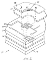
- an electroluminescent switch key generally designated 10
- the switch key includes a switch assembly 12 on top of an electroluminescent lamp 14.
- the key assembly 12 includes a silicone-filled actuator 26 mounted on top of a translucent layer 28 with a dome 28a which, in turn, is mounted on top of a spacer 29 having a recess 29a therein.
- the spacer 29 is mounted on top of a printed circuit board 30 having circuit traces 32a and 32b printed on both sides thereof.
- a translucent insulating layer 34 supports the key assembly 12.
- the electroluminescent lamp is of a typical construction and is applied onto the opposite side of the insulating layer 34 as the key assembly 12.
- a phosphor layer 22 is printed on the electrode layer 24.
- a dielectric layer 20 is applied over the phosphor layer 24.
- a lower electrode layer 18 is applied onto the dielectric layer 20.
- the lower electrode layer may be of conductive ink, such as silver ink, screen printed on the dielectric layer 20.
- the electroluminescent lamp of the invention is incorporated in a key pad, generally designated 44.
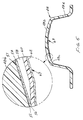
- the key pad includes a generally flat or planar substrate 46, with a generally dome-shaped key or substrate portion, generally designated 48, formed therefrom.
- Key 48 is separated from flat substrate 46 by an annular peripheral cutout 50, except for a web portion 52, for purposes described hereinafter.
- Key 48 has a peripheral side wall 48a and a top wall 48b which gradually merge at a curved bend 48c. It can be seen that the side wall 48a, the top wall 48b and the bend 48c together define a generally convex surface when viewed from above the key 48 and a generally concave surface when viewed from below the key 48.
- the peripheral side wall 48a is preferably at an obtuse angle with respect to the top wall.
- the entire substrate structure, including flat substrate 46 and dome-shaped substrate or key 48 is fabricated of a layer of flexible material, preferably fabricated of polycarbonate.
- dome-shaped key 48 projecting upwardly from flat substrate 46. This would be the normal orientation of the structure as used in a typical keyboard or luminescent lamp panel. Therefore, when using such terms as “upper”, “lower”, “top”, “bottom” and the like is meant to be in reference to this orientation.
- Layer 48b in Figure 4 represents the top wall of dome-shaped substrate or key 48 in an upside-down orientation and prior to forming the substrate into its dome-shaped configuration.
- graphic ink layers 51 and 52 first are printed on polycarbonate substrate 48b. At least graphic layer 51 is light transmitting.
- a light-transmissive electrode layer 54 is sputtered on graphic inks 51 and 52. This electrode layer will become the upper electrode layer in dome-shaped key 48 (Fig. 3).
- This electrode layer may be made of indium tin oxide (“ITO”) material.
- a layer 56 of easily stretchable conductive ink also is printed on graphic layers 51 and 52 for connecting electrode 54 to a supporting electrical circuit, as will be seen in greater detail hereinafter.
- This easily stretchable conductive ink can be silver ink, but carbon ink is preferable for embossing purposes.
- An electroluminescent layer 58 of preferably phosphor is printed on top of electrode layer 54.
- a light-transmissive, dielectric layer 60 is printed over electroluminescent layer 58.
- a second electrode layer 62 is printed over dielectric layer 60.
- This second electrode layer may be of silver ink, and this conductive layer eventually becomes the rear or lower electrode layer beneath dome-shaped substrate of key 48 (Fig. 3).
- FIG. 7 shows the final construction of the electroluminescent lamp and key of the invention. It can be seen that carbon layer 56, which is connected to upper light transmissive electrode layer 54, has a lead portion 56a projecting generally radially outwardly of the substrate structure. Lower electrode layer 62 has a lead portion 62a which also projects radially outwardly of the substrate structure. Web portion 52 of the substrate structure not only supports the dome-shaped substrate or key 48 within the cutout 50 of flat substrate 46, but the web portion also can be used to support leads 56a and 62a. When AC voltage is applied across leads 56a and 62a, current is induced between electrode layers 54 and 62 which causes phosphorescent layer 58 to emit light upwardly through top wall 48b of dome-shaped substrate or key 48. Although it is not shown, a conventional electrical switch can be disposed below the key 48.
- the upper light transmissive electrode 54 is restricted to an area beneath top wall 48b of key 48.
- Stretchable conductive layer 56 then connects the upper electrode across the bend 48c through lead 56a to the source of AC current.
- the upper light transmissive electrode layer 54 is typically fabricated of indium tin oxide which is not as stretchable as layer 56. The more stretchable layer 56 can better withstand the stress and strain forces encountered while being formed into the dome configuration of key 48 than the less flexible indium tin oxide material of upper electrode layer 54.
Priority Applications (6)
| Application Number | Priority Date | Filing Date | Title |
|---|---|---|---|
| DE69732776T DE69732776T2 (de) | 1997-11-17 | 1997-11-17 | Elektrolumineszierende Lampe und Verfahren zur Herstellung |
| EP97120090A EP0917409B1 (fr) | 1997-11-17 | 1997-11-17 | Lampe électroluminescente et son procédé de production |
| US09/190,551 US6246169B1 (en) | 1997-11-17 | 1998-11-12 | Electroluminescent lamp and having a flexible dome-shaped substrate |
| JP34235798A JP3154116B2 (ja) | 1997-11-17 | 1998-11-16 | エレクトロルミネッセント灯およびその製造方法 |
| TW087218937U TW411079U (en) | 1997-11-17 | 1998-11-16 | Electroluminescent lamp |
| CNB98122492XA CN1154400C (zh) | 1997-11-17 | 1998-11-17 | 场致发光灯及其制造方法 |
Applications Claiming Priority (1)
| Application Number | Priority Date | Filing Date | Title |
|---|---|---|---|
| EP97120090A EP0917409B1 (fr) | 1997-11-17 | 1997-11-17 | Lampe électroluminescente et son procédé de production |
Publications (2)
| Publication Number | Publication Date |
|---|---|
| EP0917409A1 true EP0917409A1 (fr) | 1999-05-19 |
| EP0917409B1 EP0917409B1 (fr) | 2005-03-16 |
Family
ID=8227626
Family Applications (1)
| Application Number | Title | Priority Date | Filing Date |
|---|---|---|---|
| EP97120090A Expired - Lifetime EP0917409B1 (fr) | 1997-11-17 | 1997-11-17 | Lampe électroluminescente et son procédé de production |
Country Status (6)
| Country | Link |
|---|---|
| US (1) | US6246169B1 (fr) |
| EP (1) | EP0917409B1 (fr) |
| JP (1) | JP3154116B2 (fr) |
| CN (1) | CN1154400C (fr) |
| DE (1) | DE69732776T2 (fr) |
| TW (1) | TW411079U (fr) |
Cited By (10)
| Publication number | Priority date | Publication date | Assignee | Title |
|---|---|---|---|---|
| WO2001084584A1 (fr) * | 2000-05-01 | 2001-11-08 | Durel Corporation | Ensembles lampes electroluminescentes et leur fabrication |
| WO2002015211A1 (fr) | 2000-08-17 | 2002-02-21 | Nokia Corporation | Dispositif permettant d'intégrer l'éclairage dans le clavier d'appareils électroniques portables |
| WO2002089533A1 (fr) * | 2001-04-25 | 2002-11-07 | Elumina Lighting Technologies, Inc. | Dispositif d'eclairage d'appoint electroluminescent a configuration tridimensionnelle |
| EP1265261A2 (fr) * | 2001-05-22 | 2002-12-11 | Youeal Electronics Co., Ltd. | Clavier pour téléphone mobile comprenant un élément electroluminescent |
| US6527400B2 (en) | 2001-05-01 | 2003-03-04 | Kirkwood Tierney | Electroluminescent supplementary-lighting device having three-dimensional configuration |
| EP1398808A4 (fr) * | 2001-05-25 | 2005-03-16 | Shinetsu Polymer Co | Element pour commutateur a bouton-poussoir et son procede de fabrication |
| GB2412244A (en) * | 2004-02-20 | 2005-09-21 | Pelikon Ltd | Switches |
| EP1889271A1 (fr) * | 2005-06-09 | 2008-02-20 | Oryon Technologies LLC | Commutateur a membrane pour lampe electroluminescente |
| US8344369B2 (en) | 2001-12-28 | 2013-01-01 | Semiconductor Energy Laboratory Co., Ltd. | Vehicle that includes a display panel having a curved surface |
| US10325940B2 (en) | 2001-11-30 | 2019-06-18 | Semiconductor Energy Laboratory Co., Ltd. | Vehicle, display device and manufacturing method for a semiconductor device |
Families Citing this family (42)
| Publication number | Priority date | Publication date | Assignee | Title |
|---|---|---|---|---|
| US7883227B1 (en) * | 1998-08-26 | 2011-02-08 | Andrew Katrinecz | Low power, low cost illuminated keyboards and keypads |
| US20090091478A1 (en) * | 1998-11-13 | 2009-04-09 | Chan Sam E J | Computer keyboard backlighting |
| US7335843B2 (en) * | 1998-11-13 | 2008-02-26 | Firefly International, Inc. | Computer keyboard backlighting |
| US20080212307A1 (en) * | 1998-11-13 | 2008-09-04 | Chan Sam E J | Computer keyboard backlighting |
| JP2002056737A (ja) * | 2000-08-08 | 2002-02-22 | Seiko Precision Inc | 照光式スイッチ |
| JP2002299067A (ja) * | 2001-04-03 | 2002-10-11 | Matsushita Electric Ind Co Ltd | El素子及びこれを用いた照光装置 |
| KR100404102B1 (ko) * | 2001-09-04 | 2003-11-03 | 엘지전자 주식회사 | 휴대단말기의 키패드 백라이팅 장치 |
| NZ532188A (en) | 2001-10-24 | 2006-02-24 | Lumitec Ag | Three-dimensional electroluminescence display which can withstand a high degree of curvature without damage |
| US6926418B2 (en) * | 2002-04-24 | 2005-08-09 | Nokia Corporation | Integrated light-guide and dome-sheet for keyboard illumination |
| US6771021B2 (en) * | 2002-05-28 | 2004-08-03 | Eastman Kodak Company | Lighting apparatus with flexible OLED area illumination light source and fixture |
| JP4302443B2 (ja) * | 2003-06-20 | 2009-07-29 | 信越ポリマー株式会社 | 照光式押釦スイッチ用部材の製造方法 |
| US7128439B2 (en) * | 2003-12-23 | 2006-10-31 | Winsor Corporation | Multi-use planar photoluminescent lamp and method of making such lamp |
| US10575376B2 (en) | 2004-02-25 | 2020-02-25 | Lynk Labs, Inc. | AC light emitting diode and AC LED drive methods and apparatus |
| US10499465B2 (en) | 2004-02-25 | 2019-12-03 | Lynk Labs, Inc. | High frequency multi-voltage and multi-brightness LED lighting devices and systems and methods of using same |
| WO2011143510A1 (fr) | 2010-05-12 | 2011-11-17 | Lynk Labs, Inc. | Système d'éclairage à del |
| US7623118B2 (en) * | 2005-03-14 | 2009-11-24 | Palm, Inc. | Actuation mechanism for use with keyboards on mobile computing devices |
| US7525534B2 (en) | 2005-03-14 | 2009-04-28 | Palm, Inc. | Small form-factor keypad for mobile computing devices |
| US9142369B2 (en) * | 2005-03-14 | 2015-09-22 | Qualcomm Incorporated | Stack assembly for implementing keypads on mobile computing devices |
| US7394030B2 (en) | 2005-06-02 | 2008-07-01 | Palm, Inc. | Small form-factor keyboard using keys with offset peaks and pitch variations |
| CH698138B1 (de) * | 2005-11-09 | 2009-05-29 | Abatek Internat Ag | Integrierter Schalter respektive integrierte Taste. |
| JP2007294320A (ja) * | 2006-04-26 | 2007-11-08 | Sunarrow Ltd | 押釦スイッチ用キートップを製造する方法 |
| US8989822B2 (en) | 2006-09-08 | 2015-03-24 | Qualcomm Incorporated | Keypad assembly for use on a contoured surface of a mobile computing device |
| US7781688B2 (en) * | 2006-10-17 | 2010-08-24 | Legacy Ip Llc | System and method for illuminating a keyboard or keypad input device |
| US11317495B2 (en) | 2007-10-06 | 2022-04-26 | Lynk Labs, Inc. | LED circuits and assemblies |
| US11297705B2 (en) | 2007-10-06 | 2022-04-05 | Lynk Labs, Inc. | Multi-voltage and multi-brightness LED lighting devices and methods of using same |
| US8350728B2 (en) | 2010-04-23 | 2013-01-08 | Hewlett-Packard Development Company, L.P. | Keyboard with integrated and numeric keypad |
| WO2013026053A1 (fr) | 2011-08-18 | 2013-02-21 | Lynk Labs, Inc. | Dispositifs et systèmes ayant des circuits de del à courant alternatif et procédés de commande de ceux-ci |
| WO2013082609A1 (fr) | 2011-12-02 | 2013-06-06 | Lynk Labs, Inc. | Dispositifs d'éclairage par del à faible distorsion harmonique totale (dht) à commande de température de couleur et leurs systèmes et procédés de pilotage |
| TW201421518A (zh) * | 2012-11-21 | 2014-06-01 | Primax Electronics Ltd | 發光鍵盤 |
| KR20150120376A (ko) | 2013-02-20 | 2015-10-27 | 가부시키가이샤 한도오따이 에네루기 켄큐쇼 | 박리 방법, 반도체 장치, 및 박리 장치 |
| CN105793957B (zh) | 2013-12-12 | 2019-05-03 | 株式会社半导体能源研究所 | 剥离方法及剥离装置 |
| US10357582B1 (en) | 2015-07-30 | 2019-07-23 | Vital Vio, Inc. | Disinfecting lighting device |
| US10918747B2 (en) | 2015-07-30 | 2021-02-16 | Vital Vio, Inc. | Disinfecting lighting device |
| US9927097B2 (en) | 2015-07-30 | 2018-03-27 | Vital Vio Inc. | Single diode disinfection |
| US11079077B2 (en) | 2017-08-31 | 2021-08-03 | Lynk Labs, Inc. | LED lighting system and installation methods |
| US10835627B2 (en) | 2017-12-01 | 2020-11-17 | Vital Vio, Inc. | Devices using flexible light emitting layer for creating disinfecting illuminated surface, and related method |
| US10309614B1 (en) | 2017-12-05 | 2019-06-04 | Vital Vivo, Inc. | Light directing element |
| US10413626B1 (en) | 2018-03-29 | 2019-09-17 | Vital Vio, Inc. | Multiple light emitter for inactivating microorganisms |
| US11639897B2 (en) | 2019-03-29 | 2023-05-02 | Vyv, Inc. | Contamination load sensing device |
| US11541135B2 (en) | 2019-06-28 | 2023-01-03 | Vyv, Inc. | Multiple band visible light disinfection |
| US11369704B2 (en) | 2019-08-15 | 2022-06-28 | Vyv, Inc. | Devices configured to disinfect interiors |
| US11878084B2 (en) | 2019-09-20 | 2024-01-23 | Vyv, Inc. | Disinfecting light emitting subcomponent |
Citations (2)
| Publication number | Priority date | Publication date | Assignee | Title |
|---|---|---|---|---|
| WO1994014180A1 (fr) * | 1992-12-16 | 1994-06-23 | Durel Corporation | Dispositifs a lampes electroluminescentes et leur fabrication |
| EP0818793A1 (fr) * | 1995-03-30 | 1998-01-14 | Matsushita Electric Industrial Co., Ltd. | Membrane en feuille electroluminescente et commutateur comprenant cette derniere |
Family Cites Families (34)
| Publication number | Priority date | Publication date | Assignee | Title |
|---|---|---|---|---|
| US2714683A (en) | 1951-12-19 | 1955-08-02 | Gen Electric | Electroluminescent bulb |
| US2900545A (en) | 1953-07-21 | 1959-08-18 | Sylvania Electric Prod | Curved electroluminescent lamp |
| US2919366A (en) | 1957-10-23 | 1959-12-29 | Thorn Electrical Ind Ltd | Electro-luminescent devices |
| US2981858A (en) | 1959-07-21 | 1961-04-25 | Ibm | Electroluminescent decals |
| US3074816A (en) | 1960-10-28 | 1963-01-22 | Westinghouse Electric Corp | Light-transmitting, electrically conducting element |
| US3144643A (en) | 1960-12-10 | 1964-08-11 | Gasaccumulator Svenska Ab | Push-button illuminating device |
| US3226272A (en) | 1961-09-13 | 1965-12-28 | Gen Electric | Electroluminescent lamp manufacture |
| CA1019248A (fr) | 1974-04-01 | 1977-10-18 | Mohabatullah Sobhani | Commutateur a diaphragme elastomerique |
| US4060703A (en) | 1976-11-10 | 1977-11-29 | Everett Jr Seth Leroy | Keyboard switch assembly with tactile feedback having illuminated laminated layers including opaque or transparent conductive layer |
| JPS5686723U (fr) | 1979-12-07 | 1981-07-11 | ||
| JPS5696416A (en) | 1979-12-28 | 1981-08-04 | Alps Electric Co Ltd | Keyboard switch with el display and method of manufacturing same |
| US4320268A (en) | 1980-02-19 | 1982-03-16 | General Electric Company | Illuminated keyboard for electronic devices and the like |
| US4532395A (en) | 1983-09-20 | 1985-07-30 | Timex Corporation | Electroluminescent flexible touch switch panel |
| US4598181A (en) | 1984-11-13 | 1986-07-01 | Gte Communication Systems Corp. | Laminate switch assembly having improved tactile feel and improved reliability of operation |
| DE3511496A1 (de) | 1985-03-29 | 1986-10-09 | Telefunken electronic GmbH, 7100 Heilbronn | Tastschalteinrichtung mit einer durchsichtigen abdeckfolie |
| JPS6237137A (ja) | 1985-08-12 | 1987-02-18 | Sumitomo Electric Ind Ltd | 繊維強化プラスチツクス製リムの製造方法 |
| US4683360A (en) | 1986-05-09 | 1987-07-28 | W. H. Brady Co. | Membrane switch combined with electroluminescent lamp panel |
| US4811175A (en) | 1986-07-09 | 1989-03-07 | Desmet Gregory L | Illuminated switch |
| JPS63199421A (ja) | 1987-02-16 | 1988-08-17 | Toshiba Corp | 荷電ビ−ム描画方法 |
| US4818829A (en) | 1987-07-09 | 1989-04-04 | Duralith Corporation | Integrally molded composites of silicone rubber |
| JPS6447524A (en) | 1987-08-18 | 1989-02-22 | Tokyo Tokushu Insatsu Kogyo Kk | Surface sheet having snap function |
| US4916262A (en) | 1988-11-03 | 1990-04-10 | Motorola, Inc. | Low-profile, rubber keypad |
| DE69133106T2 (de) | 1990-10-30 | 2003-04-30 | Teikoku Tsushin Kogyo Kk | Taste und Verfahren zur Herstellung der Taste |
| US5149923A (en) | 1991-03-15 | 1992-09-22 | Lucas Duralith Corporation | Backlit tactile keyboard with improved tactile and electrical characteristics |
| US5184968A (en) | 1991-12-27 | 1993-02-09 | Michalochick Marise M | Floatation swimwear |
| US5660573A (en) | 1994-09-08 | 1997-08-26 | Butt; James H. | Electroluminescent lamp with controlled field intensity for displaying graphics |
| US5620348A (en) | 1995-05-12 | 1997-04-15 | Timex Corporation | Method of manufacturing electroluminescent lamps having surface designs and lamps produced thereby |
| JPH0950728A (ja) | 1995-08-07 | 1997-02-18 | Fuji Polymertech Kk | 照光式スイッチ |
| US5661279A (en) | 1995-10-26 | 1997-08-26 | Sunarrow Co., Ltd. | Pushbutton switch |
| US5791459A (en) | 1996-02-27 | 1998-08-11 | Molex Incorporated | Normally closed electrical switch |
| JP3244025B2 (ja) | 1996-12-05 | 2002-01-07 | 三菱電機株式会社 | 照光スイッチ用照明装置及びその製造方法 |
| US5797482A (en) * | 1996-11-25 | 1998-08-25 | Metro-Mark, Inc. | Electroluminescent keypad |
| US5847336A (en) * | 1997-05-02 | 1998-12-08 | Telefonaktiebolaget L M Ericsson (Publ) | Direct keypad backlighting |
| US5960942A (en) * | 1998-07-08 | 1999-10-05 | Ericsson, Inc. | Thin profile keypad with integrated LEDs |
-
1997
- 1997-11-17 DE DE69732776T patent/DE69732776T2/de not_active Expired - Fee Related
- 1997-11-17 EP EP97120090A patent/EP0917409B1/fr not_active Expired - Lifetime
-
1998
- 1998-11-12 US US09/190,551 patent/US6246169B1/en not_active Expired - Fee Related
- 1998-11-16 TW TW087218937U patent/TW411079U/zh unknown
- 1998-11-16 JP JP34235798A patent/JP3154116B2/ja not_active Expired - Fee Related
- 1998-11-17 CN CNB98122492XA patent/CN1154400C/zh not_active Expired - Fee Related
Patent Citations (2)
| Publication number | Priority date | Publication date | Assignee | Title |
|---|---|---|---|---|
| WO1994014180A1 (fr) * | 1992-12-16 | 1994-06-23 | Durel Corporation | Dispositifs a lampes electroluminescentes et leur fabrication |
| EP0818793A1 (fr) * | 1995-03-30 | 1998-01-14 | Matsushita Electric Industrial Co., Ltd. | Membrane en feuille electroluminescente et commutateur comprenant cette derniere |
Cited By (19)
| Publication number | Priority date | Publication date | Assignee | Title |
|---|---|---|---|---|
| WO2001084584A1 (fr) * | 2000-05-01 | 2001-11-08 | Durel Corporation | Ensembles lampes electroluminescentes et leur fabrication |
| WO2002015211A1 (fr) | 2000-08-17 | 2002-02-21 | Nokia Corporation | Dispositif permettant d'intégrer l'éclairage dans le clavier d'appareils électroniques portables |
| EP1309981B1 (fr) * | 2000-08-17 | 2013-10-02 | Nokia Corporation | Dispositif permettant d'int grer l' clairage dans le clavier d'appareils lectroniques portables |
| WO2002089533A1 (fr) * | 2001-04-25 | 2002-11-07 | Elumina Lighting Technologies, Inc. | Dispositif d'eclairage d'appoint electroluminescent a configuration tridimensionnelle |
| US6527400B2 (en) | 2001-05-01 | 2003-03-04 | Kirkwood Tierney | Electroluminescent supplementary-lighting device having three-dimensional configuration |
| US7027036B2 (en) | 2001-05-22 | 2006-04-11 | Youeal Electronics Co., Ltd. | Keypad for mobile phone |
| EP1265261A2 (fr) * | 2001-05-22 | 2002-12-11 | Youeal Electronics Co., Ltd. | Clavier pour téléphone mobile comprenant un élément electroluminescent |
| EP1265261A3 (fr) * | 2001-05-22 | 2003-04-23 | Youeal Electronics Co., Ltd. | Clavier pour téléphone mobile comprenant un élément electroluminescent |
| EP1398808A4 (fr) * | 2001-05-25 | 2005-03-16 | Shinetsu Polymer Co | Element pour commutateur a bouton-poussoir et son procede de fabrication |
| US10957723B2 (en) | 2001-11-30 | 2021-03-23 | Semiconductor Energy Laboratory Co., Ltd. | Vehicle, display device and manufacturing method for a semiconductor device |
| US10629637B2 (en) | 2001-11-30 | 2020-04-21 | Semiconductor Energy Laboratory Co., Ltd. | Vehicle, display device and manufacturing method for a semiconductor device |
| US10325940B2 (en) | 2001-11-30 | 2019-06-18 | Semiconductor Energy Laboratory Co., Ltd. | Vehicle, display device and manufacturing method for a semiconductor device |
| US9123595B2 (en) | 2001-12-28 | 2015-09-01 | Semiconductor Energy Laboratory Co., Ltd. | Method for fabricating a semiconductor device by bonding a layer to a support with curvature |
| US8344369B2 (en) | 2001-12-28 | 2013-01-01 | Semiconductor Energy Laboratory Co., Ltd. | Vehicle that includes a display panel having a curved surface |
| US8610118B2 (en) | 2001-12-28 | 2013-12-17 | Semiconductor Energy Laboratory Co., Ltd. | Flexible display panel having curvature that matches curved surface of vehicle part |
| GB2412244B (en) * | 2004-02-20 | 2007-06-06 | Pelikon Ltd | Switches |
| GB2412244A (en) * | 2004-02-20 | 2005-09-21 | Pelikon Ltd | Switches |
| EP1889271A4 (fr) * | 2005-06-09 | 2010-05-05 | Oryon Technologies Llc | Commutateur a membrane pour lampe electroluminescente |
| EP1889271A1 (fr) * | 2005-06-09 | 2008-02-20 | Oryon Technologies LLC | Commutateur a membrane pour lampe electroluminescente |
Also Published As
| Publication number | Publication date |
|---|---|
| DE69732776T2 (de) | 2006-04-06 |
| DE69732776D1 (de) | 2005-04-21 |
| TW411079U (en) | 2000-11-01 |
| CN1217628A (zh) | 1999-05-26 |
| JPH11232954A (ja) | 1999-08-27 |
| CN1154400C (zh) | 2004-06-16 |
| JP3154116B2 (ja) | 2001-04-09 |
| US6246169B1 (en) | 2001-06-12 |
| EP0917409B1 (fr) | 2005-03-16 |
Similar Documents
| Publication | Publication Date | Title |
|---|---|---|
| US6246169B1 (en) | Electroluminescent lamp and having a flexible dome-shaped substrate | |
| US7255622B2 (en) | Method for manufacturing low cost electroluminescent (EL) illuminated membrane switches | |
| US6100478A (en) | Electroluminescent keypad | |
| US5669486A (en) | Illuminated switch | |
| US4532395A (en) | Electroluminescent flexible touch switch panel | |
| KR100392212B1 (ko) | 이엘 시트 다이아프램 및 이것을 사용한 스위치 | |
| EP0503197A2 (fr) | Clavier à effet tactile et à caractéristiques électriques et tactiles améliorées | |
| US7723627B2 (en) | EL sheet and member for lighting push-button switch | |
| US6875938B2 (en) | Illuminated switch element | |
| US5686792A (en) | EL lamp with non-luminous interconnects | |
| US4730146A (en) | Folded electroluminescent lamp assembly | |
| JPH0935571A (ja) | 照光式スイッチユニット | |
| JP2002343187A (ja) | 照光式押釦スイッチ | |
| JP2000067682A (ja) | 一体化された照明を備えるコマンドキ―およびその製造方法 | |
| KR100649647B1 (ko) | 키패드 백라이트용 이엘 메탈 돔 시트 | |
| JPH1139983A (ja) | El照光シート及びel照光式スイッチ | |
| KR100705483B1 (ko) | 발광 키패드 | |
| KR200426230Y1 (ko) | 발광 키패드 | |
| US7872416B2 (en) | Electroluminescent display | |
| US20040012947A1 (en) | El element and illumination comprising it | |
| KR100737763B1 (ko) | 발광 키패드 | |
| JP2838777B2 (ja) | El発光装置 | |
| JP2000068074A (ja) | 分散型エレクトロルミネセンス素子およびこれを用いた照光ユニット | |
| KR100467274B1 (ko) | 칼라층을 적용한 일체형 이엘 키패드 및 그의 제조방법 | |
| JPH10125462A (ja) | 分散型エレクトロルミネセンス素子およびそれを用いた照光式スイッチユニット |
Legal Events
| Date | Code | Title | Description |
|---|---|---|---|
| PUAI | Public reference made under article 153(3) epc to a published international application that has entered the european phase |
Free format text: ORIGINAL CODE: 0009012 |
|
| AK | Designated contracting states |
Kind code of ref document: A1 Designated state(s): DE FI FR GB IT SE |
|
| AX | Request for extension of the european patent |
Free format text: AL;LT;LV;MK;RO;SI |
|
| 17P | Request for examination filed |
Effective date: 19991109 |
|
| AKX | Designation fees paid |
Free format text: DE FI FR GB IT SE |
|
| 17Q | First examination report despatched |
Effective date: 20030114 |
|
| GRAP | Despatch of communication of intention to grant a patent |
Free format text: ORIGINAL CODE: EPIDOSNIGR1 |
|
| GRAS | Grant fee paid |
Free format text: ORIGINAL CODE: EPIDOSNIGR3 |
|
| GRAA | (expected) grant |
Free format text: ORIGINAL CODE: 0009210 |
|
| AK | Designated contracting states |
Kind code of ref document: B1 Designated state(s): DE FI FR GB IT SE |
|
| REG | Reference to a national code |
Ref country code: GB Ref legal event code: FG4D |
|
| REF | Corresponds to: |
Ref document number: 69732776 Country of ref document: DE Date of ref document: 20050421 Kind code of ref document: P |
|
| REG | Reference to a national code |
Ref country code: SE Ref legal event code: TRGR |
|
| PGFP | Annual fee paid to national office [announced via postgrant information from national office to epo] |
Ref country code: GB Payment date: 20051109 Year of fee payment: 9 |
|
| PGFP | Annual fee paid to national office [announced via postgrant information from national office to epo] |
Ref country code: FR Payment date: 20051117 Year of fee payment: 9 |
|
| PGFP | Annual fee paid to national office [announced via postgrant information from national office to epo] |
Ref country code: SE Payment date: 20051125 Year of fee payment: 9 |
|
| PGFP | Annual fee paid to national office [announced via postgrant information from national office to epo] |
Ref country code: FI Payment date: 20051128 Year of fee payment: 9 |
|
| PGFP | Annual fee paid to national office [announced via postgrant information from national office to epo] |
Ref country code: DE Payment date: 20060102 Year of fee payment: 9 |
|
| PLBE | No opposition filed within time limit |
Free format text: ORIGINAL CODE: 0009261 |
|
| STAA | Information on the status of an ep patent application or granted ep patent |
Free format text: STATUS: NO OPPOSITION FILED WITHIN TIME LIMIT |
|
| 26N | No opposition filed |
Effective date: 20051219 |
|
| ET | Fr: translation filed | ||
| PG25 | Lapsed in a contracting state [announced via postgrant information from national office to epo] |
Ref country code: FI Free format text: LAPSE BECAUSE OF NON-PAYMENT OF DUE FEES Effective date: 20061117 |
|
| PG25 | Lapsed in a contracting state [announced via postgrant information from national office to epo] |
Ref country code: SE Free format text: LAPSE BECAUSE OF NON-PAYMENT OF DUE FEES Effective date: 20061118 |
|
| PGFP | Annual fee paid to national office [announced via postgrant information from national office to epo] |
Ref country code: IT Payment date: 20061130 Year of fee payment: 10 |
|
| PG25 | Lapsed in a contracting state [announced via postgrant information from national office to epo] |
Ref country code: DE Free format text: LAPSE BECAUSE OF NON-PAYMENT OF DUE FEES Effective date: 20070601 |
|
| EUG | Se: european patent has lapsed | ||
| GBPC | Gb: european patent ceased through non-payment of renewal fee |
Effective date: 20061117 |
|
| REG | Reference to a national code |
Ref country code: FR Ref legal event code: ST Effective date: 20070731 |
|
| PG25 | Lapsed in a contracting state [announced via postgrant information from national office to epo] |
Ref country code: GB Free format text: LAPSE BECAUSE OF NON-PAYMENT OF DUE FEES Effective date: 20061117 |
|
| PG25 | Lapsed in a contracting state [announced via postgrant information from national office to epo] |
Ref country code: FR Free format text: LAPSE BECAUSE OF NON-PAYMENT OF DUE FEES Effective date: 20061130 |
|
| PG25 | Lapsed in a contracting state [announced via postgrant information from national office to epo] |
Ref country code: IT Free format text: LAPSE BECAUSE OF NON-PAYMENT OF DUE FEES Effective date: 20071117 |