EP0923189A2 - Voltage converter - Google Patents
Voltage converter Download PDFInfo
- Publication number
- EP0923189A2 EP0923189A2 EP98204109A EP98204109A EP0923189A2 EP 0923189 A2 EP0923189 A2 EP 0923189A2 EP 98204109 A EP98204109 A EP 98204109A EP 98204109 A EP98204109 A EP 98204109A EP 0923189 A2 EP0923189 A2 EP 0923189A2
- Authority
- EP
- European Patent Office
- Prior art keywords
- voltage
- output
- transformer
- circuit
- secondary winding
- Prior art date
- Legal status (The legal status is an assumption and is not a legal conclusion. Google has not performed a legal analysis and makes no representation as to the accuracy of the status listed.)
- Withdrawn
Links
Images


Classifications
-
- H—ELECTRICITY
- H02—GENERATION; CONVERSION OR DISTRIBUTION OF ELECTRIC POWER
- H02M—APPARATUS FOR CONVERSION BETWEEN AC AND AC, BETWEEN AC AND DC, OR BETWEEN DC AND DC, AND FOR USE WITH MAINS OR SIMILAR POWER SUPPLY SYSTEMS; CONVERSION OF DC OR AC INPUT POWER INTO SURGE OUTPUT POWER; CONTROL OR REGULATION THEREOF
- H02M3/00—Conversion of dc power input into dc power output
- H02M3/22—Conversion of dc power input into dc power output with intermediate conversion into ac
- H02M3/24—Conversion of dc power input into dc power output with intermediate conversion into ac by static converters
- H02M3/28—Conversion of dc power input into dc power output with intermediate conversion into ac by static converters using discharge tubes with control electrode or semiconductor devices with control electrode to produce the intermediate ac
-
- H—ELECTRICITY
- H02—GENERATION; CONVERSION OR DISTRIBUTION OF ELECTRIC POWER
- H02M—APPARATUS FOR CONVERSION BETWEEN AC AND AC, BETWEEN AC AND DC, OR BETWEEN DC AND DC, AND FOR USE WITH MAINS OR SIMILAR POWER SUPPLY SYSTEMS; CONVERSION OF DC OR AC INPUT POWER INTO SURGE OUTPUT POWER; CONTROL OR REGULATION THEREOF
- H02M1/00—Details of apparatus for conversion
- H02M1/0083—Converters characterised by their input or output configuration
- H02M1/009—Converters characterised by their input or output configuration having two or more independently controlled outputs
Definitions
- the first-mentioned output is on High voltage output, the one opposite to the input side AC voltage or compared to that resulting from the rectifier arrangement obtained direct voltage on the electronic switch significant provides higher DC output voltage, and are also the other DC supply voltages in contrast, is designed as a low-voltage output because of the higher gear ratio then chosen between the Primary winding and the secondary winding of the transformer on the output side Capacitance, which is a parallel capacitance of the so-called high voltage output of the Voltage converter forms the operating behavior of this voltage converter determine decisively, since they are on the primary side of the transformer with this high gear ratio transformed to a relatively high value becomes.
- a mutual influence that is called “cross-regulation” is called and which is noticeable in that the Output voltages, i.e. the high voltage and the other DC supply voltages, are not solely dependent on their mutual relationship Number of turns of the secondary windings or parts of the secondary winding, but also of their respective loads. That means that despite regulation a of the DC voltages to a fixed value for the other DC voltages Fluctuations occur that depend on the loads on the outputs.
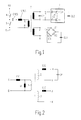
- Fig. 1 shows a more detailed explanation of the problem of "cross regulation" Voltage converter for converting an input voltage UB into a high one DC voltage and another supply voltage.
- This voltage converter contains two switches 4, 5 arranged in series, which act as chopper switches between the input voltage UB and ground 6 alternately periodically conductive and locked.
- Parallel to the second of these switches with the Reference numeral 5 is the series connection of a resonance capacitance CRES, one Resonance inductance LRES and the primary winding of a transformer T connected, which is located between nodes A and B.
- the Resonance capacitance CRES and the resonance inductance LRES are elements of one Input resonance circuit of the voltage converter, in which also the primary winding of the transformer T is included.
- the transformer T has two secondary windings, a first of which Nodes H and V and a second at nodes J and K is led. Of the Transformer T is at nodes H and V to deliver one AC of high amplitude and at nodes J and K for delivery dimensioned another AC voltage.
- the first secondary winding between nodes H and V is therefore also called a high voltage winding designated.
- the further AC voltage on the second secondary winding between the nodes J and K has a much lower amplitude; in the Contrary to the AC voltage of high amplitude (high voltage) on the first Secondary winding is also referred to below as low voltage.
- the first output circuit which is the first secondary winding between the Including nodes H and V is to provide the high DC voltage designed
- the second output circuit which is the second secondary winding between including nodes J and K is to supply the others Supply voltage designed.
- the first output circuit comprises that in FIG. 1 illustrated voltage converter a voltage multiplier 7, the output is connected to a load capacity CL2, at which the high DC voltage sets. There is a between the nodes H and V.
- Parallel capacitance CP inserted depending on the design of the voltage converter by the parasitic winding capacitance of the first secondary winding Transformer T in the first output circuit or by a separate component be educated.
- the output circuit of the second secondary winding 1 comprises a bridge rectifier, the four Contains diodes D1, D2, D3 and D4. This bridge rectifier is on the output side connected to a load capacity CL3, on which the other is in operation Sets supply voltage.
- FIG. 2 shows an equivalent circuit diagram for the transformer T.
- This includes between nodes A and B as an equivalent circuit for the primary winding a series connection of a primary leakage inductance LS1 with a Parallel connection of a main inductance LH of the transformer T and one Primary winding 1 of an ideal transformer.
- This includes on the secondary side 2 for the first secondary winding, the winding 2 of the ideal transformer in series with a secondary leakage inductance LS2 between the nodes H and V and accordingly a series connection of one another secondary winding 3 of the ideal transformer with its associated secondary-side leakage inductance LS3 between the nodes J and K.
- Aus The values can be found in the technical data of the transformer T to be used determine clearly for the leakage inductances.
- the equivalent circuit diagram of the Fig. 2 is also the parallel capacitance CP to the first secondary winding 2 between the nodes H and V are drawn.
- FIG. 3 Another explanation is given in FIG. 3 to explain the problem of "cross regulation" Simplification of the equivalent circuit diagram of the transformer T together with the most important other elements of the voltage converter shown in Fig. 1.
- the Simplification of the equivalent circuit diagram is that the secondary side Elements of the transformer T with the associated gear ratios the primary side of the transformer T are converted so that a simplified, galvanically coupled equivalent circuit diagram results.
- LS22 is the secondary leakage inductance LS2, transformed on the primary side, designated.
- LS33 denotes the leakage inductance LS3 on the secondary side, transformed to the primary side of the transformer T.
- CP22 the Parallel capacitance CP in its on the primary side of the transformer T transformed form.
- H22, V22, J33 and K33 designate accordingly the nodes corresponding to the nodes H, V, J and K respectively transformed circuit. 1 during operation of the voltage converter 3 between the nodes A and B for the equivalent circuit of FIG Voltage uAB, the voltage uH22V22 between nodes H22 and V22 and the voltage uJ33K33 between the nodes J33 and K33.
- the Primary circuit of the voltage converter i.e. the input resonance circuit with the The primary winding of the transformer T has been further simplified in FIG. 3. So is the leakage inductance LS1 with the resonance inductance LRES to one resulting resonance inductance LS1RES have been summarized. Since the LH's main inductance can usually be regarded as high impedance, it is in Fig. 3 not shown. A current i flows in the input resonance circuit during operation.
- Fig. 4 shows the operation of the voltage converter according to Fig. 1 in 3 and the current i im Input resonant circuit.
- the display begins at a time ts at which the transformed parallel capacitance CP22 is completely discharged.
- The is accordingly Voltage uH22V22 at time ts is zero.
- the voltage is correct in a first approximation uAB corresponds to the voltage uH22V22 in this operating state. Both rise starting at time ts starting from zero.
- the described operating state changes at time t0, at which the Parallel capacitance CP22 is charged so far that the voltage uAB and thus the Voltage uJ33K33 reach a value U which is the further supply DC voltage to which the load capacity CL3 is charged during operation, transforms to the primary side of the transformer T.
- the bridge rectifier D1, D2, D3, D4 conductive, and the voltage uJ33K33 remains at the value U.
- the equivalent circuit diagram for this operating case is shown in FIG. 5, in the rest of the elements already explained with matching reference numerals are provided.
- FIG. 6 A section of FIG. 6 explains the rise in voltage uH22V22 shown from the equivalent circuit of Fig. 3, wherein those already described Elements are again provided with matching reference numerals.
- the one in Fig. 6 Excerpt shown includes the transformed secondary leakage inductance LS22 and the transformed parallel capacitance CP22. It turns out that this E elements in the described operating situation a series connection from one Form inductance and a capacitance to which at time t0 Voltage jump corresponding to the voltage U is applied.
- the tension that forms on the parallel capacitance CP22 transformed on the primary side has a sinusoidal curve, the amplitude of which is proportional to the value of the Current i in the input resonance circuit at time t0 and inversely proportional to the value of the transformed parallel capacitance is CP22. Besides, this is Amplitude inversely proportional to the period of the sinusoidal Voltage curve, which in turn is derived from the reciprocal of the square root of the Product of the transformed parallel capacitance CP22 and the transformed Scattering inductance LS22 determined.
- the voltage surge i.e. the amplitude of the sinusoidal curve of the voltage uH22V22 after the time t0, as in Fig.
- the invention now has the task of a voltage converter of the beginning type described with several outputs in such a way that a improved synchronization of the output voltages, i.e. a decreased "Cross regulation", as can be achieved in a conventional manner.
- this object is achieved in a voltage converter Generic type solved by (each) an additional capacity parallel to Secondary winding of the transformer in the (s) Rectifier arrangement (s) having the remaining output circuit (s), the additional capacity (s) is (are) such that you can focus on the Primary side of the transformer transformed value (or transformed values in Sum) essentially with the value of a transformed on the primary side Parallel capacitance of the secondary winding of the transformer from the first Output circuit matches.
- the output circuits can either to different taps of a secondary winding or to individual ones Output circuits or groups of output circuits are electrically isolated Secondary windings are connected.
- the voltage converter can pass through the parallel capacitance from the first output circuit a parasitic winding capacitance, through a separate capacitive component or be a combination of both.
- the current i in the input resonance circuit of the parallel capacity exclusively in the first output circuit to at least one distributed further output circle.
- This causes the current to leakage inductance LS2 or LS22 reduced in the first output circuit at time t0.
- This Decrease also outweighs an increase in current i due to the increase the capacitive load on the secondary side of the transformer T.
- the voltage converter can be reduced the "cross-regulation" of about 30%. This is with very little additional circuitry possible.
- This inventive design of the voltage converter makes it possible to Current through the secondary leakage inductance of the first secondary winding (High voltage winding) of the transformer at the beginning of the voltage surge - see. 4 - to force zero at time t0 in FIG. Because the voltage surge is proportional to this current, it can also be made zero. In order to the "cross regulation" can at least be largely eliminated. To do this reach is at least one of the other output circles of the Voltage converter each assigned an auxiliary circuit, which with its additional Secondary winding of the transformer and its additional capacitor vibrating circuit structure forms.
- the additional rectifier arrangement causes only in the auxiliary circuit a current flows in the time surrounding the beginning of the voltage surge.
- the series connection included in the auxiliary circuit is additional Secondary winding, additional capacitor and additional Rectifier arrangement further parallel to a branch of the rectifier arrangement the relevant output circuit and the load connected to it.
- a tuning resistor can be arranged with which the amplitude of the Current in the auxiliary circuit can be adjusted to a value by which one complete cross-regulation is achieved.
- the circuitry can thus be increased somewhat at least largely rule out cross-regulation.
- this voltage converter is the additional rectifier arrangement or are the additional ones Rectifier arrangements designed as bridge rectifiers.
- Such a Bridge rectifier is preferably equivalent to the rectifier arrangement of the associated output circuit connected to its load.
- the rectifier arrangement (s) of the output circuit are also designed as bridge rectifiers.
- a part of Elements of the bridge rectifier of an output circuit is also part of the additional rectifier arrangement of the same output circuit.
- Voltage converters of the inventive type are advantageous in electrical devices of all kinds can be used in which several loads are fed from one energy source with one of the loads having a higher load than the other loads electrical voltage is to be supplied.
- the invention Voltage converter suitable for use in mains-powered devices such as Monitors, television receivers or the like.
- Fig. 7 shows a circuit arrangement for a voltage converter, the largely corresponds to the circuit arrangement according to FIG. 1. In this respect, the Description of Fig. 1 referenced.
- Fig. 7 shows an additional capacitance CL, which with the second secondary winding of the transformer T connected output circuit between the nodes J and K is arranged parallel to the secondary winding.
- This additional capacity CL is dimensioned so that you with the gear ratio between the second Secondary winding (low voltage winding) and the primary winding of the Transformer T on the primary side converted capacitance value just as large is like the one with the gear ratio between the first secondary winding (High voltage winding) and the primary winding of the transformer T converted capacity value of the parallel capacity CP in the first output circuit between the nodes H and V.
- the current i in the input resonance circuit then distributed at least almost evenly between the two output circles. The excess voltage is thus reduced by about 30%.
- FIG. 8 shows a second exemplary embodiment of an inventive one Voltage converter shown, which is also related to the voltage converter 1 based on.
- This auxiliary circuit includes an additional secondary winding, the also applied to the core of the transformer T and on one side with the Junction J is connected.
- the second connection of this additional Secondary winding forms another node M.
- the further node M is via an additional capacitor CK and, if appropriate, one in Row-arranged tuning resistor RK connected to a node E, which forms a connection point of an additional rectifier arrangement.
- This additional rectifier arrangement includes the diodes D2 and D3 Rectifier arrangement of the output circuit and two further diodes D5 and D6 and is - like the rectifier arrangement of the output circuit - as Bridge rectifier designed.
- the nodes E and K form AC input terminals of the additional rectifier assembly.
- the Nodes J and K form AC input terminals of the Rectifier arrangement D1, D2, D3, D4 of the output circuit, and the load capacity CL3 of this output circuit, on which the further DC supply voltage U can be tapped is connected to nodes P and S, which the DC output terminals of both the additional Rectifier arrangement D2, D3, D5, D6 as well as the rectifier arrangement D1, Form D2, D3, D4 of the output circuit.
- the diode D1 is between the Nodes J and P, D2 between P and K, D3 between K and S, D4 between S and J, D5 between S and E and D6 between E and P.
- D2 and D3 are elements of both the rectifier arrangement of the output circuit and also the additional rectifier arrangement.
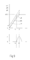
- Fig. 9 To illustrate the operation of the embodiment of FIG. 8 is on Fig. 9 referenced.
- DC voltage uK which is approximately equal to the peak value of the voltage across the additional secondary winding between the nodes M and J and a Has polarity
- the current value of the voltage uMK between the Junctions M and K enlarged.
- the polarity of the voltage uK at the additional Capacitor CK is due to the current caused by this additional Capacitor CK in the previous half period of current i im Input resonance circuit or the voltage uAB has flowed.
- the voltage uMK In the upper part of the 9 is the profile of the voltage uMK for the beginning of a half-wave plotted in which the potential at node M compared to the potential at Node K rises continuously.
- uJK the tension between the Designated nodes J and K, i.e. the on the secondary winding of the Output circuit forming voltage.
- the voltage uMK the ratio of the number of turns between the nodes M and K on the one hand and the nodes J and K on the other hand proportional enlarged.
- the voltage uEK between the nodes E and K, resulting from the sum of the voltages uK and uMK is compared to that The voltage uMK is shifted by the DC voltage uK.
- the voltage uEK increases with the voltage uMK until it is ta at a time the value of the further supply DC voltage UCL3 at the load capacitance CL3 reached.
- the voltage UCL3 is transformed to the primary side of the Transformer T with the associated gear ratio to that already described voltage U.
- Neglecting the diode flux voltages of the Diodes D3 and D6 set a current iK through the additional one at time ta Capacitor CK and thus through the auxiliary circuit, which forms an oscillation, whose period duration by the leakage inductance LSM the additional Secondary winding and the additional capacitor CK is determined.
- the amplitude of this vibration is determined by the value that the Voltage uEK would reach if one followed its course before the time ta extra polished at time t0.
- the time t0 is identical to that in Fig. 4 shown the beginning of the excessive voltage.
- the current iK through the additional capacitor CK is shown in the lower part of FIG. 9 and forms a waveform with a semisine-like course, the maximum of which is a quarter of the period of the mentioned vibration, calculated from Time ta on occurs.
- the semisine-like wave of the described Vibration extends over a time interval that the time t0, i.e. the Includes beginning of voltage surge.
- the time t0 caused by the current i in the input resonance circuit, except for the current in the first secondary winding (high voltage winding) of the transformer T, which in Fig. 8 is entered as iLS2, also the current iK in the additional Secondary winding and the additional capacitor CK.
- time t0 thus competition between the current paths for the currents iLS2 and iK.
- Fig. 10 shows a further embodiment of the invention, which by a Modification of the circuit arrangement according to FIG. 8 has arisen.
- the diode D4 has been omitted, the diode D1 forms without the Auxiliary circuit a one-way rectifier for the from the nodes J and K supplied AC voltage to form the DC voltage UCL3 over the Load capacity CL3.
- the auxiliary group for this arrangement with the additional Secondary winding between nodes M and J, the additional one Capacitor CK and the additional bridge rectifier from diodes D2, D3, D5 and D6 and possibly with the tuning resistor RK is with the auxiliary circuit shown in Fig. 8 identical.
- the exemplary embodiments according to FIGS. 8 and 10 can be expanded by further Secondary windings and the output circuit connected to them are expanded, these output circuits can optionally be equipped with additional auxiliary circuits can.
- the invention provides a significant improvement in synchronism of the output voltages of the output circuits of the voltage converter.
- voltage converters become a broad field of application for Devices opened up where high demands are placed on synchronism be used, for example, for monitors and television receivers.
Abstract
Description
Die Erfindung bezieht sich auf einen Spannungskonverter zum Konvertieren einer Eingangsspannung in wenigstens zwei Ausgangsspannungen, umfassend
- einen Eingangsresonanzkreis, in den eine Primärwicklung eines Transformators einbezogen ist und dem die Eingangsspannung in periodisch wiederkehrenden Zeitintervallen zuführbar ist,
- wenigstens zwei Ausgangskreise, in die je eine Sekundärwicklung oder ein Teil
einer Sekundärwicklung des Transformators einbezogen ist und denen je eine
der Ausgangsspannungen entnehmbar ist, wobei
- eine von einem ersten der Ausgangskreise gelieferte erste der Ausgangsspannungen eine Hochspannung und die übrige(n) Ausgangsspannung(en) (eine) demgegenüber niedrige Spannung(en) bildet (bzw. bilden),
- wenigstens (einer) der die übrige(n) Ausgangsspannung(en) liefernde(n) übrige(n) Ausgangskreis(e) eine Gleichrichteranordnung zum Liefern einer Gleichspannung als Ausgangsspannung aufweist.
- an input resonance circuit, in which a primary winding of a transformer is incorporated and to which the input voltage can be fed in periodically recurring time intervals,
- at least two output circuits, in each of which a secondary winding or part of a secondary winding of the transformer is included and from which one of the output voltages can be inferred, wherein
- a first of the output voltages supplied by a first of the output circuits forms a high voltage and the rest of the output voltage (s) forms a (low) voltage (s),
- at least (one) of the remaining output circuit (s) supplying the remaining output voltage (s) has a rectifier arrangement for supplying a direct voltage as the output voltage.
Aus der deutschen Offenlegungsschrift DE 195 29 941 A1 ist ein Spannungskonverter zur Konvertierung einer Eingangswechselspannung in eine hohe Gleichspannung sowie weitere Versorgungs-Gleichspannungen bekannt. Darin wird die dem Konverter eingangsseitig zugeführte Wechselspannung einer Gleichrichteranordnung zugeführt, deren Ausgangssignal auf zwei hintereinander geschaltete elektronische Schalter geführt ist. Parallel zu einem der elektronischen Schalter ist eine Reihenschaltung aus einer Kapazität, einer Induktivität und einer Primärwicklung eines Transformators geschaltet. Einer Sekundärwicklung des Transformators ist eine ausgangsseitige Kapazität nachgeschaltet. Es ist eine Steuerschaltung vorgesehen, die die Schaltfrequenz der elektronischen Schalter so steuert, daß über der ausgangsseitigen Kapazität eine Gleichspannung gewünschter Höhe abfällt. An dem Transformator sind zusätzliche sekundärseitige Anzapfungen vorgesehen, denen die weiteren Versorgungs-Gleichspannungen über Schaltungsanordnungen zur Spannungsstabilisierung entnehmbar sind.From the German patent application DE 195 29 941 A1 is a Voltage converter for converting an input AC voltage to a high one DC voltage and other DC supply voltages are known. In it the AC voltage supplied to the converter on the input side Rectifier assembly fed, the output signal to two in a row switched electronic switch is guided. Parallel to one of the electronic ones Switch is a series connection of a capacitance, an inductance and one Primary winding of a transformer switched. A secondary winding of the An output-side capacitance is connected downstream of the transformer. It is one Control circuit provided that the switching frequency of the electronic switch controls that a DC voltage is desired above the output-side capacitance Height drops. There are additional taps on the secondary side of the transformer provided, to which the other DC supply voltages Circuit arrangements for voltage stabilization can be removed.
Ist bei einem derartigen Spannungskonverter der erstgenannte Ausgang ein Hochspannungsausgang, der eine gegenüber der eingangsseitig zugeführten Wechselspannung bzw. gegenüber der daraus durch die Gleichrichteranordnung gewonnenen, auf die elektronischen Schalter geführten Gleichspannung bedeutend höhere Ausgangsgleichspannung liefert, und sind ferner die weiteren Versorgungs-Gleichspannungen demgegenüber als Niederspannungsausgänge ausgebildet, wird wegen des dann gewählten höheren Übersetzungsverhältnisses zwischen der Primärwicklung und der Sekundärwicklung des Transformators die ausgangsseitige Kapazität, die eine Parallelkapazität des sogenannten Hochspannungsausgangs des Spannungskonverters bildet, das Betriebsverhalten dieses Spannungskonverters entscheidend bestimmen, da sie zur Primärseite des Transformators mit eben diesem hohen Übersetzungsverhältnis auf einen im Verhältnis hohen Wert transformiert wird. Dagegen haben vergleichbar dimensionierte Parallelkapazitäten an den zusätzlichen sekundärseitigen Anzapfungen, die Niederspannungsausgänge des Spannungskonverters für die vergleichsweise niedrigen weiteren Versorgungs-Gleichspannungen bilden, nur einen geringen Einfluß zur Primärseite des Transformators, da sie entsprechend nur mit den niedrigeren Übersetzungsverhältnissen zur Primärseite transformiert werden.In the case of such a voltage converter, the first-mentioned output is on High voltage output, the one opposite to the input side AC voltage or compared to that resulting from the rectifier arrangement obtained direct voltage on the electronic switch significant provides higher DC output voltage, and are also the other DC supply voltages in contrast, is designed as a low-voltage output because of the higher gear ratio then chosen between the Primary winding and the secondary winding of the transformer on the output side Capacitance, which is a parallel capacitance of the so-called high voltage output of the Voltage converter forms the operating behavior of this voltage converter determine decisively, since they are on the primary side of the transformer with this high gear ratio transformed to a relatively high value becomes. In contrast, similarly dimensioned parallel capacities at the additional taps on the secondary side, the low voltage outputs of the Voltage converter for the comparatively low additional DC supply voltages form, only a slight influence on the primary side of the Transformers, since they only work with the lower ones Gear ratios to the primary side are transformed.
Es zeigt sich, daß bei üblicher Auslegung eines derartigen Spannungskonverters die Parallelkapazität des Hochspannungsausgangs selbst dann noch einen deutlichen, überwiegenden Einfluß auf der Primärseite des Transformators ausübt, wenn sie nicht durch ein zusätzliches Bauelement, sondern nur noch durch die parasitäre Wicklungskapazität der Sekundärwicklung gebildet ist. It turns out that with the usual design of such a voltage converter Parallel capacitance of the high voltage output even then a clear, predominant influence on the primary side of the transformer when it exerts not by an additional component, but only by the parasitic Winding capacity of the secondary winding is formed.
Demgegenüber ist die Wirkung parasitärer Wicklungskapazitäten aus den Sekundärwicklungen bzw. den Teilen der Sekundärwicklung, die mit den Anzapfungen für die weiteren Versorgungs-Gleichspannungen verbunden sind, transformiert auf die Primärseite des Transformators vernachlässigbar gering.In contrast, the effect of parasitic winding capacities from the Secondary windings or the parts of the secondary winding that are connected to the Taps for the further supply DC voltages are connected, transforms to the primary side of the transformer negligible.
Bei einem Spannungskonverter der vorstehend beschriebenen Art tritt bei Belastung der verschiedenen Sekundärwicklungen bzw. Anzapfungen, d.h. bei Entnahme elektrischer Leistung über die Hochspannung bzw. die weiteren Versorgungs-Gleichspannungen, eine gegenseitige Beeinflussung auf, die als "Crossregulation" bezeichnet wird und die sich dadurch bemerkbar macht, daß die Ausgangsspannungen, d.h. die Hochspannung und die weiteren Versorgungs-Gleichspannungen, nicht allein abhängig sind von ihrem gegenseitigen Verhältnis der Windungszahlen der Sekundärwicklungen bzw. der Teile der Sekundärwicklung, sondern auch von ihrer jeweiligen Belastung. Das bedeutet, daß trotz Regelung einer der Gleichspannungen auf einen festen Wert bei den anderen Gleichspannungen Schwankungen auftreten, die von den Belastungen der Ausgänge abhängig sind.In a voltage converter of the type described above occurs under load of the different secondary windings or taps, i.e. on removal electrical power via the high voltage or the further supply DC voltages, a mutual influence that is called "cross-regulation" is called and which is noticeable in that the Output voltages, i.e. the high voltage and the other DC supply voltages, are not solely dependent on their mutual relationship Number of turns of the secondary windings or parts of the secondary winding, but also of their respective loads. That means that despite regulation a of the DC voltages to a fixed value for the other DC voltages Fluctuations occur that depend on the loads on the outputs.
Zwar kann versucht werden, diese Schwankungen zu begrenzen, indem die Streuinduktivitäten der Sekundärwicklungen bzw. der Teile der Sekundärwicklung des Transformators so weit wie möglich verringert werden. Dem sind jedoch Grenzen gesetzt, insbesondere durch die Formgebung des Kerns und des Spulenkörpers des Transformators, durch die Anforderung an eine Spannungsisolierung der einzelnen Wicklungen des Transformators gegeneinander und durch die Mindestanzahl der Windungen der einzelnen Wicklungen, die unter anderem durch die höchst zulässige magnetische Induktion im Kern bestimmt wird. In der Praxis führt dies dazu, daß für bestimmte Anwendungen der beschriebenen Spannungskonverter und die dafür benötigte Auslegung des Transformators die zugleich gestellten Anforderungen an einen Gleichlauf der sekundärseitig abgegebenen Spannungen nicht erfüllt werden können. Das bedeutet, daß die sogenannte Crossregulation bei solchen Spannungskonvertern nicht im vorgeschriebenen Rahmen gehalten werden kann und dadurch der Spannungskonverter der beschriebenen Art für die genannte Anwendung nicht brauchbar ist.One can try to limit these fluctuations by the Stray inductances of the secondary windings or parts of the secondary winding of the transformer can be reduced as much as possible. However, that is Set limits, particularly through the shape of the core and the Coil body of the transformer, by the requirement of a Voltage isolation of the individual windings of the transformer against each other and by the minimum number of turns of the individual windings, which under is determined by the maximum permissible magnetic induction in the core. In practice, this leads to the described for certain applications Voltage converter and the required design of the transformer At the same time, there are requirements for synchronism on the secondary side given voltages can not be met. That means that so-called cross-regulation in such voltage converters not in prescribed framework can be kept and thereby the Voltage converter of the type described for the application mentioned not is useful.
Fig. 1 zeigt zur näheren Erläuterung des Problems der "Crossregulation" einen
Spannungskonverter zum Konvertieren einer Eingangsspannung UB in eine hohe
Gleichspannung und eine weitere Versorgungsspannung. Dieser Spannungskonverter
enthält zwei in Reihe angeordnete Schalter 4, 5, die als Zerhackerschalter zwischen
der Eingangsspannung UB und Masse 6 wechselweise periodisch leitend und
gesperrt geschaltet werden. Parallel zum zweiten dieser Schalter mit dem
Bezugszeichen 5 ist die Reihenschaltung aus einer Resonanzkapazität CRES, einer
Resonanzinduktivität LRES und der Primärwicklung eines Transformators T
angeschlossen, die sich zwischen Knotenpunkten A und B befindet. Die
Resonanzkapazität CRES und die Resonanzinduktivität LRES sind Elemente eines
Eingangsresonanzkreises des Spannungskonverters, in den auch die Primärwicklung
des Transformators T einbezogen ist.Fig. 1 shows a more detailed explanation of the problem of "cross regulation"
Voltage converter for converting an input voltage UB into a high one
DC voltage and another supply voltage. This voltage converter
contains two
Der Transformator T weist zwei Sekundärwicklungen auf, von denen eine erste an Knotenpunkte H und V und eine zweite an Knotenpunkte J und K geführt ist. Der Transformator T ist an den Knotenpunkten H und V zum Liefern einer Wechselspannung hoher Amplitude und an den Knotenpunkten J und K zum Liefern einer weiteren Wechselspannung dimensioniert. Die erste Sekundärwicklung zwischen den Knotenpunkten H und V wird daher auch als Hochspannungswicklung bezeichnet. Die weitere Wechselspannung an der zweiten Sekundärwicklung zwischen den Knotenpunkten J und K hat eine wesentlich niedrigere Amplitude; im Gegensatz zu der Wechselspannung hoher Amplitude (Hochspannung) an der ersten Sekundärwicklung wird sie im folgenden auch als Niederspannung bezeichnet.The transformer T has two secondary windings, a first of which Nodes H and V and a second at nodes J and K is led. Of the Transformer T is at nodes H and V to deliver one AC of high amplitude and at nodes J and K for delivery dimensioned another AC voltage. The first secondary winding between nodes H and V is therefore also called a high voltage winding designated. The further AC voltage on the second secondary winding between the nodes J and K has a much lower amplitude; in the Contrary to the AC voltage of high amplitude (high voltage) on the first Secondary winding is also referred to below as low voltage.
Jede der Sekundärwicklungen des Transformators T ist in einen Ausgangskreis
einbezogen. Der erste Ausgangskreis, der die erste Sekundärwicklung zwischen den
Knotenpunkten H und V einbezieht, ist zum Liefern der hohen Gleichspannung
ausgelegt, und der zweite Ausgangskreis, der die zweite Sekundärwicklung zwischen
den Knotenpunkten J und K einbezieht, ist zum Liefern der weiteren
Versorgungsspannung ausgelegt. Der erste Ausgangskreis umfaßt in dem in Fig. 1
dargestellten Spannungskonverter einen Spannungsvervielfacher 7, dessen Ausgang
mit einer Lastkapazität CL2 verbunden ist, an der sich im Betrieb die hohe
Gleichspannung einstellt. Zwischen den Knotenpunkten H und V ist eine
Parallelkapazität CP eingefügt, die je nach Auslegung des Spannungskonverters
durch die parasitäre Wicklungskapazität der ersten Sekundärwicklung des
Transformators T im erste Ausgangskreis oder durch ein gesondertes Bauelement
gebildet sein.Each of the secondary windings of the transformer T is in an output circuit
involved. The first output circuit, which is the first secondary winding between the
Including nodes H and V is to provide the high DC voltage
designed, and the second output circuit, which is the second secondary winding between
including nodes J and K is to supply the others
Supply voltage designed. The first output circuit comprises that in FIG. 1
illustrated voltage converter a
Der die zweite Sekundärwicklung einbeziehende Ausgangskreis des
Spannungskonverters nach Fig. 1 umfaßt einen Brückengleichrichter, der vier
Dioden D1, D2, D3 und D4 enthält. Dieser Brückengleichrichter ist ausgangsseitig
mit einer Lastkapazität CL3 verbunden, an der sich im Betrieb die weitere
Versorgungsspannung einstellt.The output circuit of the second
In der Darstellung nach Fig. 1 ist zwischen den Knotenpunkten J und K keine Kapazität eingetragen. Durch die Wahl des Übersetzungsverhältnisses zwischen der zweiten Sekundärwicklung zwischen den Knotenpunkten J und K und der Primärwicklung zwischen den Knotenpunkten A und B einerseits sowie des Übersetzungsverhältnisses zwischen der ersten Sekundärwicklung zwischen den Knotenpunkten H und V und der Primärwicklung andererseits ergibt sich bei diesem dargestellten Spannungskonverter, daß der Einfluß einer parasitären Wicklungskapazität der zweiten Sekundärwicklung, transformiert zur Primärseite des Transformators T, gegenüber der Parallelkapazität CP vernachlässigbar ist.In the illustration according to FIG. 1 there is none between the nodes J and K. Capacity entered. By choosing the gear ratio between the second secondary winding between the nodes J and K and the Primary winding between nodes A and B on the one hand and the Gear ratio between the first secondary winding between the Nodes H and V and the primary winding on the other hand result in this illustrated voltage converter that the influence of a parasitic Winding capacity of the second secondary winding, transformed to the primary side of the Transformer T, is negligible compared to the parallel capacitance CP.
Zur Erläuterung der Wirkungsweise des Spannungskonverters nach Fig. 1 ist in
Fig. 2 ein Ersatzschaltbild für den Transformator T dargestellt. Dieses umfaßt
zwischen den Knotenpunkten A und B als Ersatzschaltbild für die Primärwicklung
eine Reihenschaltng aus einer primären Streuinduktivität LS1 mit einer
Parallelschaltung einer Hauptinduktivität LH des Transformators T und einer
Primärwicklung 1 eines idealen Transformators. Sekundärseitig umfaßt das
Ersatzschaltbild gemäß Fig. 2 für die erste Sekundärwicklung die Wicklung 2 des
idealen Transformators in Reihe mit einer sekundärseitigen Streuinduktivität LS2
zwischen den Knotenpunkten H und V und entsprechend eine Reihenschaltung einer
weiteren Sekundärwicklung 3 des idealen Transformators mit ihrer zugehörigen
sekundärseitigen Streuinduktivität LS3 zwischen den Knotenpunkten J und K. Aus
den technischen Daten des zu verwendenden Transformators T lassen sich die Werte
für die Streuinduktivitäten jeweils eindeutig bestimmen. In das Ersatzschaltbild der
Fig. 2 ist ferner die Parallelkapazität CP zur ersten Sekundärwicklung 2 zwischen
den Knotenpunkten H und V eingezeichnet.1 to explain the mode of operation of the voltage converter according to FIG
Fig. 2 shows an equivalent circuit diagram for the transformer T. This includes
between nodes A and B as an equivalent circuit for the primary winding
a series connection of a primary leakage inductance LS1 with a
Parallel connection of a main inductance LH of the transformer T and one
Zur Erläuterung des Problems der "Crossregulation" ist in Fig. 3 eine weitere Vereinfachung des Ersatzschaltbildes des Transformators T zusammen mit den wichtigsten sonstigen Elementen des Spannungskonverters aus Fig. 1 dargestellt. Die Vereinfachung des Ersatzschaltbildes besteht darin, daß die sekundärseitigen Elementen des Transformators T mit den zugehörigen Übersetzungsverhältnissen auf die Primärseite des Transformators T umgerechnet sind, so daß sich ein vereinfachtes, galvanisch gekoppeltes Ersatzschaltbild ergibt. Darin sind bereits beschriebene Elemente mit übereinstimmenden Bezugszeichen versehen. Mit LS22 ist die sekundärseitige Streuinduktivität LS2, transformiert auf die Primärseite, bezeichnet. Entsprechend bezeichnet LS33 die sekundärseitige Streuinduktivität LS3, transformiert auf die Primärseite des Transformators T. Mit CP22 ist die Parallelkapazität CP in ihrer auf die Primärseite des Transformators T transformierten Form benannt. Entsprechend bezeichnen H22, V22, J33 und K33 die den Knotenpunkten H, V, J bzw. K entsprechenden Knotenpunkte der transformierten Schaltung. Im Betrieb des Spannungskonverters nach Fig. 1 ergeben sich für das Ersatzschaltbild der Fig. 3 zwischen den Knotenpunkten A und B die Spannung uAB, zwischen den Knotenpunkten H22 und V22 die Spannung uH22V22 und zwischen den Knotenpunkten J33 und K33 die Spannung uJ33K33. Der Primärkreis des Spannungskonverters, d.h. der Eingangsresonanzkreis mit der Primärwicklung des Transformators T, ist in Fig. 3 weiter vereinfacht worden. So ist die Streuinduktivität LS1 mit der Resonanzinduktivität LRES zu einer resultierenden Resonanzinduktivität LS1RES zusammengefaßt worden. Da die Hauptinduktivität LH in der Regel als hochohmig betrachtet werden kann, ist sie in Fig. 3 nicht dargestellt. Im Eingangsresonanzkreis fließt im Betrieb ein Strom i.Another explanation is given in FIG. 3 to explain the problem of "cross regulation" Simplification of the equivalent circuit diagram of the transformer T together with the most important other elements of the voltage converter shown in Fig. 1. The Simplification of the equivalent circuit diagram is that the secondary side Elements of the transformer T with the associated gear ratios the primary side of the transformer T are converted so that a simplified, galvanically coupled equivalent circuit diagram results. In there are already elements described with matching reference numerals. With LS22 is the secondary leakage inductance LS2, transformed on the primary side, designated. Correspondingly, LS33 denotes the leakage inductance LS3 on the secondary side, transformed to the primary side of the transformer T. With CP22 the Parallel capacitance CP in its on the primary side of the transformer T transformed form. H22, V22, J33 and K33 designate accordingly the nodes corresponding to the nodes H, V, J and K respectively transformed circuit. 1 during operation of the voltage converter 3 between the nodes A and B for the equivalent circuit of FIG Voltage uAB, the voltage uH22V22 between nodes H22 and V22 and the voltage uJ33K33 between the nodes J33 and K33. Of the Primary circuit of the voltage converter, i.e. the input resonance circuit with the The primary winding of the transformer T has been further simplified in FIG. 3. So is the leakage inductance LS1 with the resonance inductance LRES to one resulting resonance inductance LS1RES have been summarized. Since the LH's main inductance can usually be regarded as high impedance, it is in Fig. 3 not shown. A current i flows in the input resonance circuit during operation.
Fig. 4 zeigt für den Betrieb des Spannungskonverters nach Fig. 1 die im Ersatzschaltbild der Fig. 3 eingetragenen Spannungen und den Strom i im Eingangsresonanzkreis. Die Darstellung beginnt zu einem Zeitpunkt ts, an dem die transformierte Parallelkapazität CP22 vollständig entladen ist. Entsprechend ist die Spannung uH22V22 zum Zeitpunkt ts gleich Null. Bei einer verhältnismäßig kleinen transformierten Streuinduktivität LS22 und langsamer Änderung des Stromes i kann die an der transformierten Streuinduktivität LS22 entstehende Spannung in erster Näherung vernachlässigt werden. Somit stimmt in erster Näherung die Spannung uAB in diesem Betriebszustand mit der Spannung uH22V22 überein. Beide steigen, beginnend zum Zeitpunkt ts von Null beginnend an. In diesem Betriebszustand ist der Brückengleichrichter D1, D2, D3, D4 noch gesperrt, im zweiten Ausgangskreis über die Knotenpunkte J33, K33 fließt noch kein Strom und die Spannung uJ33K33 folgt dem zeitlichen Verlauf der Spannung uAB unmittelbar. Der Strom i fließt vollständig in die Parallelkapazität CP22 und lädt diese auf.Fig. 4 shows the operation of the voltage converter according to Fig. 1 in 3 and the current i im Input resonant circuit. The display begins at a time ts at which the transformed parallel capacitance CP22 is completely discharged. The is accordingly Voltage uH22V22 at time ts is zero. With a relatively small one transformed leakage inductance LS22 and slow change in current i can the voltage generated at the transformed leakage inductance LS22 in the first Approximation are neglected. Thus, the voltage is correct in a first approximation uAB corresponds to the voltage uH22V22 in this operating state. Both rise starting at time ts starting from zero. Is in this operating state the bridge rectifier D1, D2, D3, D4 still locked, in the second output circuit No current or voltage uJ33K33 flows through nodes J33, K33 follows the time course of the voltage uAB immediately. The current i flows completely into the parallel capacity CP22 and charges it.
Der geschilderte Betriebszustand ändert sich zum Zeitpunkt t0, an dem die Parallelkapazität CP22 so weit aufgeladen ist, daß die Spannung uAB und damit die Spannung uJ33K33 einen Wert U erreichen, der die weitere Versorgungs-Gleichspannung darstellt, auf die im Betrieb die Lastkapazität CL3 aufgeladen ist, transformiert auf die Primärseite des Transformators T. Zum Zeitpunkt t0 wird somit der Brückengleichrichter D1, D2, D3, D4 leitend, und die Spannung uJ33K33 verharrt auf dem Wert U. Das Ersatzschaltbild für diesen Betriebsfall zeigt Fig. 5, in der im übrigen bereits erläuterte Elemente mit übereinstimmenden Bezugszeichen versehen sind.The described operating state changes at time t0, at which the Parallel capacitance CP22 is charged so far that the voltage uAB and thus the Voltage uJ33K33 reach a value U which is the further supply DC voltage to which the load capacity CL3 is charged during operation, transforms to the primary side of the transformer T. At time t0 thus the bridge rectifier D1, D2, D3, D4 conductive, and the voltage uJ33K33 remains at the value U. The equivalent circuit diagram for this operating case is shown in FIG. 5, in the rest of the elements already explained with matching reference numerals are provided.
Wird im Ersatzschaltbild der Fig. 5 auch die an der transformierten Streuinduktivität LS33 entstehende Spannung vernachlässig, verharrt die Spannung uAB vom Zeitpunkt t0 an auf dem Wert U. Bei einem Spannungskonverter ohne den Effekt der "Crossregulation" würde auch die Spannung uH22V22 vom Zeitpunkt t0 an auf dem Wert U beharren. Es zeigt sich jedoch, daß auch nach dem Zeitpunkt t0 die Spannung an der (transformierten) Parallelkapazität CP22 weiter ansteigt. Dieser Verlauf ist in Fig. 4 dargestellt.5 in the equivalent circuit diagram of the transformed leakage inductance LS33 resulting voltage neglect, the voltage uAB remains Time t0 on at the value U. With a voltage converter without the effect the "cross regulation" would also increase the voltage uH22V22 from time t0 insist on the value U. It turns out, however, that even after the time t0 Voltage on the (transformed) parallel capacitance CP22 continues to rise. This The course is shown in FIG. 4.
Zur Erläuterung des Ansteigens der Spannung uH22V22 ist in Fig. 6 ein Ausschnitt aus dem Ersatzschaltbild der Fig. 3 dargestellt, worin die bereits beschriebenen Elemente wieder mit übereinstimmenden Bezugszeichen versehen sind. Der in Fig. 6 dargestellte Ausschnitt umfaßt die transformierte sekundärseitige Streuinduktivität LS22 und die transformierte Parallelkapazität CP22. Es zeigt sich, daß diese Eelemente in der beschriebenen Betriebssituation eine Reihenschaltung aus einer Induktivität und einer Kapazität bilden, an die zum Zeitpunkt t0 ein Spannungssprung entsprechend der Spannung U angelegt wird. Die Spannung, die sich an der auf die Primärseite transformierten Parallelkapazität CP22 ausbildet, weist einen sinusförmigen Verlauf auf, dessen Amplitude proportional zum Wert des Stromes i im Eingangsresonanzkreis zum Zeitpunkt t0 und umgekehrt proportional zum Wert der transformierten Parallelkapazität CP22 ist. Außerdem ist diese Amplitude umgekehrt proportional zur Periodendauer des sinusförmigen Spannungsverlaufs, die sich wiederum aus dem Kehrwert der Quadratwurzel des Produktes aus der transformierten Parallelkapazität CP22 und der transformierten Streuinduktivität LS22 bestimmt. Die Spannungsüberhöhung, d.h. die Amplitude des sinusförmigen Verlaufes der Spannung uH22V22 nach dem Zeitpunkt t0, wie in Fig. 4 abgebildet, ist somit proportional zum Strom i im Eingangsresonanzkreis und damit gemäß dem Ersatzschaltbild der Fig. 3 in der transformierten, sekundären Streuinduktivität LS22 zum Zeitpunkt t0 sowie proportional zur Quadratwurzel dieser transformierten Streuinduktivität LS22 und umgekehrt proportional zur Quadratwurzel der transformierten Parallelkapazität CP22. Diese Spannungsüberhöhung bewirkt eine störende "Crossregulation".A section of FIG. 6 explains the rise in voltage uH22V22 shown from the equivalent circuit of Fig. 3, wherein those already described Elements are again provided with matching reference numerals. The one in Fig. 6 Excerpt shown includes the transformed secondary leakage inductance LS22 and the transformed parallel capacitance CP22. It turns out that this E elements in the described operating situation a series connection from one Form inductance and a capacitance to which at time t0 Voltage jump corresponding to the voltage U is applied. The tension that forms on the parallel capacitance CP22 transformed on the primary side, has a sinusoidal curve, the amplitude of which is proportional to the value of the Current i in the input resonance circuit at time t0 and inversely proportional to the value of the transformed parallel capacitance is CP22. Besides, this is Amplitude inversely proportional to the period of the sinusoidal Voltage curve, which in turn is derived from the reciprocal of the square root of the Product of the transformed parallel capacitance CP22 and the transformed Scattering inductance LS22 determined. The voltage surge, i.e. the amplitude of the sinusoidal curve of the voltage uH22V22 after the time t0, as in Fig. 4 is thus proportional to the current i in the input resonance circuit and thus according to the equivalent circuit diagram of FIG. 3 in the transformed, secondary Stray inductance LS22 at time t0 and proportional to the square root this transformed leakage inductance LS22 and inversely proportional to Square root of the transformed parallel capacitance CP22. This Excess voltage causes a disturbing "cross regulation".
Da der Strom durch die transformierte Streuinduktivität LS22 zum Zeitpunkt t0 dem Strom i im Eingangsresonanzkreis entspricht, wird er bestimmt durch die aufgenommene Leistung des Spannungskonverters und durch dessen Dimensionierung. Die Abhängigkeit der Spannungsüberhöhung von den Elementen des Spannungskonverters in der beschriebenen Form könnte zu dem Versuch führen, den Wert der Parallelkapazität CP zu vergrößern oder die Streuinduktivität LS2 zu verkleinern. Eine Verringerung der Spannungsüberhöhung wird jedoch dadurch nicht erreicht, da eine Vergrößerung der Parallelkapazität CP unmittelbar eine Vergrößerung des Stromes i zum Zeitpunkt t0 nach sich zieht. Weiterhin sind einer Verringerung der Streuinduktivität LS2 wie eingangs erläutert enge Grenzen gesetzt. Ohne eine Verringerung der Spannungsüberhöhung wird jedoch auch keine Verringerung der "Crossregulation" möglich.Since the current through the transformed leakage inductance LS22 at time t0 Current i corresponds to the input resonance circuit, it is determined by the power consumed by the voltage converter and by its Sizing. The dependence of the voltage increase on the elements of the voltage converter in the form described could lead to the attempt to increase the value of the parallel capacitance CP or to increase the leakage inductance LS2 downsize. However, this does not reduce the voltage overshoot achieved because an increase in the parallel capacity CP immediately one The current i increases at time t0. Furthermore, one Reduction of the leakage inductance LS2, as explained in the introduction, sets narrow limits. Without a reduction in the voltage surge, however, none will Cross-regulation can be reduced.
Die Erfindung hat nun die Aufgabe, einen Spannungskonverter der eingangs beschriebenen Art mit mehreren Ausgängen in der Weise auszubilden, daß ein verbesserter Gleichlauf der Ausgangsspannungen, d.h. eine verringerte "Crossregulation", als in herkömmlicher Weise erreichbar erzielt wird.The invention now has the task of a voltage converter of the beginning type described with several outputs in such a way that a improved synchronization of the output voltages, i.e. a decreased "Cross regulation", as can be achieved in a conventional manner.
Erfindungsgemäß wird diese Aufgabe bei einem Spannungskonverter der gattungsgemäßen Art gelöst durch (je) eine zusätzliche Kapazität parallel zur Sekundärwicklung des Transformators in dem (bzw. den) die Gleichrichteranordnung(en) aufweisenden übrigen Ausgangskreis(en), wobei die zusätzliche(n) Kapazität(en) derart bemessen ist (bzw. sind), daß ihr(e) auf die Primärseite des Transformators transformierter Wert (bzw. transformierten Werte in Summe) im wesentlichen mit dem auf die Primärseite transformierten Wert einer Parallelkapazität der Sekundärwicklung des Transformators aus dem ersten Ausgangskreis übereinstimmt.According to the invention, this object is achieved in a voltage converter Generic type solved by (each) an additional capacity parallel to Secondary winding of the transformer in the (s) Rectifier arrangement (s) having the remaining output circuit (s), the additional capacity (s) is (are) such that you can focus on the Primary side of the transformer transformed value (or transformed values in Sum) essentially with the value of a transformed on the primary side Parallel capacitance of the secondary winding of the transformer from the first Output circuit matches.
Bei dem erfindungsgemäßen Spannungskonverter können die Ausgangskreise entweder an verschiedene Anzapfungen einer Sekundärwicklung oder an für einzelne Ausgangskreise oder Gruppen von Ausgangskreisen galvanisch getrennte Sekundärwicklungen angeschlossen sein. Je nach bevorzugter Dimensionierung des Spannungskonverters kann die Parallelkapazität aus dem ersten Ausgangskreis durch eine parasitäre Wicklungskapazität, durch ein gesondertes kapazitives Bauelement oder durch eine Kombination aus beiden gebildet sein.In the voltage converter according to the invention, the output circuits can either to different taps of a secondary winding or to individual ones Output circuits or groups of output circuits are electrically isolated Secondary windings are connected. Depending on the preferred dimensioning of the Voltage converter can pass through the parallel capacitance from the first output circuit a parasitic winding capacitance, through a separate capacitive component or be a combination of both.
Durch die zusätzliche Kapazität bzw. die zusätzlichen Kapazitäten in wenigstens einem der übrigen Ausgangskreise wird der Strom i im Eingangsresonanzkreis von der Parallelkapazität ausschließlich im ersten Ausgangskreis auf wenigstens einen weiteren Ausgangskreis verteilt. Dadurch wird der Strom in der Streuinduktivität LS2 bzw. LS22 im ersten Ausgangskreis zum Zeitpunkt t0 vermindert. Diese Verminderung überwiegt auch eine Vergrößerung des Stromes i durch die Zunahme der kapazitiven Belastung auf der Sekundärseite des Transformators T. Insgesamt wird somit die Spannungsüberhöhung verringert, ohne die Werte für die Streuinduktivität LS22 oder die Parallelkapazität CP22 zu verändern. Durch die erfindungsgemäße Ausbildung des Spannungskonverters läßt sich eine Verringerung der "Crossregulation" von etwa 30 % erreichen. Dies ist mit einem sehr geringen zusätzlichen Schaltungsaufwand möglich.At least through the additional capacity or the additional capacities one of the remaining output circuits, the current i in the input resonance circuit of the parallel capacity exclusively in the first output circuit to at least one distributed further output circle. This causes the current to leakage inductance LS2 or LS22 reduced in the first output circuit at time t0. This Decrease also outweighs an increase in current i due to the increase the capacitive load on the secondary side of the transformer T. Overall the voltage increase is thus reduced without the values for the Change leakage inductance LS22 or the parallel capacitance CP22. Through the According to the invention, the voltage converter can be reduced the "cross-regulation" of about 30%. This is with very little additional circuitry possible.
Die Aufgabe wird bei einem Spannungskonverter der gattungsgemäßen Art ferner gelöst durch (je) einen Hilfskreis in dem (bzw. den) die Gleichrichteranordnung(en) aufweisenden übrigen Ausgangskreis(en), wobei
- jeder Hilfskreis eine zusätzliche Sekundärwicklung des Transformators umfaßt, die mit einem zusätzlichen Kondensator und einer zusätzlichen Gleichrichteranordnung in einer Reihenschaltung angeordnet ist und
- diese Reihenschaltung parallel zu einem Zweig der Gleichrichteranordnung des betreffenden Ausgangskreises sowie einer mit diesem verbundenen Last angeordnet ist.
- each auxiliary circuit comprises an additional secondary winding of the transformer, which is arranged in a series circuit with an additional capacitor and an additional rectifier arrangement, and
- this series circuit is arranged parallel to a branch of the rectifier arrangement of the output circuit in question and a load connected to it.
Durch diese erfinderische Ausbildung des Spannungskonverters ist es möglich, den Strom durch die sekundärseitige Streuinduktivität der ersten Sekundärwicklung (Hochspannungswicklung) des Transformators zu Beginn der Spannungsüberhöhung - vgl. Zeitpunkt t0 in Fig. 4 - zu Null zu erzwingen. Da die Spannungsüberhöhung proportional zu diesem Strom ist, kann sie ebenfalls zu Null gemacht werden. Damit kann die "Crossregulation" wenigstens weitgehend beseitigt werden. Um dies zu erreichen, ist wenigstens einem der übrigen Ausgangskreise des Spannungskonverters je ein Hilfskreis zugeordnet, der mit seiner zusätzlichen Sekundärwicklung des Transformators und seinem zusätzlichen Kondensator ein schwingfähiges Schaltungsgebilde formt. Dieses ist über eine zusätzliche Gleichrichteranordnung mit der Gleichrichteranordnung des zugeordneten Ausgangskreises und der daran angeschlossenen Last derart verbunden, daß in der zusätzlichen Sekundärwicklung des Transformators zu Beginn der Spannungsüberhöhung ein Strom auftritt, der in Konkurrenz zu dem Strom durch die Streuinduktivität der Sekundärwicklung des Ausgangskreises tritt. Durch eine entsprechende Dimensionierung der zusätzlichen Sekundärwicklung und des zusätzlichen Kondensators des Hilfskreises (bzw. der Hilfskreise, sofern mehrere Ausgangskreise vorhanden sind und von ihnen mehrere mit je einem Hilfskreis ausgestattet sind) kann erreicht werden, daß der Strom in der sekundärseitigen Streuinduktivität der Sekundärwicklung des Ausgangskreises zu Beginn der Spannungsüberhöhung zu Null wird. Dadurch wird die Spannungsüberhöhung und somit auch die durch sie verursachte Crossregulation wenigstens nahezu vollständig unterbunden. Die zusätzliche Gleichrichteranordnung bewirkt, daß im Hilfskreis nur in der zeitlichen Umgebung des Beginns der Spannungsüberhöhung ein Strom fließt. Zu diesem Zweck ist die vom Hilfskreis umfaßte Reihenschaltung aus zusätzlicher Sekundärwicklung, zusätzlichem Kondensator und zusätzlicher Gleichrichteranordnung ferner parallel zu einem Zweig der Gleichrichteranordnung des betreffenden Ausgangskreises und der mit diesem verbundenen Last angeordnet. Durch einen Vergleich der Spannung an dieser Last mit der im Hilfskreis auftretenden Spannung ist sichergestellt, daß der Stromfluß im Hilfskreis zu Beginn der Spannungsüberhöhung auftritt.This inventive design of the voltage converter makes it possible to Current through the secondary leakage inductance of the first secondary winding (High voltage winding) of the transformer at the beginning of the voltage surge - see. 4 - to force zero at time t0 in FIG. Because the voltage surge is proportional to this current, it can also be made zero. In order to the "cross regulation" can at least be largely eliminated. To do this reach is at least one of the other output circles of the Voltage converter each assigned an auxiliary circuit, which with its additional Secondary winding of the transformer and its additional capacitor vibrating circuit structure forms. This is about an additional one Rectifier arrangement with the rectifier arrangement of the associated Output circuit and the load connected to it in such a way that in the additional secondary winding of the transformer at the beginning of A current surge occurs that competes with the current through the voltage Stray inductance of the secondary winding of the output circuit occurs. By a appropriate dimensioning of the additional secondary winding and the additional capacitor of the auxiliary circuit (or the auxiliary circuits, if several Output circles are available and several of them, each with an auxiliary circuit are equipped) can be achieved that the current in the secondary Stray inductance of the secondary winding of the output circuit at the beginning of the Voltage surge becomes zero. This will increase the voltage and thus the cross-regulation caused by it at least almost completely prevented. The additional rectifier arrangement causes only in the auxiliary circuit a current flows in the time surrounding the beginning of the voltage surge. For this purpose, the series connection included in the auxiliary circuit is additional Secondary winding, additional capacitor and additional Rectifier arrangement further parallel to a branch of the rectifier arrangement the relevant output circuit and the load connected to it. By comparing the voltage on this load with that in the auxiliary circuit occurring voltage ensures that the current flow in the auxiliary circuit at the beginning the voltage surge occurs.
Vorzugsweise kann parallel zu oder in Reihe mit dem zusätzlichen Kondensator im Hilfskreis ein Abstimmwiderstand angeordnet sein, mit dem die Amplitude des Stromes im Hilfskreis auf einen Wert abgestimmt werden kann, durch den eine möglichst vollständige Aufhebung der Crossregulation erreicht wird.Preferably, in parallel with or in series with the additional capacitor Auxiliary circuit a tuning resistor can be arranged with which the amplitude of the Current in the auxiliary circuit can be adjusted to a value by which one complete cross-regulation is achieved.
Erfindungsgemäß läßt sich somit durch einen wenig erhöhten Schaltungsaufwand eine "Crossregulation" wenigstens weitgehend ausschließen.According to the invention, the circuitry can thus be increased somewhat at least largely rule out cross-regulation.
In einer vorteilhaften Weiterbildung dieses erfindungsgemäßen Spannungskonverters ist die zusätzliche Gleichrichteranordnung bzw. sind die zusätzlichen Gleichrichteranordnungen als Brückengleichrichter ausgebildet. Ein solcher Brückengleichrichter ist bevorzugt gleichwirkend wie die Gleichrichteranordnung des zugeordneten Ausgangskreises mit dessen Last verbunden.In an advantageous development of this voltage converter according to the invention is the additional rectifier arrangement or are the additional ones Rectifier arrangements designed as bridge rectifiers. Such a Bridge rectifier is preferably equivalent to the rectifier arrangement of the associated output circuit connected to its load.
In einer weiteren Ausgestaltung des erfindungsgemäßen Spannungskonverters ist (bzw. sind) die Gleichrichteranordnung(en) des Ausgangskreises (bzw. der Ausgangskreise) ebenfalls als Brückengleichrichter ausgebildet. Ein Teil der Elemente des Brückengleichrichters eines Ausgangskreises ist zugleich Teil der zusätzlichen Gleichrichteranordnung desselben Ausgangskreises. In a further embodiment of the voltage converter according to the invention (or are) the rectifier arrangement (s) of the output circuit (or the Output circuits) are also designed as bridge rectifiers. A part of Elements of the bridge rectifier of an output circuit is also part of the additional rectifier arrangement of the same output circuit.
Spannungskonverter der erfinderischen Art sind vorteilhaft in elektrischen Geräten aller Art einsetzbar, in denen mehrere Lasten aus einer Energiequelle gespeist werden, wobei eine der Lasten mit einer gegenüber den übrigen Lasten höheren elektrischen Spannung zu versorgen ist. Insbesondere ist der erfindungsgemäße Spannungskonverter geeignet für den Einsatz in netzgespeisten Geräten wie Monitoren, Fernsehempfängern oder dergleichen.Voltage converters of the inventive type are advantageous in electrical devices of all kinds can be used in which several loads are fed from one energy source with one of the loads having a higher load than the other loads electrical voltage is to be supplied. In particular, the invention Voltage converter suitable for use in mains-powered devices such as Monitors, television receivers or the like.
Ausführungsbeispiele der Erfindung sind in den Fig. 7 bis 10 der Zeichnung
dargestellt und werden im nachfolgenden näher erläutert. Bereits beschriebene
Elemente sind weiterhin mit übereinstimmenden Bezugszeichen versehen. Es zeigen:
Fig. 7 zeigt eine Schaltungsanordnung für einen Spannungskonverter, die weitestgehend der Schaltungsanordnung nach Fig. 1 entspricht. Insoweit wird auf die Beschreibung zu Fig. 1 verwiesen.Fig. 7 shows a circuit arrangement for a voltage converter, the largely corresponds to the circuit arrangement according to FIG. 1. In this respect, the Description of Fig. 1 referenced.
Gegenüber der Schaltungsanordnung nach Fig. 1 enthält das Ausführungsbeispiel der Fig. 7 eine zusätzliche Kapazität CL, welche im mit der zweiten Sekundärwicklung des Transformators T verbundenen Ausgangskreis zwischen den Knotenpunkten J und K parallel zur Sekundärwicklung angeordnet ist. Diese zusätzliche Kapazität CL ist derart bemessen, daß ihr mit dem Übersetzungsverhältnis zwischen der zweiten Sekundärwicklung (Niederspannungswicklung) und der Primärwicklung des Transformators T auf dessen Primärseite umgerechneter Kapazitätswert ebenso groß ist wie der mit dem Übersetzungsverhältnis zwischen der ersten Sekundärwicklung (Hochspannungswicklung) und der Primärwicklung des Transformators T umgerechnete Kapazitätswert der Parallelkapazität CP im ersten Ausgangskreis zwischen den Knotenpunkten H und V. Der Strom i im Eingangsresonanzkreis verteilt sich dann wenigstens nahezu gleichmäßig auf die beiden Ausgangskreise. Die Spannungsüberhöhung reduziert sich damit um etwa 30 %.Compared to the circuit arrangement according to FIG. 1, the exemplary embodiment contains Fig. 7 shows an additional capacitance CL, which with the second secondary winding of the transformer T connected output circuit between the nodes J and K is arranged parallel to the secondary winding. This additional capacity CL is dimensioned so that you with the gear ratio between the second Secondary winding (low voltage winding) and the primary winding of the Transformer T on the primary side converted capacitance value just as large is like the one with the gear ratio between the first secondary winding (High voltage winding) and the primary winding of the transformer T converted capacity value of the parallel capacity CP in the first output circuit between the nodes H and V. The current i in the input resonance circuit then distributed at least almost evenly between the two output circles. The excess voltage is thus reduced by about 30%.
In Fig. 8 ist ein zweites Ausführungsbeispiel für einen erfindungsgemäßen
Spannungskonverter dargestellt, welches sich ebenfalls an den Spannungskonverter
gemäß Fig. 1 anlehnt. Gegenüber Fig. 1 weist die Schaltungsanordnung nach Fig. 8
zu dem mit der zweiten Sekundärwicklung verbundenen Ausgangskreis einen
Hilfskreis auf. Dieser Hilfskreis umfaßt eine zusätzliche Sekundärwicklung, die
ebenfalls auf den Kern des Transformators T aufgebracht und einseitig mit dem
Knotenpunkt J verbunden ist. Der zweite Anschluß dieser zusätzlichen
Sekundärwicklung bildet einen weiteren Knotenpunkt M. Der weitere Knotenpunkt
M ist über einen zusätzlichen Kondensator CK und gegebenenfalls einen dazu in
Reihe angeordneten Abstimmwiderstand RK mit einem Knotenpunkt E verbunden,
der einen Anschlußpunkt einer zusätzlichen Gleichrichteranordnung bildet. Diese
zusätzliche Gleichrichteranordnung umfaßt die Dioden D2 und D3 der
Gleichrichteranordnung des Ausgangskreises sowie zwei weitere Dioden D5 und D6
und ist - wie die Gleichrichteranordnung des Ausgangskreises - als
Brückengleichrichter ausgebildet. Dabei bilden die Knotenpunkte E und K
Wechselspannungs-Eingangsanschlüsse der zusätzlichen Gleichrichteranordnung. Die
Knotenpunkte J und K bilden Wechselspannungs-Eingangsanschlüsse der
Gleichrichteranordnung D1, D2, D3, D4 des Ausgangskreises, und die Lastkapazität
CL3 dieses Ausgangskreises, an der die weitere Versorgungs-Gleichspannung U
abgegriffen werden kann, ist mit Knotenpunkten P und S verbunden, die die
Gleichspannungs-Ausgangsanschlüsse sowohl der zusätzlichen
Gleichrichteranordnung D2, D3, D5, D6 als auch der Gleichrichteranordnung D1,
D2, D3, D4 des Ausgangskreises bilden. Dabei ist die Diode D1 zwischen den
Knotenpunkten J und P, D2 zwischen P und K, D3 zwischen K und S, D4 zwischen
S und J, D5 zwischen S und E sowie D6 zwischen E und P angeordnet. D2 und D3
sind somit Elemente sowohl der Gleichrichteranordnung des Ausgangskreises als
auch der zusätzlichen Gleichrichteranordnung.8 shows a second exemplary embodiment of an inventive one
Voltage converter shown, which is also related to the
In Fig. 8 ist mit LSM die Streuinduktivität der zusätzlichen Sekundärwicklung zwischen den Knotenpunkten M und J bezeichnet; mit 3Z ist in der Ersatzschaltbild-Darstellung der Fig. 8 die ideale zusätzliche Sekundärwicklung des Transformators T benannt, die mit der Streuinduktivität LSM zwischen den Knotenpunkten M und J in Reihe geschaltet ist. Entsprechend ist auch für die erste Sekundärwicklung 2 und ihre Streuinduktivität LS2 in Fig. 8 eine Ersatzschaltbild-Darstellung gewählt worden.8 with LSM is the leakage inductance of the additional secondary winding designated between nodes M and J; with 3Z is in the equivalent circuit diagram 8 the ideal additional secondary winding of the Transformer T named with the leakage inductance LSM between the Junctions M and J is connected in series. The same is true for the first Secondary winding 2 and its leakage inductance LS2 in Fig. 8 is an equivalent circuit diagram representation has been chosen.
Zur Darstellung der Funktionsweise des Ausführungsbeispiels nach Fig. 8 wird auf Fig. 9 Bezug genommen. Im eingeschwungenen Betriebszustand der Schaltungsanordnung nach Fig. 8 bildet sich an den Anschlüssen des zusätzlichen Kondensators CK zu dem in Fig. 4 bereits dargestellten Zeitpunkt ts eine Gleichspannung uK heraus, die etwa gleich dem Spitzenwert der Spannung über der zusätzlichen Sekundärwicklung zwischen den Knotenpunkten M und J ist und eine Polarität aufweist, die den aktuellen Wert der Spannung uMK zwischen den Knotenpunkten M und K vergrößert. Die Polarität der Spannung uK am zusätzlichen Kondensator CK ist dabei bedingt durch den Strom, der durch diesen zusätzlichen Kondensator CK in der vorangegangenen halben Periode des Stromes i im Eingangsresonanzkreis bzw. der Spannung uAB geflossen ist. Im oberen Teil der Fig. 9 ist der Verlauf der Spannung uMK für den Beginn einer Halbwelle aufgetragen, in dem das Potential am Knotenpunkt M gegenüber dem Potential am Knotenpunkt K laufend ansteigt. Mit uJK ist die Spannung zwischen den Knotenpunkten J und K bezeichnet, d.h. die an der Sekundärwicklung des Ausgangskreises sich bildende Spannung. Gegenüber dieser ist die Spannung uMK um das Verhältnis der Anzahlen der Windungen zwischen den Knotenpunkten M und K einerseits und den Knotenpunkten J und K andererseits proportional vergrößert. Die Spannung uEK zwischen den Knotenpunkten E und K, die sich aus der Summe der Spannungen uK und uMK zusammensetzt, ist gegenüber dem Verlauf der Spannung uMK um die Gleichspannung uK verschoben.To illustrate the operation of the embodiment of FIG. 8 is on Fig. 9 referenced. In the steady operating state of the 8 forms at the connections of the additional Capacitor CK at the time ts already shown in FIG. 4 DC voltage uK, which is approximately equal to the peak value of the voltage across the additional secondary winding between the nodes M and J and a Has polarity, the current value of the voltage uMK between the Junctions M and K enlarged. The polarity of the voltage uK at the additional Capacitor CK is due to the current caused by this additional Capacitor CK in the previous half period of current i im Input resonance circuit or the voltage uAB has flowed. In the upper part of the 9 is the profile of the voltage uMK for the beginning of a half-wave plotted in which the potential at node M compared to the potential at Node K rises continuously. With uJK the tension between the Designated nodes J and K, i.e. the on the secondary winding of the Output circuit forming voltage. Compared to this is the voltage uMK the ratio of the number of turns between the nodes M and K on the one hand and the nodes J and K on the other hand proportional enlarged. The voltage uEK between the nodes E and K, resulting from the sum of the voltages uK and uMK is compared to that The voltage uMK is shifted by the DC voltage uK.
Die Spannung uEK steigt mit der Spannung uMK an, bis sie zu einem Zeitpunkt ta den Wert der weiteren Versorgungs-Gleichspannung UCL3 an der Lastkapazität CL3 erreicht. Die Spannung UCL3 wird durch Transformieren auf die Primärseite des Transformators T mit dem zugehörigen Übersetzungsverhältnis zu der bereits beschrieben Spannung U. Unter Vernachlässigung der Diodenflußspannungen der Dioden D3 und D6 setzt zum Zeitpunkt ta ein Strom iK durch den zusätzlichen Kondensator CK und damit durch den Hilfskreis ein, der eine Schwingung bildet, deren Periodendauer durch die Streuinduktivität LSM der zusätzlichen Sekundärwicklung sowie durch den zusätzlichen Kondensator CK bestimmt wird. Die Amplitude dieser Schwingung wird mitbestimmt durch den Wert, den die Spannung uEK erreichen würde, wenn man ihren Verlauf vor dem Zeitpunkt ta bis zum Zeitpunkt t0 extra poliert. Der Zeitpunkt t0 ist dabei identisch mit dem in Fig. 4 dargestellten Beginn der Spannungsüberhöhung. Der Strom iK durch den zusätzlichen Kondensator CK ist im unteren Teil der Fig. 9 dargestellt und bildet eine Wellenform mit einem halbsinusähnlichen Verlauf, dessen Maximum nach einem Viertel der Periodendauer der genannten Schwingung, gerechnet vom Zeitpunkt ta an, auftritt.The voltage uEK increases with the voltage uMK until it is ta at a time the value of the further supply DC voltage UCL3 at the load capacitance CL3 reached. The voltage UCL3 is transformed to the primary side of the Transformer T with the associated gear ratio to that already described voltage U. Neglecting the diode flux voltages of the Diodes D3 and D6 set a current iK through the additional one at time ta Capacitor CK and thus through the auxiliary circuit, which forms an oscillation, whose period duration by the leakage inductance LSM the additional Secondary winding and the additional capacitor CK is determined. The amplitude of this vibration is determined by the value that the Voltage uEK would reach if one followed its course before the time ta extra polished at time t0. The time t0 is identical to that in Fig. 4 shown the beginning of the excessive voltage. The current iK through the additional capacitor CK is shown in the lower part of FIG. 9 and forms a waveform with a semisine-like course, the maximum of which is a quarter of the period of the mentioned vibration, calculated from Time ta on occurs.
Bei entsprechender Wahl der Dimensionierung für die zusätzliche Sekundärwicklung und ihre Streuinduktivität LSM sowie den zusätzlichen Kondensator CK kann nun erreicht werden, daß sich die halbsinusähnliche Welle der beschriebenen Schwingung über ein Zeitintervall erstreckt, welches den Zeitpunkt t0, d.h. den Beginn der Spannungsüberhöhung einschließt. Zu diesem Zeitpunkt t0 fließt dann, hervorgerufen durch den Strom i im Eingangsresonanzkreis, außer dem Strom in der ersten Sekundärwicklung (Hochspannungswicklung) des Transformators T, der in Fig. 8 als iLS2 eingetragen ist, auch der Strom iK in der zusätzlichen Sekundärwicklung und dem zusätzlichen Kondensator CK. Zum Zeitpunkt t0 entsteht somit eine Konkurrenz zwischen den Strompfaden für die Ströme iLS2 und iK. Durch entsprechende Auslegung und Wahl der zusätzlichen Sekundärwicklung zwischen den Knotenpunkten M und J, ihrer Streuinduktivität LSM und des Kondensators CK kann erreicht werden, daß zum Zeitpunkt t0 der Strom iLS2 durch die sekundärseitige Streuinduktivität LS2 verschwindet. Vorzugsweise wird diese Dimensionierung derart vorgenommen, daß der Strom iK zum Zeitpunkt t0 sein Maximum annimmt, daß somit das Zeitintervall zwischen den Zeitpunkten t0 und ta gerade einem Viertel der Periodendauer der durch den Hilfskreis fließenden Schwingung entspricht. Bei dieser Dimensionierung kann zur Feinabstimmung ein Abstimmwiderstand RK mit dem zusätzlichen Kondensator RK in Reihe geschaltet werden. Dieser Abstimmwiderstand RK ist in Fig. 8 gestrichelt dargestellt und kann wahlweise parallel zum zusätzlichen Kondensator CK angeordnet sein.With appropriate choice of dimensioning for the additional secondary winding and their leakage inductance LSM and the additional capacitor CK can now be achieved that the semisine-like wave of the described Vibration extends over a time interval that the time t0, i.e. the Includes beginning of voltage surge. At this time t0, caused by the current i in the input resonance circuit, except for the current in the first secondary winding (high voltage winding) of the transformer T, which in Fig. 8 is entered as iLS2, also the current iK in the additional Secondary winding and the additional capacitor CK. At time t0 thus competition between the current paths for the currents iLS2 and iK. By appropriate design and choice of the additional secondary winding between the nodes M and J, their leakage inductance LSM and the Capacitor CK can be achieved that the current iLS2 through at time t0 the secondary leakage inductance LS2 disappears. This is preferred Dimensioning made such that the current iK at time t0 Maximum assumes that the time interval between times t0 and ta just a quarter of the period of the flow through the auxiliary circuit Vibration corresponds. With this dimensioning can be fine-tuned Tuning resistor RK connected in series with the additional capacitor RK become. This tuning resistor RK is shown in dashed lines in FIG. 8 and can optionally be arranged parallel to the additional capacitor CK.
Mit dieser Dimensionierung, bei der der Strom iLS2 und damit der daraus durch Transformation auf die Primärseite des Transformators T gewonnene Strom durch die transformierte Streuinduktivität LS22 im Ersatzschaltbild nach Fig. 3 zum Zeitpunkt t0 verschwindet, kann auch die Spannungsüberhöhung, die proportional zu den genannten Strömen ist, zu Null gemacht werden. Dadurch läßt sich die von der Spannungsüberhöhung ausgelöste "Crossregulation" beseitigen.With this dimensioning, in which the current iLS2 and thus the current through it Transformation to the primary side of the transformer T obtained by current the transformed leakage inductance LS22 in the equivalent circuit of Fig. 3 to Time t0 disappears, the voltage surge can also be proportional to the currents mentioned are to be made zero. This allows the of the Eliminate the "cross regulation" triggered by excessive voltage.
Fig. 10 zeigt ein weiteres Ausführungsbeispiel der Erfindung, welches durch eine Abwandlung der Schaltungsanordnung nach Fig. 8 entstanden ist. Gegenüber Fig. 8 ist in Fig. 10 die Diode D4 weggelassen worden, die Diode D1 bildet ohne den Hilfskreis einen Einweggleichrichter für die von den Knotenpunkten J und K gelieferte Wechselspannung zur Bildung der Gleichspannung UCL3 über der Lastkapazität CL3. Der Hilfskreis für diese Anordnung mit der zusätzlichen Sekundärwicklung zwischen den Knotenpunkten M und J, dem zusätzlichen Kondensator CK und dem zusätzlichen Brückengleichrichter aus den Dioden D2, D3, D5 und D6 sowie gegebenenfalls mit dem Abstimmwiderstand RK ist mit dem in Fig. 8 gezeigten Hilfskreis identisch.Fig. 10 shows a further embodiment of the invention, which by a Modification of the circuit arrangement according to FIG. 8 has arisen. Compared to Fig. 8 10, the diode D4 has been omitted, the diode D1 forms without the Auxiliary circuit a one-way rectifier for the from the nodes J and K supplied AC voltage to form the DC voltage UCL3 over the Load capacity CL3. The auxiliary group for this arrangement with the additional Secondary winding between nodes M and J, the additional one Capacitor CK and the additional bridge rectifier from diodes D2, D3, D5 and D6 and possibly with the tuning resistor RK is with the auxiliary circuit shown in Fig. 8 identical.
Die Ausführungsbeispiele nach Fig. 8 und Fig. 10 können durch weitere Sekundärwicklungen und daran angeschlossene Ausgangskreis erweitert werden, wobei diese Ausgangskreise wahlweise mit weiteren Hilfskreisen ausgestattet werden können.The exemplary embodiments according to FIGS. 8 and 10 can be expanded by further Secondary windings and the output circuit connected to them are expanded, these output circuits can optionally be equipped with additional auxiliary circuits can.
Durch die Erfindung wird insgesamt eine bedeutende Verbesserung des Gleichlaufs der Ausgangsspannungen der Ausgangskreise des Spannungskonverters erreicht. Dadurch wird derartigen Spannungskonvertern ein breites Anwendungsfeld für Geräte erschlossen, bei denen hohe Anforderungen an den Gleichlauf gestellt werden, beispielsweise für Monitore und Fernsehempfänger.Overall, the invention provides a significant improvement in synchronism of the output voltages of the output circuits of the voltage converter. As a result, such voltage converters become a broad field of application for Devices opened up where high demands are placed on synchronism be used, for example, for monitors and television receivers.
Claims (5)
(je) eine zusätzliche Kapazität parallel zur Sekundärwicklung des Transformators in dem (bzw. den) die Gleichrichteranordnung(en) aufweisenden übrigen Ausgangskreis(en), wobei die zusätzliche(n) Kapazität(en) derart bemessen ist (bzw. sind), daß ihr(e) auf die Primärseite des Transformators transformierter Wert (bzw. transformierten Werte in Summe) im wesentlichen mit dem auf die Primärseite transformierten Wert einer Parallelkapazität der Sekundärwicklung des Transformators aus dem ersten Ausgangskreis übereinstimmt. Voltage converter for converting an input voltage into at least two output voltages, comprising
(each) an additional capacitance parallel to the secondary winding of the transformer in the remaining output circuit (s) having the rectifier arrangement (s), the additional capacitance (s) being dimensioned such that its (e) value transformed on the primary side of the transformer (or transformed values in total) essentially corresponds to the value of a parallel capacitance of the secondary winding of the transformer from the first output circuit transformed on the primary side.
(je) einen Hilfskreis in dem (bzw. den) die Gleichrichteranordnung(en) aufweisenden übrigen Ausgangskreis(en), wobei
(each) an auxiliary circuit in the remaining output circuit (s) having the rectifier arrangement (s), where
daß die zusätzliche(n) Gleichrichteranordnung(en) als Brückengleichrichter ausgebildet ist (sind). Voltage converter according to claim 2, characterized in
that the additional rectifier arrangement (s) is / are designed as a bridge rectifier.
daß die Gleichrichteranordnung(en) des Ausgangskreises (bzw. der Ausgangskreise) als Brückengleichrichter ausgebildet ist (bzw. sind) und ein Teil der Elemente des Brückengleichrichters eines Ausgangskreises zugleich Teil der zusätzlichen Gleichrichteranordnung desselben Ausgangskreises ist.Voltage converter according to claim 3, characterized in
that the rectifier arrangement (s) of the output circuit (or the output circuits) is (or are) designed as a bridge rectifier and part of the elements of the bridge rectifier of an output circuit is at the same time part of the additional rectifier arrangement of the same output circuit.
einen Spannungskonverter nach einem der Ansprüche 1 bis 4.Electrical device, characterized by
a voltage converter according to one of claims 1 to 4.
Applications Claiming Priority (2)
| Application Number | Priority Date | Filing Date | Title |
|---|---|---|---|
| DE19754846 | 1997-12-10 | ||
| DE19754846A DE19754846A1 (en) | 1997-12-10 | 1997-12-10 | Voltage converter |
Publications (2)
| Publication Number | Publication Date |
|---|---|
| EP0923189A2 true EP0923189A2 (en) | 1999-06-16 |
| EP0923189A3 EP0923189A3 (en) | 2000-12-20 |
Family
ID=7851423
Family Applications (1)
| Application Number | Title | Priority Date | Filing Date |
|---|---|---|---|
| EP98204109A Withdrawn EP0923189A3 (en) | 1997-12-10 | 1998-12-03 | Voltage converter |
Country Status (4)
| Country | Link |
|---|---|
| US (1) | US6072709A (en) |
| EP (1) | EP0923189A3 (en) |
| JP (1) | JPH11266585A (en) |
| DE (1) | DE19754846A1 (en) |
Families Citing this family (9)
| Publication number | Priority date | Publication date | Assignee | Title |
|---|---|---|---|---|
| DE10122534A1 (en) * | 2001-05-09 | 2002-11-21 | Philips Corp Intellectual Pty | Resonant converter |
| JP2007174793A (en) * | 2005-12-21 | 2007-07-05 | Sanken Electric Co Ltd | Multiple output switching power supply |
| JP4335871B2 (en) * | 2005-12-27 | 2009-09-30 | 新電元工業株式会社 | Switching power supply device and surge absorption circuit |
| US20080068132A1 (en) * | 2006-05-16 | 2008-03-20 | Georges Kayanakis | Contactless radiofrequency device featuring several antennas and related antenna selection circuit |
| US8937817B2 (en) * | 2010-05-10 | 2015-01-20 | Enphase Energy, Inc. | Lossless commutation during operation of a power converter |
| US10188446B2 (en) * | 2013-10-16 | 2019-01-29 | Covidien Lp | Resonant inverter |
| WO2015192133A2 (en) | 2014-06-13 | 2015-12-17 | University Of Maryland | An integrated dual-output grid-to-vehicle (g2v) and vehicle-to-grid (v2g) onboard charger for plug-in electric vehicles |
| KR20160004053A (en) * | 2014-07-02 | 2016-01-12 | 주식회사 솔루엠 | Multi output power supplying apparatus, and output circuit thereof |
| KR20210015333A (en) | 2019-08-01 | 2021-02-10 | 삼성전자주식회사 | Electronic system including a plurality of voltage regulators |
Citations (3)
| Publication number | Priority date | Publication date | Assignee | Title |
|---|---|---|---|---|
| US4628426A (en) * | 1985-10-31 | 1986-12-09 | General Electric Company | Dual output DC-DC converter with independently controllable output voltages |
| US4695934A (en) * | 1985-05-13 | 1987-09-22 | General Electric Company | Multiple output resonant power supply |
| US5363287A (en) * | 1994-03-01 | 1994-11-08 | Philips Electronics North America Corporation | Low noise multi-output and multi-resonant forward converter for television power supplies |
Family Cites Families (2)
| Publication number | Priority date | Publication date | Assignee | Title |
|---|---|---|---|---|
| US5737203A (en) * | 1994-10-03 | 1998-04-07 | Delco Electronics Corp. | Controlled-K resonating transformer |
| DE19529941A1 (en) * | 1995-08-16 | 1997-02-20 | Philips Patentverwaltung | Voltage converter |
-
1997
- 1997-12-10 DE DE19754846A patent/DE19754846A1/en not_active Withdrawn
-
1998
- 1998-12-03 EP EP98204109A patent/EP0923189A3/en not_active Withdrawn
- 1998-12-04 US US09/205,974 patent/US6072709A/en not_active Expired - Fee Related
- 1998-12-09 JP JP10350275A patent/JPH11266585A/en active Pending
Patent Citations (3)
| Publication number | Priority date | Publication date | Assignee | Title |
|---|---|---|---|---|
| US4695934A (en) * | 1985-05-13 | 1987-09-22 | General Electric Company | Multiple output resonant power supply |
| US4628426A (en) * | 1985-10-31 | 1986-12-09 | General Electric Company | Dual output DC-DC converter with independently controllable output voltages |
| US5363287A (en) * | 1994-03-01 | 1994-11-08 | Philips Electronics North America Corporation | Low noise multi-output and multi-resonant forward converter for television power supplies |
Non-Patent Citations (2)
| Title |
|---|
| AGRAWAL J P ET AL: "IMPROVING THE DYNAMIC AND STATIC CROSS REGULATION IN MULTI-OUTPUT RESONANT CONVERTERS" PROCEEDINGS OF THE ANNUAL APPLIED POWER ELECTRONICS CONFERENCE AND EXPOSITION (APEC),US,NEW YORK, IEEE, Bd. CONF. 8, 1993, Seiten 65-70, XP000357888 ISBN: 0-7803-0983-9 * |
| ROSETTO, SPIAZZI, TENTI, BRASOLA, FONTANELLA, PATECHI: "Quasi-resonant multi-ouput DC/DC converter with push-pull topology" IEEE, 1994, Seiten 971-977, XP002138592 * |
Also Published As
| Publication number | Publication date |
|---|---|
| EP0923189A3 (en) | 2000-12-20 |
| US6072709A (en) | 2000-06-06 |
| JPH11266585A (en) | 1999-09-28 |
| DE19754846A1 (en) | 1999-06-17 |
Similar Documents
| Publication | Publication Date | Title |
|---|---|---|
| DE19545154C2 (en) | Power supply facility | |
| DE19710319B4 (en) | Circuit for blocking a semiconductor switching device in the event of overcurrent | |
| DE3325612C2 (en) | ||
| DE102011118581A1 (en) | Contactless energy transfer system and control method therefor | |
| EP1257047A2 (en) | Resonant converter | |
| EP0758815B1 (en) | Voltage converter | |
| EP0301436B1 (en) | Dc-dc converter | |
| EP1152519B1 (en) | DC-DC converter | |
| DE60101234T2 (en) | Switching power supply unit | |
| DE2935811A1 (en) | SWITCHED VOLTAGE CONVERTER | |
| DE2644553B2 (en) | Circuit arrangement for regulating the electrical power delivered to a consumer by an alternating current network | |
| DE3413207C2 (en) | ||
| EP0923189A2 (en) | Voltage converter | |
| EP0099596B1 (en) | Power supply circuit | |
| EP1397857A2 (en) | Circuit configuration comprising a control loop | |
| DE60128040T2 (en) | POWER SUPPLY AND ELECTRONIC DEVICE USING THIS POWER SUPPLY | |
| DE4414677A1 (en) | High voltage DC-DC converter | |
| DE3040556C2 (en) | ||
| DE3129293C2 (en) | ||
| EP0475296B1 (en) | Switching power supply device with a forward- and a flyback-converter output | |
| EP1205021A1 (en) | Method for controlling a switched-mode power supply and a switched-mode power supply | |
| DE1910349A1 (en) | Voltage regulation system | |
| EP0584623B1 (en) | Current-mode DC converter | |
| DE3736800C2 (en) | ||
| DE4124616A1 (en) | DC=DC converter operating at two switching frequencies - measures currents drawn by two transistor switching regulators, and adjusts higher frequency to minimise average deviation |
Legal Events
| Date | Code | Title | Description |
|---|---|---|---|
| PUAI | Public reference made under article 153(3) epc to a published international application that has entered the european phase |
Free format text: ORIGINAL CODE: 0009012 |
|
| AK | Designated contracting states |
Kind code of ref document: A2 Designated state(s): DE FR GB |
|
| AX | Request for extension of the european patent |
Free format text: AL;LT;LV;MK;RO;SI |
|
| RAP3 | Party data changed (applicant data changed or rights of an application transferred) |
Owner name: KONINKLIJKE PHILIPS ELECTRONICS N.V. Owner name: PHILIPS CORPORATE INTELLECTUAL PROPERTY GMBH |
|
| RIC1 | Information provided on ipc code assigned before grant |
Free format text: 7H 02M 3/28 A, 7H 02M 3/335 B |
|
| PUAL | Search report despatched |
Free format text: ORIGINAL CODE: 0009013 |
|
| AK | Designated contracting states |
Kind code of ref document: A3 Designated state(s): AT BE CH CY DE DK ES FI FR GB GR IE IT LI LU MC NL PT SE |
|
| AX | Request for extension of the european patent |
Free format text: AL;LT;LV;MK;RO;SI |
|
| 17P | Request for examination filed |
Effective date: 20010620 |
|
| AKX | Designation fees paid |
Free format text: DE FR GB |
|
| RAP1 | Party data changed (applicant data changed or rights of an application transferred) |
Owner name: KONINKLIJKE PHILIPS ELECTRONICS N.V. Owner name: PHILIPS CORPORATE INTELLECTUAL PROPERTY GMBH |
|
| STAA | Information on the status of an ep patent application or granted ep patent |
Free format text: STATUS: THE APPLICATION HAS BEEN WITHDRAWN |
|
| 18W | Application withdrawn |
Withdrawal date: 20021104 |