EP0923212A2 - Bus coupler - Google Patents
Bus coupler Download PDFInfo
- Publication number
- EP0923212A2 EP0923212A2 EP98120613A EP98120613A EP0923212A2 EP 0923212 A2 EP0923212 A2 EP 0923212A2 EP 98120613 A EP98120613 A EP 98120613A EP 98120613 A EP98120613 A EP 98120613A EP 0923212 A2 EP0923212 A2 EP 0923212A2
- Authority
- EP
- European Patent Office
- Prior art keywords
- impedance
- network
- transmission
- voltage
- decoupling capacitor
- Prior art date
- Legal status (The legal status is an assumption and is not a legal conclusion. Google has not performed a legal analysis and makes no representation as to the accuracy of the status listed.)
- Withdrawn
Links
Images


Classifications
-
- H—ELECTRICITY
- H04—ELECTRIC COMMUNICATION TECHNIQUE
- H04L—TRANSMISSION OF DIGITAL INFORMATION, e.g. TELEGRAPHIC COMMUNICATION
- H04L25/00—Baseband systems
- H04L25/02—Details ; arrangements for supplying electrical power along data transmission lines
- H04L25/0264—Arrangements for coupling to transmission lines
- H04L25/0266—Arrangements for providing Galvanic isolation, e.g. by means of magnetic or capacitive coupling
Definitions
- the invention relates to a bus coupling device for an installation bus system with power grid-bound information transmission using at least one RF carrier signal.
- the 230V / 50Hz power supply network or another, e.g. 110V / 60Hz network, in addition to its conventional Power supply function as a bus system for the transmission of information used.
- a technology is used as part of building automation Installation bus system for flexible logical assignment of sensors (switches, Temperature sensors, anemometers, control devices) for actuators (dimmers, heaters, blinds etc.) used.
- sensors switches, Temperature sensors, anemometers, control devices
- actuators diimmers, heaters, blinds etc.
- the separate Transmission media e.g. Two-wire cable (twisted pair) in the European Use installation bus (EIB) or fiber optic cable. The latter require one to Power supply network Installation of a second cable in parallel.
- EIB European Use installation bus
- the information in turn is encoded in a suitable manner and transmitted as RF signals in the form of modulated carrier frequencies.
- Known methods such as amplitude shift keying (ASK), frequency shift keying with and without frequency spread keying (FSK) and phase shift keying (PSK) are used here.
- ASK amplitude shift keying
- FSK frequency shift keying with and without frequency spread keying
- PSK phase shift keying
- Such network bus systems are known from various manufacturers.
- Busch-Powernet EIB "from Busch-Jaeger Elektro GmbH, Lüdenscheid, publication number BJE 0001-01-07504 / 4.96, for example, describes such a system.
- the peculiarities that are caused by the 230V power supply line are provided as a bus. This primarily includes second, the need for electrical isolation between the bus and the application the problem of the varying impedance of the respective point in the supply network, third to which the bus coupling module is connected associated differences in the transmission level impressed on the network and the associated connected transmission range and fourth the signal reception in the presence of different Network interference in the transmission frequency band, such as. B. Surge and burst pulses as well as various forms of noise.
- FIG. 1 A typical circuit arrangement of a bus coupling unit according to the prior art Technique is shown in Fig. 1.
- Fig. 1 the neutral conductor of a 230V / 50Hz power supply line is designated 1, the associated phase conductor with 2.
- a RF transmitter 5 For galvanic isolation is a RF transmitter 5 with primary connection points A, A 'and secondary connection points B, B 'arranged.
- the RF transmitter 5 in the input circuit functions bidirectionally for tapping Reception information and for the network imprint of transmission information. Especially the transmitter 5 must be optimized for the carrier frequencies used, which means direct operation on the 230V network for reasons of impedance and power loss excludes.
- a decoupling capacitor 3 for the relatively low supply frequency of 50Hz has a large amount of its impedance while he a very low one for the much higher transmission frequencies in the range around 100 kHz Has resistance, so as not to dampen the transmission signal.
- the second connection the network-side transformer winding is directly connected to the neutral conductor 1 of the network connected.
- a fuse resistor 4 in Row which e.g. in Europe, a resistance value of approx. ⁇ 0.1 Ohm and has no meaning relevant for the transmission.
- the network-side part of the bus coupling device related to the transformer 5 is shown in FIG Fig. 1 designated 10, an electronics side forming part is designated 11.
- the electronics side 11 contains a transmission amplifier 6, a reception amplifier 7 and control logic 8.
- the second problem namely the unknown grid impedance, is due to some few published studies known, but has so far been interpreted the bus coupling device is not taken into account.
- What is essential is that the range of network bus signals (point 3 above) depends, among other things, on which transmission level or which transmission voltage 17 (Fig. 1) at the location of Transmitter can be imprinted on the network. Since the network has a signal-dampening effect, a high transmission voltage is the prerequisite for a long range, so a large bridgeable cable length. The achievable transmission voltage is however from it depending on the network impedance by amount and phase of the bus coupling unit is seen at the location of your network connection.
- This resulting network impedance arises from the common effect of all am Connected consumers, including those represented by the power cables themselves Impedance at the point of connection of the bus coupling unit (BCU).
- connected consumers e.g. a lighting with 12, and a television set with 13 are designated.
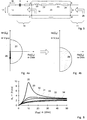
- For the electrical Conditions that arise at the coupling-in location of the bus coupling unit 14, can therefore represent the network in the form of a resulting network impedance 15 be (Figure 2b and 2c).
- This impedance 15 changes in amount and phase both over time by switching consumers on and off, as well as over the Location, i.e. e.g. at different sockets due to the changed composition the resulting impedance by different influence closer and more distant consumers and the different position of the connection point in the entire wiring topology of the specific installation.
- phase angle 0 ° ..90 °
- This different network impedance essentially determines according to FIG. 2c and FIG. 1 those from the transmitter amplifier via the RF transformer and the decoupling capacitor on the network, i.e. the resulting network impedance impressed transmission voltage 17 of the RF signals.
- the transformer 5 works primarily as an impedance converter, which is the network side Total impedance with the square of its ratio on the electronics side 11 transformed. Therefore, it can be used as a mathematical multiplier 22 for the network-side total impedance.
- the real im Components present in the coupling circuit are the leakage inductances 20, 23 and to consider the ohmic winding resistances 21, 24. Both and also that any fuse resistor 4 can be used temporarily to explain the operation be ignored.
- the transmission voltage 17 is dependent on the network impedance as follows.
- This impedance 26 of the decoupling capacitor can thus be represented as a point or vector in the complex plane with real and imaginary parts, as shown in FIG. 4a.
- the sum 28 of the network impedance and the impedance of the decoupling capacitor is important, which results from vectorial addition of the impedances according to FIG. 4b and results in a semicircle 28 shifted by X C 26.
- Each point on or within the shifted semicircle represents a possible resulting impedance at points A and A 'in FIGS. 1 and 3.
- the output voltage 9 at the transmission amplifier (FIG. 1) is a fixed value
- the magnitude of the transmission current is inversely proportional to Amount of the resulting impedance in the input circuit.
- FIG. 4b such points require a high transmission current that have a small amount, that is to say they are close to the zero point of the complex plane. This high current also generates a high transmission voltage U S or 17 over the resulting network impedance 15 from FIG. 2c.
- FIG. 5 shows the basic transmission voltages U S which are dependent on the network phase as a function of the amount of the network impedance Z network .
- the resulting impedance at points A, A 'or B, B' becomes greater than the actual network impedance if the network is ohmic or capacitive, since then the impedance pointers add up in the same way in the complex plane. This means that the resulting transmit voltage is even lower than it would be if the transmit amplifier were loaded directly with the pure network impedance.
- FIG. 5 shows an exemplary profile 29 of the transmission voltage on the network as Function of the amount of the network impedance at a phase angle of + 90 °, one Course 30 at a phase angle of + 60 °, course 31 at + 45 °, course 32 at 0 °, a course 33 at -45 ° and a course 34 at -90 °.
- At 35 is one Resonance point due to random compensation of the impedance of the decoupling capacitor designated by an inductive network.
- decoupling thus results in devices according to the prior art the mains voltage through a capacitor despite constant voltage at the output of the transmitter amplifier a phase and magnitude dependent Transmitting voltage for the RF signal or signals on the network node. Since the Mains impedance is not known, this technique leads to a non-reproducible Range of transmission signals that can go as far as loss of connection. On the other side in case of accidental compensation of the decoupling capacitor due to a phase inverse inductive network impedance, the transmission level is sometimes so high achieved that on the one hand long ranges are achieved, but on the other hand that associated transmit current peak the internal power supply of the bus coupling modules overloaded and thus the operating voltage of the devices collapses, resulting in Transmission aborts.
- the known technology leads to different ranges in capacitive and inductive networks, depending on the network phase position and the network impedance amount.
- the fourth point mentioned at the beginning relates to signal reception under presence of network-related faults.
- the actual receiving amplifier and the The type of signal evaluation depends on the modulation technique used, which is not the subject of the invention.
- the coupling circuit also decides about the effects of out-of-band disorders.
- the Decoupling capacitor not for additional suppression of high-frequency Interferences, because its impedance amount decreases with increasing frequency becomes.
- the invention is based on the object of specifying a bus coupling device, in which the transmission voltage impressed on the network is independent of the phase position the network impedance and as far as possible regardless of the amount the network impedance, i.e. is constant.
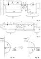
- FIG. 6 shows a bus coupling device according to the invention, which differs from the known shown in Fig. 1 bus coupling unit by a modified version of the Einkoppelnikes, which is designated in Fig. 6 at 16.
- the coupling circuit 16 contains a compensation inductor 36 which is in series with the fuse resistor 4 and the decoupling capacitor 3 is connected. With 5.1, 5.2 they are Primary or secondary winding of the transformer 5 referred to.
- the complex resistance of the coupling circuit 16 at the RF transmission frequency (eg 100 kHz) is almost zero, while the resistance of the compensation inductance at 50 Hz is negligible due to the much smaller frequency, so that the decoupling of the 230V remains unaffected.
- the galvanic isolation is also given by maintaining the transformer 5.
- the network impedance 15 from FIG. 2c results in a considerable advantage.
- the points A, A '(FIGS. 6 and 7) only the pure network impedance acts at the transmission frequency, since the complex components of the decoupling capacitor 3 and cancel the compensation inductance 36.
- the impedance at points A, A 'results from FIGS. 8a and 8b shifts slightly on the real axis. So that the network impedance is unaffected on RF transformer, and also transforms at the transmitter amplifier (points B, B '), effective.
- a second consideration concerns the dependence of the transmission voltage 17 on the amount the network impedance.
- the voltage drop is 17 over the resulting network impedance 15 (except for ohmic losses and transformer non-idealities) the only one in the coupling circuit (the voltage drops above the Decoupling capacitor and the compensation inductance compensate each other).
- This Transmit level 17 is equal to the transmit voltage transformed by the RF transmitter 9 at the amplifier output. This in turn is approximately constant if the Internal resistance of the RF transmitter 6 is lower than that transformed by the RF transmitter Is network impedance. This condition is only of the order of magnitude with network impedances from less than a few ohms. So that the transmission voltage 17 from one certain magnitude of the network impedance 15 even constant.
- the phase and partial magnitude independence of the transmission voltage 17 from the network impedance 15 is shown qualitatively in FIG. 9 and is shown by the comparison with the transmission voltage dependencies in the prior art in Figure 5 clearly.
- the proposed solution behaves like known devices because the Precompensation only changes the input impedance by a few ohms during the Transmitter the high-resistance input of reception stage 7 (a few kilo-ohms) in the Transformed input circuit and this value is still some 100 ohms. Pre-compensation therefore has practically no effect on reception behavior out.
- the series resonant circuit from decoupling capacitor 3 and compensation inductor 36 has the lowest at the RF transmission frequency Resistance.
- the impedance begins to increase as it increases is determined by the frequency-linear amount of the inductance.
- the series resonant circuit becomes capacitive, so that the frequencies are too small increasing amount of capacitor impedance becomes dominant. In this way out-of-band disturbances are effectively damped, so that the safety of the actual signal detection in the receiving part of the electronics is increased.
- the dimensioning of the compensation inductance mentioned above is exact for Systems that only work with an RF transmission frequency. This includes systems that work on the basis of amplitude modulation (ASK) and systems that use phase modulation Use (PSK). In the former, the information is in the change in amplitude, in the latter in the phase change of the same RF carrier signal.
- ASK amplitude modulation
- PSK phase modulation Use
- the impedance compensation can of course only be used for a frequency.
- the frequency spacing becomes practical through the transmission rate defines and lies in the range of a few kilohertz. This distance is in the sense the impedance compensation is close enough to the compensation inductance to tune the average transmission frequency without excessive residual impedances of the Compensating resonance circuit to receive at the transmission frequencies.
- This Residual impedances move e.g. with a frequency spacing of the transmission frequencies of 10 kHz and a center frequency of 110 kHz in the range of less than 1 Ohm.
- FIG. 10 Another embodiment of the invention could be pre-compensation also on the electronics side of the coupling circuit, i.e. on the secondary side of the transformer 5, as shown in Fig. 10.
- the 10 is the output of the transmission amplifier 6 below Interposition of a secondary-side inductor 45 with the secondary winding 5.2 of the transmitter 5 connected.
- the RF signal is transmitted via a coupling-out capacitor (in FIG. 10 not visible since part of the amplifier 6) is made free of DC voltage.
- This decoupling capacitor of course also has a distorting effect on the amplifier output effective total impedance of the coupling circuit in the sense of State of the art explanations. Compensation for this capacitor measures on the network side or vice versa is not possible, since the Precompensation by an inductive series connection must take place during the Capacitor through the transformer into a capacitance parallel to points A, A ' is transformed.
- the transmission voltage modulated onto the network for the RF carrier signals on the one hand, regardless of the phase position the network impedance and on the other hand also at higher network impedances regardless of the amount of network impedance.
- the transmission voltage can by an adaptation of the transmission amplifier can be adapted. This is a high probability for a homogeneous range of the network transmission system given in inductive and capacitive networks.
- a higher system stability is to be expected because of the overload of the power supply due to a too high transmission current only such network impedances are critical, which are close to 0 ohms.
- this case is essential less likely than the case that network impedances of the order of magnitude
- the impedance of the decoupling capacitor is (e.g. 10 ohms at 110 kHz and 0.15 ⁇ F Capacity) connected with inductive phase.
- a current limit Ensure stability in the transmitter amplifier.
- the participates the pre-compensation series resonant circuit positive for the damping of Out of band disorders.
Abstract
Description
Die Erfindung bezieht sich auf eine Buskoppeleinrichtung für ein Installationsbussystem mit Stromversorgungsnetz-gebundener Informationsübertragung unter Verwendung wenigstens eines HF-Trägersignals.The invention relates to a bus coupling device for an installation bus system with power grid-bound information transmission using at least one RF carrier signal.
Bei der netzgebundenen Übertragungstechnik wird das 230V/50Hz-Stromversorgungsnetz, oder ein anderes, z.B. 110V/60Hz-Netz, zusätzlich zu seiner herkömmlichen Stromversorgungsfunktion als Bussystem für die Übertragung von Informationen benutzt. Eine solche Technik wird im Rahmen der Gebäudeautomatisierung als Installationsbussystem zur flexiblen logischen Zuordnung von Sensoren (Schalter, Temperaturfühler, Windmesser, Steuergeräte) zu Aktoren (Dimmer, Heizungen, Jalousien etc.) eingesetzt. Die Übertragung solcher Steuerfunktionen auf dem Stromnetz als physikalisches Medium ist dabei für viele Anwender eine besonders kostengünstige Lösung im Vergleich zu anderen Installationsbussystemen, die separate Übertragungsmedien, wie z.B. Zweidrahtleitung (twisted pair) beim Europäischen Installationsbus (EIB) oder Glasfaserkabel benutzen. Letztere erfordern eine zum Stromversorgungsnetz parallelgeführte Installation eines zweiten Kabels. With the network-based transmission technology, the 230V / 50Hz power supply network, or another, e.g. 110V / 60Hz network, in addition to its conventional Power supply function as a bus system for the transmission of information used. Such a technology is used as part of building automation Installation bus system for flexible logical assignment of sensors (switches, Temperature sensors, anemometers, control devices) for actuators (dimmers, heaters, blinds etc.) used. The transfer of such control functions on the power grid As a physical medium, many users find it particularly cost-effective Solution compared to other installation bus systems, the separate Transmission media, e.g. Two-wire cable (twisted pair) in the European Use installation bus (EIB) or fiber optic cable. The latter require one to Power supply network Installation of a second cable in parallel.
Dieser Vorteil wird erkauft durch die gemeinsame Nutzung der Stromversorgungsleitung mit den damit verbundenen Nachteilen, die durch Netzstörungen und schwankende Güte des Übertragungskanals für die Nutzinformationen entstehen können. Die Nutzinformation selbst wird dabei in einem von der 50Hz-Versorgungsfrequenz abweichenden Frequenzbereich übertragen. In Europa steht dafür auf der Verbraucherseite, also in Gebäuden, z.B. der Bereich von 95..148,5 KHz zur Verfügung. Energieversorgungsunternehmen nutzen in Europa den Bereich von 3...95 kHz.This advantage is paid for by sharing the power supply line with the associated disadvantages caused by network disturbances and fluctuating Quality of the transmission channel for which useful information can arise. The useful information itself is in one of the 50 Hz supply frequency deviating frequency range. In Europe, on the consumer side, i.e. in buildings, e.g. the range of 95..148.5 KHz is available. Power supply companies in Europe use the 3 ... 95 kHz range.
Die Informationen wiederum werden in geeigneter Weise kodiert und in Form von
modulierten Trägerfrequenzen als HF-Signale übertragen. Hier kommen bekannte
Verfahren, wie Amplitudenumtastung (engl.: amplitude shift keying = ASK), Frequenzumtastung
mit und ohne Bandspreizung (engl.: frequency shift keying = FSK) und
Phasenumtastung (eng.: phase shift keying = PSK) zur Anwendung. Solche Netzbussysteme
sind von verschiedenen Herstellern bekannt. In der Druckschrift ![]()
![]()
Die Schnittstelle zwischen einer "Anwendung" (Sensor oder Aktor) und dem "Bus" (230V-Stromversorgungsleitung) wird in Netzbussystemen durch sogenannte Buskoppelbausteine (engl.: bus coupling unit = BCU) hergestellt. Diese Buskoppelbausteine erfüllen die Sende- und Empfangsfunktionen des Netzübertragungssystems. Dabei muß den Besonderheiten Rechnung getragen werden, die durch die 230V-Stromversorgungsleitung als Bus gegeben sind. Dazu gehören in erster Linie die Notwendigkeit der galvanischen Trennung zwischen Bus und Applikation, zweitens das Problem der variierenden Impedanz des jeweiligen Punktes im Versorgungsnetz, an dem der Buskoppelbaustein angeschlossen ist, drittens die damit verbundenen Unterschiede im auf das Netz aufgeprägten Sendepegel und der damit verbundenen Sendereichweite und viertens der Signalempfang unter Präsenz verschiedener Netzstörungen im Sendefrequenzband, wie z. B. Surge- und Burst-Impulse sowie verschiedene Formen des Rauschens.The interface between an "application" (sensor or actuator) and the "bus" (230V power supply line) in network bus systems through so-called bus coupling modules (English: bus coupling unit = BCU). These bus coupling modules perform the send and receive functions of the network transmission system. The peculiarities that are caused by the 230V power supply line are provided as a bus. This primarily includes second, the need for electrical isolation between the bus and the application the problem of the varying impedance of the respective point in the supply network, third to which the bus coupling module is connected associated differences in the transmission level impressed on the network and the associated connected transmission range and fourth the signal reception in the presence of different Network interference in the transmission frequency band, such as. B. Surge and burst pulses as well as various forms of noise.
Eine typische Schaltungsanordnung einer Buskoppeleinheit gemäß dem Stand der Technik ist in Fig. 1 dargestellt.A typical circuit arrangement of a bus coupling unit according to the prior art Technique is shown in Fig. 1.
In Fig. 1 ist der Nulleiter einer 230V/50Hz-Stromversorgungsleitung mit 1 bezeichnet,
der zugehörige Phasenleiter mit 2. Zur galvanischen Trennung ist ein
HF-Übertrager 5 mit primären Anschlußpunkten A, A' und sekundären Anschlußpunkten
B, B' angeordnet.In Fig. 1, the neutral conductor of a 230V / 50Hz power supply line is designated 1,
the associated phase conductor with 2. For galvanic isolation is a
Der HF-Übertrager 5 im Eingangskreis fungiert bidirektional für den Abgriff von
Empfangsinformationen und für die Netzaufprägung von Sendeinformation. Insbesondere
muß der Übertrager 5 für die verwendeten Trägerfrequenzen optimiert werden,
was einen direkten Betrieb am 230V-Netz aus Impedanz- und Verlustleistungsgründen
ausschließt.The
Um die 230V bei 50Hz vom HF-Übertrager 5 zu isolieren, ist deshalb zwischen den
Anschluß A der netzseitigen Wicklung des Übertragers 5 und die Phase 2 des
Stromnetzes ein Entkoppelkondensator 3 geschaltet, der für die relativ niedrige Versorgungsfrequenz
von 50Hz einen hohen Betrag seiner Impedanz besitzt, während
er für die viel höheren Sendefrequenzen im Bereich um 100kHz einen sehr geringen
Widerstand aufweist, um das Sendesignal nicht auch zu dämpfen. Der zweite Anschluß
der netzseitigen Übertragerwicklung ist direkt mit dem Nulleiter 1 des Netzes
verbunden. Zusätzlich kann mit dem Kondensator 3 ein Sicherungswiderstand 4 in
Reihe liegen, der z.B. in Europa normativ erforderlich ist, einen Widerstandswert von
ca. < 0,1 Ohm besitzt und keine für die Übertragung relevante Bedeutung besitzt.To isolate the 230V at 50Hz from the
Der auf den Übertrager 5 bezogene netzseitige Teil des Buskoppeleinrichtung ist in
Fig. 1 mit 10 bezeichnet, eine Elektronikseite bildender Teil ist mit 11 bezeichnet.
Die Elektronikseite 11 enthält einen Sendeverstärker 6, einen Empfangsverstärker 7
und eine Steuerlogik 8.The network-side part of the bus coupling device related to the
Das zweite Problem, nämlich die unbekannte Netzimpedanz, ist zwar aus einigen
wenigen veröffentlichten Untersuchungen bekannt, wurde aber bisher bei der Auslegung
der Buskoppeleinrichtung nicht berücksichtigt. Wesentlich ist die Tatsache,
daß die Reichweite von Netzbussignalen (o.g. Punkt 3) unter anderem davon abhängt,
welcher Sendepegel bzw. welche Sendespannung 17 (Fig. 1) am Ort des
Senders auf das Netz aufgeprägt werden kann. Da das Netz signaldämpfend wirkt,
ist eine hohe Sendespannung die Voraussetzung für eine hohe Reichweite, also
eine große überbrückbare Kabellänge. Die erreichbare Sendespannung ist aber davon
abhängig, welche Netzimpedanz nach Betrag und Phase von der Buskoppeleinheit
am Ort ihrer Netzanschaltung gesehen wird.The second problem, namely the unknown grid impedance, is due to some
few published studies known, but has so far been interpreted
the bus coupling device is not taken into account. What is essential is
that the range of network bus signals (
Diese resultierende Netzimpedanz entsteht aus der gemeinsamen Wirkung aller am
Netz angeschlossenen Verbraucher, inklusive der von den Netzkabeln selbst dargestellten
Impedanz am Ort der Anschaltung der Buskoppeleinheit (BCU). Dies wird
anhand der Fig. 2a, 2b und 2c verdeutlicht, worin angeschlossene Verbraucher, z.B.
eine Beleuchtung mit 12, und ein Fernsehgerät mit 13 bezeichnet sind. Für die elektrischen
Verhältnisse, die sich am Einkoppelort der Buskoppeleinheit 14 ergeben,
kann deshalb das Netz in Form einer resultierenden Netzimpedanz 15 dargestellt
werden (Figur 2b und 2c). Diese Impedanz 15 ändert sich in Betrag und Phase sowohl
über die Zeit durch Ab- und Zuschalten von Verbrauchern, als auch über den
Ort, d.h. z.B. an unterschiedlichen Steckdosen, infolge der geänderten Zusammensetzung
der resultierenden Impedanz durch unterschiedlichen Einfluß näher und
entfernter liegender Verbraucher sowie die unterschiedliche Position der Anschlußstelle
in der gesamten Verdrahtungstopologie der konkreten Installation.This resulting network impedance arises from the common effect of all am
Connected consumers, including those represented by the power cables themselves
Impedance at the point of connection of the bus coupling unit (BCU). this will
2a, 2b and 2c illustrates in which connected consumers, e.g.
a lighting with 12, and a television set with 13 are designated. For the electrical
Conditions that arise at the coupling-in location of the
Möglich sind deshalb der Phase nach induktive (Phasenwinkel = 0°..90°) und kapazitive (Phasenwinkel = -90°..0°) Netze mit Impedanzen, die sich betragsmäßig vorwiegend im Wertebereich von 0..50 Ohm befinden.Inductive (phase angle = 0 ° ..90 °) and capacitive are therefore possible (Phase angle = -90 ° ..0 °) networks with impedances that vary in amount predominantly in the range of 0..50 Ohm.
Diese unterschiedliche Netzimpedanz bestimmt nach Figur 2c und Figur 1 wesentlich
die vom Sendeverstärker über den HF-Übertrager und den Entkoppelkondensator
auf das Netz, d.h. die resultierende Netzimpedanz aufgeprägte Sendespannung
17 der HF-Signale.This different network impedance essentially determines according to FIG. 2c and FIG. 1
those from the transmitter amplifier via the RF transformer and the decoupling capacitor
on the network, i.e. the resulting network impedance impressed
Gründe sind die endliche Sendeleistung des Sendeverstärkers 6 und der bei konstanter
Sendespannung 9 am Verstärkerausgang (Figur 1) unterschiedliche netzimpedanzabhängige
Sendestrom 18 durch die Netzimpedanz.The reasons are the finite transmission power of the
Eine weitere Erläuterung der Impedanzverhältnisse erfolgt nachstehend anhand der
Fig. 3, in der der Übertrager 5 durch ein Ersatzschaltbild nachgebildet ist.A further explanation of the impedance relationships is given below using the
Fig. 3, in which the
Der Übertrager 5 arbeitet in erster Linie als Impedanzkonverter, der die netzseitige
Gesamtimpedanz mit dem Quadrat seines Übersetzungsverhältnisses auf die Elektronikseite
11 transformiert. Deswegen kann er als mathematischer Multiplikator 22
für die netzseitige Gesamtimpedanz angesehen werden. Zusätzlich zu den real im
Einkoppelkreis vorhandenen Bauelementen sind noch die Streuinduktivitäten 20, 23
und die ohmschen Wicklungswiderstände 21, 24 zu betrachten. Beide und auch der
eventuelle Sicherungswiderstand 4 können für die Erklärung der Arbeitsweise vorübergehend
vernachlässigt werden.The
Bei Anordnungen gemäß dem Stand der Technik (Figur 1) ist die Sendespannung
17 wie folgt von der Netzimpedanz abhängig. Der Entkoppelkondensator 3 besitzt
einen Betrag, der durch
Diese Sendespannung ist also genau dann maximal, wenn die Netzimpedanz denselben
Betrag aufweist, wie die Impedanz des Entkoppelkondensators, d.h.
Figur 5 zeigt die prinzipiellen, von der Netzphase abhängigen Sendespannungen US als Funktion des Betrages der Netzimpedanz ZNetz. Insbesondere wird die resultierende Impedanz an den Punkten A,A' bzw. B,B' größer als die eigentliche Netzimpedanz, wenn das Netz ohmsch oder kapazitiv ist, da sich dann die Impedanzzeiger in der komplexen Ebene gleichsinnig addieren. Damit ist die resultierende Sendespannung sogar kleiner, als sie bei direkter Belastung des Sendeverstärkers mit der reinen Netzimpedanz wäre. FIG. 5 shows the basic transmission voltages U S which are dependent on the network phase as a function of the amount of the network impedance Z network . In particular, the resulting impedance at points A, A 'or B, B' becomes greater than the actual network impedance if the network is ohmic or capacitive, since then the impedance pointers add up in the same way in the complex plane. This means that the resulting transmit voltage is even lower than it would be if the transmit amplifier were loaded directly with the pure network impedance.
Fig. 5 zeigt einen beispielhaften Verlauf 29 der Sendespannung auf dem Netz als
Funktion des Betrages der Netzimpedanz bei einem Phasenwinkel von +90°, einen
Verlauf 30 bei einem Phasenwinkel von +60°, einen Verlauf 31 bei +45°, einen Verlauf
32 bei 0°, einen Verlauf 33 bei -45° und einen Verlauf 34 bei -90°. Mit 35 ist eine
Resonanzstelle auf Grund zufälliger Kompensation der Impedanz des Entkoppelkondensators
durch ein induktives Netz bezeichnet.FIG. 5 shows an
Zusammenfassend bewirkt also bei Geräten gemäß dem Stand der Technik die Entkopplung der Netzspannung durch einen Kondensator trotz konstanter Spannung am Ausgang des Sendeverstärkers eine von der Phase und vom Betrag stark abhängige Sendespannung für das oder die HF-Signale auf dem Netzknoten. Da die Netzimpedanz nicht bekannt ist, führt diese Technik zu einer nicht reproduzierbaren Reichweite von Sendesignalen, die bis zum Verbindungsverlust gehen kann. Auf der anderen Seite werden im Falle der zufälligen Kompensation des Entkoppelkondensators durch eine phaseninverse induktive Netzimpedanz partiell so hohe Sendepegel erreicht, daß einerseits hohe Reichweiten erzielt werden, aber andererseits die damit verbundene Sendestromspitze das interne Netzteil der Buskoppelbausteine überlastet und damit die Betriebsspannung der Geräte zusammenbricht, was zum Übertragungsabbruch führt.In summary, decoupling thus results in devices according to the prior art the mains voltage through a capacitor despite constant voltage at the output of the transmitter amplifier a phase and magnitude dependent Transmitting voltage for the RF signal or signals on the network node. Since the Mains impedance is not known, this technique leads to a non-reproducible Range of transmission signals that can go as far as loss of connection. On the other side in case of accidental compensation of the decoupling capacitor due to a phase inverse inductive network impedance, the transmission level is sometimes so high achieved that on the one hand long ranges are achieved, but on the other hand that associated transmit current peak the internal power supply of the bus coupling modules overloaded and thus the operating voltage of the devices collapses, resulting in Transmission aborts.
Die bekannte Technik führt damit zu unterschiedlichen Reichweiten in kapazitiven und induktiven Netzten, abhängig von der Netzphasenlage und dem Netzimpedanzbetrag.The known technology leads to different ranges in capacitive and inductive networks, depending on the network phase position and the network impedance amount.
Der eingangs genannte vierte Punkt bezieht sich auf den Signalempfang unter Präsenz von netzgebundenen Störungen. Der eigentliche Empfangsverstärker und die Art der Signalauswertung sind abhängig von der verwendeten Modulationstechnik, die nicht Gegenstand der Erfindung ist. Allerdings entscheidet auch die Einkoppelschaltung über die Wirkungen von Außerbandstörungen. In dieser Hinsicht trägt der Entkoppelkondensator nicht zur zusätzlichen Unterdrückung von hochfrequenten Störungen bei, da sein Impedanz-Betrag mit steigender Frequenz immer geringer wird.The fourth point mentioned at the beginning relates to signal reception under presence of network-related faults. The actual receiving amplifier and the The type of signal evaluation depends on the modulation technique used, which is not the subject of the invention. However, the coupling circuit also decides about the effects of out-of-band disorders. In this regard, the Decoupling capacitor not for additional suppression of high-frequency Interferences, because its impedance amount decreases with increasing frequency becomes.
Der Erfindung liegt die Aufgabe zugrunde, eine Buskoppeleinrichtung anzugeben, bei der die auf das Netz aufgeprägte Sendespannung unabhängig von der Phasenlage der Netzimpedanz und soweit wie möglich auch unabhängig von dem Betrag der Netzimpedanz, d.h. konstant ist.The invention is based on the object of specifying a bus coupling device, in which the transmission voltage impressed on the network is independent of the phase position the network impedance and as far as possible regardless of the amount the network impedance, i.e. is constant.
Gleichzeitig sollen die galvanische Isolation und die Empfangsempfindlichkeit der Buskoppeleinrichtung und der daran angeschlossenen Geräte unbeeinflußt bleiben. Wenn möglich soll sogar eine verbesserte Unterdrückung von Störsignalen außerhalb des Nutzfrequenzbandes der HF-Signale erreicht werden. Damit würde eine Technik existieren, mit der die Übertragungseigenschaften des netzgebundenen Installationsbussystems unabhängig von der sich zeitlich und örtlich ändernden Netzimpedanz konstant und auf vorherbestimmbarem Qualitätsniveau gehalten werden könnten. Das System würde in stark induktiven Netzen genauso sicher arbeiten und ähnliche Reichweiten erzielen, wie in schwach induktiven oder gar kapazitiven Netzen.At the same time, the galvanic isolation and the reception sensitivity of the Bus coupling device and the devices connected to it remain unaffected. If possible, even improved suppression of interference signals outside of the useful frequency band of the RF signals can be reached. That would make one Technology exist with which the transmission properties of the network-connected installation bus system regardless of the changing time and place Mains impedance can be kept constant and at a predeterminable quality level could. The system would work just as safely in highly inductive networks and achieve similar ranges as in weakly inductive or even capacitive Nets.
Diese Aufgabe wird durch eine Buskoppeleinrichtung mit den im Anspruch 1 angegebenen
Merkmalen gelöst. Vorteilhafte Ausgestaltungen sind in weiteren Ansprüchen
angegeben. This object is achieved by a bus coupling device with the specified in
Es wird vorgeschlagen, im Einkoppelkreis eines Buskoppelbausteines eine zusätzliche Induktivität in Serie zum Entkoppelkondensator zu schalten, die eine interne Vorkompensation der geräteeigenen Eingangsimpedanz bewirkt. Die Induktivität wird so berechnet, daß die Impedanz der Induktivität bei der Frequenz des HF-Trägersignals genau die Impedanz des Entkoppelkondensators kompensiert. Falls mehrere verschiedene Trägerfrequenzen zum Einsatz kommen, erfolgt die Dimensionierung wie weiter unten angegeben. Damit ist im Eingangskreis durch den für die HF-Sendefrequenz bewußt erzeugten Serienresonanzkreis nur noch der ohmsche Wicklungswiderstand der "Kompensationsinduktivität" wirksam, der im Milliohmbereich liegt und für die Funktion vernachlässigbar ist.It is proposed to add an additional one in the coupling circuit of a bus coupling module To connect inductance in series to the decoupling capacitor, which is an internal Precompensation of the device's own input impedance. The inductance is calculated so that the impedance of the inductance at the frequency of the RF carrier signal exactly the impedance of the decoupling capacitor is compensated. If If several different carrier frequencies are used, the dimensioning takes place as indicated below. This is in the input circuit by the for the HF transmission frequency deliberately created series resonance circuit only the ohmic Winding resistance of the "compensation inductance" effective, that in the milliohm range lies and is negligible for the function.
Eine weitere Erläuterung der Erfindung und ihrer Vorteile erfolgt anhand der Zeichnungsfiguren. A further explanation of the invention and its advantages is given on the basis of the drawing figures.
Es zeigen:
- Fig. 1
- eine Buskoppeleinheit gemäß dem Stand der Technik,
- Fig. 2a, 2b, 2c
- Darstellungen zur Erläuterung der Entstehung einer resultierenden Netzimpedanz am Ort der Anschaltung einer Buskoppeleinheit,
- Fig. 3
- ein Ersatzschaltbild zur Anordnung gemäß Fig. 1,
- Fig. 4a, 4b
- vektorielle Darstellungen von Impedanzen,
- Fig. 5
- Verläufe von Sendespannungen, bezogen auf den Stand der Technik,
- Fig. 6
- eine erfindungsgemäße Buskoppeleinrichtung,
- Fig. 7
- ein Ersatzschaltbild zur Anordnung gemäß Fig. 6,
- Fig. 8a, 8b
- vektorielle Darstellungen von Impedanzen,
- Fig. 9
- eine Darstellung der Abhängigkeit der Sendespannung von der Netzimpedanz, bezogen auf die erfindungsgemäße Buskoppeleinheit mit Vorkompensation, und
- Fig. 10
- eine Erweiterung der in Fig. 6 gezeigten Buskoppeleinrichtung durch eine sekundärseitige Vorkompensation.
- Fig. 1
- a bus coupling unit according to the prior art,
- 2a, 2b, 2c
- Representations to explain the formation of a resulting network impedance at the point of connection of a bus coupling unit,
- Fig. 3
- 2 shows an equivalent circuit diagram for the arrangement according to FIG. 1,
- 4a, 4b
- vector representations of impedances,
- Fig. 5
- Curves of transmission voltages, based on the state of the art,
- Fig. 6
- a bus coupling device according to the invention,
- Fig. 7
- 6 shows an equivalent circuit diagram for the arrangement according to FIG. 6,
- 8a, 8b
- vector representations of impedances,
- Fig. 9
- a representation of the dependence of the transmission voltage on the network impedance, based on the bus coupling unit according to the invention with pre-compensation, and
- Fig. 10
- an expansion of the bus coupling device shown in Fig. 6 by a secondary pre-compensation.
Fig. 6 zeigt eine erfindungsgemäße Buskoppeleinrichtung, die sich von der bekannten,
in Fig. 1 dargestellten Buskoppeleinheit durch eine geänderte Ausführung des
Einkoppelkreises unterscheidet, der in Fig. 6 mit 16 bezeichnet ist. Der Einkoppelkreis
16 enthält eine Kompensationsinduktivität 36, die in Serie zum Sicherungswiderstand
4 und dem Entkopplungskondensator 3 geschaltet ist. Mit 5.1, 5.2 sind die
Primär- bzw. Sekundärwicklung des Übertragers 5 bezeichnet. 6 shows a bus coupling device according to the invention, which differs from the known
shown in Fig. 1 bus coupling unit by a modified version of the
Einkoppelkreises, which is designated in Fig. 6 at 16. The
Die Dimensionierung der Kompensationsinduktivität 36 erfolgt durch Gleichsetzung
des kapazitiven Widerstandes und der induktiven Widerstände im Ersatzschaltbild,
das Fig. 7 zeigt und dessen Bezugszeichen die gleiche Bedeutung haben wie bei
Fig. 3. Falls die Streuinduktivitäten vernachlässigbar sind, gilt
Für die resultierende Impedanz 19 des Einkoppelkreises 16 unter Berücksichtigung
der Netzimpedanz 15 aus Figur 2c ergibt sich ein erheblicher Vorteil. An den Punkten
A,A' (Fig. 6 und 7) wirkt bei der Sendefrequenz nur noch die reine Netzimpedanz,
da sich bei dieser Frequenz die komplexen Anteile des Entkoppelkondensators
3 und der Kompensationsinduktivität 36 aufheben. Unter Berücksichtigung der
geringen ohmschen Restwiderstände (ohmsche Anteile der Kompensationsinduktivität
36 und der Übertragerwicklungen 5.1, 5.2 sowie eventuell des Sicherungswiderstandes
4) ergibt sich die Impedanz an den Punkten A,A' nach den Figuren 8a und
8b. Der Halbkreis, der die möglichen Netzimpedanzen beschreibt, verschiebt sich
geringfügig auf der reellen Achse. Damit wird die Netzimpedanz unbeeinflußt am
HF-Übertrager, und transformiert auch am Sendeverstärker (Punkte B,B'), wirksam.Taking into account the resulting
Damit hängt bei konstanter HF-Ausgangsspannung 9 am Sendeverstärker 6 (Fig. 6)
der Sendestrom 18 direkt vom Betrag der Netzimpedanz ab und nicht von geräteinternen
frequenzabhängigen Bauelementen. Insbesondere spielt es keine Rolle, ob
das Netz kapazitiv oder induktiv ist, denn die resultierende Zeigerlänge in Figur 8b
ist für alle Netzphasenlagen mit jeweils gleichem Betrag bis auf den vernachlässigbaren
Einfluß der ohmschen Restwiderstände gleich lang. Damit ist auch die auf das
Netz aufgeprägte Sendespannung 17 unabhängig von der Phasenlage der Netzimpedanz
15, womit eine wesentliche Forderung der Aufgabenstellung erfüllt ist.With constant
Eine zweite Überlegung betrifft die Abhängigkeit der Sendespannung 17 vom Betrag
der Netzimpedanz. Bei der vorgeschlagenen Lösung ist der Spannungsabfall 17
über der resultierenden Netzimpedanz 15 (bis auf ohmsche Verluste und Übertragernichtidealitäten)
der einzige im Einkoppelkreis (die Spannungsabfälle über dem
Entkoppelkondensator und der Kompensationsinduktivität kompensieren sich). Dieser
Sendepegel 17 ist gleich der vom HF-Übertrager transformierten Sendespannung
9 am Verstärkerausgang. Diese wiederum ist annähernd konstant, wenn der
Innenwiderstand des HF-Senders 6 kleiner als die vom HF-Übertrager transformierte
Netzimpedanz ist. Diese Bedingung wird erst bei Netzimpedanzen in der Größenordnung
von kleiner einiger Ohm verlassen. Damit ist die Sendespannung 17 ab einer
bestimmten Betragsgröße der Netzimpedanz 15 sogar konstant.
Die Phasen- und die partielle Betragsunabhängigkeit der Sendespannung 17 von
der Netzimpedanz 15 ist qualitativ in Fig. 9 dargestellt und wird durch den Vergleich
mit den Sendespannungsabhängigkeiten beim Stand der Technik in Figur 5 deutlich.A second consideration concerns the dependence of the
Bezüglich des Empfangsverhaltens und der Eingangsimpedanz der Buskoppeleinrichtung verhält sich die vorgeschlagene Lösung wie bekannte Einrichtungen, da die Vorkompensation die Eingangsimpedanz nur um einige Ohm ändert, während der Übertrager den hochohmigen Eingang der Empfangsstufe 7 (einige Kilo-Ohm) in den Eingangskreis transformiert und dieser Wert immer noch einige 100 Ohm beträgt. Damit wirkt sich die Vorkompensation praktisch nicht auf das Empfangsverhalten aus.Regarding the reception behavior and the input impedance of the bus coupling device the proposed solution behaves like known devices because the Precompensation only changes the input impedance by a few ohms during the Transmitter the high-resistance input of reception stage 7 (a few kilo-ohms) in the Transformed input circuit and this value is still some 100 ohms. Pre-compensation therefore has practically no effect on reception behavior out.
Andererseits ist die vorgestellte Lösung vorteilhaft hinsichtlich der Unterdrückung
hochfrequenter Netzstörungen. Der Serienschwingkreis aus Entkoppelkondensator 3
und Kompensationsinduktivität 36 besitzt bei der HF-Sendefrequenz den geringsten
Widerstand. Für höhere Frequenzen beginnt die Impedanz zu steigen, da sie zunehmend
von dem frequenzlinearen Betrag der Induktivität bestimmt wird. Für kleinere
Frequenzen wird der Serienschwingkreis kapazitiv, so daß der zu kleinen Frequenzen
steigende Betrag der Kondensatorimpedanz dominant wird. Auf diese Weise
werden Außerbandstörungen wirksam vorgedämpft, so daß die Sicherheit der
eigentlichen Signalerkennung im Empfangsteil der Elektronik erhöht wird.On the other hand, the solution presented is advantageous in terms of suppression
high-frequency network interference. The series resonant circuit from
Die bisher genannte Dimensionierung der Kompensationsinduktivität ist exakt für Systeme, die nur mit einer HF-Sendefrequenz arbeiten. Dazu zählen Systeme, die auf der Basis der Amplitudenmodulation (ASK) arbeiten und Systeme, die die Phasenmodulation (PSK) verwenden. Bei ersteren steckt die Information in der Amplitudenänderung, bei letzteren in der Phasenänderung desselben HF-Trägersignals.The dimensioning of the compensation inductance mentioned above is exact for Systems that only work with an RF transmission frequency. This includes systems that work on the basis of amplitude modulation (ASK) and systems that use phase modulation Use (PSK). In the former, the information is in the change in amplitude, in the latter in the phase change of the same RF carrier signal.
Bei Systemen auf der Basis der Frequenzmodulation (FSK) wird die Information in Form von Frequenzänderungen übermittelt, d.h. es gibt mehr als nur eine HF-Trägerfrequenz. In diesem Fall kann die Impedanzkompensation natürlich nur für eine Frequenz erfolgen. Praktisch wird der Frequenzabstand durch die Übertragungsrate definiert und liegt im Bereich einiger Kilohertz. Dieser Abstand ist im Sinne der Impedanzkompensation dicht genug, um die Kompensationsinduktivität auf die mittlere Sendefrequenz abzustimmen, ohne dabei zu große Restimpedanzen des Kompensationsschwingkreises bei den Sendefrequenzen zu erhalten. Diese Restimpedanzen bewegen sich z.B. bei einem Frequenzabstand der Sendefrequenzen von 10KHz und einer Mittenfrequenz von 110 KHz im Bereich von kleiner 1 Ohm.In systems based on frequency modulation (FSK), the information in Form of frequency changes transmitted, i.e. there is more than one RF carrier frequency. In this case the impedance compensation can of course only be used for a frequency. The frequency spacing becomes practical through the transmission rate defines and lies in the range of a few kilohertz. This distance is in the sense the impedance compensation is close enough to the compensation inductance to tune the average transmission frequency without excessive residual impedances of the Compensating resonance circuit to receive at the transmission frequencies. This Residual impedances move e.g. with a frequency spacing of the transmission frequencies of 10 kHz and a center frequency of 110 kHz in the range of less than 1 Ohm.
Eine weitere erfindungsgemäße Ausbildung könnte darin liegen, die Vorkompensation
auch zusätzlich auf der Elektronikseite der Einkoppelschaltung, also auf der Sekundärseite
des Übertragers 5 vorzusehen, wie in Fig. 10 dargestellt ist. In der
Schaltungsanordnung gemäß Fig. 10 ist der Ausgang des Sendeverstärkers 6 unter
Zwischenschaltung einer sekundärseitigen Induktivität 45 mit der Sekundärwicklung
5.2 des Übertragers 5 verbunden. Dies wird z.B. interessant, wenn der Ausgang des
Sendeverstärkers 6 gegenüber der Schaltungsmasse nicht gleichspannungsfrei ist.
In diesen Fällen wird das HF-Signal über einen Auskoppelkondensator (in Fig. 10
nicht sichtbar, da Teil des Verstärkers 6) gleichspannungsfrei gemacht. Dieser Auskoppelkondensator
wirkt natürlich ebenfalls verzerrend bezüglich der für den Verstärkerausgang
wirksamen Gesamtimpedanz des Einkoppelkreises im Sinne der
Erläuterungen zum Stand der Technik. Eine Kompensation dieses Kondensators
durch Maßnahmen auf der Netzseite oder umgekehrt ist dabei nicht möglich, da die
Vorkompensation durch eine induktive Reihenschaltung erfolgen muß, während der
Kondensator durch den Übertrager in eine zu den Punkten A,A' parallele Kapazität
transformiert wird.Another embodiment of the invention could be pre-compensation
also on the electronics side of the coupling circuit, i.e. on the secondary side
of the
Zusammenfassend ist also festzustellen, daß durch die interne Impedanzvorkompensation aller komplexen Widerstände im Einkoppelkreis von Buskoppelbausteinen für die netzgebundene Übertragungstechnik die auf das Netz aufmodulierte Sendespannung für die HF-Trägersignale zum einen unabhängig von der Phasenlage der Netzimpedanz und zum anderen zumindest bei höheren Netzimpedanzen auch unabhängig vom Betrag der Netzimpedanz wird. Die Sendespannung kann durch eine Anpassung des Sendeverstärkers adaptiert werden. Damit ist eine hohe Wahrscheinlichkeit für eine homogene Reichweite des netzgebundenen Übertragungssystems in induktiven und kapazitiven Netzen gegeben.In summary, it should be noted that the internal impedance pre-compensation of all complex resistors in the coupling circuit of bus coupling modules for the network-based transmission technology, the transmission voltage modulated onto the network for the RF carrier signals, on the one hand, regardless of the phase position the network impedance and on the other hand also at higher network impedances regardless of the amount of network impedance. The transmission voltage can by an adaptation of the transmission amplifier can be adapted. This is a high probability for a homogeneous range of the network transmission system given in inductive and capacitive networks.
Weiterhin ist eine höhere Systemstabilität zu erwarten, da bezüglich der Überlastung des Netzteils durch einen zu hohen Sendestrom nur noch solche Netzimpedanzen kritisch sind, die betragsmäßig nahe 0 Ohm liegen. Dieser Fall ist jedoch wesentlich unwahrscheinlicher als der Fall, daß Netzimpedanzen in der Größenordnung der Impedanz des Entkoppelkondensators liegen (z.B. 10 Ohm bei 110 kHz und 0,15 µF Kapazität), verbunden mit induktiver Phasenlage. In jedem Fall kann eine Strombegrenzung im Sendeverstärker die Stabilität sichern. Darüber hinaus wirkt sich der mit der Vorkompensation entstehende Serienschwingkreis positiv auf die Dämpfung von Außerbandstörungen aus. Furthermore, a higher system stability is to be expected because of the overload of the power supply due to a too high transmission current only such network impedances are critical, which are close to 0 ohms. However, this case is essential less likely than the case that network impedances of the order of magnitude The impedance of the decoupling capacitor is (e.g. 10 ohms at 110 kHz and 0.15 µF Capacity) connected with inductive phase. In any case, a current limit Ensure stability in the transmitter amplifier. In addition, the participates the pre-compensation series resonant circuit positive for the damping of Out of band disorders.
- 11
- Nulleiter der 230V/50Hz StromversorgungsleitungNeutral conductor of the 230V / 50Hz power supply line
- 22nd
- Phase der 230V/50Hz StromversorgungsleitungPhase of the 230V / 50Hz power supply line
- 33rd
- EntkoppelkondensatorDecoupling capacitor
- 44th
- SicherungswiderstandFuse resistor
- 55
- HF-ÜbertragerRF transmitter
- 5.15.1
- PrimärwicklungPrimary winding
- 5.25.2
- SekundärwicklungSecondary winding
- 66
- SendeverstärkerTransmitter amplifier
- 77
- EmpfangsverstärkerReception amplifier
- 88th
- SteuerlogikControl logic
- 99
- Sendespannung am Ausgang des SendeverstärkersTransmission voltage at the output of the transmission amplifier
- 1010th
- Netzseite des Buskoppelbausteines bezogen auf den HF-Übertrager als galvanische TrennungNetwork side of the bus coupling module with respect to the HF transformer as galvanic separation
- 1111
- Elektronikseite des Buskoppelbausteines bezogen auf den HF-Übertrager als galvanische TrennungElectronics side of the bus coupling module related to the RF transmitter as galvanic isolation
- 1212th
- Verbraucher, z.B. BeleuchtungConsumers, e.g. lighting
- 1313
- Verbraucher, z.B. FernseherConsumers, e.g. TV
- 1414
- BuskoppelbausteinBus coupling module
- 1515
- resultierende Netzimpedanz am Ort der Netzankopplung eines Buskoppelbausteinesresulting network impedance at the location of the network connection of a bus coupling module
- 1616
- EinkoppelkreisCoupling circuit
- 1717th
- Sendespannung über der resultierenden NetzimpedanzTransmitting voltage over the resulting network impedance
- 1818th
- SendestromTransmission current
- 1919th
- resultierende Eingangsimpedanz für den HF-Übertrager auf der Netzseiteresulting input impedance for the RF transmitter on the network side
- 2020th
- netzseitige Streuinduktivität des HF-Übertragersnetwork-side leakage inductance of the RF transmitter
- 2121
- netzseitiger ohmscher Wicklungswiderstand des HF-Übertragersline-side ohmic winding resistance of the RF transformer
- 2222
- idealer HF-Übertrager als Multiplikator mit dem Quadrat des Übersetzungsverhältnisses des HF-Übertragersideal RF transformer as a multiplier with the square of the gear ratio of the RF transmitter
- 2323
- elektronikseitige Streuinduktivität des HF-Übertragers electronics-side leakage inductance of the RF transmitter
- 2424th
- elektronikseitiger ohmscher Wicklungswiderstand des HF-ÜbertragersOhmic resistance of the RF transformer on the electronics side
- 2525th
- resultierende Impedanz für den Ausgang des Sendeverstärkers, ist identisch mit der Last, die der Sendeverstärker siehtresulting impedance for the output of the transmit amplifier is identical with the load that the transmitter amplifier sees
- 2626
- Impedanz des Entkoppelkondensators in der komplexen EbeneImpedance of the decoupling capacitor in the complex level
- 2727
- Bereich möglicher Netzimpedanzen in der komplexen EbeneRange of possible network impedances in the complex level
- 2828
- Bereich möglicher resultierender Eingangsimpedanzen in der komplexen Ebene an den Punkten A und A'Range of possible resulting input impedances in the complex Plane at points A and A '
- 2929
- beispielhafter Verlauf der Sendespannung auf dem Netz als Funktion des Betrages der Netzimpedanz bei einem Phasenwinkel von +90°exemplary course of the transmission voltage on the network as a function of the amount the line impedance at a phase angle of + 90 °
- 3030th
- beispielhafter Verlauf der Sendespannung auf dem Netz als Funktion des Betrages der Netzimpedanz bei einem Phasenwinkel von +60°exemplary course of the transmission voltage on the network as a function of the amount the line impedance at a phase angle of + 60 °
- 3131
- beispielhafter Verlauf der Sendespannung auf dem Netz als Funktion des Betrages der Netzimpedanz bei einem Phasenwinkel von +45°exemplary course of the transmission voltage on the network as a function of the amount the line impedance at a phase angle of + 45 °
- 3232
- beispielhafter Verlauf der Sendespannung auf dem Netz als Funktion des Betrages der Netzimpedanz bei einem Phasenwinkel von 0°exemplary course of the transmission voltage on the network as a function of the amount the line impedance at a phase angle of 0 °
- 3333
- beispielhafter Verlauf der Sendespannung auf dem Netz als Funktion des Betrages der Netzimpedanz bei einem Phasenwinkel von -45°exemplary course of the transmission voltage on the network as a function of the amount the line impedance at a phase angle of -45 °
- 3434
- beispielhafter Verlauf der Sendespannung auf dem Netz als Funktion des Betrages der Netzimpedanz bei einem Phasenwinkel von -90°exemplary course of the transmission voltage on the network as a function of the amount the line impedance at a phase angle of -90 °
- 3535
- Resonanzstelle auf Grund zufälliger Kompensation der Impedanz des Entkoppelkondensators durch ein induktives NetzResonance point due to random compensation of the impedance of the decoupling capacitor through an inductive network
- 3636
- netzseitige Induktivität zur Vorkompensation des Entkoppelkondensatorsline-side inductance for pre-compensation of the decoupling capacitor
- 3737
- Impedanz aller ohmschen Widerstände in der komplexen Ebene im netzseitigen Einkoppelkreis eines Buskoppelbausteines mit VorkompensationImpedance of all ohmic resistances in the complex plane in the network side Coupling circuit of a bus coupling module with pre-compensation
- 3838
- Bereich möglicher resultierender Eingangsimpedanzen in der komplexen Ebene an den Punkten A und A' bei Buskoppelbausteinen mit VorkompensationRange of possible resulting input impedances in the complex Level at points A and A 'in bus coupling modules with pre-compensation
- 3939
- beispielhafter Verlauf der Sendespannung auf dem Netz als Funktion des Betrages der Netzimpedanz bei einem Phasenwinkel von +90°exemplary course of the transmission voltage on the network as a function of the amount the line impedance at a phase angle of + 90 °
- 4040
- beispielhafter Verlauf der Sendespannung auf dem Netz als Funktion des Betrages der Netzimpedanz bei einem Phasenwinkel von +60°exemplary course of the transmission voltage on the network as a function of the amount the line impedance at a phase angle of + 60 °
- 4141
- beispielhafter Verlauf der Sendespannung auf dem Netz als Funktion des Betrages der Netzimpedanz bei einem Phasenwinkel von +45° exemplary course of the transmission voltage on the network as a function of the amount the line impedance at a phase angle of + 45 °
- 4242
- beispielhafter Verlauf der Sendespannung auf dem Netz als Funktion des Betrages der Netzimpedanz bei einem Phasenwinkel von 0°exemplary course of the transmission voltage on the network as a function of the amount the line impedance at a phase angle of 0 °
- 4343
- beispielhafter Verlauf der Sendespannung auf dem Netz als Funktion des Betrages der Netzimpedanz bei einem Phasenwinkel von -45°exemplary course of the transmission voltage on the network as a function of the amount the line impedance at a phase angle of -45 °
- 4444
- beispielhafter Verlauf der Sendespannung auf dem Netz als Funktion des Betrages der Netzimpedanz bei einem Phasenwinkel von -90°exemplary course of the transmission voltage on the network as a function of the amount the line impedance at a phase angle of -90 °
- 4545
- elektronikseitige Induktivität zur Vorkompensation eventueller Auskoppelkondensatoren am Ausgang des SendeverstärkersElectronics-side inductance for pre-compensation of any coupling capacitors at the output of the transmitter amplifier
Claims (4)
Applications Claiming Priority (2)
| Application Number | Priority Date | Filing Date | Title |
|---|---|---|---|
| DE1997154800 DE19754800A1 (en) | 1997-12-10 | 1997-12-10 | Bus coupling device |
| DE19754800 | 1997-12-10 |
Publications (2)
| Publication Number | Publication Date |
|---|---|
| EP0923212A2 true EP0923212A2 (en) | 1999-06-16 |
| EP0923212A3 EP0923212A3 (en) | 2002-03-20 |
Family
ID=7851385
Family Applications (1)
| Application Number | Title | Priority Date | Filing Date |
|---|---|---|---|
| EP98120613A Withdrawn EP0923212A3 (en) | 1997-12-10 | 1998-11-02 | Bus coupler |
Country Status (2)
| Country | Link |
|---|---|
| EP (1) | EP0923212A3 (en) |
| DE (1) | DE19754800A1 (en) |
Families Citing this family (5)
| Publication number | Priority date | Publication date | Assignee | Title |
|---|---|---|---|---|
| DE10012235C2 (en) * | 2000-03-14 | 2001-12-20 | Siemens Ag | Circuit arrangement for data transmission on the energy supply lines of an electrical energy supply network |
| DE10050476B4 (en) * | 2000-10-12 | 2005-03-31 | IAD Gesellschaft für Informatik, Automatisierung und Datenverarbeitung mbH | Apparatus for performing both measurements and data transmission in electrical power distribution networks |
| DE102004014313C5 (en) * | 2003-03-30 | 2008-08-28 | Bihl & Wiedemann Gmbh | Network device, in particular actuator-sensor interface network |
| DE10331744A1 (en) * | 2003-07-11 | 2005-02-10 | IAD Gesellschaft für Informatik, Automatisierung und Datenverarbeitung mbH | Inductive coupling circuit and method for message transmission in electrical power distribution networks |
| DE102004006507A1 (en) * | 2004-02-10 | 2005-09-15 | Siemens Ag | Network and network termination for networks with a continuous two-wire network cable |
Citations (4)
| Publication number | Priority date | Publication date | Assignee | Title |
|---|---|---|---|---|
| DE2461564A1 (en) * | 1974-12-06 | 1976-07-01 | Landis & Gyr Ag | Transmitter coupling circuit in parallel with mains supply - superimposes audio on mains frequency via isolating transformer and resonance circuit |
| US4383243A (en) * | 1978-06-08 | 1983-05-10 | Siemens Aktiengesellschaft | Powerline carrier control installation |
| CH643091A5 (en) * | 1980-01-21 | 1984-05-15 | Landis & Gyr Ag | Device for parallel coupling for audio-frequency ripple-control transmitting installations |
| EP0111604A1 (en) * | 1982-12-17 | 1984-06-27 | Sharp Kabushiki Kaisha | Transmitter/receiver circuit pair for signal transmission over power wiring |
Family Cites Families (9)
| Publication number | Priority date | Publication date | Assignee | Title |
|---|---|---|---|---|
| JPS5123914B1 (en) * | 1970-01-17 | 1976-07-20 | ||
| DE2631824C3 (en) * | 1976-07-15 | 1979-08-23 | Licentia Patent-Verwaltungs-Gmbh, 6000 Frankfurt | Arrangement for coupling a coaxial cable routed in high-voltage systems to telecommunications equipment |
| DE2923715C2 (en) * | 1979-06-12 | 1985-12-19 | Fritz Fuss Kg, 7470 Albstadt | System for the serial transmission of binary signals between the components of an alarm system |
| DE3213436A1 (en) * | 1982-04-10 | 1983-10-20 | Licentia Patent-Verwaltungs-Gmbh, 6000 Frankfurt | BAND FILTER |
| US4642607A (en) * | 1985-08-06 | 1987-02-10 | National Semiconductor Corporation | Power line carrier communications system transformer bridge |
| DK161227C (en) * | 1986-01-27 | 1991-11-25 | Antonson Security Denmark Aps | DEVICE DETECTOR SYNCHRONIZER DEVICE |
| US4766414A (en) * | 1986-06-17 | 1988-08-23 | Westinghouse Electric Corp. | Power line communication interference preventing circuit |
| US4903006A (en) * | 1989-02-16 | 1990-02-20 | Thermo King Corporation | Power line communication system |
| US5425054A (en) * | 1993-06-23 | 1995-06-13 | Tamarack Microelectronics Inc. | Surrounding circuit for the ethernet coaxial local area newtwork transceiver |
-
1997
- 1997-12-10 DE DE1997154800 patent/DE19754800A1/en not_active Withdrawn
-
1998
- 1998-11-02 EP EP98120613A patent/EP0923212A3/en not_active Withdrawn
Patent Citations (4)
| Publication number | Priority date | Publication date | Assignee | Title |
|---|---|---|---|---|
| DE2461564A1 (en) * | 1974-12-06 | 1976-07-01 | Landis & Gyr Ag | Transmitter coupling circuit in parallel with mains supply - superimposes audio on mains frequency via isolating transformer and resonance circuit |
| US4383243A (en) * | 1978-06-08 | 1983-05-10 | Siemens Aktiengesellschaft | Powerline carrier control installation |
| CH643091A5 (en) * | 1980-01-21 | 1984-05-15 | Landis & Gyr Ag | Device for parallel coupling for audio-frequency ripple-control transmitting installations |
| EP0111604A1 (en) * | 1982-12-17 | 1984-06-27 | Sharp Kabushiki Kaisha | Transmitter/receiver circuit pair for signal transmission over power wiring |
Also Published As
| Publication number | Publication date |
|---|---|
| DE19754800A1 (en) | 1999-06-17 |
| EP0923212A3 (en) | 2002-03-20 |
Similar Documents
| Publication | Publication Date | Title |
|---|---|---|
| DE60222731T2 (en) | Power line transmission system and apparatus for power line branching | |
| DE60013870T2 (en) | POWER LINE DATA NETWORK FILTER | |
| EP1289164B1 (en) | Power line structure for communicating informations between vehicle components | |
| EP3028053B1 (en) | Apparatus for detecting ac components in a dc circuit and use of the apparatus | |
| WO2014187854A1 (en) | Method and system for transmitting data via direct current lines | |
| EP2484019B1 (en) | Method for transmitting data from a transmitter to a receiver in an alternating current network and device for transmitting data for alternating current networks | |
| WO2014206651A1 (en) | Method and device for identifying an arc | |
| EP1645048B1 (en) | Inductive coupling circuit and telecommunication method by sheathed cables of an electrical current distribution network | |
| DE10050476B4 (en) | Apparatus for performing both measurements and data transmission in electrical power distribution networks | |
| EP0923212A2 (en) | Bus coupler | |
| WO2001015334A1 (en) | Coupling stage for a data transmission system for low voltage networks | |
| DE102006020029B4 (en) | Adaptive, capacitive coupling circuit and method for message transmission via shielded power cables of an electrical power distribution network | |
| AT17225U1 (en) | Electricity meter for recording electrical energy consumption and an adapter module for it | |
| WO2002099663A2 (en) | Intrinsically safe field bus system | |
| WO1993001661A1 (en) | Circuit for a line simulation device | |
| DE19919901A1 (en) | Signal transmission circuit | |
| EP0082410B1 (en) | Circuit for the suppression of signals on line sections | |
| DE565905C (en) | Electrical network, especially to compensate for linear distortions in telephone lines | |
| WO2018224553A1 (en) | Charge controller and charging system | |
| DE102007032644B4 (en) | Line terminator and non-contact power and data transmission device | |
| DE102012205645A1 (en) | Device for transmitting data in vehicle communication framework, has conductors coupled with each other, where conductor is capacitively coupled with terminal resistance arrangement of transmission and receiving couplers through capacitor | |
| EP1847034A1 (en) | Device for coupling a signal-transmitting and/or signal-receiving unit to a power supply line | |
| EP1816755A2 (en) | Circuit arrangement for the transmission of data signals from and/or to houshold appliances | |
| WO2001093452A1 (en) | Method and system for transmitting data over a low-voltage electricity supply network | |
| DE102010006598B4 (en) | Method of operating a line termination device and line termination device |
Legal Events
| Date | Code | Title | Description |
|---|---|---|---|
| PUAI | Public reference made under article 153(3) epc to a published international application that has entered the european phase |
Free format text: ORIGINAL CODE: 0009012 |
|
| AK | Designated contracting states |
Kind code of ref document: A2 Designated state(s): AT BE CH CY DE DK ES FI FR GB GR IE IT LI LU MC NL PT SE Kind code of ref document: A2 Designated state(s): DE FR IT |
|
| AX | Request for extension of the european patent |
Free format text: AL;LT;LV;MK;RO;SI |
|
| RAP1 | Party data changed (applicant data changed or rights of an application transferred) |
Owner name: ABB PATENT GMBH |
|
| PUAL | Search report despatched |
Free format text: ORIGINAL CODE: 0009013 |
|
| AK | Designated contracting states |
Kind code of ref document: A3 Designated state(s): AT BE CH CY DE DK ES FI FR GB GR IE IT LI LU MC NL PT SE |
|
| AX | Request for extension of the european patent |
Free format text: AL;LT;LV;MK;RO;SI |
|
| RIC1 | Information provided on ipc code assigned before grant |
Free format text: 7H 04L 25/02 A, 7H 04B 3/56 B |
|
| 17P | Request for examination filed |
Effective date: 20020720 |
|
| 17Q | First examination report despatched |
Effective date: 20020924 |
|
| AKX | Designation fees paid |
Free format text: DE FR IT |
|
| STAA | Information on the status of an ep patent application or granted ep patent |
Free format text: STATUS: THE APPLICATION IS DEEMED TO BE WITHDRAWN |
|
| 18D | Application deemed to be withdrawn |
Effective date: 20030205 |