EP0927777A1 - Semiconductor crystal, and method and apparatus of production - Google Patents
Semiconductor crystal, and method and apparatus of production Download PDFInfo
- Publication number
- EP0927777A1 EP0927777A1 EP98124552A EP98124552A EP0927777A1 EP 0927777 A1 EP0927777 A1 EP 0927777A1 EP 98124552 A EP98124552 A EP 98124552A EP 98124552 A EP98124552 A EP 98124552A EP 0927777 A1 EP0927777 A1 EP 0927777A1
- Authority
- EP
- European Patent Office
- Prior art keywords
- reactor tube
- semiconductor crystal
- crucible
- producing
- flange
- Prior art date
- Legal status (The legal status is an assumption and is not a legal conclusion. Google has not performed a legal analysis and makes no representation as to the accuracy of the status listed.)
- Granted
Links
Images

Classifications
-
- C—CHEMISTRY; METALLURGY
- C30—CRYSTAL GROWTH
- C30B—SINGLE-CRYSTAL GROWTH; UNIDIRECTIONAL SOLIDIFICATION OF EUTECTIC MATERIAL OR UNIDIRECTIONAL DEMIXING OF EUTECTOID MATERIAL; REFINING BY ZONE-MELTING OF MATERIAL; PRODUCTION OF A HOMOGENEOUS POLYCRYSTALLINE MATERIAL WITH DEFINED STRUCTURE; SINGLE CRYSTALS OR HOMOGENEOUS POLYCRYSTALLINE MATERIAL WITH DEFINED STRUCTURE; AFTER-TREATMENT OF SINGLE CRYSTALS OR A HOMOGENEOUS POLYCRYSTALLINE MATERIAL WITH DEFINED STRUCTURE; APPARATUS THEREFOR
- C30B15/00—Single-crystal growth by pulling from a melt, e.g. Czochralski method
-
- C—CHEMISTRY; METALLURGY
- C30—CRYSTAL GROWTH
- C30B—SINGLE-CRYSTAL GROWTH; UNIDIRECTIONAL SOLIDIFICATION OF EUTECTIC MATERIAL OR UNIDIRECTIONAL DEMIXING OF EUTECTOID MATERIAL; REFINING BY ZONE-MELTING OF MATERIAL; PRODUCTION OF A HOMOGENEOUS POLYCRYSTALLINE MATERIAL WITH DEFINED STRUCTURE; SINGLE CRYSTALS OR HOMOGENEOUS POLYCRYSTALLINE MATERIAL WITH DEFINED STRUCTURE; AFTER-TREATMENT OF SINGLE CRYSTALS OR A HOMOGENEOUS POLYCRYSTALLINE MATERIAL WITH DEFINED STRUCTURE; APPARATUS THEREFOR
- C30B11/00—Single-crystal growth by normal freezing or freezing under temperature gradient, e.g. Bridgman-Stockbarger method
-
- C—CHEMISTRY; METALLURGY
- C30—CRYSTAL GROWTH
- C30B—SINGLE-CRYSTAL GROWTH; UNIDIRECTIONAL SOLIDIFICATION OF EUTECTIC MATERIAL OR UNIDIRECTIONAL DEMIXING OF EUTECTOID MATERIAL; REFINING BY ZONE-MELTING OF MATERIAL; PRODUCTION OF A HOMOGENEOUS POLYCRYSTALLINE MATERIAL WITH DEFINED STRUCTURE; SINGLE CRYSTALS OR HOMOGENEOUS POLYCRYSTALLINE MATERIAL WITH DEFINED STRUCTURE; AFTER-TREATMENT OF SINGLE CRYSTALS OR A HOMOGENEOUS POLYCRYSTALLINE MATERIAL WITH DEFINED STRUCTURE; APPARATUS THEREFOR
- C30B29/00—Single crystals or homogeneous polycrystalline material with defined structure characterised by the material or by their shape
- C30B29/10—Inorganic compounds or compositions
- C30B29/40—AIIIBV compounds wherein A is B, Al, Ga, In or Tl and B is N, P, As, Sb or Bi
- C30B29/42—Gallium arsenide
-
- Y—GENERAL TAGGING OF NEW TECHNOLOGICAL DEVELOPMENTS; GENERAL TAGGING OF CROSS-SECTIONAL TECHNOLOGIES SPANNING OVER SEVERAL SECTIONS OF THE IPC; TECHNICAL SUBJECTS COVERED BY FORMER USPC CROSS-REFERENCE ART COLLECTIONS [XRACs] AND DIGESTS
- Y10—TECHNICAL SUBJECTS COVERED BY FORMER USPC
- Y10S—TECHNICAL SUBJECTS COVERED BY FORMER USPC CROSS-REFERENCE ART COLLECTIONS [XRACs] AND DIGESTS
- Y10S117/00—Single-crystal, oriented-crystal, and epitaxy growth processes; non-coating apparatus therefor
- Y10S117/90—Apparatus characterized by composition or treatment thereof, e.g. surface finish, surface coating
-
- Y—GENERAL TAGGING OF NEW TECHNOLOGICAL DEVELOPMENTS; GENERAL TAGGING OF CROSS-SECTIONAL TECHNOLOGIES SPANNING OVER SEVERAL SECTIONS OF THE IPC; TECHNICAL SUBJECTS COVERED BY FORMER USPC CROSS-REFERENCE ART COLLECTIONS [XRACs] AND DIGESTS
- Y10—TECHNICAL SUBJECTS COVERED BY FORMER USPC
- Y10T—TECHNICAL SUBJECTS COVERED BY FORMER US CLASSIFICATION
- Y10T117/00—Single-crystal, oriented-crystal, and epitaxy growth processes; non-coating apparatus therefor
- Y10T117/10—Apparatus
- Y10T117/1024—Apparatus for crystallization from liquid or supercritical state
- Y10T117/1096—Apparatus for crystallization from liquid or supercritical state including pressurized crystallization means [e.g., hydrothermal]
Definitions
- the present invention relates to a semiconductor crystal, and a method and apparatus of producing the same.
- the present invention relates to a semiconductor crystal for use in production of a GaAs substrate and the like employed in an optical device, an electronic device, and the like, and a method and apparatus of producing such a semiconductor crystal.
- a GaAs crystal for example, among the semiconductor crystals, is produced industrially by the pulling method (LEC method), the horizontal boat method (HB method, HGF method), and the vertical boat method (VB method, VGF method).
- the pulling method and the vertical boat method are particularly advantageous over the horizontal boat method for producing a single crystal since the yield is improved due to the cross section of the obtained crystal being circular identical to that of the substrate and since the diameter can easily be increased due to the symmetry of the thermal environment in the growth system.
- an apparatus of producing a semiconductor crystal an apparatus having a carbon heater and a crucible that stores material melt placed in a stainless steel-made high pressure chamber is known. Such an apparatus is used in the LEC, the VB, or the VGF method.
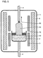
- Fig. 5 shows an example of such an apparatus using a stainless steel-made high pressure chamber.
- a cross sectional view of a schematic structure of an apparatus of producing a semiconductor crystal employed in the pulling method is shown.
- the apparatus includes a crucible 2 supported by a lower shaft 4, and a carbon heater 3 in a stainless steel high pressure chamber 11.
- a heat insulator 5 is provided between carbon heater 3 and stainless steel high pressure chamber 11 to prevent damage of chamber 11 caused by the heat of carbon heater 3.
- crucible 2 is first filled with GaAs material to prepare material melt 60 by the heat from carbon heater 3.
- the surface of material melt 60 is encapsulated by a liquid encapsulation material 70 in order to prevent evaporation of As from material melt 60.
- a pull shaft 14 having a seed crystal 55 attached at the leading end is pulled upward as indicated by the arrow to effect crystal growth under a high pressure atmosphere.
- a GaAs single crystal 50 is obtained.
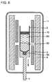
- Fig. 6 shows another example of an apparatus employing a stainless steel high pressure chamber.
- a cross sectional view of a schematic structure of an apparatus of producing a semiconductor crystal employed in the vertical boat method such as the VB or VGF method is shown.
- the apparatus has seed crystal 55 placed at the lower portion of crucible 2.
- material melt 60 is solidified from seed crystal 55 sequentially upwards for crystal growth.
- the remaining structure is similar to that of the apparatus of Fig. 5. Therefore, description thereof will not be repeated.
- an apparatus having a crucible or boat that stores material melt sealed in vacuum in a quartz ampoule, which is heated from the outer side.
- Such an apparatus is used in the horizontal boat method including the HB or HGF method, and in the vertical boat method including the VB or VGF method.
- Fig. 7 is a sectional view showing a schematic structure of such an apparatus employing a quartz ampoule.
- the apparatus has crucible 2 sealed within a quartz ampoule 21.
- a heater 3 such as of kanthal is provided outside ampoule 21.
- Quartz ampoule 21 is supported by lower shaft 4.
- a crystal is grown by moving lower shaft 4 downwards as indicated by the arrow or by shifting the temperature distribution.
- the As injection method of effecting reaction between the Ga in the crucible and the arsenic vapor generated by controlling the temperature of the As source outside the crucible, and the method of charging both the Ga and the As into the crucible together and raising the temperature for a direct reaction are known. Both methods are carried out in a high pressure chamber under liquid encapsulation. It is particularly noted that the latter requires high pressure of several ten atmospheres since the arsenic vapor pressure becomes considerably high.
- Production of a GaAs polycrystal is carried out by cooling the material obtained as described above.
- Production of a single crystal is carried out by the method of charging the prepared polycrystal into a crucible as the material, and the method of growing a single crystal subsequent to the raw material synthesization.
- carbon (or graphite) is employed for the heater material. Heating up to a temperature as high as approximately 1300°C is required in preparing the material melt since the melting point of GaAs is 1238°C.
- the vapor pressure of carbon is small even at the high temperature of approximately 1300°C. Therefore, carbon is suitable to be used for the heater.
- carbon is an element that is electrically active in a GaAs semiconductor single crystal. Therefore, the concentration of the carbon must be controlled in order to obtain a single crystal of high quality.
- various measures must be taken to control the electrical properties of GaAs crystal since the carbon and the synthesized GaAs reside in the same spacing. Thus, there is a problem that the furnace cost is increased.
- Japanese Patent Laying-Open No. 7-221038 discloses an example of using silicon carbide in the annealing furnace of a semiconductor. However, this publication is silent about the advantage of using such an apparatus in the growth of a single crystal.
- Japanese Patent Laying-Open No. 2-233578 discloses an apparatus of growing a semiconductor single crystal such as GaAs according to the pulling method with the entire apparatus placed in a stainless steel chamber.
- This apparatus is characterized in that a solid gasket is used as the heat-proof sealing material since the chamber made of silicon carbide is subjected to high temperature.
- the heat-proof sealing member has poor airtightness, so that sufficient difference between the inside pressure and the outside pressure cannot be achieved.
- Japanese Patent Laying-Open No. 2-120292 discloses an embodiment that employs silicon carbide for the crucible. However, this publication is completely silent about using silicon carbide for the reactor tube.
- an object of the present invention is to provide a semiconductor crystal such as GaAs that meets the requirement of high quality and large size, and a semiconductor crystal substrate using the same.
- Another object of the present invention is to provide a method and apparatus of producing such a semiconductor crystal at low cost.
- an apparatus of producing a semiconductor crystal includes a reactor tube having an open end in at least one end, formed of a material selected from the group consisting of silicon carbide, silicon nitride, aluminum nitride, and aluminum oxide, or of a composite material with any one of a material selected from the group consisting of silicon carbide, silicon nitride, aluminum nitride, boron nitride, aluminum oxide, magnesium oxide, mullite, and carbon as a base, and having an oxidation-proof or airtight film formed on the surface of the base; heat means arranged around the reactor tube, in the atmosphere; a flange attached at the open end to seal the reactor tube; and a crucible placed within the reactor tube to store the material of a semiconductor crystal.
- mullite refers to a mixture of aluminum oxide and silicon oxide.
- oxidation-proof or airtight film a thin film and the like such as of silicon carbide, silicon nitride, aluminum nitride, aluminum oxide, or silicon oxide can be enumerated. Such a film can be formed by a coat on a base.
- reactor tube of composite material a reactor tube having the above-described oxidation-proof or airtight film coat on the surface of a base formed of carbon such as graphite, or having the surface of the silicon carbide base oxidized can be used.
- a reactor tube having the oxidation-proof ability improved by forming a thin film of silicon oxide on the surface of the base by coating can be used.
- an apparatus of producing a semiconductor crystal includes a reactor tube having an open end in at least one end portion, formed of any one material selected from the group consisting of silicon carbide, silicon nitride, aluminum nitride, and aluminum oxide, or of a composite material with any one of a material selected from the group consisting of silicon carbide, silicon nitride, aluminum nitride, boron nitride, aluminum oxide, magnesium oxide, mullite, and carbon as the base, and having an oxidation-proof or airtight film formed on the surface of the base; heat means arranged around the reactor tube in the atmosphere; a flange attached at the open end to seal the reactor tube; a crucible placed within the reactor tube to store material of a semiconductor crystal; a seal member to seal the junction portion between the flange and the open end of the reactor tube; and seal maintain means to maintain the temperature of the junction portion between the flange and the open end of the reactor tube so that the sealing
- the semiconductor crystal also includes a silicon semiconductor, a germanium semiconductor, and the like, in addition to the compound semiconductor such as GaAs, CdTe, InAs, GaSb. Also, it is assumed that the semiconductor crystal includes a single crystal and a polycrystal.
- a heat insulator can be provided between the heating portion of the reactor tube by the heat means and the junction portion between the flange and the open end of the reactor tube.
- cooling water can be circulated within a jacket attached to the flange.
- the junction portion between the flange and the open end of the reactor tube can be air-cooled.
- the present invention preferably further includes a shaft member coupled to the crucible via the flange.
- the reactor tube is preferably arranged and used in the vertical direction.
- the shaft member is movable upwards and downwards in the crucible placed inside the reactor tube.
- the present invention preferably further includes at least one temperature measurement means in the proximity of the crucible via the flange.
- GaAs crystal can be cited as an example of the semiconductor crystal.
- pressure inside the reactor tube is preferably maintained to be higher than the atmospheric pressure, and the pressure outside the reactor tube is preferably the atmospheric pressure.
- the present invention preferably further includes a reservoir to store a second material of the semiconductor crystal in the reactor tube.
- the reservoir preferably includes a pipe to introduce gas of the second material into the crucible.
- the material accommodated within the crucible is Ga
- the second material accommodated in the reservoir is As
- a method of producing a semiconductor crystal includes the steps of placing a crucible in which the material of semiconductor crystal is stored in a reactor tube having an open end in at least one end portion, formed of any one material selected from the group consisting of silicon carbide, silicon nitride, aluminum nitride and aluminum oxide, or of a composite material with any one of a material selected from the group consisting of silicon carbide, silicon nitride, aluminum nitride, boron nitride, aluminum oxide, magnesium oxide, mullite, and carbon as a base, and having an oxidation-proof or airtight film formed on the surface of the base; attaching a flange at the open end to seal the reactor tube; maintaining the interior of the reactor tube under inert gas atmosphere; forming material melt by a heat means arranged around the reactor tube in the atmosphere; and growing a semiconductor crystal by solidifying the material melt.
- the semiconductor crystal is a GaAs crystal.
- the step of placing the crucible in which the material of a semiconductor crystal is stored in a reactor tube includes the steps of filling the crucible with Ga, filling a reservoir having a pipe with As, placing the crucible with the Ga and the reservoir with the As in the reactor tube.
- the step of forming material melt includes the steps of heating the Ga in the crucible up to a temperature higher than the melting point of GaAs by a heat means, heating and sublimating the As in the reservoir to generate arsenic vapor, and introducing the generated arsenic vapor to the Ga via the pipe to form GaAs melt in the crucible.
- the step of growing a semiconductor crystal in the present invention can be carried out using any crystal growth method selected from the group consisting of the VB method, VGF method, and pulling method.
- a semiconductor crystal is provided.
- This semiconductor crystal is formed of a compound, and has a diameter of at least 6 inches.
- the average dislocation density is not more than 1 ⁇ 10 4 cm -2 .
- a semiconductor crystal substrate is provided.
- This semiconductor crystal substrate is formed of a compound, and has a diameter of at least 6 inches.
- the average dislocation density is not more than 1 ⁇ 10 4 cm -2 .
- average dislocation density refers to the in-plane average value of the dislocation density for a substrate cut out from a crystal and that is etched and evaluated as the etch pit density.
- average dislocation density is not more than 1 ⁇ 10 4 cm -2 , implies that the average dislocation density is not more than 1 ⁇ 10 4 cm -2 even for a substrate of at least 6 inches in diameter cut out from any position of the crystal.
- the apparatus of producing a semiconductor crystal of the present invention is characterized in that a reactor tube is included formed of any one material selected from the group consisting of silicon carbide, silicon nitride, aluminum nitride, and aluminum oxide, or of a composite material with any one of a material selected from the group consisting of silicon carbide, silicon nitride, aluminum nitride, boron nitride, aluminum oxide, magnesium oxide, mullite, and carbon as the base, and having an oxidation-proof or airtight film formed on the surface of the base. Therefore, the possibility of deformation or breakage of the reactor tube such as in the case of using the conventional quartz ampoule is eliminated. A large amount of the material can be charged to produce a crystal of a large size.
- the usage of a reactor tube formed of silicon carbide is advantageous in that the cost is lower than that of the conventional stainless steel high pressure chamber. Therefore, the furnace cost in producing a semiconductor crystal according to the present invention can be lowered considerably.
- a reactor tube formed of silicon nitride, formed of aluminum nitride, formed of aluminum oxide, or formed of a base that does not include carbon such as silicon nitride, aluminum nitride, boron nitride, aluminum oxide, magnesium oxide, mullite, and the like is used, introduction of carbon into the semiconductor material can be prevented. As a result, a semiconductor material of high purity can be achieved.
- the reactor tube has an open end in at least one end portion. A flange is attached at this open end. Therefore, the reactor tube can be used repeatedly, opposed to the case where the conventional quartz ampoule is used. Accordingly, the production cost can be reduced.
- the material can be synthesized in situ.
- Application to the As injection method is allowed.
- the partial pressure of the atmospheric gas within the chamber can be controlled in situ to facilitate adjustment of the impurity concentration.
- a semiconductor single crystal where the deviation of the carbon concentration in the direction of the length is extremely small can be obtained.
- the semiconductor crystal of the present invention has a diameter of at least 6 inches.
- the average dislocation density is not more than 1 ⁇ 10 4 cm -2 .
- the defect density is extremely low.
- the practical method of producing GaAs is mainly classified into the pulling method (LEC method) and the boat method (VB method) as mentioned before.
- the method of the present invention can be employed in both methods. Specifically, an example of the VB method is shown in the first embodiment, and an example of the LEC method is shown in the third embodiment.
- the present invention is applicable, not only in the production of a semiconductor single crystal, but also in the synthesization of a semiconductor material such as a GaAs polycrystal that becomes the material thereof.
- a pulverized version of the GaAs polycrystal compact obtained in the second embodiment can be used as the material in the first or third embodiment.
- seed crystal is used. However, in the second embodiment, seed crystal is not used.
- the advantage of the present invention is most appreciable when a semiconductor single crystal is grown by the VB method.
- a semiconductor crystal at least 6 inches in diameter with the average dislocation density of not more than 1 ⁇ 10 4 cm -2 can easily be obtained.
- a semiconductor crystal having an average dislocation density of approximately 1 to 5 ⁇ 10 3 cm -2 can be grown.
- the electrical property can be made uniform by such a low dislocation density.
- a semiconductor crystal with the concentration of boron (B) less than 3 ⁇ 10 16 cm -3 , preferably not more than 1 ⁇ 10 16 cm -3 can be grown. It is said that boron (B) reduces the activation factor after ion implantation. Therefore, the device performance can be improved by reducing the concentration of boron (B).
- the semiconductor crystal of the present invention has a low residual strain since the occurrence of dislocation is low. Therefore, the strength sufficient for practical usage can be achieved with the thickness of 500-700 ⁇ m even when the size becomes greater.
- the average residual strain of the substrate measured using the photoelastic effect is not more than 1 ⁇ 10 -5 .
- the semiconductor crystal of the present invention as an ingot is characterized in that the deviation of the carbon concentration in the direction of the length is extremely small.
- the carbon (C) concentration distribution can be made uniform along the direction of the length by controlling the concentration of the CO gas in the reactor tube.
- a compound semiconductor single crystal ingot can be obtained that has a diameter of at least 6 inches, the average dislocation density of less than 1 ⁇ 10 4 cm -2 , and having the carbon concentration restricted to be within ⁇ 50% with respect to the target value over the region of 0.1-0.8 in fraction solidified.
- the carbon concentration of the actually obtained crystal has variation of the carbon concentration restricted within ⁇ 50% with respect to the set value over the entire length. Therefore, there is the advantage that the yield is improved when the substrate is cut out from this ingot.
- variation in the carbon concentration can be reduced by the present invention is due to the critical controllability of the concentration of the CO gas in the reactor tube during the growth. This advantage becomes more effective by selecting a material that does not include carbon for the reactor tube or by coating the reactor tube with a material that does not include carbon.
- a carbon heater is not used in the present invention in contrast to the case of crystal growth by the conventional high pressure chamber. This means that a crystal can be grown with the interior of the reactor tube under a carbon-free condition. Therefore, the distribution of the carbon concentration can be made uniform.
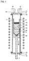
- Fig. 1 is a sectional view of the schematic structure of an apparatus of producing a semiconductor crystal according to a first embodiment of the present invention.
- the apparatus includes a silicon carbide reactor tube 1 and a kanthal heater 3.
- Silicon carbide reactor tube 1 has an inner diameter of 170 mm and a thickness of 3 mm with an open end at both end sides.
- Kanthal heater 3 is arranged around reactor tube 1 in the atmosphere with 5 zones.
- the first embodiment is characterized in that the heater is not externally shielded, as shown in Fig. 1.
- a carbon heater of low reactivity was used to grow a crystal within a high pressure chamber.
- the first embodiment of the present invention has a heater provided in the atmosphere outside the reactor tube. Therefore, a heater based on iron and the like that is low in cost can be used. This type of heater can easily provide multi zones. Therefore, favorable controllability of a temperature distribution can be provided.
- a carbon heater is not used, a crystal can be grown with the interior of the silicon carbide reactor tube under a carbon-free state. Therefore, variation in the carbon concentration in the crystal can be reduced.
- a stainless steel flange 9 is attached at both at the open ends of silicon carbide reactor tube 1.
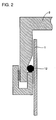
- Fig. 2 is a partial enlarged sectional view of the junction between silicon carbide reactor tube 1 and stainless steel flange 9.
- the junction portion of silicon carbide reactor tube 1 and stainless steel flange 9 has the Wilson seal structure with a packing 12 therebetween to ensure the airtightness.
- An elastic member such as an O-ring is used as packing 12. More specifically, fluorine-contained polymers and the like can be used as well as rubber.
- the range of selectivity for the material that can be used as packing 12 is wide. This is because there is no possibility of the material of packing 12 that is located outside silicon carbide reactor tube 1 being incorporated as an impurity into the semiconductor crystal that is grown in reactor tube 1.
- the seal portion of the junction between silicon carbide reactor tube 1 and stainless steel flange 9 is provided at the low temperature part.
- rubber or a material of fluorine-contained polymers and the like that is superior in airtightness can be used as the sealing material. Therefore, sufficient difference between the inside and outside pressure of silicon carbide reactor tube 1 can be achieved.
- a jacket is attached to flange 9.
- the junction portion between silicon carbide reactor tube 1 and flange 9 is cooled by circulating cooling water within the jacket. Thus, the airtightness can be maintained even during heating by heater 3.
- Airtightness at the junction between silicon carbide reactor tube 1 and flange 9 can be maintained by means other than the jacket.
- the junction portion can be forcefully air cooled, or the reactor tube separated sufficiently apart from the junction portion to be cooled by the atmosphere.
- a port 16 for inserting an exhaust tube and a port 17 for inserting a gas inlet tube are provided in flange 9 attached at the upper portion of silicon carbide reactor tube 1.
- An exhaust tube 18 is inserted into port 16 to exhaust the interior of silicon carbide reactor tube 1 for vacuum.
- a gas inlet tube 19 is inserted in port 17 to introduce gas into silicon carbide reactor tube 1.
- a lower shaft 4 that is movable upwards and downwards pierces the center of flange 9 that is attached at the lower portion of silicon carbide reactor tube 1.
- a crucible 2 to accommodate the material of the crystal is mounted at the leading end of lower shaft 4.
- thermocouple port 15 is formed at flange 9 attached to the lower portion of silicon carbide reactor tube 1.
- a thermocouple 13 to measure the temperature in the proximity of the side of crucible 2 is inserted into port 15.
- a thermocouple port can be formed at the upper flange to insert a thermocouple into the crucible from above.
- a thermocouple can be provided inside the lower shaft to measure the temperature at the bottom of the crucible.
- a radiation thermometer can be used as the temperature measurement means in addition to the thermocouple.
- a GaAs single crystal with 6 inches in diameter is produced by the VB method as set forth in the following.
- a seed crystal of a GaAs single crystal is placed at the cap portion at the lower end of crucible 2 with 6 inches in diameter mounted at the leading end of lower shaft 4. Then, 20 kg of GaAs polycrystalline material and 300g of B 2 O 3 70 to encapsulate the surface of material melt 60 are charged into crucible 2.
- This crucible is installed within silicon carbide reactor tube 1.
- Flange 9 is attached for sealing.
- silicon carbide reactor tube 1 is evacuated through exhaust pipe 18.
- the temperature is raised by kanthal heater 3.
- nitrogen gas is introduced into silicon carbide reactor tube 1 through gas inlet tube 19.
- the pressure in silicon carbide reactor tube 1 is adjusted to approximately 2 atmospheres when the temperature is completely raised.
- the GaAs polycrystalline material is melted by the heat of kanthal heater 3 to produce material melt 60.
- the temperature of the seed crystal is adjusted to be in the vicinity of 1238°C that is the melting point of GaAs.
- the temperature at the side surface of crucible 2 is adjusted to be approximately 1250°C. Then, lower shaft 4 is moved downwards as indicated by the arrow at the speed of 2 mm/h.
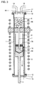
- Fig. 3 is a sectional view showing a schematic structure of an apparatus of producing a semiconductor crystal according to a second embodiment of the present invention.
- the reactor tube of the second embodiment is formed of aluminum nitride.
- the apparatus has kanthal heater 3 of five zones divided into the upper one zone and the lower four zones by the interposition of a heat insulator 8.
- Heat insulator 8 is provided also inside aluminum nitride reactor tube 1 corresponding to the height of heat insulator 8 provided between the heater.
- Crucible 2 is placed within aluminum nitride reactor tube 1 at the position lower than heat insulator 8.
- a reservoir 6 is placed in aluminum nitride reactor tube 1 at a position upper than heat insulator 8.
- a pipe 7 is connected to reservoir 6. Pipe 7 is formed so that the leading end is located in material melt 60 that is charged into crucible 2.
- a GaAs polycrystal of 6 inches in diameter is produced by the VB method as set forth in the following.
- aluminum nitride reactor tube 1 is evacuated through exhaust tube 18.
- the temperature is raised by kanthal heater 3.
- the temperature of thermocouple 14 placed at the side of crucible 2 is adjusted to be approximately 1250°C.
- the temperature in reservoir 6 is adjusted to be kept below 500°C.
- nitrogen gas is introduced into aluminum nitride reactor tube 1 through gas inlet tube 19.
- the pressure in aluminum nitride reactor tube 1 is adjusted to be approximately 2 atmospheres at the completion of the temperature rise.
- the temperature at the bottom of crucible 2 is adjusted to be in the vicinity of 1238°C which is the melting point of GaAs, subsequent to the completion of the reaction for the formation of the GaAs melt. Then, lower shaft 4 is moved downwards as indicated by the arrow at the speed of 10 mm/h.
- GaAs polycrystal 50 is grown.
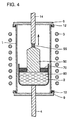
- Fig. 4 is a sectional view showing a schematic structure of an apparatus of producing a semiconductor crystal according to a third embodiment of the present invention.
- the reactor tube of the present embodiment is formed of aluminum oxide.
- the apparatus of Fig. 4 is mainly used in the pulling method.
- the apparatus includes an aluminum oxide reactor tube 1 having an open end at both end sides, and a heater 3 arranged around aluminum oxide reactor tube 1.
- a flange 9 is attached at both the open ends of aluminum oxide reactor tube 1.
- Lower shaft 4 pierces the center of the flange 9 attached at the lower end of aluminum oxide reactor tube 1.
- Crucible 2 is mounted at the leading end of lower shaft 4.
- a pull shaft 14 that is movable upwards and downwards pierces the center of flange 9 attached at the upper portion of aluminum oxide reactor tube 1.
- a crystal is grown by drawing up pull shaft 4 in the direction of the arrow.
- the apparatus of the present embodiment includes an aluminum oxide reactor tube that has both ends open.
- the open end of the aluminum oxide reactor tube is required to be formed at only at least one end side for all the methods other than the pulling method.
- a method and apparatus for production used in the VB method or the pulling method are shown in the above embodiments.
- the present invention is also applicable to the production of a semiconductor crystal by the vertical boat method such as the VGF method or the horizontal boat method such as the HB method and the HGF method.
- the present invention is also applicable to produce a compound semiconductor crystal such as CdTe crystal, InAs crystal, GaSb crystal, silicon semiconductor crystal, and germanium semiconductor crystal.
- an aluminum oxide reactor tube is used.
- a reactor tube formed of elementary substance of silicon nitride, aluminum nitride, or silicon carbide can be used in addition to the elementary substance of aluminum oxide.
- the reactor tube can be formed of a composite material with silicon carbide, silicon nitride, aluminum nitride, boron nitride, aluminum oxide, magnesium oxide, mullite, and carbon as the base and having an oxidation-proof or airtight film formed on the surface thereof.
- a GaAs crystal of 6 inches in diameter was actually produced by the VB method using a silicon carbide reactor tube as shown in the first embodiment. As a result, a single crystal with 25 cm in length was obtained. The obtained crystal had a low dislocation density. Variation in the carbon concentration was small by virtue of the concentration of the CO gas in the reactor tube being controlled during the growth. Thus, a crystal of high quality was obtained.
- the average yield was 50% when a similar crystal growth was carried out six times. Taking into consideration the difference in cost between the conventional apparatus including a stainless steel high pressure chamber and an apparatus including the silicon carbide reactor tube of the present example, it was found that the cost of producing a GaAs single crystal can be lowered by approximately 20% than the case where a stainless steel high pressure vessel is used.
- GaAs crystal of 6 inches in diameter was actually produced using an aluminum nitride reactor tube as shown in the second embodiment.
- GaAs polycrystal of approximately 30 kg was obtained.
- the purity of the obtained polycrystal was analyzed. Only the matrix element, carbon and boron were detected. The other elements were below the detection limit. The quality of the crystal was extremely high.
- a GaAs crystal of 6 inches in diameter was actually produced by the LEC method using an aluminum oxide reactor tube, as shown in the third embodiment.
- the temperature gradient must be increased in the LEC method to prevent the evaporation of As during crystal growth. Therefore, the values of the average dislocation density and the residual strain of the obtained crystal were higher than those of the crystal obtained in Example 1.
- controllability of the temperature distribution was superior since the number of zones in the heater could be easily increased in the present example. As a result, generation of polycrystal at the latter stage of the crystal growth could be prevented. A single crystal could be grown that is longer than that of Comparative Example 1 that will be described subsequently.
- a GaAs crystal of 6 inches in diameter was produced by the conventional LEC method shown in Fig. 5.
- Example 3 The temperature gradient had to be increased as in Example 3 to prevent the evaporation of As during the crystal growth. Therefore, the values of the average dislocation density and the residual strain of the obtained crystal were greater than those of the crystal obtained in Example 1.
- the controllability of the temperature distribution is limited since the number of zones in the heater cannot be increased too much due to the structure in the conventional LEC method. Therefore, generation of polycrystal could not be prevented at the latter stage of the crystal growth.
- the length of the single crystal was shorter than that of Example 3.
- a GaAs crystal of 6 inches in diameter was produced by the conventional liquid encapsulated VB method shown in Fig. 6.
- a GaAs crystal of 4 inches in diameter was grown by the conventional quartz ampoule sealed VB method shown in Fig. 7.
- the carbon concentration in the quartz ampoule during crystal growth could not be controlled.
- the uniformity of the carbon concentration was poor.
- Si doped GaAs was grown by the VGF method under the pressure of 2 atm of N 2 gas using an airtight reactor tube of silicon carbide of high purity. As a result, a single crystal with 20 cm in length and 3 inches in diameter was obtained.
- the purity of the obtained crystal was analyzed. It is found that over the entire crystal, the concentration of all the impurities including carbon was not more than 5 ⁇ 10 14 cm -3 except for Si. The obtained crystal was extremely high in purity.
- Undoped GaAs was grown by the VGF method under the N 2 gas pressure of 1.2 atm using a reactor tube of a composite material having the surface of a base of graphite coated with silicon carbide to a thickness of 50 ⁇ m. It was confirmed that the reactor tube had the sufficient airtightness with the arrived degree of vacuum of not more than 1 ⁇ 10 -2 Torr. As a result, a single crystal of 30 cm in length and 3 inches in diameter was obtained.
- the purity of the obtained crystal was analyzed: It was found that, over the entire crystal, the carbon concentration was 1 ⁇ 2 ⁇ 10 15 cm -3 , and the concentration of the other impurities was not more than 5 X 10 14 cm -3 .
- the resistivity was 1 ⁇ 3 ⁇ 10 7 ⁇ cm. Thus, a GaAs crystal of extremely favorable semi-insulating property was obtained.
- a Si doped GaAs was grown by the VGF method under the Ar gas pressure of 1.5 atm using a reactor tube formed of a composite material having the surface of a base of porous mullite of low purity coated with aluminum oxide of high purity to a thickness of 100 ⁇ m. It was confirmed that the reactor tube had sufficient airtightness with the arrived degree of vacuum of not more than 1 ⁇ 10 -3 Torr. As a result, a single crystal of 3 inches in diameter and 15 cm in length was obtained.
- the purity of the obtained crystal was analyzed.
- the concentration of all the impurities including carbon was not more than 5 ⁇ 10 14 cm -3 except for Si over the entire crystal. Thus, the purity was extremely high.
Abstract
Description
- The present invention relates to a semiconductor crystal, and a method and apparatus of producing the same. Particularly, the present invention relates to a semiconductor crystal for use in production of a GaAs substrate and the like employed in an optical device, an electronic device, and the like, and a method and apparatus of producing such a semiconductor crystal.
- A GaAs crystal, for example, among the semiconductor crystals, is produced industrially by the pulling method (LEC method), the horizontal boat method (HB method, HGF method), and the vertical boat method (VB method, VGF method). The pulling method and the vertical boat method are particularly advantageous over the horizontal boat method for producing a single crystal since the yield is improved due to the cross section of the obtained crystal being circular identical to that of the substrate and since the diameter can easily be increased due to the symmetry of the thermal environment in the growth system.
- As an example of an apparatus of producing a semiconductor crystal, an apparatus having a carbon heater and a crucible that stores material melt placed in a stainless steel-made high pressure chamber is known. Such an apparatus is used in the LEC, the VB, or the VGF method.
- Fig. 5 shows an example of such an apparatus using a stainless steel-made high pressure chamber. A cross sectional view of a schematic structure of an apparatus of producing a semiconductor crystal employed in the pulling method is shown.
- Referring to Fig. 5, the apparatus includes a
crucible 2 supported by alower shaft 4, and acarbon heater 3 in a stainless steelhigh pressure chamber 11. Aheat insulator 5 is provided betweencarbon heater 3 and stainless steelhigh pressure chamber 11 to prevent damage ofchamber 11 caused by the heat ofcarbon heater 3. - In growing a crystal using such an apparatus,
crucible 2 is first filled with GaAs material to preparematerial melt 60 by the heat fromcarbon heater 3. The surface ofmaterial melt 60 is encapsulated by aliquid encapsulation material 70 in order to prevent evaporation of As frommaterial melt 60. Apull shaft 14 having aseed crystal 55 attached at the leading end is pulled upward as indicated by the arrow to effect crystal growth under a high pressure atmosphere. Thus, a GaAssingle crystal 50 is obtained. - Fig. 6 shows another example of an apparatus employing a stainless steel high pressure chamber. A cross sectional view of a schematic structure of an apparatus of producing a semiconductor crystal employed in the vertical boat method such as the VB or VGF method is shown.
- Referring to Fig. 6, the apparatus has
seed crystal 55 placed at the lower portion ofcrucible 2. By movinglower shaft 4 downwards as indicated by the arrow or by shifting the temperature distribution,material melt 60 is solidified fromseed crystal 55 sequentially upwards for crystal growth. The remaining structure is similar to that of the apparatus of Fig. 5. Therefore, description thereof will not be repeated. - As another example of an apparatus for crystal growth, an apparatus is known having a crucible or boat that stores material melt sealed in vacuum in a quartz ampoule, which is heated from the outer side. Such an apparatus is used in the horizontal boat method including the HB or HGF method, and in the vertical boat method including the VB or VGF method.
- Fig. 7 is a sectional view showing a schematic structure of such an apparatus employing a quartz ampoule.
- Referring to Fig. 7, the apparatus has
crucible 2 sealed within aquartz ampoule 21. Aheater 3 such as of kanthal is provided outsideampoule 21.Quartz ampoule 21 is supported bylower shaft 4. A crystal is grown by movinglower shaft 4 downwards as indicated by the arrow or by shifting the temperature distribution. - As a method of synthesizing the GaAs material for crystal growth, the As injection method of effecting reaction between the Ga in the crucible and the arsenic vapor generated by controlling the temperature of the As source outside the crucible, and the method of charging both the Ga and the As into the crucible together and raising the temperature for a direct reaction are known. Both methods are carried out in a high pressure chamber under liquid encapsulation. It is particularly noted that the latter requires high pressure of several ten atmospheres since the arsenic vapor pressure becomes considerably high.
- Production of a GaAs polycrystal is carried out by cooling the material obtained as described above. Production of a single crystal is carried out by the method of charging the prepared polycrystal into a crucible as the material, and the method of growing a single crystal subsequent to the raw material synthesization.
- There is the demand for a larger semiconductor crystal as the integration density of a semiconductor device becomes higher. Currently, a GaAs crystal with 4 inches in diameter is of practical usage as for a compound semiconductor crystal. The need of increasing the size of such a compound semiconductor crystal has become greater to induce various research and development. However, there are many problems on the mass production of a large compound semiconductor crystal. Production of a large compound semiconductor crystal greater than 4 inches is not yet practical.
- For example, when the stainless steel high pressure chamber shown in Fig. 5 or 6 is used, a heat insulating layer must be inserted between the heater and the stainless steel chamber. Accordingly, the size of the furnace becomes larger to increase the furnace cost.
- According to the method shown in Fig. 5 or 6, carbon (or graphite) is employed for the heater material. Heating up to a temperature as high as approximately 1300°C is required in preparing the material melt since the melting point of GaAs is 1238°C. Here, the vapor pressure of carbon is small even at the high temperature of approximately 1300°C. Therefore, carbon is suitable to be used for the heater. However, carbon is an element that is electrically active in a GaAs semiconductor single crystal. Therefore, the concentration of the carbon must be controlled in order to obtain a single crystal of high quality. When the method employing the stainless steel high pressure chamber shown in Fig. 5 or 6 is to be carried out, various measures must be taken to control the electrical properties of GaAs crystal since the carbon and the synthesized GaAs reside in the same spacing. Thus, there is a problem that the furnace cost is increased.
- In the case where the quartz ampoule shown in Fig. 7 is used, there was a problem that it is difficult to produce a large crystal by charging a great amount of the material since there is a possibility of deformation or breakage of the ampoule. There is also a problem that the material cannot be synthesized, in situ, since the ampoule is sealed, barring the application of the As injection method. There is also the problem that the atmospheric gas cannot be controlled after the ampoule is sealed.
- Japanese Patent Laying-Open No. 7-221038 discloses an example of using silicon carbide in the annealing furnace of a semiconductor. However, this publication is silent about the advantage of using such an apparatus in the growth of a single crystal.
- Japanese Patent Laying-Open No. 2-233578 discloses an apparatus of growing a semiconductor single crystal such as GaAs according to the pulling method with the entire apparatus placed in a stainless steel chamber. This apparatus is characterized in that a solid gasket is used as the heat-proof sealing material since the chamber made of silicon carbide is subjected to high temperature. However, the heat-proof sealing member has poor airtightness, so that sufficient difference between the inside pressure and the outside pressure cannot be achieved.
- Japanese Patent Laying-Open No. 2-120292 discloses an embodiment that employs silicon carbide for the crucible. However, this publication is completely silent about using silicon carbide for the reactor tube.
- Thus, the need of a large GaAs semiconductor single crystal with at least 6 inches in diameter has become greater in response to the semiconductor device scaled to higher integration density. A semiconductor crystal of a high quality is required at low cost.
- In view of the foregoing, an object of the present invention is to provide a semiconductor crystal such as GaAs that meets the requirement of high quality and large size, and a semiconductor crystal substrate using the same.
- Another object of the present invention is to provide a method and apparatus of producing such a semiconductor crystal at low cost.
- According to an aspect of the present invention, an apparatus of producing a semiconductor crystal is provided. The apparatus includes a reactor tube having an open end in at least one end, formed of a material selected from the group consisting of silicon carbide, silicon nitride, aluminum nitride, and aluminum oxide, or of a composite material with any one of a material selected from the group consisting of silicon carbide, silicon nitride, aluminum nitride, boron nitride, aluminum oxide, magnesium oxide, mullite, and carbon as a base, and having an oxidation-proof or airtight film formed on the surface of the base; heat means arranged around the reactor tube, in the atmosphere; a flange attached at the open end to seal the reactor tube; and a crucible placed within the reactor tube to store the material of a semiconductor crystal.
- In the present specification, "mullite" refers to a mixture of aluminum oxide and silicon oxide.
- As "oxidation-proof or airtight film", a thin film and the like such as of silicon carbide, silicon nitride, aluminum nitride, aluminum oxide, or silicon oxide can be enumerated. Such a film can be formed by a coat on a base.
- As " reactor tube of composite material", a reactor tube having the above-described oxidation-proof or airtight film coat on the surface of a base formed of carbon such as graphite, or having the surface of the silicon carbide base oxidized can be used. Alternatively, a reactor tube having the oxidation-proof ability improved by forming a thin film of silicon oxide on the surface of the base by coating can be used.
- According to another aspect of the present invention, an apparatus of producing a semiconductor crystal is provided. The apparatus includes a reactor tube having an open end in at least one end portion, formed of any one material selected from the group consisting of silicon carbide, silicon nitride, aluminum nitride, and aluminum oxide, or of a composite material with any one of a material selected from the group consisting of silicon carbide, silicon nitride, aluminum nitride, boron nitride, aluminum oxide, magnesium oxide, mullite, and carbon as the base, and having an oxidation-proof or airtight film formed on the surface of the base; heat means arranged around the reactor tube in the atmosphere; a flange attached at the open end to seal the reactor tube; a crucible placed within the reactor tube to store material of a semiconductor crystal; a seal member to seal the junction portion between the flange and the open end of the reactor tube; and seal maintain means to maintain the temperature of the junction portion between the flange and the open end of the reactor tube so that the sealing function can be maintained by the sealing member.
- In the invention of the present application, the semiconductor crystal also includes a silicon semiconductor, a germanium semiconductor, and the like, in addition to the compound semiconductor such as GaAs, CdTe, InAs, GaSb. Also, it is assumed that the semiconductor crystal includes a single crystal and a polycrystal.
- As an example of the seal maintain means, a heat insulator can be provided between the heating portion of the reactor tube by the heat means and the junction portion between the flange and the open end of the reactor tube.
- As another example of the seal maintain means, cooling water can be circulated within a jacket attached to the flange.
- As a further example of the seal maintain means, the junction portion between the flange and the open end of the reactor tube can be air-cooled.
- The present invention preferably further includes a shaft member coupled to the crucible via the flange.
- In the present invention, the reactor tube is preferably arranged and used in the vertical direction. The shaft member is movable upwards and downwards in the crucible placed inside the reactor tube.
- The present invention preferably further includes at least one temperature measurement means in the proximity of the crucible via the flange.
- In the present invention, GaAs crystal can be cited as an example of the semiconductor crystal.
- In the present invention, pressure inside the reactor tube is preferably maintained to be higher than the atmospheric pressure, and the pressure outside the reactor tube is preferably the atmospheric pressure.
- The present invention preferably further includes a reservoir to store a second material of the semiconductor crystal in the reactor tube. The reservoir preferably includes a pipe to introduce gas of the second material into the crucible.
- Further preferably, the material accommodated within the crucible is Ga, and the second material accommodated in the reservoir is As.
- According to a further aspect of the present invention, a method of producing a semiconductor crystal is provided. The method includes the steps of placing a crucible in which the material of semiconductor crystal is stored in a reactor tube having an open end in at least one end portion, formed of any one material selected from the group consisting of silicon carbide, silicon nitride, aluminum nitride and aluminum oxide, or of a composite material with any one of a material selected from the group consisting of silicon carbide, silicon nitride, aluminum nitride, boron nitride, aluminum oxide, magnesium oxide, mullite, and carbon as a base, and having an oxidation-proof or airtight film formed on the surface of the base; attaching a flange at the open end to seal the reactor tube; maintaining the interior of the reactor tube under inert gas atmosphere; forming material melt by a heat means arranged around the reactor tube in the atmosphere; and growing a semiconductor crystal by solidifying the material melt.
- In the present invention, the semiconductor crystal is a GaAs crystal. The step of placing the crucible in which the material of a semiconductor crystal is stored in a reactor tube includes the steps of filling the crucible with Ga, filling a reservoir having a pipe with As, placing the crucible with the Ga and the reservoir with the As in the reactor tube. The step of forming material melt includes the steps of heating the Ga in the crucible up to a temperature higher than the melting point of GaAs by a heat means, heating and sublimating the As in the reservoir to generate arsenic vapor, and introducing the generated arsenic vapor to the Ga via the pipe to form GaAs melt in the crucible.
- The step of growing a semiconductor crystal in the present invention can be carried out using any crystal growth method selected from the group consisting of the VB method, VGF method, and pulling method.
- According to still another aspect of the present invention, a semiconductor crystal is provided. This semiconductor crystal is formed of a compound, and has a diameter of at least 6 inches. The average dislocation density is not more than 1 × 104cm-2.
- According to a still further aspect of the present invention, a semiconductor crystal substrate is provided. This semiconductor crystal substrate is formed of a compound, and has a diameter of at least 6 inches. The average dislocation density is not more than 1 × 104cm-2.
- In the present specification, "average dislocation density" refers to the in-plane average value of the dislocation density for a substrate cut out from a crystal and that is etched and evaluated as the etch pit density.
- In the present invention, "average dislocation density is not more than 1 × 104cm-2,, implies that the average dislocation density is not more than 1 × 104cm-2 even for a substrate of at least 6 inches in diameter cut out from any position of the crystal.
- The apparatus of producing a semiconductor crystal of the present invention is characterized in that a reactor tube is included formed of any one material selected from the group consisting of silicon carbide, silicon nitride, aluminum nitride, and aluminum oxide, or of a composite material with any one of a material selected from the group consisting of silicon carbide, silicon nitride, aluminum nitride, boron nitride, aluminum oxide, magnesium oxide, mullite, and carbon as the base, and having an oxidation-proof or airtight film formed on the surface of the base. Therefore, the possibility of deformation or breakage of the reactor tube such as in the case of using the conventional quartz ampoule is eliminated. A large amount of the material can be charged to produce a crystal of a large size.
- The usage of a reactor tube formed of silicon carbide is advantageous in that the cost is lower than that of the conventional stainless steel high pressure chamber. Therefore, the furnace cost in producing a semiconductor crystal according to the present invention can be lowered considerably.
- When a reactor tube formed of silicon nitride, formed of aluminum nitride, formed of aluminum oxide, or formed of a base that does not include carbon such as silicon nitride, aluminum nitride, boron nitride, aluminum oxide, magnesium oxide, mullite, and the like is used, introduction of carbon into the semiconductor material can be prevented. As a result, a semiconductor material of high purity can be achieved.
- Even in the case where a base is used of a carbon material such as graphite that is not oxidation-proof, or a porous aluminum oxide or mullite that is not airtight, damage or fracture of the reactor tube can be prevented effectively by coating the surface of the base with oxidation-proof or airtight material. Since the material corresponding to such a base is extremely economical, a semiconductor crystal can be obtained at low cost according to the present invention.
- Even in the case where a base including carbon such as nitride carbide or graphite is used, introduction of carbon into the semiconductor material can be prevented by coating the surface with a material that does not include carbon. In the case where a base of low purity such as mullite is used, a semiconductor crystal of high purity can be achieved by coating the surface with a material of high purity.
- According to the present invention, the reactor tube has an open end in at least one end portion. A flange is attached at this open end. Therefore, the reactor tube can be used repeatedly, opposed to the case where the conventional quartz ampoule is used. Accordingly, the production cost can be reduced.
- Since a temperature measurement means is also provided in the proximity of the crucible, crystal growth of high reproducibility can be carried out.
- In contrast to the case where the ampoule is sealed, the material can be synthesized in situ. Application to the As injection method is allowed. Also, the partial pressure of the atmospheric gas within the chamber can be controlled in situ to facilitate adjustment of the impurity concentration.
- According to the present invention, a semiconductor single crystal where the deviation of the carbon concentration in the direction of the length is extremely small can be obtained.
- The semiconductor crystal of the present invention has a diameter of at least 6 inches. The average dislocation density is not more than 1 × 104cm-2. The defect density is extremely low.
- The foregoing and other objects, features, aspects and advantages of the present invention will become more apparent from the following detailed description of the present invention when taken in conjunction with the accompanying drawings.
-
- Fig. 1 is a sectional view showing a schematic structure of an apparatus of producing a semiconductor crystal according to a first embodiment of the present invention.
- Fig. 2 is a partial sectional view showing in enlargement the junction portion between the reactor tube and the stainless steel Range of Fig. 1.
- Fig. 3 is a sectional view showing a schematic structure of an apparatus of producing a semiconductor crystal according to a second embodiment of the present invention.
- Fig. 4 is a sectional view showing a schematic structure of an apparatus of producing a semiconductor crystal according to a third embodiment of the present invention.
- Figs. 5 and 6 are sectional views showing a schematic structure of examples of an apparatus of producing a semiconductor crystal using a conventional stainless steel high pressure vessel.
- Fig. 7 is a sectional view showing a schematic structure of an example of an apparatus producing a semiconductor crystal using a conventional quartz ampoule.
-
- The practical method of producing GaAs is mainly classified into the pulling method (LEC method) and the boat method (VB method) as mentioned before. The method of the present invention can be employed in both methods. Specifically, an example of the VB method is shown in the first embodiment, and an example of the LEC method is shown in the third embodiment. It is to be noted that the present invention is applicable, not only in the production of a semiconductor single crystal, but also in the synthesization of a semiconductor material such as a GaAs polycrystal that becomes the material thereof. For example, a pulverized version of the GaAs polycrystal compact obtained in the second embodiment can be used as the material in the first or third embodiment. In the first and third embodiments, seed crystal is used. However, in the second embodiment, seed crystal is not used.
- The advantage of the present invention is most appreciable when a semiconductor single crystal is grown by the VB method. According to the present invention, a semiconductor crystal at least 6 inches in diameter with the average dislocation density of not more than 1 × 104cm-2 can easily be obtained. By controlling the cooling method and the like, a semiconductor crystal having an average dislocation density of approximately 1 to 5 × 103cm-2 can be grown. The electrical property can be made uniform by such a low dislocation density.
- Furthermore, according to the present invention, a semiconductor crystal with the concentration of boron (B) less than 3 × 1016cm-3, preferably not more than 1 × 1016cm-3 can be grown. It is said that boron (B) reduces the activation factor after ion implantation. Therefore, the device performance can be improved by reducing the concentration of boron (B).
- The semiconductor crystal of the present invention has a low residual strain since the occurrence of dislocation is low. Therefore, the strength sufficient for practical usage can be achieved with the thickness of 500-700 µm even when the size becomes greater. The average residual strain of the substrate measured using the photoelastic effect is not more than 1 × 10⁻⁵.
- The semiconductor crystal of the present invention as an ingot is characterized in that the deviation of the carbon concentration in the direction of the length is extremely small. In other words, the carbon (C) concentration distribution can be made uniform along the direction of the length by controlling the concentration of the CO gas in the reactor tube. According to the present invention, a compound semiconductor single crystal ingot can be obtained that has a diameter of at least 6 inches, the average dislocation density of less than 1 × 104cm-2, and having the carbon concentration restricted to be within ± 50% with respect to the target value over the region of 0.1-0.8 in fraction solidified. In other words, when the carbon concentration is set to 1 × 1015cm-3, for example, the carbon concentration of the actually obtained crystal has variation of the carbon concentration restricted within ± 50% with respect to the set value over the entire length. Therefore, there is the advantage that the yield is improved when the substrate is cut out from this ingot. The reason why variation in the carbon concentration can be reduced by the present invention is due to the critical controllability of the concentration of the CO gas in the reactor tube during the growth. This advantage becomes more effective by selecting a material that does not include carbon for the reactor tube or by coating the reactor tube with a material that does not include carbon. Furthermore, a carbon heater is not used in the present invention in contrast to the case of crystal growth by the conventional high pressure chamber. This means that a crystal can be grown with the interior of the reactor tube under a carbon-free condition. Therefore, the distribution of the carbon concentration can be made uniform.
- An example of producing a semiconductor crystal of 6 inches in diameter will be described hereinafter. However, the present invention is applicable to production of a semiconductor crystal of a larger size such as 8 inches.
- Fig. 1 is a sectional view of the schematic structure of an apparatus of producing a semiconductor crystal according to a first embodiment of the present invention.
- Referring to Fig. 1, the apparatus includes a silicon
carbide reactor tube 1 and akanthal heater 3. Siliconcarbide reactor tube 1 has an inner diameter of 170 mm and a thickness of 3 mm with an open end at both end sides.Kanthal heater 3 is arranged aroundreactor tube 1 in the atmosphere with 5 zones. - The first embodiment is characterized in that the heater is not externally shielded, as shown in Fig. 1. According to the conventional LEC method as disclosed in the aforementioned Japanese Patent Laying-Open No. 2-233578, a carbon heater of low reactivity was used to grow a crystal within a high pressure chamber. In contrast, the first embodiment of the present invention has a heater provided in the atmosphere outside the reactor tube. Therefore, a heater based on iron and the like that is low in cost can be used. This type of heater can easily provide multi zones. Therefore, favorable controllability of a temperature distribution can be provided. When a carbon heater is not used, a crystal can be grown with the interior of the silicon carbide reactor tube under a carbon-free state. Therefore, variation in the carbon concentration in the crystal can be reduced.
- A
stainless steel flange 9 is attached at both at the open ends of siliconcarbide reactor tube 1. - Fig. 2 is a partial enlarged sectional view of the junction between silicon
carbide reactor tube 1 andstainless steel flange 9. - Referring to Fig. 2, the junction portion of silicon
carbide reactor tube 1 andstainless steel flange 9 has the Wilson seal structure with a packing 12 therebetween to ensure the airtightness. An elastic member such as an O-ring is used as packing 12. More specifically, fluorine-contained polymers and the like can be used as well as rubber. The range of selectivity for the material that can be used as packing 12 is wide. This is because there is no possibility of the material of packing 12 that is located outside siliconcarbide reactor tube 1 being incorporated as an impurity into the semiconductor crystal that is grown inreactor tube 1. - In the present embodiment, the seal portion of the junction between silicon
carbide reactor tube 1 andstainless steel flange 9 is provided at the low temperature part. This means that rubber or a material of fluorine-contained polymers and the like that is superior in airtightness can be used as the sealing material. Therefore, sufficient difference between the inside and outside pressure of siliconcarbide reactor tube 1 can be achieved. - A jacket is attached to
flange 9. The junction portion between siliconcarbide reactor tube 1 andflange 9 is cooled by circulating cooling water within the jacket. Thus, the airtightness can be maintained even during heating byheater 3. - Airtightness at the junction between silicon
carbide reactor tube 1 andflange 9 can be maintained by means other than the jacket. For example, the junction portion can be forcefully air cooled, or the reactor tube separated sufficiently apart from the junction portion to be cooled by the atmosphere. - A
port 16 for inserting an exhaust tube and aport 17 for inserting a gas inlet tube are provided inflange 9 attached at the upper portion of siliconcarbide reactor tube 1. Anexhaust tube 18 is inserted intoport 16 to exhaust the interior of siliconcarbide reactor tube 1 for vacuum. Agas inlet tube 19 is inserted inport 17 to introduce gas into siliconcarbide reactor tube 1. - A
lower shaft 4 that is movable upwards and downwards pierces the center offlange 9 that is attached at the lower portion of siliconcarbide reactor tube 1. Acrucible 2 to accommodate the material of the crystal is mounted at the leading end oflower shaft 4. - A
thermocouple port 15 is formed atflange 9 attached to the lower portion of siliconcarbide reactor tube 1. Athermocouple 13 to measure the temperature in the proximity of the side ofcrucible 2 is inserted intoport 15. A thermocouple port can be formed at the upper flange to insert a thermocouple into the crucible from above. A thermocouple can be provided inside the lower shaft to measure the temperature at the bottom of the crucible. A radiation thermometer can be used as the temperature measurement means in addition to the thermocouple. - By using the apparatus of the above-described structure, a GaAs single crystal with 6 inches in diameter is produced by the VB method as set forth in the following.
- First, a seed crystal of a GaAs single crystal is placed at the cap portion at the lower end of
crucible 2 with 6 inches in diameter mounted at the leading end oflower shaft 4. Then, 20 kg of GaAs polycrystalline material and 300g of B2O3 70 to encapsulate the surface ofmaterial melt 60 are charged intocrucible 2. - This crucible is installed within silicon
carbide reactor tube 1.Flange 9 is attached for sealing. Then, siliconcarbide reactor tube 1 is evacuated throughexhaust pipe 18. The temperature is raised bykanthal heater 3. During the rise of the temperature, nitrogen gas is introduced into siliconcarbide reactor tube 1 throughgas inlet tube 19. The pressure in siliconcarbide reactor tube 1 is adjusted to approximately 2 atmospheres when the temperature is completely raised. - The GaAs polycrystalline material is melted by the heat of
kanthal heater 3 to producematerial melt 60. The temperature of the seed crystal is adjusted to be in the vicinity of 1238°C that is the melting point of GaAs. Also, the temperature at the side surface ofcrucible 2 is adjusted to be approximately 1250°C. Then,lower shaft 4 is moved downwards as indicated by the arrow at the speed of 2 mm/h. - By effecting solidification from the seed crystal at the lower end of
crucible 2 and gradually upwards tomaterial melt 60, a GaAssingle crystal 50 is grown. - Fig. 3 is a sectional view showing a schematic structure of an apparatus of producing a semiconductor crystal according to a second embodiment of the present invention. The reactor tube of the second embodiment is formed of aluminum nitride.
- Referring to Fig. 3, the apparatus has
kanthal heater 3 of five zones divided into the upper one zone and the lower four zones by the interposition of aheat insulator 8.Heat insulator 8 is provided also inside aluminumnitride reactor tube 1 corresponding to the height ofheat insulator 8 provided between the heater. -
Crucible 2 is placed within aluminumnitride reactor tube 1 at the position lower thanheat insulator 8. Areservoir 6 is placed in aluminumnitride reactor tube 1 at a position upper thanheat insulator 8. Apipe 7 is connected toreservoir 6.Pipe 7 is formed so that the leading end is located inmaterial melt 60 that is charged intocrucible 2. - The remaining structure is similar to that of the apparatus of the first embodiment shown in Fig. 1. Therefore, description thereof will not be repeated.
- Using an apparatus of the above-described structure, a GaAs polycrystal of 6 inches in diameter is produced by the VB method as set forth in the following.
- 14.5 kg of liquid Ga of high purity and 300g of B2O3 70 for encapsulating the surface of
material melt 60 are charged intopBN crucible 2 with 6 inches in diameter mounted at the leading end oflower shaft 4. 15.5 kg of As 80 of high purity is charged intoreservoir 6 located aboveheat insulator 8. The position ofreservoir 6 andcrucible 2 is adjusted so thatpipe 7 connected toreservoir 6 and passing through a hole inheat insulator 8 has its leading end located inliquid Ga 60. This assembly is placed within aluminumnitride reactor tube 1. Sealing is effected by attachingflange 9. - Then, the interior of aluminum
nitride reactor tube 1 is evacuated throughexhaust tube 18. The temperature is raised bykanthal heater 3. The temperature ofthermocouple 14 placed at the side ofcrucible 2 is adjusted to be approximately 1250°C. The temperature inreservoir 6 is adjusted to be kept below 500°C. During the rise of the temperature, nitrogen gas is introduced into aluminumnitride reactor tube 1 throughgas inlet tube 19. The pressure in aluminumnitride reactor tube 1 is adjusted to be approximately 2 atmospheres at the completion of the temperature rise. - Then, the temperature in
reservoir 6 is raised up to approximately 650°C to generate arsenic vapor. By introducing the arsenic vapor into liquid Ga throughpipe 7 for reaction, GaAs melt 60 is produced incrucible 2. - The temperature at the bottom of
crucible 2 is adjusted to be in the vicinity of 1238°C which is the melting point of GaAs, subsequent to the completion of the reaction for the formation of the GaAs melt. Then,lower shaft 4 is moved downwards as indicated by the arrow at the speed of 10 mm/h. - By solidifying
material melt 60 sequentially from the bottom ofcrucible 2,GaAs polycrystal 50 is grown. - Fig. 4 is a sectional view showing a schematic structure of an apparatus of producing a semiconductor crystal according to a third embodiment of the present invention. The reactor tube of the present embodiment is formed of aluminum oxide.
- The apparatus of Fig. 4 is mainly used in the pulling method. The apparatus includes an aluminum
oxide reactor tube 1 having an open end at both end sides, and aheater 3 arranged around aluminumoxide reactor tube 1. Aflange 9 is attached at both the open ends of aluminumoxide reactor tube 1. -
Lower shaft 4 pierces the center of theflange 9 attached at the lower end of aluminumoxide reactor tube 1.Crucible 2 is mounted at the leading end oflower shaft 4. Apull shaft 14 that is movable upwards and downwards pierces the center offlange 9 attached at the upper portion of aluminumoxide reactor tube 1. A crystal is grown by drawing uppull shaft 4 in the direction of the arrow. - The apparatus of the present embodiment includes an aluminum oxide reactor tube that has both ends open. The open end of the aluminum oxide reactor tube is required to be formed at only at least one end side for all the methods other than the pulling method.
- A method and apparatus for production used in the VB method or the pulling method are shown in the above embodiments. The present invention is also applicable to the production of a semiconductor crystal by the vertical boat method such as the VGF method or the horizontal boat method such as the HB method and the HGF method.
- The above embodiments describe the case of producing a GaAs crystal. However, the present invention is also applicable to produce a compound semiconductor crystal such as CdTe crystal, InAs crystal, GaSb crystal, silicon semiconductor crystal, and germanium semiconductor crystal.
- In the present embodiment, an aluminum oxide reactor tube is used. However, a reactor tube formed of elementary substance of silicon nitride, aluminum nitride, or silicon carbide can be used in addition to the elementary substance of aluminum oxide. Also, the reactor tube can be formed of a composite material with silicon carbide, silicon nitride, aluminum nitride, boron nitride, aluminum oxide, magnesium oxide, mullite, and carbon as the base and having an oxidation-proof or airtight film formed on the surface thereof.
- Specific examples of the present invention will be described hereinafter.
- A GaAs crystal of 6 inches in diameter was actually produced by the VB method using a silicon carbide reactor tube as shown in the first embodiment. As a result, a single crystal with 25 cm in length was obtained. The obtained crystal had a low dislocation density. Variation in the carbon concentration was small by virtue of the concentration of the CO gas in the reactor tube being controlled during the growth. Thus, a crystal of high quality was obtained.
- In the present example, the average yield was 50% when a similar crystal growth was carried out six times. Taking into consideration the difference in cost between the conventional apparatus including a stainless steel high pressure chamber and an apparatus including the silicon carbide reactor tube of the present example, it was found that the cost of producing a GaAs single crystal can be lowered by approximately 20% than the case where a stainless steel high pressure vessel is used.
- A GaAs crystal of 6 inches in diameter was actually produced using an aluminum nitride reactor tube as shown in the second embodiment. GaAs polycrystal of approximately 30 kg was obtained. The purity of the obtained polycrystal was analyzed. Only the matrix element, carbon and boron were detected. The other elements were below the detection limit. The quality of the crystal was extremely high.
- There was no particular difference in quality from the crystal grown using an apparatus including the conventional stainless steel high pressure chamber as shown in Fig. 6. Taking into consideration the difference in cost between the conventional apparatus including a stainless steel high pressure chamber and an apparatus including the aluminum nitride reactor tube of the present example, the cost of fabricating the GaAs polycrystal could be lowered by approximately 30%.
- A GaAs crystal of 6 inches in diameter was actually produced by the LEC method using an aluminum oxide reactor tube, as shown in the third embodiment.
- The temperature gradient must be increased in the LEC method to prevent the evaporation of As during crystal growth. Therefore, the values of the average dislocation density and the residual strain of the obtained crystal were higher than those of the crystal obtained in Example 1.
- In the third example, controllability of the temperature distribution was superior since the number of zones in the heater could be easily increased in the present example. As a result, generation of polycrystal at the latter stage of the crystal growth could be prevented. A single crystal could be grown that is longer than that of Comparative Example 1 that will be described subsequently.
- A GaAs crystal of 6 inches in diameter was produced by the conventional LEC method shown in Fig. 5.
- The temperature gradient had to be increased as in Example 3 to prevent the evaporation of As during the crystal growth. Therefore, the values of the average dislocation density and the residual strain of the obtained crystal were greater than those of the crystal obtained in Example 1.
- The controllability of the temperature distribution is limited since the number of zones in the heater cannot be increased too much due to the structure in the conventional LEC method. Therefore, generation of polycrystal could not be prevented at the latter stage of the crystal growth. The length of the single crystal was shorter than that of Example 3.
- A GaAs crystal of 6 inches in diameter was produced by the conventional liquid encapsulated VB method shown in Fig. 6.
- The number of zones in the heater could not be increased so much due to the structure, as in Comparative Example 1. Since the controllability of the temperature distribution is limited, generation of polycrystal could not be prevented at the latter stage of the crystal growth. Therefore, the single crystal length became shorter than that of Example 1.
- In the conventional LE-VB method, crystal growth is effected under low pressure of the environment where carbon components such as the heater and the heat insulator are present. As a result, the obtained crystal exhibited a higher C concentration (carbon concentration and B concentration (boron concentration) than those of Examples 1-3.
- A GaAs crystal of 4 inches in diameter was grown by the conventional quartz ampoule sealed VB method shown in Fig. 7. In the conventional quartz ampoule sealed VB method, the carbon concentration in the quartz ampoule during crystal growth could not be controlled. As a result, the uniformity of the carbon concentration was poor.
- Furthermore, a crystal having a diameter of 6 inches could not be grown since there was problem in the strength of the quartz ampoule.
- The results of the above Examples 1-3 and Comparative Examples 1-3 are shown in the following Table 1.
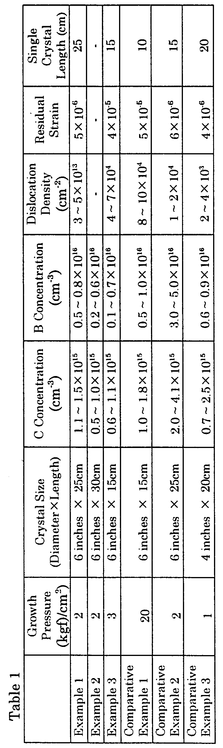
- Si doped GaAs was grown by the VGF method under the pressure of 2 atm of N2 gas using an airtight reactor tube of silicon carbide of high purity. As a result, a single crystal with 20 cm in length and 3 inches in diameter was obtained.
- The purity of the obtained crystal was analyzed. It is found that over the entire crystal, the concentration of all the impurities including carbon was not more than 5 × 1014 cm-3 except for Si. The obtained crystal was extremely high in purity.
- Undoped GaAs was grown by the VGF method under the N2 gas pressure of 1.2 atm using a reactor tube of a composite material having the surface of a base of graphite coated with silicon carbide to a thickness of 50 µm. It was confirmed that the reactor tube had the sufficient airtightness with the arrived degree of vacuum of not more than 1 × 10⁻²Torr. As a result, a single crystal of 30 cm in length and 3 inches in diameter was obtained.
- The purity of the obtained crystal was analyzed: It was found that, over the entire crystal, the carbon concentration was 1 ~ 2 × 1015cm-3, and the concentration of the other impurities was not more than 5 X 1014cm-3. The resistivity was 1 ~ 3 × 10⁷Ωcm. Thus, a GaAs crystal of extremely favorable semi-insulating property was obtained.
- A Si doped GaAs was grown by the VGF method under the Ar gas pressure of 1.5 atm using a reactor tube formed of a composite material having the surface of a base of porous mullite of low purity coated with aluminum oxide of high purity to a thickness of 100 µm. It was confirmed that the reactor tube had sufficient airtightness with the arrived degree of vacuum of not more than 1 × 10⁻³ Torr. As a result, a single crystal of 3 inches in diameter and 15 cm in length was obtained.
- The purity of the obtained crystal was analyzed. The concentration of all the impurities including carbon was not more than 5 × 1014cm-3 except for Si over the entire crystal. Thus, the purity was extremely high.
- Although the present invention has been described and illustrated in detail, it is clearly understood that the same is by way of illustration and example only and is not to be taken by way of limitation, the spirit and scope of the present invention being limited only by the terms of the appended claims.
Claims (17)
- An apparatus of producing a semiconductor crystal (50), comprising:a reactor tube (1) having an open end in at least one end side, formed of any one material selected from the group consisting of silicon carbide, silicon nitride, aluminum nitride, and aluminum oxide, or of a composite material with any one material selected from the group consisting of silicon carbide, silicon nitride, aluminum nitride, boron nitride, aluminum oxide, magnesium oxide, mullite, and carbon as a base, and having an oxidation-proof or airtight film formed on a surface of the base,heat means (3) arranged around said reactor tube (1) in the atmosphere,a flange (9) attached at said open end to seal said reactor tube (1), anda crucible (2) mounted in said reactor tube (1) to store a material of said semiconductor crystal.
- An apparatus of producing a semiconductor crystal (50), comprising:a reactor tube (1) having an open end in at least one end side, and formed of any one material selected from the group consisting of silicon carbide, silicon nitride, aluminum nitride, and aluminum oxide, or of a composite material with any one of the material selected from the group consisting of silicon carbide, silicon nitride, aluminum nitride, boron nitride, aluminum oxide, magnesium oxide, mullite, and carbon as a base, and having an oxidation-proof or airtight film formed on a surface of the base,heat means (3) arranged around said reactor tube (1) in the atmosphere,a flange (9) attached at said open end to seal said reactor tube (1),a crucible (2) mounted in said reactor tube (1) to store a material of said semiconductor crystal,a seal member (12) to seal a junction between said flange (9) and the open end of said reactor tube (1), andseal maintain means for maintaining a temperature of the junction between said flange (9) and the open end of said reactor tube (1) so as to maintain sealing function by said seal member (12).
- The apparatus of producing a semiconductor crystal according to claim 2, wherein said seal maintain means comprises provision of a heat insulator (8) between a heating portion of said reactor tube (1) by said heat means (3) and a junction between said flange (9) and the open end of said reactor tube (1).
- The method of producing a semiconductor crystal according to claim 2, wherein said seal maintain means comprises circulation of cooling water within a jacket attached to said flange (9).
- The apparatus of producing a semiconductor crystal according to claim 2, wherein said seal maintain means comprises cooling by air a junction between said flange (9) and the open end of said reactor tube (1).
- The apparatus of producing a semiconductor crystal according to claim 2, further comprising a shaft member (4) connected to said crucible (2) via said flange (9).
- The apparatus of producing a semiconductor crystal according to claim 6, wherein said reactor tube (1) is used arranged in a vertical direction, and
wherein said shaft member (4) can move said crucible (2) mounted in said reactor tube (1) upwards and downwards. - The method of producing a semiconductor crystal according to claim 2, further comprising at least one temperature measurement means (13) in proximity to said crucible (2) via said flange (9).
- The apparatus of producing a semiconductor crystal according to any of claims 1-8, wherein said semiconductor crystal (50) is a GaAs crystal.
- The apparatus of producing a semiconductor crystal according to claim 9, wherein pressure inside said reactor tube (1) is maintained to be higher than the atmospheric pressure, and pressure outside said reactor tube (1) is the atmospheric pressure.
- The apparatus of producing a semiconductor crystal according to claim 9, further comprising a reservoir (6) in said reactor tube (1) to store a second material (80) of said semiconductor crystal (50),
wherein said reservoir includes a pipe (7) to introduce gas of said second material (80) into said crucible (2). - The apparatus of producing a semiconductor crystal according to claim 11, wherein the material stored in said crucible (2) is Ga, and the second material (80) stored in said reservoir (6) is As.
- A method of producing a semiconductor crystal (50) , comprising the steps of:mounting a crucible (2) storing material of said semiconductor crystal in a reactor tube (1) having an open end in at least one end side, and formed of any one material selected from the group consisting of silicon carbide, silicon nitride, aluminum nitride, and aluminum oxide, or of a composite material with any one material selected from the group consisting of silicon carbide, silicon nitride, aluminum nitride, boron nitride, aluminum oxide, magnesium oxide, mullite, and carbon as a base, and having an oxidation-proof or airtight film formed on a surface of the base,attaching a flange (9) at said open end to seal said reactor tube (1),maintaining interior of said reactor tube under inert gas atmosphere,forming material melt (60) by heat means (3) arranged around said reactor tube (1) in the atmosphere, andgrowing said semiconductor crystal (50) by solidifying said material melt (60).
- The method of producing a semiconductor crystal according to claim 13, wherein said semiconductor crystal (50) is a GaAs crystal,
wherein the step of mounting a crucible (2) storing the material of a semiconductor crystal in said reactor tube (1) comprises the steps offilling said crucible (2) with Ga,filling a reservoir (6) with As (80), said reservoir including a pipe (7),mounting said crucible (2) filled with Ga and said reservoir (6) filled with said As (80) in said reactor tube (1), and
wherein said step of forming material melt (60) comprises the steps ofheating the GA in said crucible (2) up to a temperature higher than the melting point of GaAs by said heat means (3),heating and sublimating the As (80) in said reservoir (2) by said heat means (3) to produce arsenic vapor, andintroducing said produced arsenic vapor into said Ga via said pipe (7) to form GaAs melt (60) in said crucible (2). - The method of producing a semiconductor crystal according to claim 13 or 14, wherein said step of growing a semiconductor crystal (50) uses any crystal growth method selected from the group consisting of a VB method, a VGF method, and a pulling method.
- A semiconductor crystal (50) of a compound, characterized in that the diameter is at least 6 inches, and the average dislocation density is not more than 1 × 104cm-2.
- A semiconductor crystal substrate of a compound, characterized in that the diameter is at least 6 inches, and the average dislocation density is not more than 1 × 104cm-2.
Priority Applications (2)
| Application Number | Priority Date | Filing Date | Title |
|---|---|---|---|
| EP07021740A EP1895025B1 (en) | 1997-12-26 | 1998-12-22 | Method and apparatus of production of a semiconductor crystal |
| EP08005885A EP1939332A1 (en) | 1997-12-26 | 1998-12-22 | Semiconductor crystal, and method and apparatus of production |
Applications Claiming Priority (6)
| Application Number | Priority Date | Filing Date | Title |
|---|---|---|---|
| JP36009097 | 1997-12-26 | ||
| JP36009097 | 1997-12-26 | ||
| JP7296998 | 1998-03-23 | ||
| JP7296998 | 1998-03-23 | ||
| JP35255798 | 1998-12-11 | ||
| JP35255798A JP4135239B2 (en) | 1997-12-26 | 1998-12-11 | Semiconductor crystal, manufacturing method thereof and manufacturing apparatus |
Related Child Applications (2)
| Application Number | Title | Priority Date | Filing Date |
|---|---|---|---|
| EP07021740A Division EP1895025B1 (en) | 1997-12-26 | 1998-12-22 | Method and apparatus of production of a semiconductor crystal |
| EP08005885A Division EP1939332A1 (en) | 1997-12-26 | 1998-12-22 | Semiconductor crystal, and method and apparatus of production |
Publications (2)
| Publication Number | Publication Date |
|---|---|
| EP0927777A1 true EP0927777A1 (en) | 1999-07-07 |
| EP0927777B1 EP0927777B1 (en) | 2008-07-16 |
Family
ID=27301090
Family Applications (3)
| Application Number | Title | Priority Date | Filing Date |
|---|---|---|---|
| EP98124552A Expired - Lifetime EP0927777B1 (en) | 1997-12-26 | 1998-12-22 | Method and apparatus of production of semiconductor crystal |
| EP08005885A Ceased EP1939332A1 (en) | 1997-12-26 | 1998-12-22 | Semiconductor crystal, and method and apparatus of production |
| EP07021740A Expired - Lifetime EP1895025B1 (en) | 1997-12-26 | 1998-12-22 | Method and apparatus of production of a semiconductor crystal |
Family Applications After (2)
| Application Number | Title | Priority Date | Filing Date |
|---|---|---|---|
| EP08005885A Ceased EP1939332A1 (en) | 1997-12-26 | 1998-12-22 | Semiconductor crystal, and method and apparatus of production |
| EP07021740A Expired - Lifetime EP1895025B1 (en) | 1997-12-26 | 1998-12-22 | Method and apparatus of production of a semiconductor crystal |
Country Status (4)
| Country | Link |
|---|---|
| US (1) | US6254677B1 (en) |
| EP (3) | EP0927777B1 (en) |
| JP (1) | JP4135239B2 (en) |
| DE (2) | DE69840840D1 (en) |
Cited By (7)
| Publication number | Priority date | Publication date | Assignee | Title |
|---|---|---|---|---|
| EP0947609A2 (en) * | 1998-03-25 | 1999-10-06 | Sumitomo Electric Industries, Ltd. | Method of preparing a compound semiconductor crystal and compound semiconductor crystal |
| EP0990717A1 (en) * | 1998-09-28 | 2000-04-05 | Sumitomo Electric Industries, Ltd. | GaAs single crystal substrate and epitaxial wafer using the same |
| EP1740331B1 (en) * | 2004-04-13 | 2009-07-29 | Helmholtz-Zentrum Berlin für Materialien und Energie GmbH | Method and arrangement for crystal growth from fused metals or fused solutions |
| US7838392B2 (en) | 2002-06-07 | 2010-11-23 | Taiwan Semiconductor Manufacturing Company, Ltd. | Methods for forming III-V semiconductor device structures |
| EP2510138A2 (en) * | 2009-12-13 | 2012-10-17 | Axt, Inc. | Germanium ingots/wafers having low micro-pit density (mpd) as well as systems and methods for manufacturing same |
| CN101736401B (en) * | 2008-11-10 | 2013-07-24 | Axt公司 | Method and device for growing germanium crystal |
| CN109252220A (en) * | 2018-12-04 | 2019-01-22 | 中国电子科技集团公司第四十六研究所 | A kind of VGF/VB arsenide gallium monocrystal furnace structure and growing method |
Families Citing this family (12)
| Publication number | Priority date | Publication date | Assignee | Title |
|---|---|---|---|---|
| JP3019205U (en) * | 1994-12-19 | 1995-12-12 | ぢどり亭株式会社 | Charcoal grilling equipment |
| US6572700B2 (en) * | 1997-12-26 | 2003-06-03 | Sumitomo Electric Industries, Ltd. | Semiconductor crystal, and method and apparatus of production thereof |
| JP4416040B2 (en) * | 1997-12-26 | 2010-02-17 | 住友電気工業株式会社 | Compound semiconductor crystal |
| JP2002121100A (en) * | 2000-10-10 | 2002-04-23 | Dowa Mining Co Ltd | Method of producing semiconductor single crystal |
| JP4276627B2 (en) * | 2005-01-12 | 2009-06-10 | ソルボサーマル結晶成長技術研究組合 | Pressure vessel for single crystal growth and method for producing the same |
| JP4513638B2 (en) * | 2005-04-18 | 2010-07-28 | 住友電気工業株式会社 | Compound semiconductor crystal manufacturing equipment |
| CA2510415C (en) * | 2005-06-21 | 2012-08-14 | Redlen Technologies Inc. | A cold-walled vessel process for compounding, homogenizing and consolidating semiconductor compounds |
| WO2010072706A1 (en) * | 2008-12-22 | 2010-07-01 | Shell Internationale Research Maatschappij B.V. | Process and reactor system for the preparation of an olefinic product |
| KR101353679B1 (en) * | 2012-05-04 | 2014-01-21 | 재단법인 포항산업과학연구원 | Apparatus for growing large diameter single crystal and method for growing using the same |
| US10633759B2 (en) * | 2013-09-30 | 2020-04-28 | Gtat Corporation | Technique for controlling temperature uniformity in crystal growth apparatus |
| US10815586B2 (en) | 2017-09-14 | 2020-10-27 | Sumitomo Electric Industries, Ltd. | Gallium-arsenide-based compound semiconductor crystal and wafer group |
| CN111406130B (en) * | 2018-02-23 | 2021-10-15 | 住友电气工业株式会社 | Gallium arsenide crystal substrate |
Citations (6)
| Publication number | Priority date | Publication date | Assignee | Title |
|---|---|---|---|---|
| FR2535312A1 (en) * | 1982-10-28 | 1984-05-04 | Toshiba Ceramics Co | MOLDED ELEMENT BASED ON SILICON CARBIDE FOR USE IN THE MANUFACTURE OF SEMICONDUCTORS |
| EP0290322A1 (en) * | 1987-04-27 | 1988-11-09 | Societe Europeenne De Propulsion | Composite material cartridge for a single crystal-producing apparatus |
| GB2205087A (en) * | 1987-04-28 | 1988-11-30 | Furukawa Electric Co Ltd | Method and apparatus for manufacture of single crystal semiconductor compound |
| JPH02233578A (en) * | 1989-03-06 | 1990-09-17 | Mitsubishi Metal Corp | Treating device of compound semiconductor having high dissociation pressure and treating method |
| EP0559921A1 (en) * | 1991-09-19 | 1993-09-15 | Mitsubishi Materials Corporation | Apparatus for and method of producing single crystal semiconductor of high dissociation pressure compound |
| JPH07221038A (en) * | 1994-02-04 | 1995-08-18 | Matsushita Electron Corp | Heat treating furnace |
Family Cites Families (12)
| Publication number | Priority date | Publication date | Assignee | Title |
|---|---|---|---|---|
| US3615878A (en) * | 1970-01-30 | 1971-10-26 | Westinghouse Electric Corp | Process for the thermal treatment of a semiconductor material having a volatile component |
| CA956867A (en) | 1970-12-04 | 1974-10-29 | Albert G. Fischer | Method and apparatus for forming crystalline bodies of a semiconductor material |
| JPS55140792A (en) | 1979-04-16 | 1980-11-04 | Nippon Telegr & Teleph Corp <Ntt> | Manufacture of 3-5 group compound semiconductor single crystal |
| US4404172A (en) * | 1981-01-05 | 1983-09-13 | Western Electric Company, Inc. | Method and apparatus for forming and growing a single crystal of a semiconductor compound |
| JPS58181799A (en) * | 1982-04-16 | 1983-10-24 | Nippon Telegr & Teleph Corp <Ntt> | Manufacture of gaas single crystal containing boron |
| DE3472577D1 (en) * | 1983-08-31 | 1988-08-11 | Japan Res Dev Corp | Apparatus for growing single crystals of dissociative compounds |
| JPS60255689A (en) * | 1984-05-30 | 1985-12-17 | Fujitsu Ltd | Production of semiconductor crystal |
| JPH0218375A (en) | 1988-07-07 | 1990-01-22 | Toshiba Ceramics Co Ltd | Device for pulling up semiconductor single crystal |
| KR930005015B1 (en) * | 1990-04-04 | 1993-06-11 | 한국과학기술연구원 | Apparatus for growing of single-crystal |
| DE19580737C2 (en) * | 1994-06-02 | 2002-02-21 | Kobe Steel Ltd | Method and device for producing connecting single crystals |
| JP3260568B2 (en) * | 1994-10-31 | 2002-02-25 | 株式会社神戸製鋼所 | Crucible for compound semiconductor production |
| JP3201305B2 (en) * | 1996-04-26 | 2001-08-20 | 住友電気工業株式会社 | Method for producing group III-V compound semiconductor crystal |
-
1998
- 1998-12-11 JP JP35255798A patent/JP4135239B2/en not_active Expired - Lifetime
- 1998-12-21 US US09/217,349 patent/US6254677B1/en not_active Expired - Lifetime
- 1998-12-22 DE DE69840840T patent/DE69840840D1/en not_active Expired - Lifetime
- 1998-12-22 EP EP98124552A patent/EP0927777B1/en not_active Expired - Lifetime
- 1998-12-22 EP EP08005885A patent/EP1939332A1/en not_active Ceased
- 1998-12-22 EP EP07021740A patent/EP1895025B1/en not_active Expired - Lifetime
- 1998-12-22 DE DE69839723T patent/DE69839723D1/en not_active Expired - Lifetime
Patent Citations (6)
| Publication number | Priority date | Publication date | Assignee | Title |
|---|---|---|---|---|
| FR2535312A1 (en) * | 1982-10-28 | 1984-05-04 | Toshiba Ceramics Co | MOLDED ELEMENT BASED ON SILICON CARBIDE FOR USE IN THE MANUFACTURE OF SEMICONDUCTORS |
| EP0290322A1 (en) * | 1987-04-27 | 1988-11-09 | Societe Europeenne De Propulsion | Composite material cartridge for a single crystal-producing apparatus |
| GB2205087A (en) * | 1987-04-28 | 1988-11-30 | Furukawa Electric Co Ltd | Method and apparatus for manufacture of single crystal semiconductor compound |
| JPH02233578A (en) * | 1989-03-06 | 1990-09-17 | Mitsubishi Metal Corp | Treating device of compound semiconductor having high dissociation pressure and treating method |
| EP0559921A1 (en) * | 1991-09-19 | 1993-09-15 | Mitsubishi Materials Corporation | Apparatus for and method of producing single crystal semiconductor of high dissociation pressure compound |
| JPH07221038A (en) * | 1994-02-04 | 1995-08-18 | Matsushita Electron Corp | Heat treating furnace |
Non-Patent Citations (4)
| Title |
|---|
| KAWASE T ET AL: "LOW DISLOCATION DENSITY 6-INCH DIAMETER GAAS SINGLE CRYSTALS GROWN BY THE VCZ METHOD", GALLIUM ARSENIDE AND RELATED COMPOUNDS, KARUIZAWA, SEPT. 28 - OCT. 2, 1992, no. SYMP. 19, 28 September 1992 (1992-09-28), IKEGAMI T;HASEGAWA F; TAKEDA Y, pages 13 - 18, XP000366193 * |
| KUMA S ET AL: "GROWTH AND CHARACTERIZATION OF HUGE GAAS CRYSTALS", GALLIUM ARSENIDE AND RELATED COMPOUNDS, FREIBURG, AUG. 29 - SEPT. 2, 1993, no. SYMP. 20, 29 August 1993 (1993-08-29), RUPPRECHT H S;WEIMANN G, pages 497 - 504, XP000478980 * |
| PATENT ABSTRACTS OF JAPAN vol. 014, no. 544 (C - 0784) 4 December 1990 (1990-12-04) * |
| PATENT ABSTRACTS OF JAPAN vol. 095, no. 011 26 December 1995 (1995-12-26) * |
Cited By (14)
| Publication number | Priority date | Publication date | Assignee | Title |
|---|---|---|---|---|
| USRE42279E1 (en) * | 1998-03-25 | 2011-04-12 | Sumitomo Electric Industries, Ltd. | Method of preparing a compound semiconductor crystal |
| EP0947609A3 (en) * | 1998-03-25 | 2002-02-06 | Sumitomo Electric Industries, Ltd. | Method of preparing a compound semiconductor crystal and compound semiconductor crystal |
| US6485563B2 (en) | 1998-03-25 | 2002-11-26 | Sumitomo Electric Industries, Ltd. | Method of preparing a compound semiconductor crystal |
| USRE40662E1 (en) * | 1998-03-25 | 2009-03-17 | Sumitomo Electric Industries, Ltd. | Method of preparing a compound semiconductor crystal |
| EP0947609A2 (en) * | 1998-03-25 | 1999-10-06 | Sumitomo Electric Industries, Ltd. | Method of preparing a compound semiconductor crystal and compound semiconductor crystal |
| EP0990717A1 (en) * | 1998-09-28 | 2000-04-05 | Sumitomo Electric Industries, Ltd. | GaAs single crystal substrate and epitaxial wafer using the same |
| US6180269B1 (en) | 1998-09-28 | 2001-01-30 | Sumitomo Electric Industries, Ltd. | GaAs single crystal substrate and epitaxial wafer using the same |
| US7838392B2 (en) | 2002-06-07 | 2010-11-23 | Taiwan Semiconductor Manufacturing Company, Ltd. | Methods for forming III-V semiconductor device structures |
| EP1740331B1 (en) * | 2004-04-13 | 2009-07-29 | Helmholtz-Zentrum Berlin für Materialien und Energie GmbH | Method and arrangement for crystal growth from fused metals or fused solutions |
| US8506706B2 (en) | 2008-11-08 | 2013-08-13 | Axt, Inc | Systems, methods and substrates of monocrystalline germanium crystal growth |
| CN101736401B (en) * | 2008-11-10 | 2013-07-24 | Axt公司 | Method and device for growing germanium crystal |
| EP2510138A2 (en) * | 2009-12-13 | 2012-10-17 | Axt, Inc. | Germanium ingots/wafers having low micro-pit density (mpd) as well as systems and methods for manufacturing same |
| EP2510138A4 (en) * | 2009-12-13 | 2014-09-03 | Axt Inc | Germanium ingots/wafers having low micro-pit density (mpd) as well as systems and methods for manufacturing same |
| CN109252220A (en) * | 2018-12-04 | 2019-01-22 | 中国电子科技集团公司第四十六研究所 | A kind of VGF/VB arsenide gallium monocrystal furnace structure and growing method |
Also Published As
| Publication number | Publication date |
|---|---|
| DE69839723D1 (en) | 2008-08-28 |
| DE69840840D1 (en) | 2009-06-25 |
| EP1895025A2 (en) | 2008-03-05 |
| EP1895025B1 (en) | 2009-05-13 |
| JPH11335194A (en) | 1999-12-07 |
| EP1895025A3 (en) | 2008-05-21 |
| EP0927777B1 (en) | 2008-07-16 |
| EP1939332A1 (en) | 2008-07-02 |
| US6254677B1 (en) | 2001-07-03 |
| JP4135239B2 (en) | 2008-08-20 |
Similar Documents
| Publication | Publication Date | Title |
|---|---|---|
| US6866714B2 (en) | Large size semiconductor crystal with low dislocation density | |
| US6254677B1 (en) | Semiconductor crystal, and method and apparatus of production thereof | |
| EP0068021B1 (en) | The method and apparatus for forming and growing a single crystal of a semiconductor compound | |
| US4874458A (en) | Single crystal growing method having improved melt control | |
| EP0140509A1 (en) | An lec method and apparatus for growing single crystal | |
| US20030037721A1 (en) | Method and apparatus for growing semiconductor crystals with a rigid support with carbon doping and resistivity control and thermal gradient control | |
| JP4416040B2 (en) | Compound semiconductor crystal | |
| US5041186A (en) | Method for manufacturing compound semiconductor single crystals using a hydrogen monitor gas | |
| EP0244987B1 (en) | A process for growing a multi-component crystal | |
| JP2008239480A5 (en) | ||
| US4654110A (en) | Total immersion crystal growth | |
| EP0210439B1 (en) | Method for growing single crystals of dissociative compound semiconductor | |
| US5493985A (en) | Process and apparatus for controlled synthesis and in-situ single crystal growth of phosphorus compounds and the crystals therefrom | |
| US5656079A (en) | Statement of government interest | |
| JP2003206200A (en) | p-TYPE GaAs SINGLE CRYSTAL AND METHOD FOR PRODUCING THE SAME | |
| JPH11147785A (en) | Production of single crystal | |
| JP2002255697A (en) | GALLIUM-ARSENIC SINGLE CRYSTAL AND GaAs WAFER AND PRODUCTION METHOD FOR GaAs SINGLE CRYSTAL | |
| JP3569954B2 (en) | Semiconductor crystal growth method | |
| JPH09142995A (en) | Production of p-type single crystal silicon carbide | |
| JP3154351B2 (en) | Single crystal growth method | |
| Szeles et al. | Advances in the crystal growth of semiinsulating CdZnTe for radiation detector applications | |
| JP2885452B2 (en) | Boat growth method for group III-V compound crystals | |
| JPH0193497A (en) | Production of znse single crystal | |
| JPH01122995A (en) | Growth of compound semiconductor single crystal | |
| JP2005132717A (en) | Compound semiconductor single crystal and its manufacturing method |
Legal Events
| Date | Code | Title | Description |
|---|---|---|---|
| PUAI | Public reference made under article 153(3) epc to a published international application that has entered the european phase |
Free format text: ORIGINAL CODE: 0009012 |
|
| AK | Designated contracting states |
Kind code of ref document: A1 Designated state(s): DE FR GB |
|
| AX | Request for extension of the european patent |
Free format text: AL;LT;LV;MK;RO;SI |
|
| 17P | Request for examination filed |
Effective date: 19990608 |
|
| AKX | Designation fees paid |
Free format text: DE FR GB |
|
| 17Q | First examination report despatched |
Effective date: 20021219 |
|
| GRAP | Despatch of communication of intention to grant a patent |
Free format text: ORIGINAL CODE: EPIDOSNIGR1 |
|
| RTI1 | Title (correction) |
Free format text: METHOD AND APPARATUS OF PRODUCTION OF SEMICONDUCTOR CRYSTAL |
|
| GRAS | Grant fee paid |
Free format text: ORIGINAL CODE: EPIDOSNIGR3 |
|
| GRAA | (expected) grant |
Free format text: ORIGINAL CODE: 0009210 |
|
| AK | Designated contracting states |
Kind code of ref document: B1 Designated state(s): DE FR GB |
|
| REG | Reference to a national code |
Ref country code: GB Ref legal event code: FG4D |
|
| REF | Corresponds to: |
Ref document number: 69839723 Country of ref document: DE Date of ref document: 20080828 Kind code of ref document: P |
|
| PLBE | No opposition filed within time limit |
Free format text: ORIGINAL CODE: 0009261 |
|
| STAA | Information on the status of an ep patent application or granted ep patent |
Free format text: STATUS: NO OPPOSITION FILED WITHIN TIME LIMIT |
|
| 26N | No opposition filed |
Effective date: 20090417 |
|
| PGFP | Annual fee paid to national office [announced via postgrant information from national office to epo] |
Ref country code: GB Payment date: 20091216 Year of fee payment: 12 Ref country code: FR Payment date: 20091221 Year of fee payment: 12 |
|
| GBPC | Gb: european patent ceased through non-payment of renewal fee |
Effective date: 20101222 |
|
| REG | Reference to a national code |
Ref country code: FR Ref legal event code: ST Effective date: 20110831 |
|
| PG25 | Lapsed in a contracting state [announced via postgrant information from national office to epo] |
Ref country code: FR Free format text: LAPSE BECAUSE OF NON-PAYMENT OF DUE FEES Effective date: 20110103 |
|
| PG25 | Lapsed in a contracting state [announced via postgrant information from national office to epo] |
Ref country code: GB Free format text: LAPSE BECAUSE OF NON-PAYMENT OF DUE FEES Effective date: 20101222 |
|
| PGFP | Annual fee paid to national office [announced via postgrant information from national office to epo] |
Ref country code: DE Payment date: 20121219 Year of fee payment: 15 |
|
| REG | Reference to a national code |
Ref country code: DE Ref legal event code: R119 Ref document number: 69839723 Country of ref document: DE |
|
| REG | Reference to a national code |
Ref country code: DE Ref legal event code: R119 Ref document number: 69839723 Country of ref document: DE Effective date: 20140701 |
|
| PG25 | Lapsed in a contracting state [announced via postgrant information from national office to epo] |
Ref country code: DE Free format text: LAPSE BECAUSE OF NON-PAYMENT OF DUE FEES Effective date: 20140701 |