Background of the invention:
1.Field of the invention
-
The present invention relates to a PC card detachably
installed and used for information processing devices, such as a
personal computer or a digital-still-camera, to process a variety
of information.
2.Description of the Related Art
-
A PC card is detachably installed and used for information
processing devices, such as a personal computer (an abbreviated
name "PC" is used hereinafter) or a digital-still-camera, to
process a variety of information of characters, voices or images,
and also used for an increase in ability of a variety of processes
and an expansion in processing function for the information
processing devices.
-
Originally, the PC card has been internationally
standardized based on a unified standard (PC Card Standard)
published by the PCMCIA (the Personal Computer Memory Card
International Association) which is an association established to
form a card device standard for the PC, and utilized mainly for
a portable compact PC such as a notebook PC or PDA. Physical
specification (a visual shape) of the PC card is a card type with
a length of 85.6 mm and a width of 54.0 mm and classified in type
I, type II and type III depending on the difference of thickness.
A two-piece connector with 68 pins is used for a PC card connector.
The PC card is used by inserting the connector in a PC card slot
of a PC card interface provided in the portable PC and the like
and can be pulled up from the PC card slot when it is not used.
-
Thus, Since the PC card is easily detachable and superior
in portability due to its compact size, the application has been
spreading not only to a semiconductor memory card as an auxiliary
storage, but also to the auxiliary storage having a hard disk device
such as a magnetic disk, and to the related field of communication
and network such as a modem function or a LAN function (Local Area
Network). Further, the field of application for the use of the PC
card has been spreading without being limited to the portable
compact PC. For example, by being used for a digital image
information processing device such as a digital-still-camera, the
PC card is used as a image storage detachable and superior in
portability or as a data transfer device (for example: a LAN card
or a Modem card) to transfer the memorized images in the camera
to the PC and the like.
-
Conventionally, it has been required to install an extension
board with a predetermined function in an extension bus slot or
to install an internal substrate module connecting to the mother
board of the PC to provide a desired processing ability or
processing function to the information processing device, so
involving difficulties in exchange and portability of the
substrate. However, with the PC card, the desired processing
ability and function are instantly provided by exchanging the PC
card to insert in the slot, therefore providing an advantage of
easiness in handling. It should be noted that there are several
methods such as pulling and inserting or placing to cramp for
attaching/detaching the PC card to/from the information processing
device.
-
Recently, along with the development of high integration
technology of semiconductor devices, the development of the
information processing devices including a more compact PC,
digital-still-camera, digital video camera, or commercial
equipment such as portable audio equipment results in a demand for
the emergence of the more compact PC card, in addition to the
emergence for the conventional PC card based on the PCMCIA standard
intended for the use of the portable PC. Therefore, the following
standards for the compact memory card are proposed and actually
appear in the market as products.
-
The first standard is the "Compact Flash (the registered
trademark of SanDisk Corporation)" proposed by the CFA (Compact
Flash Association). It is a compact flash memory card with
approximately 8 MB in capacity having an outside dimension of 36.4
x 42.8 x 3.3 mm3. The second standard is the "Small PC Card" proposed
by Matsushita Battery Industrial Co., Ltd., the JEIDA (the Japan
Electronic Industry Development Association) and the PCMCIA,
having an outside dimension of 45.0 x 42.8 x 5.0 mm3 with
approximately a half-length of the conventional PC card. The third
standard is the "Miniature Card" proposed by the Miniature Card
Implementers Forum and the PCMCIA, with an outer dimension of 38
x 33 x 3.5 mm3.
-
The fourth standard is the "SmartMedia (the registered
trademark of Toshiba Corporation)" by the SSFDC Forum. This is a
flash EEPROM card with a capacity of approximately 2∼16 MB having
an outside dimension of 37 x 45 x 0.67 mm3. The fifth standard
is the "MMC (MultiMedia card)" proposed by the MultiMedia Card
Association. This is a flash EEPROM card with, for example,
approximately 10 MB in capacity having an outside dimension of 24
x 32 x 1.4mm3. A sixth standard is the "Memory Stick (the trademark
of Sony Corporation)" proposed by Sony Corporation. This is an
EEPROM with, for example, a capacity of approximately 8 MB having
an outside dimension of 21.5 x 50 x 2.8 mm3. Moreover, a compact
PC card with a hard disk drive using magnetic storage is also
developed. In this application, each of the compact cards having
the aforementioned functions including the similar cards is
generally named a PC card.
-
The object of the PC card is to solve the problems regarding
the insufficiency of compatibility among the IC cards as well as
the limitation of the extension of the use and the function, which
have been in the past owned by the IC card used mainly for the purpose
of exchange of a card having magnetic stripes, and further the PC
card is realized by newly forming physical specification, electric
specification and software specification to extend the processing
ability and processing function of the PC and the like. In short,
though the PC card has its origin in an IC memory card, it is
significantly different from the IC memory card in mechanism and
application. Furthermore, it can be referred as an extended
function card standardized and realized by electric specification
and software specification which are strongly influenced by a PC
extension bus architecture. Thus, the application field and
technical field are new industrial utility and technical fields
which can provide functions far beyond the range of the market
intended originally in the IC card.
Summary of the invention:
-
As has been previously described, the PC card exhibits the
predetermined functions by being inserted in the slot of the PC
card interface provided in the information processing device such
as the PC and digital-still-camera. And a method to use the PC card
in the information processing device which is, for example, not
ordinarily equipped with the PC card interface like a host computer
system which does not have a portability as a desktop, is described
bellow.
-
For example, Japanese Laid-open Patent Application No.7-302140
discloses to make the PC card function from the information
processing device by preparing a PC card interface unit having an
PC card interface therein, connecting the unit to the information
processing device, and inserting the PC card in the slot installed
in the PC card interface.
-
Currently, there are already several PC card interface units
connectable to the desktop PC, such as a type using a parallel port
equipped as a standard in the PC, a PC card drive device with the
SCSI (Small Computer System Interface) connection, or a PC card
drive device using a dedicated interface board by inserting in a
PCI slot of the PC. Though the PC card drive device having a parallel
port connection or the SCSI connection can mainly use only a memory
card among the PC cards, the drive device using the dedicated
interface can basically use all kinds of PC cards as is the case
of the PC card interface equipped as a standard in the portable
compact PC.
-
Thus, the PC card drive device is required to be built in
the information processing drive to use the PC card in the
information processing device not equipped with the PC card
interface, therefore producing some problems. First problem is
that advantages originally owned by the PC card to be easily
detachable, flexible and compact are restricted. For example,
after removing the PC card (memory card) having data recorded by
a information processing device (a) equipped with the PC card
interface from the information processing device (a) and then
carrying it, when the contents in the PC card is attempted to be
read by a information processing device (b) at another location,
the contents recorded in the PC card can not naturally be read unless
the PC card drive device is equipped in the information processing
device (b). Though it is possible to carry the PC card drive device
together with the PC card to avoid above disadvantages, it extremely
damages the portability of the PC card.
-
On the other hand, the portability can be ensured by
installing the PC card drive device in the information processing
device (b) beforehand because only the transfer is required.
However, when there are a plurality of the information processing
devices (b), the installation of the PC card drive device to each
information processing device (b) is required, and therefore the
second problem being high cost and not economical is produced.
-
Further, since the installation of the dedicated driver
software and the setting of boards are required to introduce the
PC card drive device in the information processing device (b), the
third problem being bothered with maintenance control of the
information processing device is produced.
-
It is a principal object of the present invention to provide
a PC card connectable to a plurality of information processing
devices without losing the advantages being easily detachable,
flexible, and portable originally owned by the PC card.
-
Another object of the present invention is to provide a PC
card connectable to the information processing device which does
not have the PC card drive device.
-
A further object of the present invention is to provide a
PC card connectable to an interface installed beforehand as a
standard in the information processing device.
-
The above objects are achieved by a PC card at least
comprising a function block providing a predetermined function for
the information processing device, a first interface section
transferring a data between the function block and the first
information processing device, and a second interface section
having a different specification from the first interface section
and transferring data between the function block and the second
information processing device.
-
In the PC card of the present invention, for example, if the
first interface section is designed to correspond to the existing
PC card interface and the second interface section is structured
to correspond to a interface which has a different specification
from the PC card interface such as the USB interface, the PC card
of the present invention can be used, without the connection of
the PC card drive device, not only for the first information
processing device having a connector for the PC card such a portable
PC and digital camera but also for the second information processing
device which ordinary does not have a connector for the PC card
such as the desktop PC, therefore leading to an increase in
portability and flexibility originally owned by the PC card. It
should be noted that "transfer data" in this application does not
mean only data which should be stored but also the data transmission
of a wide variety of concepts including addresses, commands to the
PC card, or request signals and the like sent from the PC card to
the information processing device.
-
In the PC card of the present invention, the first interface
section comprises the first physical layer interface physically
connecting to the first information processing device, and the
first interface control section arranged between the first
physical layer interface and the function block. Further, the first
interface section comprises a first supplementary circuit to
realize a control procedure through the first interface control
section between the first information processing device and
function block. Furthermore, the first supplementary circuit is
arranged between the function block and the first interface control
section.
-
Also, in the PC card of the present invention, the second
interface section comprises the second physical layer interface
physically connecting to the second information processing device,
and the second interface control section arranged between the
second physical layer interface and the function block. The second
interface section comprises the second supplementary circuit for
realizing the control procedure through the second interface
control section between the second information processing device
and the function block. Further, the second supplementary circuit
is arranged between the function block and the second interface
control section.
-
In the PC card of the present invention, a plurality of signal
lines are connected from the function block to the first and second
interface sections, and at least a part of the signal lines is
connected to both of the first signal lines connecting to the first
interface section and second signal lines connecting to the second
interface section, through the junction section as common lines.
The common lines are data or address bus lines where the data signals
or address signals which should be transferred between the first
and second information processing device and the function block
flow.
-
Thus, in the present invention, a part of a plurality of the
signal lines connected from the function block to the first and
second interface sections is, as the common signal lines, connected
to both of the first interface section and the second interface
section through the junction, thereby realizing a PC card having
a plurality of kinds of interfaces in a simple circuit structure.
Further, the first and second supplementary circuits have
functions to take out the control commands, data and the like for
the function block from data received from the first or second
interface control section, or to convert the data and control
information received from the function block to the format of the
first or second interface control section. Further, the first or
second supplementary circuit has functions to absorb a difference
of speed between the first or second control section and the
function block with buffer processing or WAIT operation, or to
convert a difference in bus signal formats between the first or
second interface control section and the function block by a
parallel/serial converter and so on.
-
Furthermore, the PC card of the present invention comprises
a means for switching which selects one of the first and second
interface sections and connects the selected one to the function
block. The means for switching also comprised a signal line
switching section to electrically connect one of the first signal
lines and the second signal lines to the common signal lines.
Further, the signal switching section connects electrically the
common signal lines to only one of the first signal lines and second
signal lines, on the basis of a first power source voltage supplied
from the first information processing device to the first interface
section and a second power source voltage supplied from the second
information processing device to the second interface section.
Also, when both of the first power source voltage and the second
power source voltage are simultaneously supplied, the signal line
switching section comprises a switching circuit to select one of
the first signal lines or second signal lines to electrically
connect to the common signal lines. In the PC card of the present
invention, the signal line switching section sets one of the first
signal lines or the second signal lines, which is not electrically
connected to the common signal lines, relatively in the state of
a high impedance.
-
So, in the present invention, when data are transferred
between the function block and the first or second interface section
through the common signal lines, the signal lines on the side of
interface section which should be in a deactivated state without
data transfer can be maintained in the state of the high impedance,
therefore it is possible to easily and surely transfer the data
to be transferred to the signal lines between the side of the
interface section executing the data transfer and the function
block.
-
Further, since the signal line switching section has a
switching circuit to select one of the first signal lines or second
signal lines electrically connected to the common signal lines when
both of the first power source voltage and the second power source
voltage are supplied, data to the first and second information
processing device can be alternatively transferred by relatively
easy switching of the connection even if the PC card is connected
to both of the first and second information processing devices.
No problem is introduced even if the interface does not have a
dynamic means for setting of plug & play because recognition can
be made by a reset processing from software operating in the
information processing device.
-
Also, the PC card of the present invention comprises a power
source control circuit in which the means for switching controls
a voltage supplied to the first and second interface sections to
deactivate either one of the first or second interface sections.
-
According to the present invention, when the state, in which
each of the first and second interface sections are connected to
each of the first and second information processing devices,
arises, one of the interface sections is maintained in the activated
state and the other of the interface sections is maintained in the
high impedance state, therefore data to be transferred can be
transferred easily and surely when the data is transferred between
the side of the interface section in the high impedance state and
the function block.
-
Further, in the PC card of the present invention, the second
interface section corresponds to the USB standard. Or, the second
interface section corresponds to the IEEE1394 standard.
-
Also, in the PC card of the present invention, the function
block provides a data storage function to the first and second
information processing devices. Or the function block provides a
data communication function to the first and second information
processing devices.
Brief description of the drawings:
-
The present invention is further described in connection
with the accompanying drawings, in which:
- Fig.1 shows a schematic structure of the PC card in the first
embodiment of the present invention;
- Fig.2 shows a schematic structure of the PC card in the second
embodiment of the present invention;
- Fig.3 shows a schematic structure of the PC card in the third
embodiment of the present invention; and
- Fig.4 shows a schematic structure of the PC card in the fourth
embodiment of the present invention.
-
Description of the preferred embodiments:
First Embodiment
-
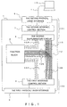
Fig.1 illustrates a PC card with reference to a first
embodiment of the present invention. In the first embodiment, a
PC card based on the PCMCIA standard is described as an example.
Fig.1 is a plan view illustrating an internal schematic structure
of the PC card 1 with a plurality of blocks.
-
As is illustrated in Fig.1, the PC card 1 has a function block
2 providing a predetermined function to the information processing
device. The function block 2 can provide one or combined functions
of a variety of functions such as a memory function, modem function
or LAN function to the information processing device. Also, the
PC card 1 has a first interface section 100 to transfer data between,
for example, a portable PC (omitted in Fig.1) and the function block
2 as a first information processing device. The omitted portable
PC in Fig.1 is assumed to have the PC card interface therein. So,
in the first embodiment, the first interface section 100 has, as
a first physical layer interface 3, a PC card physical layer
interface physically connecting to the PC card interface in the
portable PC and, as a first interface control section 4, a PC card
interface between the first physical layer interface 3 and the
function block 2.
-
The PC card 1 also has a second interface section 101 to
transfer data between a desktop PC 10 being as a second information
processing device and the function block 2. It should be noted that
the desktop PC 10 is assumed not to have the PC card interface.
Therefore, the second interface section 101 is a different
interface specification from the first interface section 100. The
second interface section 101 has a second physical layer interface
6 connected to the desktop PC 10 through a connecting cable 11,
and a second interface control section 7 arranged between the second
physical layer interface 6 and the function block 2.
-
Further, the second interface section 101 has a second
supplementary circuit 8 between the desktop PC 10 and the function
block 2 to realize a control procedure through the second interface
control section 7. The second supplementary circuit is arranged
between the function block 2 and the second interface control
section 7.
-
Now, in the PC card 1 of the first embodiment, a plurality
of signal lines 102,104,106,108 and 110 are connected from the
function block 2 to the first and second interface sections 100
and 101. At least a part of a plurality of lines from 102 to 110
diverges at the junction section 112 illustrated by dotted lines
in Fig.1 as common signal lines 106, and then connects to both of
the first signal lines 108 connecting to the first interface control
section 4 which is a PC card interface control section of the first
interface section 100 and the second signal lines 110 connecting
to the second supplementary circuit 8 of the second interface
section 101. The common signal lines 106 and the first and second
signal lines 108 and 110 in this embodiment are used as data or
address bus lines, where the data signals or address signals flow
to be transferred between the portable PC (omitted in Fig. 1) and
the function block 2 and between the desktop PC 10 and the function
block 2. Also, the signal lines 102 which connect the function block
2 to the first interface control section 4, and the signal lines
104 which connect the function block 2 to the second supplementary
circuit 8, both of them are illustrated by the dotted lines in Fig.1,
function as control signal lines to transfer the control signals
to control the function block 2 respectively.
-
Next, an operation of the PC card with reference to the
present embodiment will be described. First, the second interface
control section 7 executes an error detection and a protocol
processing and so on, for example, for serial data which are input
from the desktop PC 10 through the second physical layer interface
6, or controls to recognize the PC card 1 as a device from the side
of the desktop PC 10. At this time, to realize the control procedure
through the second interface control section 7 between the desktop
PC 10 and the function block 2, the second supplementary circuit
8 converts the data transmitted from the function block 2 to the
suitable data for the second interface control section 7, converts
data or commands, Which are transmitted from the desktop PC 10 and
executed a parallel conversion through the second physical layer
interface 6 and the second interface control section 7, in a format
understandable at the function block 2, or converts them for an
electrical interface suitable to the function block 2.
-
When the PC card 1 is used connecting to the desktop PC 10,
if the desktop PC 10 has, for example, the USB (Universal Serial
Bus) which is recently becoming a de facto standard, the data can
be transferred by using the USB interface as the second interface
control section, by providing a connector for the USB or an entry
for a connecting cable for the USB, and by connecting the PC card
1 to the desktop PC 10 with a connecting cable 11 or a wireless
communication device such as an infrared.
-
Also, when the PC card 1 is used in the portable PC, the PC
card can be used with the similar operability as the conventional
PC card by inserting 68 pins of the PC card physical layer interface
3 of the PC card 1 in the slot of the PC card drive device provided
in the Portable PC to connect.
-
It should be noted that although the first embodiment is
described by exemplifying the PC card having the PC card interface
based on the PCMCIA standard as the first interface section 100,
the above mentioned other PC card interfaces such as interfaces
used for the "compact Flash (the registered trademark of Sandisk
Corporation)", the "Small PC Card", the "Miniature Card", the
"SmartMedia (the registered trademark of Toshiba Corporation)",
"MMC (MultiMedia Card)", or the "Memory stick (the trademark of
Sony Corporation)" can be provided in the first interface section
100.
-
Also, in the first embodiment, the common signal lines 106
are diverged at the junction section 112 to connect to the first
and second interface sections 100 and 101, and therefore achieving
a reduction in change of design of the conventional existing
function block and the first interface section 100(the PC card
interface in the first embodiment) as much as possible and providing
the second interface section 101 in a compact circuit structure.
Also, if the whole PC card 1 is newly designed, signal lines directly
connected from the function block 2 to the first and second
interface sections 100 and 101 can be provided without the use of
the common signal lines 106.
-
Further, Fig.1 illustrates the structure to transfer the
data only between the function block 2 and the two information
processing devices through the first and second interface sections
100 and 101, where the function block 2 is intended to have a memory
card and the like having a memory function. When the function block
2 has functions such as a modem function or a LAN function, a
connector or mounting opening corresponding to the Modem and LAN
can be formed at a different location (for example, the left side
of the interface 6,) from the second physical layer interface 6
of the PC card 1 in Fig.1 to connect predetermined signal lines
from the function block 2 to the connector and the like. And a
variety of setting information and processing procedure are
provided from the information processing device to the PC card 1
through the first and second interface sections 100 and 101, and
then the function block 2 exercises the desired function based on
the setting information and processing procedure.
-
Further, though the above first embodiment is described
using a combination of two interfaces, the PC card interface and
the second interface section, more interfaces can be mounted in
the PC card.
-
Furthermore, in the PCMCIA standard and USB standard, the
power source voltage (Vcc) driving each circuit in the PC card 1
is supplied from the host side (the side of the information
processing device) through the interface. For example, when the
PC card 1 of the first embodiment is connected to a serial port
(such as RS232C) or an infrared communication port (such as IrDA)
which are not installed with a power source line, other external
battery can be used or a power source can be installed in the PC
card 1. Also, for example, a power source voltage can be supplied
from a connecting cable for the keyboard connector of the desktop
PC 10 to the PC card 1 by modifying the connecting cable connecting
the body of the desktop PC 10 to a keyboard, and by connecting a
specific connector for the power source outlet to the connecting
cable. In this way, for example, the PC card 1 of the first
embodiment can be used for an information processing device with
a small feeding ability such as consumer audio equipment or
information terminal equipment by supplying only a power source
from the desktop PC 10 even for the case of the PC card 1 having
a relatively large consumption power.
-
As has been previously described, since the PC card of the
first embodiment is structured to be able to correspond to a
plurality of interfaces with different specifications without
being limited to the PC card interface, the PC card can be used,
without a connection of the PC card drive device, not only for the
information processing device such as a portable PC or digital
camera having a connector for the PC card but also for the
information processing device which does not include a PC card
interface as a standard such as a desktop PC, therefore increasing
a portability and flexibility the PC card originally owns.
Second Embodiment
-
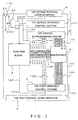
Next, a PC card of the present invention will be described
with reference to the second embodiment in Fig.2. The second
embodiment is described by exemplifying a PC card based on the
standard of the PCMCIA similar to the first embodiment. Fig.2 is
a plan view illustrating an internal schematic structure of a PC
card 20 with a plurality of blocks. The same code is designated
to the structure element which has the same functional operation
as the structure element of the PC card 1 of the first embodiment
in Fig.1 to omit detailed descriptions.
-
The PC card 20 of the second embodiment provides a signal
switching section as a means of switching to select one of the first
and second interface sections 100 and 101 to connect the selected
one to the function block 2. The signal switching section has a
multiplexer 21 to electrically connect the common signal lines 106
to one of the first signal lines 108 and the second signal lines
110. The multiplexer 21 is arranged at the junction section 112
on the signal lines in Fig.1. Also, the signal switching section
has a multiplexer control circuit comprising a switch 23 and a bus
selector control logic 24 structured with an integrated circuit.
The switch 23 and the bus selector control logic 24 are positioned
on the left side of the second physical layer interface 6 in Fig.2.
One of the two terminals of the switch 23 is grounded (ground
potential) and the other is connected to an input terminal of the
bus selector control logic 24. Both terminals of the switch 23
come to a closed state (ON) with a connection between the terminals
by pushing a switching button 118 projecting out of the body of
equipment of the PC card 20, and both terminals of the switch 23
come to an open state (OFF) with disconnection between them by
pulling up the switching button 118.
-
An arrangement of the power source lines in the PC card will
be described here. The power source line 120 is connected to a pin
terminal among the 68 pin terminals of the first physical layer
interface 3 which is a PC card physical layer interface, where a
power source voltage Vcc1 is supplied to the pin terminal. The
power source line 120 supplies a power to the function block 2 by
being connected to the function block 2 and is also connected to
other input terminal of the bus selector control logic 24. On the
other hand, a power source voltage Vcc2 from the second physical
layer interface 6 is supplied to the power source line 124, and
the power source line 124 supplies the power to the function block
by being connected to the function block 2 as well as the power
source line 124 is connected to other input terminal of the bus
selector control logic 24.
-
Also, an output line of the bus selector control logic 24
is connected to the bus switch enable pin BX of the multiplexer
with a signal line 126.
-
Based on the first power source voltage Vcc1 supplied from
the portable PC omitted in Fig.2 to the first interface section
100 and the second power source voltage Vcc2 supplied from the
desktop PC to the second interface section 101, the signal switching
section having a arrangement structure as described above forms
a state of electrically non-connection by maintaining one of the
first signal lines 108 and the second signal lines 110 relatively
in a high impedance state to the common signal lines 106 , and
operates to connect the other signal lines to the common signal
lines 106. Further, the switch 23 of the signal line switching
section is used to select one of the first signal line 108 and the
second signal line 110 when both of the first power source voltage
Vcc1 and the second power source voltage Vcc2 are supplied. They
will be later described in detail.
-
Next, the operation of the PC card 20 will be described with
reference to the second embodiment. It should be noted that the
information processing devices are connected to the first and
second interface section 100 and 101 respectively. In short, the
first physical layer interface 3 is inserted in the slot of the
PC card drive device, for example the PC card slot installed in
the notebook PC or the PC card drive device of the external type,
in the portable PC omitted in Fig. 2, and the second physical layer
interface 6 is connected, as illustrated in Fig.1, to the UBS
connector in the desktop PC through the connecting cable 11. In
such a case, it is required to select which information processing
device is used with the PC card 20 for a data transfer. It is also
required that the data transfer is not affected by the other
interface section when the date is under transfer at one interface
section.
-
Therefore, when the second interface control section 7 and
the second supplementary control circuit 8 are not used, the second
signal lines 110 connected to the second supplementary circuit 8
must be maintained in a high impedance state to the first interface
control section 4. Or, on the contrary, when the first interface
control section 4 is not used, the first signal lines 108 connected
to the first interface control section 4 must be maintained in a
high impedance state to the second supplementary circuit 8.
-
When a High (H) voltage is applied to a bus switch enable
pin BX of the
multiplexer 21, in short when a signal "1" is output
from the bus
selector control logic 24, the
multipexer 21 of the
first embodiment sets the side of the
second signal lines 110 in
a high impedance state, and thereby connecting the
common signal
lines 106 from the
function block 2 to the
first signal lines 108
on the side of the first
interface control section 4. Also, when
a Low (L) voltage is applied to the bus switch enable pin BX, in
short when a signal "0" is output from the bus
selector control
logic 24, the
multiplexer 21 sets the side of the
first signal lines
108 in a high impedance state, and thereby connecting the
common
signal lines 106 to the
second signal line 110 on the side of the
second
supplementary circuit 8. Table 1 illustrates a table of
true value showing the operation of the bus
selector control logic
24.
-
In table 1, (1) indicates the first interface section 100,
where (2) indicates the second interface section 101. "SW"
indicates a level of the switching signal inputting in the bus
selector control logic 24, where "L" indicates a low state due to
a ground voltage applied by closing(ON) the switch 23, and "Hiz"
indicates a high state(a high impedance state) due to the open state
of the switch 23. As is clear from the table of true value, when
the power source voltage Vcc1 is input from the portable PC and
the power source voltage Vcc2 is input from the USB connector of
the desktop PC or from aforementioned keyboard connecting cable,
the signal "0" is output at an output terminal (OUT) by closing
(ON) the switch 23 to set the input (SW) of the bus selector control
logic 24 in a low state (L), and a signal "1" is output at the output
terminal (OUT) by opening the switch 23 to set the input(SW) of
the bus selector control logic 24 in the high state(HiZ).
-
Whether the switch is in high state or in low state, when
Vcc1 is applied and Vcc2 is not applied, the signal "1" is output
from the output terminal (OUT) of the bus selector control logic
24. On the other hand, When Vcc2 is applied and Vcc1 is not applied,
the signal "0" is output.
-
Thus, in the open state of the switch 23 as illustrated in
Fig.2, when the side of the first physical layer interface 3 of
the PC card 20 is inserted in the slot of the PC card drive device
of the portable PC and when the second physical layer interface
6 is connected to the USB connector of the desktop PC 10 by the
connecting cable 11 in Fig. 1, the power source voltage Vcc2 is input
from the desktop PC 10 to the bus selector control logic 24 through
the second physical layer interface 6. Since the switch 23 is in
the open state, input (SW) at the bus selector control logic 24
is in a high state (HiZ), therefore outputting a signal "1" at the
output terminal (OUT) to input it in the bus switch enable pin BX
of the multiplexer 21. The multiplexer 21 sets the side of the second
supplementary circuit 8 in the state of high impedance to switch
the connection of the common signal lines 106 from the function
block 2 to the side of the first interface control section 4. In
this way, for example, even if the PC card 20 is connected to both
of the portable PC and desktop PC, only the data transmission from
the portable PC to the PC card 20 is executed, but the access from
the desktop PC to the PC card 20 is not executed.
-
To make it possible for the desktop PC to access to the PC
card 20 from this state, the switch 23 is switched to closed state
(ON). In this way, the input (SW) of the bus selector control logic
24 is set in the low state (L) to output a signal "0" at the output
terminal (OUT), then inputting the signal to the bus switch enable
pin BX of the multiplexer 21. The multiplexer 21 sets the side
of the first interface control section 4 in the high impedance state
to switch the connection of the common signal lines 106 from the
function block 2 to the side of the second supplementary circuit
8. Thus, the PC card 20 is set in a connecting state to the desktop
PC connected to the second physical layer interface 6, so that the
access from the portable PC to the PC card 20 is not possible. It
should be noted that no problem is introduced when the interface
does not have a dynamic setting means by plug & pay because a
recognition can be made by resetting from the software operating
in the information processing device.
Third Embodiment
-
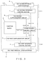
Next, A PC card of the present invention will be described
with reference to the third embodiment in Fig.3. The third
embodiment is also described by exemplifying the PC card based on
the PCMCIA standard similar to the first and second embodiments.
Fig.3 is a plan view illustrating an internal schematic structure
of the PC card 30 with a plurality of blocks. The same code is
designated to the structure element having the same functional
operation as the structure element in the PC cards 1 and 20 in the
first and second embodiments illustrated in Fig.1 and Fig. 2 to omit
detailed descriptions. The illustration of the common signal
lines from the function block 2 and the signal lines (including
the control signal lines) connected to the first and interface
sections 100 and 101 is omitted in Fig.3.
-
The PC card 30 of the third embodiment provides a power source
control circuit 31 as a switching means to select one of the first
and second interface section 100 and 101 and to connect the selected
one to the function block 2. The power source control circuit 31
controls a voltage Vcc1-in and a voltage Vcc2-in supplied to the
first interface section 100 and the second interface section 101
to operate to deactivate one of the first and second interface
sections 100 and 101. Also, the first interface section 100 of the
PC card 30 of the third embodiment has the first supplementary
circuit 5 between the first interface control section 4 and the
function block 2.
-
The illustrated voltage "Vcc1-in" in Fig.3 shows that the
power source voltage Vcc1 from the first interface control section
4 inputs in the power source control circuit 31. Notation "in"
and "out" show an input and output of the power source control
circuit 31. For example, "Vcc1-in" shows that a power source
voltage Vcc1 inputs in the power source control circuit 31 and the
"Vcc1-out" shows that the power source voltage Vcc1 is output from
the power source control circuit 31.
-
The power source control circuit 31 of the third embodiment
outputs the voltage Vcc1 and voltage VccF when the power source
voltage Vcc1 is input and the voltage Vcc2 and voltage VccF when
the power source voltage Vcc2 is input. When both of the power source
voltages Vcc1 and Vcc2 are input, the power source control circuit
31 is structured to output the Vcc1 and VccF. It should be noted
that the VccF is a voltage supplied to the function block 2.
-
When the PC card 30 is inserted in the slot of the PC card
drive device in the portable PC, the power source voltage Vcc1 is
input from the first interface control section 4 to the power source
control circuit 31. In this way, the power source voltage Vcc1 is
output from the power source control circuit 31 to the first
supplementary circuit 5, and the power source voltage VccF is output
to the function block 2. Thus, the function block 2 and the first
supplementary circuit 5 are set in the deactivate state, so that
an access from the portable PC to the PC card 30 can be executed.
-
Also, when the PC card 30 is not inserted in the slot of the
PC card drive device of the portable PC and the second physical
layer interface 6 is connected to the USB connector of the desktop
PC, the power source voltage Vcc2 is input from the second interface
control section 7 to the power source control circuit 31.
Therefore, the power source voltage Vcc2 is output from the power
source control circuit 31 to the second supplementary circuit 8,
while the power source voltage VccF is output to the function block
2. Thus, the function block 2 and the second supplementary circuit
8 are activated to access from the desktop PC to the PC card 30.
-
When the PC card 30 is inserted in the slot of PC card drive
device of the portable PC and the second physical layer interface
6 is connected to the USB connector in the desktop PC, the power
source voltage Vcc1 is input from the first interface control
section 4 to the power source control circuit 31, and also the power
source voltage Vcc2 is input from the second interface control
section 7. At this time, as has been previously described, the
power source control circuit 31 outputs the power source voltage
Vcc1 to the first supplementary circuit 5 and the power source
voltage VccF to the function block 2, so that the function block
2 and the first supplementary circuit 5 are activated and the second
interface section 101 is deactivated.
-
Thus, in the third embodiment, when the data is transferred
between the function block 2 and the first or second interface
section 100 or 101, the power source control circuit 31 is provided
to supply the power only to the side of the interface section which
transfers the data and to the function block 2 without a supply
of the power to the side of the interface which should be in the
deactivated state not to transfer the data, and therefore the data
to be transferred can be easily and surely transferred as well as
the switching of the activation or deactivation of the interface
can be executed by a simpler structure than a complex multiplexer
in structure.
-
Further, in the third embodiment, when the information
processing devices are connected to the first and second interface
sections 100 and 101, it is decided that the right to access is
given to the information processing device connected to the first
interface section 100. However, without being limited to this, for
example, the PC card 30 can be structured to allow the information
processing device connected earlier to have the priority to access
to it, or the user can transfer the data alternatively to the
portable PC and desktop PC by connecting arbitrarily even if the
PC card 30 is connected to both of the portable PC and desktop PC
by providing a switch circuit such as one illustrated in the second
embodiment.
Fourth Embodiment
-
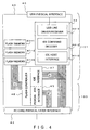
Next, a PC card of the present invention will be described
with reference to the fourth embodiment in Fig.4. In the fourth
embodiment, the PCMCIA ATA (AT Attachment) card recently widely
used as a storage media of the digital-still-camera and portable
terminal is described as an example. Fig.4 is a plan view
illustrating an internal schematic structure of a PC 40 with a
plurality of blocks.
-
Fig.4 illustrates that the first interface section 100 has
a PCMCIA ATA interface 45 together with a PC card physical layer
interface 42 while the second interface section 101 has a USB
physical layer interface 43, a USB interface 44, and an IDE
(Integrated Drive Electronics) interface 47. These first and
second interface sections 100 and 101 are connected to a flash
controller 46.
-
Among a plurality of signal lines A and B connected from the
PCMCIA ATA interface 45 to the PC card physical layer interface
42, the common signal lines A which are the data or address lines
are connected also to the USB interface 44 after divergence. The
desktop PC can be accessed to the PC card (the PCMCIA ATA Card)
40 by being connected from the USB interface 44 to the USB port
of the desktop PC through the USB physical layer interface 43 and
the connecting cable.
-
As is illustrated in Fig.4, the PC card 40 provides flash
memories 41-1, 41-2, and 41-3. These flash memories 41-1, 41-2,
and 41-3 are connected to the flash controller 46 arranged between
the flash memory 41-3, the PCMCIA ATA interface 45 and the IDE
interface 47 by control signal lines C.
-
Further, a USB line driver/receiver 44-1, an IDE command
decoder 44-2, and an IDE host interface 44-3 are provided in the
USB interface 44.
-
A driver/receiver is provided in the PCMCIA ATA interface
45 to connect the common signal lines A and the non-common signal
lines B to the PC card physical layer interface 42, where the common
signal lines A share the lines with the IDE interface 44-3 but the
non-common signal lines B do not share the lines with the IDE
interface 44-3.
-
The flash controller 46 operates as a PC card interface and
decodes input signals input to the common signal lines A and
non-common signal lines B. Also, based on the decoded input signal,
the flash controller 46 executes the processing to the flash memory
41-1∼41-3 through control signal lines C, or executes a processing
to the flash memory 41-1∼41-3 with a control signal transmitted
through the common signal lines A based on a result decoded by the
IDE command decoder 44-2.
-
Signal lines of the
USB interface 44 will be described with
reference to Table 2. As is illustrated in Table 2, the signal lines
of the
USB interface 44 provide a power source voltage Vcc=5V,
differential data signal lines D+ and D-, and a grounding line.
It should be noted that the USB
physical layer interface 43 in the
PC card 40 has two connection ports for serial connections with
other peripheral devises.
-
The control signals are transmitted through the PC card
physical layer interface 42 when the PC card 40 is inserted in the
slot of the PC card driving device in the portable PC. Among the
control signals, the control signals shared with the IDE host
interface 44-3 are transmitted to the common signal lines A, where
unshared control signals are transmitted to the non-common signal
lines B. The control signals transmitted to the common signal lines
A and non-common signal lines B are decoded at the flash controller
46 through the PCMCIA ATA interface 45, and a processing
corresponding to the decoded control signals is executed at the
flash memories 41-1∼41-3. Data resulted from the processing at the
flash memories 41-1∼41-3 are transmitted from the flash controller
46 to the PCMCIA ATA interface 45, and then transmitted to the
portable PC through the PC card physical layer interface 42. In
this way, the PC card 40 can be operated as the PCMCIA ATA card.
-
On the other hand, when the connector of the USB connecting
cable connected to the USB port in the desktop PC and the USB
physical layer interface 43 of the PC card 40 are connected, the
control signals (serial signals) from the desktop PC are received
at the receiver of the USB line driver/receiver 44-1 after they
are input, and then a serial/parallel conversion of the control
signals is executed.
-
After the control signals converted to the parallel signals
are decoded at the IDE command decoder 44-2, they are output to
the common signal lines A through the IDE host interface 44-3. The
control signals output to the common signal lines A are transmitted
to the flash controller 46 through the IDE interface 47, and then
a predetermined processing is executed to the flash memories
41-1∼41-3. From the operation described above, the PC card 40 can
be operated as the IDE drive connected to the USB port in the desktop
PC.
-
Also, in the PC card of the fourth embodiment, the connection
with the information processing device can be executed by the
wireless connection such as an infrared transmission, or by
receiving the power source lines from the connecting cable of the
desktop PC.
-
Furthermore, in the PC card of the above first through fourth
embodiments, the second interface section 101 is described as being
corresponding to the USB standard. However, for example, the second
interface section 101 of the PC card 1,20,30,and 40 of the above
embodiments can be an interface corresponding to the IEEE1394
standard as long as the desktop PC has a interface and connector
corresponding to the IEEE1394 standard.
-
As has been previously described, the present invention can
realize a PC card connectable to a plurality of information
processing devices without losing the advantages of easy
detachability, flexibility and portability of the PC card
originally owned by the PC card. The present invention can also
realize a PC card connectable to the information processing devices
which do not have a PC card drive device. Further, the present
invention can realize a PC card connectable to an interface
pre-provided in the information processing devices as a standard.