EP0932929B1 - Active rectifier circuit - Google Patents
Active rectifier circuit Download PDFInfo
- Publication number
- EP0932929B1 EP0932929B1 EP97944921A EP97944921A EP0932929B1 EP 0932929 B1 EP0932929 B1 EP 0932929B1 EP 97944921 A EP97944921 A EP 97944921A EP 97944921 A EP97944921 A EP 97944921A EP 0932929 B1 EP0932929 B1 EP 0932929B1
- Authority
- EP
- European Patent Office
- Prior art keywords
- power source
- switching transistor
- transistors
- mosfet
- winding
- Prior art date
- Legal status (The legal status is an assumption and is not a legal conclusion. Google has not performed a legal analysis and makes no representation as to the accuracy of the status listed.)
- Expired - Lifetime
Links
Images


Classifications
-
- H—ELECTRICITY
- H02—GENERATION; CONVERSION OR DISTRIBUTION OF ELECTRIC POWER
- H02M—APPARATUS FOR CONVERSION BETWEEN AC AND AC, BETWEEN AC AND DC, OR BETWEEN DC AND DC, AND FOR USE WITH MAINS OR SIMILAR POWER SUPPLY SYSTEMS; CONVERSION OF DC OR AC INPUT POWER INTO SURGE OUTPUT POWER; CONTROL OR REGULATION THEREOF
- H02M3/00—Conversion of dc power input into dc power output
- H02M3/22—Conversion of dc power input into dc power output with intermediate conversion into ac
- H02M3/24—Conversion of dc power input into dc power output with intermediate conversion into ac by static converters
- H02M3/28—Conversion of dc power input into dc power output with intermediate conversion into ac by static converters using discharge tubes with control electrode or semiconductor devices with control electrode to produce the intermediate ac
- H02M3/325—Conversion of dc power input into dc power output with intermediate conversion into ac by static converters using discharge tubes with control electrode or semiconductor devices with control electrode to produce the intermediate ac using devices of a triode or a transistor type requiring continuous application of a control signal
- H02M3/335—Conversion of dc power input into dc power output with intermediate conversion into ac by static converters using discharge tubes with control electrode or semiconductor devices with control electrode to produce the intermediate ac using devices of a triode or a transistor type requiring continuous application of a control signal using semiconductor devices only
- H02M3/33569—Conversion of dc power input into dc power output with intermediate conversion into ac by static converters using discharge tubes with control electrode or semiconductor devices with control electrode to produce the intermediate ac using devices of a triode or a transistor type requiring continuous application of a control signal using semiconductor devices only having several active switching elements
- H02M3/33576—Conversion of dc power input into dc power output with intermediate conversion into ac by static converters using discharge tubes with control electrode or semiconductor devices with control electrode to produce the intermediate ac using devices of a triode or a transistor type requiring continuous application of a control signal using semiconductor devices only having several active switching elements having at least one active switching element at the secondary side of an isolation transformer
- H02M3/33592—Conversion of dc power input into dc power output with intermediate conversion into ac by static converters using discharge tubes with control electrode or semiconductor devices with control electrode to produce the intermediate ac using devices of a triode or a transistor type requiring continuous application of a control signal using semiconductor devices only having several active switching elements having at least one active switching element at the secondary side of an isolation transformer having a synchronous rectifier circuit or a synchronous freewheeling circuit at the secondary side of an isolation transformer
-
- Y—GENERAL TAGGING OF NEW TECHNOLOGICAL DEVELOPMENTS; GENERAL TAGGING OF CROSS-SECTIONAL TECHNOLOGIES SPANNING OVER SEVERAL SECTIONS OF THE IPC; TECHNICAL SUBJECTS COVERED BY FORMER USPC CROSS-REFERENCE ART COLLECTIONS [XRACs] AND DIGESTS
- Y02—TECHNOLOGIES OR APPLICATIONS FOR MITIGATION OR ADAPTATION AGAINST CLIMATE CHANGE
- Y02B—CLIMATE CHANGE MITIGATION TECHNOLOGIES RELATED TO BUILDINGS, e.g. HOUSING, HOUSE APPLIANCES OR RELATED END-USER APPLICATIONS
- Y02B70/00—Technologies for an efficient end-user side electric power management and consumption
- Y02B70/10—Technologies improving the efficiency by using switched-mode power supplies [SMPS], i.e. efficient power electronics conversion e.g. power factor correction or reduction of losses in power supplies or efficient standby modes
Landscapes
- Engineering & Computer Science (AREA)
- Power Engineering (AREA)
- Rectifiers (AREA)
- Control Of Motors That Do Not Use Commutators (AREA)
- Control Of Eletrric Generators (AREA)
- Dc-Dc Converters (AREA)
- Electronic Switches (AREA)
- Amplifiers (AREA)
- Mechanical Treatment Of Semiconductor (AREA)
- Electrical Discharge Machining, Electrochemical Machining, And Combined Machining (AREA)
- Power Conversion In General (AREA)
- Semiconductor Integrated Circuits (AREA)
- Emergency Protection Circuit Devices (AREA)
Abstract
Description
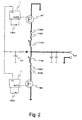
- a first control transformer and a second control transformer, whereby
- a first winding of said first control transformer is connected in between the drain of said first switching transistor and the other end of said first secondary winding,
- a first winding of said second control transformer is connected in between the drain of said second switching transistor and the other end of said second secondary winding;
- a second winding of said first control transformer is connected to the first switching transistor control circuit, and
- a second winding of said second control transformer is connected to the second switching transistor control circuit;
- a third winding of said first control transformer is connected between the other end of said second secondary winding and the drain of said second switching transistor, and
- a third winding of said second control transformer is connected between the other end of said first secondary winding and the drain of said first switching transistor.
- figure 1
- illustrates a MOSFET rectifier circuit according to the prior art,
- figure 2
- illustrates a preferred embodiment according to the invention,
- figure 3
- illustrates another preferred embodiment according to the invention,
- figure 4
- illustrates a gate control circuit of a MOSFET, suited for the system of figure 2, and
- figure 5
- illustrates a third preferred embodiment according to the invention.
Claims (4)
- A power source comprising a mains transformer (T1), said mains transformer including a first (T1N2) and second (T1N3) secondary winding, and the power source further comprising two switching transistors (M1,M2) for rectifying the current of said secondary windings, and in which power sourceand which power source further hasthe sources of said switching transistors are connected to fixed potential,the first end of said first secondary winding (T1N2) is connected to the first outlet of the power source,the source of the first switching transistor (M1) is connected to the second outlet of the power source, andin between the other end of said first secondary winding and the drain of the first switching transistor, there is connected at least a wire; and thatthe first end of said second secondary winding (T1N3) is connected to the first outlet of the power source,the source of the second switching transistor (M2) is connected to the second outlet of the power source, andin between the other end of said secondary winding and the drain of the second switching transistor, there is connected at least a wire;characterised in thata first switching transistor control circuit (1) which is connected to the gate of the first switching transistor,a second switching transistor control circuit (1) which is connected to the gate of the second switching transistor,
the power source further comprisesa first control transformer (T3) and a second control transformer (T4), wherebya first winding (T3N1) of said first control transformer (T3) is connected in between the drain of said first switching transistor (M1) and the other end of said first secondary winding (T1N2),a first winding (T4N2) of said second control transformer is connected in between the drain of said second switching transistor (M2) and the other end of said second secondary winding (T1N3);a second winding (T3N3) of said first control transformer (T3) is connected to the first switching transistor control circuit (1), anda second winding (T4N3) of said second control transformer (T4) is connected to the second switching transistor control circuit (1);a third winding (T3N2) of said first control transformer is connected between the other end of said second secondary winding (T1N3) and the drain of said second switching transistor (M2), anda third winding (T4N1) of said second control transformer (T4) is connected between the other end of said first secondary winding (T1N2) and the drain of said first switching transistor (M1). - The power source of claim 1, characterised in that said first outlet of the power source is the positive outlet of the power source, that said second outlet of the power source is the outlet of the ground potential of the power source and that said switching transistors (M1,M2) are n-type switching transistors (M1,M2).
- The power source of claim 1, characterised in that said first outlet of the power source is the negative outlet of the power source, that said second outlet of the power source is the outlet of the ground potential of the power source and that said switching transistors (M1,M2) are p-type switching transistors (M1,M2).
- The power source of claim 1, characterised in that said switching transistor (M1,M2) is a MOSFET.
Applications Claiming Priority (3)
| Application Number | Priority Date | Filing Date | Title |
|---|---|---|---|
| FI964184A FI114056B (en) | 1996-10-18 | 1996-10-18 | Power source |
| FI964184 | 1996-10-18 | ||
| PCT/FI1997/000632 WO1998018198A1 (en) | 1996-10-18 | 1997-10-17 | Active rectifier circuit |
Publications (2)
| Publication Number | Publication Date |
|---|---|
| EP0932929A1 EP0932929A1 (en) | 1999-08-04 |
| EP0932929B1 true EP0932929B1 (en) | 2002-08-14 |
Family
ID=8546900
Family Applications (1)
| Application Number | Title | Priority Date | Filing Date |
|---|---|---|---|
| EP97944921A Expired - Lifetime EP0932929B1 (en) | 1996-10-18 | 1997-10-17 | Active rectifier circuit |
Country Status (10)
| Country | Link |
|---|---|
| EP (1) | EP0932929B1 (en) |
| AT (1) | ATE222424T1 (en) |
| DE (1) | DE69714753T2 (en) |
| DK (1) | DK0932929T3 (en) |
| ES (1) | ES2181032T3 (en) |
| FI (1) | FI114056B (en) |
| NO (1) | NO991848L (en) |
| PL (1) | PL184963B1 (en) |
| RU (1) | RU2190293C2 (en) |
| WO (1) | WO1998018198A1 (en) |
Cited By (2)
| Publication number | Priority date | Publication date | Assignee | Title |
|---|---|---|---|---|
| US8023290B2 (en) | 1997-01-24 | 2011-09-20 | Synqor, Inc. | High efficiency power converter |
| US10199950B1 (en) | 2013-07-02 | 2019-02-05 | Vlt, Inc. | Power distribution architecture with series-connected bus converter |
Families Citing this family (2)
| Publication number | Priority date | Publication date | Assignee | Title |
|---|---|---|---|---|
| WO2001055142A1 (en) * | 2000-01-28 | 2001-08-02 | Syngenta Limited | Isothiazole derivatives and their use as pesticides |
| GB2370431A (en) * | 2000-12-19 | 2002-06-26 | Brian Victor Olliver | A dc-ac-dc power converter |
Family Cites Families (2)
| Publication number | Priority date | Publication date | Assignee | Title |
|---|---|---|---|---|
| DE3422777A1 (en) * | 1984-06-20 | 1986-01-02 | ANT Nachrichtentechnik GmbH, 7150 Backnang | Controlled rectifier element, which is connected to an inductor, and its use |
| US5179512A (en) * | 1991-09-18 | 1993-01-12 | General Electric Company | Gate drive for synchronous rectifiers in resonant converters |
-
1996
- 1996-10-18 FI FI964184A patent/FI114056B/en active
-
1997
- 1997-10-17 EP EP97944921A patent/EP0932929B1/en not_active Expired - Lifetime
- 1997-10-17 RU RU99109589/09A patent/RU2190293C2/en not_active IP Right Cessation
- 1997-10-17 AT AT97944921T patent/ATE222424T1/en not_active IP Right Cessation
- 1997-10-17 DE DE69714753T patent/DE69714753T2/en not_active Expired - Lifetime
- 1997-10-17 DK DK97944921T patent/DK0932929T3/en active
- 1997-10-17 WO PCT/FI1997/000632 patent/WO1998018198A1/en active IP Right Grant
- 1997-10-17 ES ES97944921T patent/ES2181032T3/en not_active Expired - Lifetime
- 1997-10-17 PL PL97332824A patent/PL184963B1/en not_active IP Right Cessation
-
1999
- 1999-04-16 NO NO991848A patent/NO991848L/en not_active Application Discontinuation
Cited By (7)
| Publication number | Priority date | Publication date | Assignee | Title |
|---|---|---|---|---|
| US8023290B2 (en) | 1997-01-24 | 2011-09-20 | Synqor, Inc. | High efficiency power converter |
| US8493751B2 (en) | 1997-01-24 | 2013-07-23 | Synqor, Inc. | High efficiency power converter |
| US9143042B2 (en) | 1997-01-24 | 2015-09-22 | Synqor, Inc. | High efficiency power converter |
| US10199950B1 (en) | 2013-07-02 | 2019-02-05 | Vlt, Inc. | Power distribution architecture with series-connected bus converter |
| US10594223B1 (en) | 2013-07-02 | 2020-03-17 | Vlt, Inc. | Power distribution architecture with series-connected bus converter |
| US11075583B1 (en) | 2013-07-02 | 2021-07-27 | Vicor Corporation | Power distribution architecture with series-connected bus converter |
| US11705820B2 (en) | 2013-07-02 | 2023-07-18 | Vicor Corporation | Power distribution architecture with series-connected bus converter |
Also Published As
| Publication number | Publication date |
|---|---|
| NO316852B1 (en) | 1999-04-16 |
| NO991848D0 (en) | 1999-04-16 |
| FI964184A0 (en) | 1996-10-18 |
| FI114056B (en) | 2004-07-30 |
| PL332824A1 (en) | 1999-10-11 |
| ATE222424T1 (en) | 2002-08-15 |
| NO991848L (en) | 1999-04-16 |
| DK0932929T3 (en) | 2002-12-16 |
| DE69714753D1 (en) | 2002-09-19 |
| FI964184A (en) | 1998-04-19 |
| ES2181032T3 (en) | 2003-02-16 |
| DE69714753T2 (en) | 2003-04-30 |
| WO1998018198A1 (en) | 1998-04-30 |
| RU2190293C2 (en) | 2002-09-27 |
| PL184963B1 (en) | 2003-01-31 |
| EP0932929A1 (en) | 1999-08-04 |
Similar Documents
| Publication | Publication Date | Title |
|---|---|---|
| KR100852550B1 (en) | A method and circuit for self-driven synchronous rectification | |
| US6256214B1 (en) | General self-driven synchronous rectification scheme for synchronous rectifiers having a floating gate | |
| US5471376A (en) | Low-loss active voltage-clamp circuit for single-ended forward PWM converter | |
| US9293999B1 (en) | Automatic enhanced self-driven synchronous rectification for power converters | |
| US5303138A (en) | Low loss synchronous rectifier for application to clamped-mode power converters | |
| US7564704B2 (en) | Method of forming a power supply controller and structure therefor | |
| US20140126247A1 (en) | Snubber circuit for dc-dc voltage converter | |
| US11742758B2 (en) | Boost converter and control method | |
| KR20060055415A (en) | Three level dc-dc converter using zero voltage and zero current switching | |
| US6477064B1 (en) | High efficiency DC-DC power converter with turn-off snubber | |
| US5920473A (en) | Dc-to-Dc power converter with integrated magnetic power transformer | |
| US6856520B2 (en) | Double sided IGBT phase leg architecture and clocking method for reduced turn on loss | |
| Toba et al. | Auxiliary resonant commutated pole inverter using two internal voltage-points of DC source | |
| EP0932929B1 (en) | Active rectifier circuit | |
| Voss et al. | Adapted auxiliary-resonant commutated pole in the dual-active bridge | |
| EP0942520A2 (en) | DC to DC power converter | |
| Kayser et al. | Hybrid Switch with SiC MOSFET and fast IGBT for High Power Applications | |
| JP3321203B2 (en) | Isolated switching circuit, isolated switching circuit with shield function, and isolated switching circuit | |
| JPH07337022A (en) | Power converter employing auxiliary resonance commutation circuit | |
| Ziemba et al. | Efficient IGBT switching | |
| JP4717621B2 (en) | Power circuit | |
| CN113824320A (en) | Boost converter with passive lossless buffer | |
| JPH0223112Y2 (en) | ||
| JPH0683043B2 (en) | Switching circuit | |
| Patni et al. | Optimised power stages for high frequency 380/440 VAC medium power switch mode supplies |
Legal Events
| Date | Code | Title | Description |
|---|---|---|---|
| PUAI | Public reference made under article 153(3) epc to a published international application that has entered the european phase |
Free format text: ORIGINAL CODE: 0009012 |
|
| 17P | Request for examination filed |
Effective date: 19990423 |
|
| AK | Designated contracting states |
Kind code of ref document: A1 Designated state(s): AT BE CH DE DK ES FR GB IT LI NL SE |
|
| 17Q | First examination report despatched |
Effective date: 20000127 |
|
| GRAG | Despatch of communication of intention to grant |
Free format text: ORIGINAL CODE: EPIDOS AGRA |
|
| RAP1 | Party data changed (applicant data changed or rights of an application transferred) |
Owner name: OY LEXEL FINLAND AB |
|
| GRAG | Despatch of communication of intention to grant |
Free format text: ORIGINAL CODE: EPIDOS AGRA |
|
| GRAG | Despatch of communication of intention to grant |
Free format text: ORIGINAL CODE: EPIDOS AGRA |
|
| GRAH | Despatch of communication of intention to grant a patent |
Free format text: ORIGINAL CODE: EPIDOS IGRA |
|
| GRAH | Despatch of communication of intention to grant a patent |
Free format text: ORIGINAL CODE: EPIDOS IGRA |
|
| GRAA | (expected) grant |
Free format text: ORIGINAL CODE: 0009210 |
|
| AK | Designated contracting states |
Kind code of ref document: B1 Designated state(s): AT BE CH DE DK ES FR GB IT LI NL SE |
|
| REF | Corresponds to: |
Ref document number: 222424 Country of ref document: AT Date of ref document: 20020815 Kind code of ref document: T |
|
| REG | Reference to a national code |
Ref country code: GB Ref legal event code: FG4D |
|
| REG | Reference to a national code |
Ref country code: CH Ref legal event code: EP |
|
| REG | Reference to a national code |
Ref country code: CH Ref legal event code: NV Representative=s name: E. BLUM & CO. PATENTANWAELTE |
|
| REF | Corresponds to: |
Ref document number: 69714753 Country of ref document: DE Date of ref document: 20020919 |
|
| REG | Reference to a national code |
Ref country code: DK Ref legal event code: T3 |
|
| ET | Fr: translation filed | ||
| REG | Reference to a national code |
Ref country code: ES Ref legal event code: FG2A Ref document number: 2181032 Country of ref document: ES Kind code of ref document: T3 |
|
| PLBE | No opposition filed within time limit |
Free format text: ORIGINAL CODE: 0009261 |
|
| STAA | Information on the status of an ep patent application or granted ep patent |
Free format text: STATUS: NO OPPOSITION FILED WITHIN TIME LIMIT |
|
| 26N | No opposition filed |
Effective date: 20030515 |
|
| REG | Reference to a national code |
Ref country code: CH Ref legal event code: PFA Owner name: OY LEXEL FINLAND AB Free format text: OY LEXEL FINLAND AB#OLARINLUOMA 14#02200 ESPOO (FI) -TRANSFER TO- OY LEXEL FINLAND AB#OLARINLUOMA 14#02200 ESPOO (FI) |
|
| PGFP | Annual fee paid to national office [announced via postgrant information from national office to epo] |
Ref country code: SE Payment date: 20091026 Year of fee payment: 13 Ref country code: ES Payment date: 20091022 Year of fee payment: 13 Ref country code: DK Payment date: 20091027 Year of fee payment: 13 Ref country code: DE Payment date: 20091027 Year of fee payment: 13 Ref country code: CH Payment date: 20091014 Year of fee payment: 13 Ref country code: AT Payment date: 20091027 Year of fee payment: 13 |
|
| PGFP | Annual fee paid to national office [announced via postgrant information from national office to epo] |
Ref country code: NL Payment date: 20091029 Year of fee payment: 13 |
|
| PGFP | Annual fee paid to national office [announced via postgrant information from national office to epo] |
Ref country code: IT Payment date: 20091022 Year of fee payment: 13 Ref country code: GB Payment date: 20091027 Year of fee payment: 13 Ref country code: FR Payment date: 20091110 Year of fee payment: 13 |
|
| PGFP | Annual fee paid to national office [announced via postgrant information from national office to epo] |
Ref country code: BE Payment date: 20091023 Year of fee payment: 13 |
|
| BERE | Be: lapsed |
Owner name: OY *LEXEL FINLAND A.B. Effective date: 20101031 |
|
| REG | Reference to a national code |
Ref country code: NL Ref legal event code: V1 Effective date: 20110501 |
|
| REG | Reference to a national code |
Ref country code: DK Ref legal event code: EBP |
|
| REG | Reference to a national code |
Ref country code: CH Ref legal event code: PL |
|
| GBPC | Gb: european patent ceased through non-payment of renewal fee |
Effective date: 20101017 |
|
| PG25 | Lapsed in a contracting state [announced via postgrant information from national office to epo] |
Ref country code: CH Free format text: LAPSE BECAUSE OF NON-PAYMENT OF DUE FEES Effective date: 20101031 Ref country code: FR Free format text: LAPSE BECAUSE OF NON-PAYMENT OF DUE FEES Effective date: 20101102 Ref country code: LI Free format text: LAPSE BECAUSE OF NON-PAYMENT OF DUE FEES Effective date: 20101031 |
|
| REG | Reference to a national code |
Ref country code: FR Ref legal event code: ST Effective date: 20110630 |
|
| PG25 | Lapsed in a contracting state [announced via postgrant information from national office to epo] |
Ref country code: BE Free format text: LAPSE BECAUSE OF NON-PAYMENT OF DUE FEES Effective date: 20101031 Ref country code: AT Free format text: LAPSE BECAUSE OF NON-PAYMENT OF DUE FEES Effective date: 20101017 Ref country code: NL Free format text: LAPSE BECAUSE OF NON-PAYMENT OF DUE FEES Effective date: 20110501 Ref country code: GB Free format text: LAPSE BECAUSE OF NON-PAYMENT OF DUE FEES Effective date: 20101017 |
|
| PG25 | Lapsed in a contracting state [announced via postgrant information from national office to epo] |
Ref country code: SE Free format text: LAPSE BECAUSE OF NON-PAYMENT OF DUE FEES Effective date: 20101018 |
|
| REG | Reference to a national code |
Ref country code: DE Ref legal event code: R119 Ref document number: 69714753 Country of ref document: DE Effective date: 20110502 |
|
| PG25 | Lapsed in a contracting state [announced via postgrant information from national office to epo] |
Ref country code: DK Free format text: LAPSE BECAUSE OF NON-PAYMENT OF DUE FEES Effective date: 20101031 |
|
| REG | Reference to a national code |
Ref country code: ES Ref legal event code: FD2A Effective date: 20111121 |
|
| PG25 | Lapsed in a contracting state [announced via postgrant information from national office to epo] |
Ref country code: IT Free format text: LAPSE BECAUSE OF NON-PAYMENT OF DUE FEES Effective date: 20101017 |
|
| PG25 | Lapsed in a contracting state [announced via postgrant information from national office to epo] |
Ref country code: ES Free format text: LAPSE BECAUSE OF NON-PAYMENT OF DUE FEES Effective date: 20101018 |
|
| PG25 | Lapsed in a contracting state [announced via postgrant information from national office to epo] |
Ref country code: DE Free format text: LAPSE BECAUSE OF NON-PAYMENT OF DUE FEES Effective date: 20110502 |