EP0936773A1 - Method and device for resynchronisation of optical signals - Google Patents
Method and device for resynchronisation of optical signals Download PDFInfo
- Publication number
- EP0936773A1 EP0936773A1 EP99400322A EP99400322A EP0936773A1 EP 0936773 A1 EP0936773 A1 EP 0936773A1 EP 99400322 A EP99400322 A EP 99400322A EP 99400322 A EP99400322 A EP 99400322A EP 0936773 A1 EP0936773 A1 EP 0936773A1
- Authority
- EP
- European Patent Office
- Prior art keywords
- signal
- optical
- signals
- frequencies
- carrier waves
- Prior art date
- Legal status (The legal status is an assumption and is not a legal conclusion. Google has not performed a legal analysis and makes no representation as to the accuracy of the status listed.)
- Withdrawn
Links
Images

Classifications
-
- H—ELECTRICITY
- H04—ELECTRIC COMMUNICATION TECHNIQUE
- H04L—TRANSMISSION OF DIGITAL INFORMATION, e.g. TELEGRAPHIC COMMUNICATION
- H04L7/00—Arrangements for synchronising receiver with transmitter
- H04L7/0075—Arrangements for synchronising receiver with transmitter with photonic or optical means
Definitions
- the invention relates to the field of telecommunications and relates more particularly to optical communication systems in which transmission, routing and processing take place optical digital optical data.
- the information conveyed in these systems are binary data having the form of rhythmic pulses at a clock frequency of determined modulation.
- the amplitude levels of these pulses are representative of this binary data. Initially, these pulses are in electrical form, then they are converted into an optical signal using intensity modulation (optical power) of a wave optical carrier.
- multiplexing techniques such as time multiplexing and / or multiplexing in wave length.
- Another case is that of multiplexing interfaces temporal where several optical signals are interlaced temporally before being combined to form the time multiplex.
- one of the aims of the invention is to propose a solution to the synchronization problem which avoids the previous drawback.
- Another purpose is to allow simple implementation as well for the optical part than at the associated electronic circuits.
- the process exploits the property of the media nonlinear optics to be the seat of phenomena intermodulation when for example two optical signals of different carrier frequencies f1, f2 are there introduced.
- the medium then generates signals intermodulation carried by optical frequencies of the form p.f1 + q.f2, p and q being in the general case of relative integers which of course make the previous positive expression.
- the amplitude of the modulation of each of these signals is notably representative of the difference between the phases of the signals introduced. Tests have shown that the average value of the intensity of a selected intermodulation signal represents well this phase deviation.
- the process is partly carried out in the field optics and partly in the electrical field with the advantage that the treatment in the electrical field does requires no circuit to work at high frequency, which considerably simplifies implementation.
- the process defined above also makes it possible to resynchronize more than two signals. It suffices for example to apply the process to the first two signals, which provides two resynchronized output signals and then to apply the process again to a third signal and to one of the first two resynchronized output signals, and and so on.
- said numbers p and q are such that the difference between said frequency f3 of the filter and one of the frequencies f1 or f2 of the carrier waves is equal away from said frequencies f1 and f2 of the waves carriers.
- optical elements processing the signal of mixing can be of types conventional.
- the method is further characterized in that said first and second optical measurement signals are taken respectively of said delayed optical signal and of said other optical signal input and in that said combination signal is optically amplified before being injected into a medium nonlinear optics.
- said electrical signal control is obtained by electric low pass filtering of a converted signal supplied by a photodetector which is applied said filtered signal.
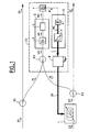
- the resynchronization device shown in the FIG. 1 consists of an adjustable delay device 1, two 1 to 2 couplers K1, K2 and a control unit CU.
- the device receives the input signals E1, E2 and provides resynchronized output signals S1, S2.
- the first input signal El is applied to the input of the first 1 to 2 coupler K1 whose first output provides the first output signal S1 and of which the second output coupled to the CU control unit delivers a first signal measurement optics sl.
- the second input signal E2 is applied to the input of the second coupler K2 by through the delay device 1.
- a first output of coupler K2 provides the second output signal S2 while its second output provides a second signal s2 measurement optics applied to the input of the CU command.
- CU control unit has 2 to 1 coupler K3 whose inputs receive the first and respectively second optical measurement signals s1, s2. Leaving the coupler K3 provides a combination signal s3 which is injected into a non-linear optical device 2.
- the device 2 provides a MO mixing signal to a filter optic F which delivers a filtered signal M to a conversion 5.
- the conversion device 5 provides a control device 8 an electrical control signal C representative of the average signal strength value filtered M.
- the controller 8 provides an electrical control signal CD of the device adjustable delay 1.
- the optical device not linear 2 consists of a fiber optic amplifier 3 coupled to a nonlinear optical medium 4.
- amplifier 3 has the function of injecting into non-linear medium 4 sufficient optical power to bring up intermodulation phenomena research.
- the most suitable nonlinear medium 4 is typically consisting of a semiconductor optical amplifier for which an input optical power of the milliwatt order may be suitable. We could however use other media with properties not linear due to the Kerr effect, such as fibers optical.
- the signals measurement optics s1, s2 have the same polarization.
- the received signals have polarizations we can always plan ahead of the device a known type polarization controller (not represented).
- the conversion device 5 consists of a photodetector 6, for example a photodiode, followed by a low pass electric filter 7.
- the device of figure 1 works in the way next.
- the first optical input signal E1 is received by the first coupler K1 which takes part S1 of the strength of this signal. This part S1 is guided towards a coupler 2 to 1 inputs K3.
- the second signal input E2 passes through delay device 1 to constitute a delayed signal S2 which is injected at the input of the second 1 to 2 coupler K2.
- the coupler K2 takes part s2 of the power of this signal S2 and this part s2 is guided to the other input of the K3 coupler.
- the K3 coupler then provides a combination signal s3 of the signals sl and s2.
- the combination signal s3 is amplified by amplifier 3 so as to provide a signal amplified combination s4 in the nonlinear medium 4.
- the nonlinear medium 4 provides a MO mixing signal containing intermodulation signals whose frequencies optics are of the form p.f1 + q.f2, where p and q are integers relative (and such that the expression is positive).
- Each of the intermodulation signals has a intensity modulation which depends on both modulations intensity of input signals and phase shift of their respective modulation clocks.
- the signal from mixture MO then passes through the filter F which is chosen for transmit an optical frequency band centered on a only intermodulation frequencies f3 and different from f1 and f2.
- the filter F provides the filtered signal M which therefore represents only one of the intermodulation signals.
- the photodetector 6 receives the filtered signal M and provides the low-pass filter 7 with a signal electric detection MC.
- the low-pass filter 7 delivers the electric control signal C which measures the intensity mean optics of the filtered signal M and is therefore representative of the difference between the phases of the clocks of modulation of signals E1 and S2.
- Signal C can then be processed by a type electronic control device conventional 8 designed to control the delay device 1 as a function of signal C so as to impose an offset of phase determined by a Ref.
- the choice of the values of p and q which defines the filter F will be guided by the following considerations.
- the condition necessary is that the frequency f3 is different at the same time of f1 and f2, but it is also desirable that the frequency f3 is in the same frequency range as f1 and f2 of so that you can use an F filter and a photodetector 6 conventional.
- the difference between f1 and f2 is in practice very small compared to f1 or f2
- we will have f3 neighbor of f1 and f2 if we respect the relation p + q 1, with absolute values of p and q of low values.
- Another aspect of implementation concerns the function of filtering carried out by the conversion device 5 so to constitute a device for measuring the average value of the optical intensity of the filtered signal M.
- the constant of conversion device 5 time must be sufficient to do this average. In each particular case it can be evaluated experimentally or by simulations. Thus, for the usual cases of transmission optics, we could for example choose a constant of time in the order of the time interval corresponding to the transmission of a few thousand bits of signals entry.
- the photodetector 6 can already realize a low-pass filtering function, supplemented if necessary by an additional electric low-pass filter 7, as shown in the example in Figure 1.
- the curve of figure 2 represents in percentage the level of the electrical control signal C as a function of ⁇ T in the case where the extinction rate of the signals E1 and E2 is very high.
- Figure 3 shows a similar curve for a TE extinction rate of 13dB. These curves show that the signal C has a maximum value when the offset ⁇ T is zero and a minimum value when ⁇ T is half of the bit T time interval of signals E1 and E2.
- simulations for example allow to establish the law of variation C in function of ⁇ T.
- This law therefore establishes with respect to ⁇ T the transfer function of the set constituted by the devices 2 and 5 in cascade. It is then easy to design a control circuit 8 capable of controlling the delay device 1 so as to impose a value determined (to within T) of the offset ⁇ T.
- control device 8 having for effect of enslaving C to its maximum value. If necessary, we may always impose a determined gap between phases of the two output signals S1 and S2 with a additional delay device (not shown) in output of one of the couplers K1 or K2.
- a realization of the control device 8 can be a circuit well known in the field of regulation which overlaps with low frequency overmodulation to the CD control signal and adjusts this CD control signal so as to make minimum the modulation of the resulting control signal C.
- the variable delay device 1 can be one of the fine adjustment devices commonly used in optical systems.
- a device uses a fiber optic coil, the diameter of which can be modified by a piezoelectric actuator.
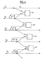
- Figure 4 illustrates how the resynchronization according to the invention can be used for resynchronize between them more than two optical signals, by examples of signals extracted from a length multiplex wave by demultiplexing.
- the assembly shown is organized in several stages receiving by way of example five input signals E1-E5 and providing five resynchronized output signals S1-S5.
- the first two input signals E1, E2 are resynchronized by the first stage which provides the second S2 output signal by means of a first unit of CU1 control arranged in accordance with Figure 1 described previously.
- a second floor with a second unit CU2 resynchronizes the third input signal E3 with respect to the second output signal S2 by providing the third output signal S3.
- a third CU3 control unit resynchronizes S3 and E4 and a fourth control unit CU4 resynchronizes S4 and E5.
- the only adaptation to be envisaged compared to the diagram of the Figure 1 is to provide 1 to 3 couplers at the output delay devices on each stage so as to draw each delayed signal S2-S5 to two units of orders.
- the device that comes to be described is particularly effective in the case where the modulations of the signals E1 and E2 are of type RZ or of soliton type.
- the device can nevertheless be used for NRZ modulations if the input signals present sequences with a large number of frequency transitions bit. Such sequences can for example be sent voluntarily during system initialization.
- the device is not limited to the case where the clock frequencies of the signals input are equal.
- the device can also work if the input signals each have a period whole multiple clock of a common base period.
- the curve representing the variations of the control signal C according to ⁇ T then have several values different amplitudes. This curve can be however, operated by suitable control means 8.
Abstract
Description
L'invention se situe dans le domaine des réseaux de télécommunication et concerne plus particulièrement les systèmes de communication optiques dans lesquels s'effectuent la transmission, le routage et le traitement optiques de données numériques optiques.The invention relates to the field of telecommunications and relates more particularly to optical communication systems in which transmission, routing and processing take place optical digital optical data.
Généralement, les informations véhiculées dans ces systèmes sont des données binaires ayant la forme d'impulsions rythmées à une fréquence d'horloge de modulation déterminée. Les niveaux d'amplitude de ces impulsions sont représentatifs de ces données binaires. Initialement, ces impulsions sont sous forme électrique, puis elles sont converties en un signal optique au moyen d'une modulation d'intensité (puissance optique) d'une onde porteuse optique.Generally, the information conveyed in these systems are binary data having the form of rhythmic pulses at a clock frequency of determined modulation. The amplitude levels of these pulses are representative of this binary data. Initially, these pulses are in electrical form, then they are converted into an optical signal using intensity modulation (optical power) of a wave optical carrier.
Pour que le système puisse transporter un grand nombre de signaux optiques en exploitant la bande passante des liaisons optiques, on utilise des techniques de multiplexage telles que le multiplexage temporel et/ou le multiplexage en longueur d'onde.So that the system can carry a large number of optical signals by exploiting the bandwidth of optical links, we use multiplexing techniques such as time multiplexing and / or multiplexing in wave length.
D'une façon générale, dans la plupart des systèmes de communication optiques impliquant plusieurs longueurs d'onde, il est souhaitable, au moins en certains points du réseau, que plusieurs signaux optiques présentent des modulations d'intensité qui respectent des relations de phase parfaitement définies (à 2π près).In general, in most systems of optical communications involving multiple lengths wave, it is desirable, at least at certain points in the network, that several optical signals have intensity modulations which respect relations of perfectly defined phase (to within 2π).
Ce problème se pose par exemple dans les noeuds de jonction où plusieurs signaux optiques portés par des longueurs d'onde différentes et issus de sources indépendantes doivent être parfaitement synchronisés avant d'être combinés pour former un multiplex de longueurs d'onde.This problem arises for example in the nodes of junction where several optical signals carried by different wavelengths from sources independent must be perfectly synchronized before to be combined to form a multiplex of lengths wave.
Un problème analogue se pose lorsqu'on veut régénérer simultanément des trains de solitons multiplexés en longueur d'onde au moyen d'un modulateur. Pour cela, il faut en effet resynchroniser les trains de solitons avant de les injecter dans le modulateur et commander ce dernier par un signal d'horloge synchrone avec celles des trains de solitons.A similar problem arises when we want to regenerate simultaneously trains of solitons multiplexed in length wave using a modulator. For that, it is indeed necessary resynchronize the soliton trains before injecting them in the modulator and control it with a signal clock synchronous with those of the soliton trains.
Un autre cas est celui des interfaces de multiplexage temporel où plusieurs signaux optiques sont entrelacés temporellement avant d'être combinés pour former le multiplex temporel.Another case is that of multiplexing interfaces temporal where several optical signals are interlaced temporally before being combined to form the time multiplex.
Une solution envisageable consiste à récupérer les horloges associées aux différents signaux à synchroniser, à comparer leurs phases et à appliquer aux signaux des retards fonction de ces comparaisons. Cette solution présente cependant l'inconvénient de nécessiter plusieurs récupérations d'horlogeOne possible solution is to recover the clocks associated with the various signals to be synchronized, compare their phases and apply delays to signals based on these comparisons. This solution presents however the disadvantage of requiring several clock recoveries
Aussi, un des buts de l'invention est de proposer une solution au problème de synchronisation qui évite l'inconvénient précédent. Un autre but est de permette une mise en oeuvre simple aussi bien pour la partie optique qu'au niveau des circuits électroniques associés.Also, one of the aims of the invention is to propose a solution to the synchronization problem which avoids the previous drawback. Another purpose is to allow simple implementation as well for the optical part than at the associated electronic circuits.
Plus précisément, l'invention a pour objet un procédé de resynchronisation de signaux optiques selon lequel un retard ajustable est appliqué à l'un parmi des premier et second signaux optiques d'entrée pour fournir un signal optique retardé calé en phase par rapport à l'autre signal optique d'entrée, lesdits premier et second signaux optiques d'entrée véhiculant des informations par modulations d'intensité d'ondes porteuses optiques ayant des fréquences optiques f1 et f2 différentes, ledit procédé étant caractérisé en ce qu'il consiste :
- à former des premier et second signaux optiques de mesure représentatifs respectivement dudit signal optique retardé et dudit autre signal optique d'entrée,
- à former un signal de combinaison en couplant lesdits premier et second signaux optiques de mesure,
- à former un signal de mélange en injectant ledit signal de combinaison dans un dispositif optique non linéaire,
- à former un signal filtré en filtrant ledit signal de mélange par un filtre calé sur une fréquence optique f3 égale à p.f1 + q.f2, p et q étant des nombres entiers relatifs tels que la fréquence f3 soit différente des fréquences f1 et f2 des ondes porteuses,
- à former un signal électrique de contrôle représentatif de la valeur moyenne de l'intensité dudit signal filtré et
- à commander ledit retard ajustable en fonction dudit signal de contrôle.
- forming first and second optical measurement signals representative respectively of said delayed optical signal and of said other optical input signal,
- forming a combination signal by coupling said first and second optical measurement signals,
- forming a mixing signal by injecting said combination signal into a non-linear optical device,
- forming a filtered signal by filtering said mixing signal by a filter calibrated on an optical frequency f3 equal to p.f1 + q.f2, p and q being relative integers such that the frequency f3 is different from the frequencies f1 and f2 carrier waves,
- forming an electrical control signal representative of the average value of the intensity of said filtered signal and
- controlling said adjustable delay as a function of said control signal.
Ainsi, le procédé exploite la propriété des milieux optiques non linéaires d'être le siège de phénomènes d'intermodulation lorsque par exemple deux signaux optiques de fréquences porteuses différentes f1, f2 y sont introduits. Le milieu engendre alors des signaux d'intermodulation portés par des fréquences optiques de la forme p.f1 + q.f2, p et q étant dans le cas général des nombres entiers relatifs qui rendent bien entendu l'expression précédente positive. L'amplitude de la modulation de chacun de ces signaux est notamment représentative de l'écart entre les phases des signaux introduits. Les essais ont montré que la valeur moyenne de l'intensité d'un signal d'intermodulation choisi représente bien cet écart de phase.Thus, the process exploits the property of the media nonlinear optics to be the seat of phenomena intermodulation when for example two optical signals of different carrier frequencies f1, f2 are there introduced. The medium then generates signals intermodulation carried by optical frequencies of the form p.f1 + q.f2, p and q being in the general case of relative integers which of course make the previous positive expression. The amplitude of the modulation of each of these signals is notably representative of the difference between the phases of the signals introduced. Tests have shown that the average value of the intensity of a selected intermodulation signal represents well this phase deviation.
Le procédé s'effectue en partie dans le domaine optique et en partie dans le domaine électrique avec l'avantage que le traitement dans le domaine électrique ne nécessite aucun circuit devant travailler à haute fréquence, ce qui simplifie considérablement la réalisation.The process is partly carried out in the field optics and partly in the electrical field with the advantage that the treatment in the electrical field does requires no circuit to work at high frequency, which considerably simplifies implementation.
Le procédé défini ci-dessus permet aussi de resynchroniser plus de deux signaux. Il suffit par exemple d'appliquer le procédé à deux premiers signaux, ce qui fournit deux signaux de sortie resynchronisés, puis d'appliquer à nouveau le procédé à un troisième signal et à l'un des deux premiers signaux de sortie resynchronisés, et ainsi de suite. The process defined above also makes it possible to resynchronize more than two signals. It suffices for example to apply the process to the first two signals, which provides two resynchronized output signals and then to apply the process again to a third signal and to one of the first two resynchronized output signals, and and so on.
Selon une variante préférée, lesdits nombres p et q sont tels que l'écart entre ladite fréquence f3 du filtre et l'une des fréquences f1 ou f2 des ondes porteuses soit égal à l'écart entre lesdites fréquences f1 et f2 des ondes porteuses.According to a preferred variant, said numbers p and q are such that the difference between said frequency f3 of the filter and one of the frequencies f1 or f2 of the carrier waves is equal away from said frequencies f1 and f2 of the waves carriers.
Cette dernière disposition assure que la fréquence f3 est voisine des fréquences f1 et f2, c'est-à-dire se situe dans la gamme usuelle des fréquences optiques utilisée en transmission. Ainsi les éléments optiques traitant le signal de mélange (filtre, photodétecteur) peuvent être de types conventionnels.This latter arrangement ensures that the frequency f3 is close to frequencies f1 and f2, i.e. is located in the usual range of optical frequencies used in transmission. Thus the optical elements processing the signal of mixing (filter, photodetector) can be of types conventional.
Selon un autre aspect de l'invention, le procédé est en outre caractérisé en ce que lesdits premier et second signaux optiques de mesure sont prélevées respectivement dudit signal optique retardé et dudit autre signal optique d'entrée et en ce que ledit signal de combinaison est amplifié optiquement avant d'être injecté dans un milieu optique non linéaire.According to another aspect of the invention, the method is further characterized in that said first and second optical measurement signals are taken respectively of said delayed optical signal and of said other optical signal input and in that said combination signal is optically amplified before being injected into a medium nonlinear optics.
Selon encore un autre aspect, ledit signal électrique de contrôle est obtenu par un filtrage passe-bas électrique d'un signal converti fourni par un photodétecteur auquel est appliqué ledit signal filtré.According to yet another aspect, said electrical signal control is obtained by electric low pass filtering of a converted signal supplied by a photodetector which is applied said filtered signal.
L'invention a également pour objet un dispositif de resynchronisation de signaux optiques pour la mise en oeuvre du procédé définit ci-dessus. Le dispositif de resynchronisation comporte un dispositif à retard ajustable disposé pour recevoir l'un parmi des premier et second signaux optiques d'entrée et apte à fournir un signal optique retardé calé en phase par rapport à l'autre signal optique d'entrée, lesdits premier et second signaux optiques d'entrée véhiculant des informations par modulations d'intensité d'ondes porteuses optiques ayant des fréquences optiques f1 et f2 différentes. Le dispositif est caractérisé en ce qu'il comprend :
- des moyens de prélèvement pour former des premier et second signaux optiques de mesure représentatifs respectivement dudit signal optique retardé et dudit autre signal optique d'entrée,
- des moyens de couplage disposés pour recevoir lesdits premier et second signaux optiques de mesure et apte à fournir un signal de combinaison,
- un dispositif optique non linéaire disposé pour recevoir ledit signal de combinaison et apte à fournir un signal de mélange,
- un filtre disposé pour recevoir ledit signal de mélange et apte à fournir un signal filtré, ledit filtre étant calé sur une fréquence optique f3 égale à p.f1 + q.f2, p et q étant des nombres entiers relatifs tels que la fréquence f3 soit différente des fréquences f1 et f2 des ondes porteuses,
- un dispositif de conversion pour former un signal électrique de contrôle représentatif de la valeur moyenne de l'intensité dudit signal filtré et
- des moyens de commande pour commander ledit dispositif à retard ajustable en fonction dudit signal de contrôle.
- sampling means for forming first and second optical measurement signals representative respectively of said delayed optical signal and of said other optical input signal,
- coupling means arranged to receive said first and second optical measurement signals and capable of providing a combination signal,
- a non-linear optical device arranged to receive said combination signal and capable of providing a mixing signal,
- a filter arranged to receive said mixing signal and capable of providing a filtered signal, said filter being calibrated on an optical frequency f3 equal to p.f1 + q.f2, p and q being relative integers such that the frequency f3 is different from the frequencies f1 and f2 of the carrier waves,
- a conversion device for forming an electrical control signal representative of the average value of the intensity of said filtered signal and
- control means for controlling said adjustable delay device as a function of said control signal.
D'autres aspects et avantages de l'invention apparaítront dans la suite de la description en référence aux figures.
- La figure 1 représente un mode de réalisation du dispositif de resynchronisation selon l'invention.
- Les figures 2 et 3 sont des courbes représentant les variations relatives du signal de contrôle en fonction du décalage entre les phases des signaux optiques.
- La figure 4 représente un montage pour resynchroniser entre eux plus de deux signaux optiques et dans lequel est utilisé le dispositif selon l'invention.
- FIG. 1 represents an embodiment of the resynchronization device according to the invention.
- FIGS. 2 and 3 are curves representing the relative variations of the control signal as a function of the offset between the phases of the optical signals.
- FIG. 4 represents an arrangement for resynchronizing between them more than two optical signals and in which the device according to the invention is used.
Le dispositif de resynchronisation représenté sur la
figure 1 est constitué d'un dispositif à retard ajustable 1,
de deux coupleurs 1 vers 2 K1, K2 et d'une unité de commande
CU.The resynchronization device shown in the
FIG. 1 consists of an
Le dispositif reçoit les signaux d'entrée E1, E2 et
fournit des signaux de sortie resynchronisés S1, S2. Le
premier signal d'entrée El est appliqué à l'entrée du
premier coupleur 1 vers 2 K1 dont la première sortie fournit
le premier signal de sortie S1 et dont la deuxième sortie
couplée à l'unité de commande CU délivre un premier signal
optique de mesure sl. Le second signal d'entrée E2 est
appliqué à l'entrée du second coupleur K2 par
l'intermédiaire du dispositif à retard 1. Une première
sortie du coupleur K2 fournit le second signal de sortie S2
tandis que sa seconde sortie fournit un second signal
optique de mesure s2 appliqué à l'entrée de l'unité de
commande CU.The device receives the input signals E1, E2 and
provides resynchronized output signals S1, S2. The
first input signal El is applied to the input of the
first 1 to 2 coupler K1 whose first output provides
the first output signal S1 and of which the second output
coupled to the CU control unit delivers a first signal
measurement optics sl. The second input signal E2 is
applied to the input of the second coupler K2 by
through the
L'unité de commande CU comporte un coupleur 2 vers 1
K3 dont les entrées reçoivent respectivement les premiers et
second signaux optiques de mesure s1, s2. La sortie du
coupleur K3 fournit un signal de combinaison s3 qui est
injecté dans un dispositif optique non linéaire 2. Le
dispositif 2 fournit un signal de mélange MO à un filtre
optique F qui délivre un signal filtré M à un dispositif de
conversion 5. Le dispositif de conversion 5 fournit à un
dispositif de commande 8 un signal électrique de contrôle C
représentatif de la valeur moyenne de l'intensité du signal
filtré M. En réponse au signal C, le dispositif de commande
8 fournit un signal électrique de commande CD du dispositif
à retard ajustable 1.CU control unit has 2 to 1 coupler
K3 whose inputs receive the first and respectively
second optical measurement signals s1, s2. Leaving the
coupler K3 provides a combination signal s3 which is
injected into a non-linear
Dans l'exemple représenté, le dispositif optique non
linéaire 2 est constitué d'un amplificateur optique à fibre
3 couplé à un milieu optique non linéaire 4. Comme les
signaux de mesure sl et s2 prélevés des signaux d'entrée E1
et E2 présentent des puissances optiques relativement
faibles, l'amplificateur 3 a pour fonction d'injecter dans
le milieu non linéaire 4 une puissance optique suffisante
pour faire apparaítre les phénomènes d'intermodulation
recherchés. Le milieu non linéaire 4 le plus approprié est
typiquement constitué d'un amplificateur optique semi-conducteur
pour lequel une puissance optique d'entrée de
l'ordre du milliwatt peut convenir. On pourrait cependant
utiliser d'autres milieux présentant des propriétés non
linéaires dues à l'effet Kerr, comme par exemple les fibres
optiques.In the example shown, the optical device not
linear 2 consists of a
Il est par ailleurs préférable que les signaux optiques de mesure s1, s2 présentent la même polarisation. Au cas où les signaux reçus auraient des polarisations différentes, on pourra toujours prévoir en amont du dispositif un contrôleur de polarisation de type connu (non représenté).It is also preferable that the signals measurement optics s1, s2 have the same polarization. In case the received signals have polarizations we can always plan ahead of the device a known type polarization controller (not represented).
Le dispositif de conversion 5 est constitué d'un photodétecteur 6, par exemple une photodiode, suivi d'un filtre électrique passe-bas 7.The conversion device 5 consists of a photodetector 6, for example a photodiode, followed by a low pass electric filter 7.
Le dispositif de la figure 1 fonctionne de la façon
suivante. Le premier signal optique d'entrée E1 est reçu par
le premier coupleur K1 qui prélève une partie S1 de la
puissance de ce signal. Cette partie S1 est guidée vers une
des entrées du coupleur 2 vers 1 K3. Le second signal
d'entrée E2 traverse le dispositif à retard 1 pour constitué
un signal retardé S2 qui est injecté à l'entrée du second
coupleur 1 vers 2 K2. Le coupleur K2 prélève une partie s2
de la puissance de ce signal S2 et cette partie s2 est
guidée vers l'autre entrée du coupleur K3. Le coupleur K3
fournit alors un signal de combinaison s3 des signaux sl et
s2. Le signal de combinaison s3 est amplifié par
l'amplificateur 3 de façon à fournir un signal de
combinaison amplifiée s4 au milieu non linéaire 4.The device of figure 1 works in the way
next. The first optical input signal E1 is received by
the first coupler K1 which takes part S1 of the
strength of this signal. This part S1 is guided towards a
Les porteuses des signaux d'entrée E1 et E2 ayant des
fréquences optiques f1 et f2 supposées différentes, le
milieu non linéaire 4 fournit un signal de mélange MO
contenant des signaux d'intermodulation dont les fréquences
optiques sont de la forme p.f1 + q.f2, où p et q sont des
nombres entiers relatifs (et tels que l'expression soit
positive). Chacun des signaux d'intermodulation présente une
modulation d'intensité qui dépend à la fois des modulations
d'intensité des signaux d'entrées et du décalage de phase de
leurs horloges de modulation respectives. Le signal de
mélange MO traverse alors le filtre F qui est choisi pour
transmettre une bande de fréquence optique centrée sur une
seule des fréquences d'intermodulation f3 et différente de
f1 et de f2. Le filtre F fournit le signal filtré M qui
représente donc un seul des signaux d'intermodulation.The carriers of the input signals E1 and E2 having
optical frequencies f1 and f2 assumed to be different, the
Le photodétecteur 6 reçoit le signal filtré M et
fournit au filtre passe-bas électrique 7 un signal
électrique de détection MC. Le filtre passe-bas 7 délivre le
signal électrique de contrôle C qui mesure l'intensité
optique moyenne du signal filtré M et est par conséquent
représentatif du décalage entre les phases des horloges de
modulation des signaux E1 et S2. Le signal C peut alors être
traité par un dispositif électronique de commande de type
conventionnel 8 conçu pour piloter le dispositif à retard 1
en fonction du signal C de façon à imposer un décalage de
phase déterminé par une consigne Ref.The photodetector 6 receives the filtered signal M and
provides the low-pass filter 7 with a signal
electric detection MC. The low-pass filter 7 delivers the
electric control signal C which measures the intensity
mean optics of the filtered signal M and is therefore
representative of the difference between the phases of the clocks of
modulation of signals E1 and S2. Signal C can then be
processed by a type electronic control device
conventional 8 designed to control the
Le choix des valeurs de p et q qui définit le filtre F sera guidé par les considérations suivantes. La condition nécessaire est que la fréquence f3 soit différente à la fois de f1 et f2, mais il est aussi souhaitable que la fréquence f3 soit dans la même gamme de fréquence que f1 et f2 de façon à pouvoir utiliser un filtre F et un photodétecteur 6 conventionnels. Compte tenu du fait que l'écart entre f1 et f2 est en pratique très petit par rapport à f1 ou f2, on aura f3 voisin de f1 et f2 si on respecte la relation p + q = 1, avec des valeurs absolues de p et q de faibles valeurs.The choice of the values of p and q which defines the filter F will be guided by the following considerations. The condition necessary is that the frequency f3 is different at the same time of f1 and f2, but it is also desirable that the frequency f3 is in the same frequency range as f1 and f2 of so that you can use an F filter and a photodetector 6 conventional. Taking into account that the difference between f1 and f2 is in practice very small compared to f1 or f2, we will have f3 neighbor of f1 and f2 if we respect the relation p + q = 1, with absolute values of p and q of low values.
Il convient aussi de tenir compte des propriétés du milieu non linéaire utilisé en choisissant p et q pour que la puissance du signal d'intermodulation correspondant soit la plus élevée possible. Ainsi, dans le cas où le milieu non linéaire est un amplificateur optique semi-conducteur la plus forte puissance est obtenue pour p = 2 et q = -1 ou bien pour q = 2 et p = -1.The properties of the nonlinear medium used by choosing p and q so that the strength of the corresponding intermodulation signal either as high as possible. So, in case the middle not linear is a semiconductor optical amplifier the higher power is obtained for p = 2 and q = -1 or good for q = 2 and p = -1.
Un autre aspect de réalisation concerne la fonction de filtrage réalisée par le dispositif de conversion 5 de façon à constituer un dispositif de mesure de la valeur moyenne de l'intensité optique du signal filtré M. La constante de temps du dispositif de conversion 5 doit être suffisante pour effectuer cette moyenne. Dans chaque cas particulier elle pourra être évaluée expérimentalement ou par simulations. Ainsi, pour les cas usuels de transmission optique, on pourra par exemple choisir une constante de temps de l'ordre de l'intervalle de temps correspondant à la transmission de quelques milliers de bits des signaux d'entrée.Another aspect of implementation concerns the function of filtering carried out by the conversion device 5 so to constitute a device for measuring the average value of the optical intensity of the filtered signal M. The constant of conversion device 5 time must be sufficient to do this average. In each particular case it can be evaluated experimentally or by simulations. Thus, for the usual cases of transmission optics, we could for example choose a constant of time in the order of the time interval corresponding to the transmission of a few thousand bits of signals entry.
En pratique, le photodétecteur 6 peut déjà réaliser une fonction de filtrage passe-bas, complétée si nécessaire par un filtre passe-bas électrique supplémentaire 7, comme représenté dans l'exemple de la figure 1.In practice, the photodetector 6 can already realize a low-pass filtering function, supplemented if necessary by an additional electric low-pass filter 7, as shown in the example in Figure 1.
Des exemples de relation entre le décalage temporel ΔT entre deux fronts d'horloges successifs des signaux E1 et E2 et le signal C fournit par le dispositif 5 sont illustrés par les figures 2 et 3.Examples of the relationship between the time difference ΔT between two successive clock fronts of signals E1 and E2 and the signal C supplied by the device 5 are illustrated by Figures 2 and 3.
La courbe de la figure 2 représente en pourcentage le niveau du signal électrique de contrôle C en fonction de ΔT dans le cas où le taux d'extinction des signaux E1 et E2 est très élevé. La figure 3 représente une courbe analogue pour un taux d'extinction TE de 13dB. Ces courbes montrent que le signal C présente une valeur maximale lorsque le décalage ΔT est nul et une valeur minimale lorsque ΔT vaut la moitié de l'intervalle de temps bit T des signaux E1 et E2.The curve of figure 2 represents in percentage the level of the electrical control signal C as a function of ΔT in the case where the extinction rate of the signals E1 and E2 is very high. Figure 3 shows a similar curve for a TE extinction rate of 13dB. These curves show that the signal C has a maximum value when the offset ΔT is zero and a minimum value when ΔT is half of the bit T time interval of signals E1 and E2.
Ainsi, pour chaque cas particulier, des simulations
par exemple permettent d'établir la loi de variation C en
fonction de ΔT. Cette loi établit donc par rapport à ΔT la
fonction de transfert de l'ensemble constitué par les
dispositifs 2 et 5 en cascade. Il est alors aisé de
concevoir un circuit de commande 8 apte à commander le
dispositif à retard 1 de façon à imposer une valeur
déterminée (à T près) du décalage ΔT.So, for each particular case, simulations
for example allow to establish the law of variation C in
function of ΔT. This law therefore establishes with respect to ΔT the
transfer function of the set constituted by the
Toutefois, pour échapper à l'influence du taux
d'extinction TE sur la loi de variation de C, on aura
intérêt à concevoir un dispositif de commande 8 ayant pour
effet d'asservir C à sa valeur maximale. Si nécessaire, on
pourra toujours imposer un décalage déterminé entre les
phases des deux signaux de sortie S1 et S2 en disposant un
dispositif à retard supplémentaire (non représenté) en
sortie de l'un des coupleurs K1 ou K2. Dans ce cas, une
réalisation du dispositif de commande 8 peut être un circuit
bien connu dans le domaine de la régulation qui superpose à
au signal de commande CD une surmodulation à basse fréquence
et ajuste ce signal de commande CD de façon à rendre minimum
la modulation du signal de contrôle C qui en résulte.However, to escape the influence of the rate
extinction TE on the law of variation of C, we will have
interest in designing a
Le dispositif à retard variable 1 peut être un des
dispositifs à réglage fin couramment employés dans les
systèmes optiques. Par exemple, un tel dispositif utilise
une bobine de fibre optique, dont le diamètre peut être
modifié par un actionneur piézo-électrique.The
La figure 4 illustre comment le dispositif de resynchronisation selon l'invention peut être utilisé pour resynchroniser entre eux plus de deux signaux optiques, par exemples des signaux extraits d'un multiplex de longueurs d'onde par démultiplexage.Figure 4 illustrates how the resynchronization according to the invention can be used for resynchronize between them more than two optical signals, by examples of signals extracted from a length multiplex wave by demultiplexing.
Le montage représenté est organisé en plusieurs étages recevant à titre d'exemple cinq signaux d'entrée E1-E5 et fournissant cinq signaux de sorties resynchronisés S1-S5. Les deux premiers signaux d'entrées E1, E2 sont resynchronisés par le premier étage qui fournit le deuxième signal de sortie S2 au moyen d'une première unité de commande CU1 disposée conformément à la figure 1 décrite précédemment. Un second étage comportant une seconde unité de commande CU2 resynchronise le troisième signal d'entrée E3 par rapport au second signal de sortie S2 en fournissant le troisième signal de sortie S3. De même, une troisième unité de commande CU3 resynchronise S3 et E4 et une quatrième unité de commande CU4 resynchronise S4 et E5. La seule adaptation à prévoir par rapport au schéma de la figure 1 consiste à prévoir des coupleurs 1 vers 3 en sortie des dispositifs à retard de chaque étage de façon à prélever chaque signal retardé S2-S5 à destination de deux unités de commandes.The assembly shown is organized in several stages receiving by way of example five input signals E1-E5 and providing five resynchronized output signals S1-S5. The first two input signals E1, E2 are resynchronized by the first stage which provides the second S2 output signal by means of a first unit of CU1 control arranged in accordance with Figure 1 described previously. A second floor with a second unit CU2 resynchronizes the third input signal E3 with respect to the second output signal S2 by providing the third output signal S3. Likewise, a third CU3 control unit resynchronizes S3 and E4 and a fourth control unit CU4 resynchronizes S4 and E5. The only adaptation to be envisaged compared to the diagram of the Figure 1 is to provide 1 to 3 couplers at the output delay devices on each stage so as to draw each delayed signal S2-S5 to two units of orders.
Il convient de noter que le dispositif qui vient d'être décrit est particulièrement efficace dans le cas où les modulations des signaux E1 et E2 sont de type RZ ou de type soliton. Le dispositif est néanmoins utilisable pour des modulations NRZ si les signaux d'entrée présentent des séquences ayant un grand nombre de transition à la fréquence bit. De telles séquences peuvent par exemple être envoyées volontairement au cours de l'initialisation du système.It should be noted that the device that comes to be described is particularly effective in the case where the modulations of the signals E1 and E2 are of type RZ or of soliton type. The device can nevertheless be used for NRZ modulations if the input signals present sequences with a large number of frequency transitions bit. Such sequences can for example be sent voluntarily during system initialization.
Il faut aussi signaler que le dispositif n'est pas limité au cas où les fréquences d'horloges des signaux d'entrée sont égales. Le dispositif peut fonctionner aussi si les signaux d'entrée possèdent chacun une période d'horloge multiple entier d'une période de base commune. La courbe représentant les variations du signal de contrôle C en fonction de ΔT présentent alors plusieurs valeurs maximales d'amplitudes différentes. Cette courbe peut être cependant exploitée par des moyens de commande 8 adaptés.It should also be noted that the device is not limited to the case where the clock frequencies of the signals input are equal. The device can also work if the input signals each have a period whole multiple clock of a common base period. The curve representing the variations of the control signal C according to ΔT then have several values different amplitudes. This curve can be however, operated by suitable control means 8.
Claims (10)
Applications Claiming Priority (2)
| Application Number | Priority Date | Filing Date | Title |
|---|---|---|---|
| FR9801675A FR2774832B1 (en) | 1998-02-12 | 1998-02-12 | METHOD AND DEVICE FOR RESYNCHRONIZING OPTICAL SIGNALS |
| FR9801675 | 1998-02-12 |
Publications (1)
| Publication Number | Publication Date |
|---|---|
| EP0936773A1 true EP0936773A1 (en) | 1999-08-18 |
Family
ID=9522886
Family Applications (1)
| Application Number | Title | Priority Date | Filing Date |
|---|---|---|---|
| EP99400322A Withdrawn EP0936773A1 (en) | 1998-02-12 | 1999-02-11 | Method and device for resynchronisation of optical signals |
Country Status (5)
| Country | Link |
|---|---|
| US (1) | US6424443B1 (en) |
| EP (1) | EP0936773A1 (en) |
| JP (1) | JPH11317704A (en) |
| CA (1) | CA2259017A1 (en) |
| FR (1) | FR2774832B1 (en) |
Cited By (3)
| Publication number | Priority date | Publication date | Assignee | Title |
|---|---|---|---|---|
| WO2001050664A2 (en) * | 1999-12-30 | 2001-07-12 | Siemens Aktiengesellschaft | Method for synchronising the phase of optical return-to-zero (rz) data signals |
| EP1176751A1 (en) * | 2000-07-27 | 2002-01-30 | Alcatel | Synchronizer for RZ-WDM signals and method for synchronisation |
| EP1233567A1 (en) * | 2001-01-25 | 2002-08-21 | Alcatel | Method for adjusting time delays and device for synchronization of channels in a WDM system |
Families Citing this family (2)
| Publication number | Priority date | Publication date | Assignee | Title |
|---|---|---|---|---|
| US10892822B2 (en) * | 2017-02-01 | 2021-01-12 | British Telecommunications Public Limited Company | Optical fiber event location |
| US11274990B2 (en) | 2017-07-20 | 2022-03-15 | British Telecommunications Public Limited Company | Optical fiber |
Citations (3)
| Publication number | Priority date | Publication date | Assignee | Title |
|---|---|---|---|---|
| EP0619658A2 (en) * | 1993-04-09 | 1994-10-12 | Nec Corporation | Apparatus for extracting an optical clock and apparatus for demultiplexing a time-division multiplexed signal |
| US5373381A (en) * | 1989-07-21 | 1994-12-13 | Alfano; Robert R. | Terahertz repetition rate optical computing systems, and communication systems and logic elements using cross-phase modulation based optical processors |
| WO1997044929A1 (en) * | 1996-05-22 | 1997-11-27 | British Telecommunications Public Limited Company | Optical synchronisation arrangement |
Family Cites Families (2)
| Publication number | Priority date | Publication date | Assignee | Title |
|---|---|---|---|---|
| IT1276122B1 (en) * | 1995-11-14 | 1997-10-24 | Pirelli Cavi Spa | METHOD AND DEVICE TO OPTICALLY RECOVER THE SYNCHRONISM OF A DIGITAL OPTICAL SIGNAL |
| FR2749946B1 (en) * | 1996-06-14 | 1998-07-31 | Alsthom Cge Alcatel | DEVICE FOR SHAPING BINARY OPTICAL SIGNALS AND ITS USE FOR MODIFYING SAID SIGNALS |
-
1998
- 1998-02-12 FR FR9801675A patent/FR2774832B1/en not_active Expired - Fee Related
-
1999
- 1999-02-01 CA CA002259017A patent/CA2259017A1/en not_active Abandoned
- 1999-02-05 US US09/245,334 patent/US6424443B1/en not_active Expired - Fee Related
- 1999-02-10 JP JP11033452A patent/JPH11317704A/en active Pending
- 1999-02-11 EP EP99400322A patent/EP0936773A1/en not_active Withdrawn
Patent Citations (3)
| Publication number | Priority date | Publication date | Assignee | Title |
|---|---|---|---|---|
| US5373381A (en) * | 1989-07-21 | 1994-12-13 | Alfano; Robert R. | Terahertz repetition rate optical computing systems, and communication systems and logic elements using cross-phase modulation based optical processors |
| EP0619658A2 (en) * | 1993-04-09 | 1994-10-12 | Nec Corporation | Apparatus for extracting an optical clock and apparatus for demultiplexing a time-division multiplexed signal |
| WO1997044929A1 (en) * | 1996-05-22 | 1997-11-27 | British Telecommunications Public Limited Company | Optical synchronisation arrangement |
Cited By (7)
| Publication number | Priority date | Publication date | Assignee | Title |
|---|---|---|---|---|
| WO2001050664A2 (en) * | 1999-12-30 | 2001-07-12 | Siemens Aktiengesellschaft | Method for synchronising the phase of optical return-to-zero (rz) data signals |
| WO2001050664A3 (en) * | 1999-12-30 | 2002-01-31 | Siemens Ag | Method for synchronising the phase of optical return-to-zero (rz) data signals |
| US7312909B2 (en) | 1999-12-30 | 2007-12-25 | Siemens Aktiengesellschaft | Method for synchronizing the phase of optical return-to-zero (RZ) data signals |
| EP1176751A1 (en) * | 2000-07-27 | 2002-01-30 | Alcatel | Synchronizer for RZ-WDM signals and method for synchronisation |
| WO2002011354A1 (en) * | 2000-07-27 | 2002-02-07 | Alcatel | Synchronizer for rz-wdm signals and method for synchronization |
| EP1233567A1 (en) * | 2001-01-25 | 2002-08-21 | Alcatel | Method for adjusting time delays and device for synchronization of channels in a WDM system |
| US7187869B2 (en) | 2001-01-25 | 2007-03-06 | Alcatel | Method for adjusting time delays and device for synchronization of channels in a WDM system |
Also Published As
| Publication number | Publication date |
|---|---|
| FR2774832B1 (en) | 2000-08-04 |
| US6424443B1 (en) | 2002-07-23 |
| CA2259017A1 (en) | 1999-08-12 |
| FR2774832A1 (en) | 1999-08-13 |
| JPH11317704A (en) | 1999-11-16 |
Similar Documents
| Publication | Publication Date | Title |
|---|---|---|
| EP0975107B1 (en) | Transmitting device for optical data | |
| EP1111820A1 (en) | Apparatus for applying a delay | |
| EP0862286B1 (en) | Optical regeneration for optical fibre transmission systems with non-soliton signals | |
| EP0718992B1 (en) | Inline regenerator device of a soliton signal via synchronous solitory modulation using a non-linear optical mirror | |
| FR2761490A1 (en) | Optical time division multiplexer for temperature/pressure sensor | |
| EP0813097B1 (en) | Digital optical signal regeneration device and its use for modifying digital optical signals | |
| EP0763912B1 (en) | All-optical doubler and soliton regenerator using the doubler | |
| FR2762732A1 (en) | METHOD AND DEVICE FOR DECOMPRESSION OF PULSES CONSTITUTING A BINARY OPTICAL SIGNAL | |
| FR2703547A1 (en) | Optical device for recovering the rhythm of a code signal. | |
| EP0936773A1 (en) | Method and device for resynchronisation of optical signals | |
| FR2799070A1 (en) | WAVELENGTH MULTIPLEX OPTICAL SIGNAL REGENERATOR | |
| EP0852436B1 (en) | Very high data rate soliton regenerator | |
| EP0871304B1 (en) | Method and device for forming an optical binary signal | |
| EP0975106B1 (en) | Device for on-line regeneration of an optical soliton signal by synchronous modulation of these solitons and transmission system comprising such a device | |
| EP0746070B1 (en) | Method and device to combine optical signals | |
| FR2797331A1 (en) | OPTICAL DIFFERENTIATOR | |
| EP1158352A2 (en) | Optical NRZ-RZ converter | |
| EP1314267A1 (en) | All-optical regenerator for wavelength-division multiplexed signals | |
| CA2376153A1 (en) | Regenerator with reconstitution of an optical signal carrier wave | |
| EP0652653A1 (en) | Optical fibre telecommunication method, link applying this method and pumping system for four wave mixing, particularly for this link | |
| EP1142168A1 (en) | Device for generating carriers for wavelength-division multiplexing optical transmission system with rz signals | |
| FR2715255A1 (en) | Soliton transmission coding method for optical fibre links |
Legal Events
| Date | Code | Title | Description |
|---|---|---|---|
| PUAI | Public reference made under article 153(3) epc to a published international application that has entered the european phase |
Free format text: ORIGINAL CODE: 0009012 |
|
| AK | Designated contracting states |
Kind code of ref document: A1 Designated state(s): DE FI GB IT SE |
|
| AX | Request for extension of the european patent |
Free format text: AL;LT;LV;MK;RO;SI |
|
| 17P | Request for examination filed |
Effective date: 20000218 |
|
| AKX | Designation fees paid |
Free format text: DE FI GB IT SE |
|
| 17Q | First examination report despatched |
Effective date: 20040421 |
|
| STAA | Information on the status of an ep patent application or granted ep patent |
Free format text: STATUS: THE APPLICATION IS DEEMED TO BE WITHDRAWN |
|
| 18D | Application deemed to be withdrawn |
Effective date: 20041001 |