EP0940909A1 - Digital FM demodulation circuit - Google Patents
Digital FM demodulation circuit Download PDFInfo
- Publication number
- EP0940909A1 EP0940909A1 EP99301461A EP99301461A EP0940909A1 EP 0940909 A1 EP0940909 A1 EP 0940909A1 EP 99301461 A EP99301461 A EP 99301461A EP 99301461 A EP99301461 A EP 99301461A EP 0940909 A1 EP0940909 A1 EP 0940909A1
- Authority
- EP
- European Patent Office
- Prior art keywords
- signal
- arctangent
- value
- circuit
- digital
- Prior art date
- Legal status (The legal status is an assumption and is not a legal conclusion. Google has not performed a legal analysis and makes no representation as to the accuracy of the status listed.)
- Granted
Links
Images

Classifications
-
- H—ELECTRICITY
- H03—ELECTRONIC CIRCUITRY
- H03D—DEMODULATION OR TRANSFERENCE OF MODULATION FROM ONE CARRIER TO ANOTHER
- H03D3/00—Demodulation of angle-, frequency- or phase- modulated oscillations
- H03D3/006—Demodulation of angle-, frequency- or phase- modulated oscillations by sampling the oscillations and further processing the samples, e.g. by computing techniques
-
- G—PHYSICS
- G06—COMPUTING; CALCULATING OR COUNTING
- G06F—ELECTRIC DIGITAL DATA PROCESSING
- G06F1/00—Details not covered by groups G06F3/00 - G06F13/00 and G06F21/00
- G06F1/02—Digital function generators
- G06F1/03—Digital function generators working, at least partly, by table look-up
- G06F1/035—Reduction of table size
- G06F1/0356—Reduction of table size by using two or more smaller tables, e.g. addressed by parts of the argument
Definitions
- the present invention relates to a digital FM demodulation circuit which uses an arctangent circuit having ROM tables.
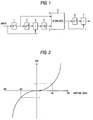
- Fig. 1 is a schematic block diagram showing a conventional digital FM demodulation circuit.
- the digital FM demodulation circuit includes delay circuits 1, 2, and 6, adders 3 and 7, a divider 4, and an arctangent circuit 5. The operation of the digital FM demodulation circuit will be described.
- the demodulation circuit there is inputted a digital FM signal into which an analog FM signal is converted with a sampling frequency that is four times higher than a frequency of the analog signal.
- the sampling frequency When the sampling frequency is set to be four times as large as the frequency of the original signal, it is possible to set a phase difference between the sampling frequency and an non-modulated digital FM signal at 90 degrees. Each time when a digital FM signal is passed through a delay circuit, the phase of the signal is delayed at 90 degrees.
- the sampled digital FM signal passes through a delay circuit 1 to be converted to a second signal that is delayed for a constant time.
- the second signal is referred to as sin ⁇ t .
- the sampled digital FM signal is converted also to a third signal which is always phase-shifted at 90 degrees with respect to the second signal, by a Hilbert conversion circuit including the delay circuits 1 and 2, the adder 3, and the divider 4.
- the third signal is referred to as cos ⁇ t .
- a FM signal S which is not phase-shifted, i.e., sin ⁇ t are inputted to the arctangent circuit 5.
- An output of the arctangent circuit 5 is delayed for one sampling period by the delay circuit 6, and then inverted by an inverting circuit which is not shown.
- the inverted output is supplied to one input of the adder 7.
- the output of the arctangent circuit 5 is directly inputted.
- the two inputs are added to each other, so that a FM detector output as a demodulated signal is obtained.
- a general digital FM demodulation circuit requires an arctangent circuit in which the phase of a sampled signal is calculated from the amplitude of the signal.
- a calculation circuit itself is not configured and the phase is obtained by using ROM tables corresponding to an input value.
- the output digital value is expressed by one bit in code information and n bits in amplitude information.
- code information consists of 1 bit and amplitude information of 3 bits
- the amplitude of the input signal is expressed by one of digital values of 15 kinds from -7 to 7.
- each of the above-mentioned S and C can have one of the values from -7 to 7, and 113 ROM tables of arctangents of S/C are necessary (when S/C ⁇ 0, 64 ROM tables, and when S/C ⁇ 0, 49 ROM tables).
- S/C ⁇ 0, 64 ROM tables and when S/C ⁇ 0, 49 ROM tables.
- a digital FM demodulation circuit sampling an input analog FM signal and digitally detecting the sampled input signal comprising:
- the arctangent circuit may further comprise:
- the arctangent circuit may further comprise:
- Table 1 shows values of S/C in the case where S and C may be one of 0 to 7 (3 bits).
- the S/C axis of the graph of Fig. 2 is equally divided.
- the above-described first technique it is only required to consider the first quadrant of Fig. 2.
- infinite values exist in the range of S/C > 1. Therefore, the S/C axis cannot be equally divided. Therefore, it is assumed that also the above-described second technique is further used. In this case, it is only required to consider the range of the arctangent value from 0 to 45 degrees. In this range (0 ⁇ S/C ⁇ 1), therefore, the S/C axis can be equally divided.
- Table 2 below is a table where values of S/C which is not larger than 1 are arranged in ascending order.
- each value of the column of "phase difference from the previous phase” in Table 2 indicates the digital roughness (resolution) of the output.
- S/C 1/7, 2/7, 3/7, 4/7, 5/7, 6/7, and 7/7 are extracted from Table 2 to produce Table 3 shown as follows.
- S/C Arctan(S/C) (degree) Phase difference from the previous phase (degree) 0 0 1/7 8.13 8.13 2/7 15.97 7.82 3/7 23.20 7.25 4/7 29.74 6.54 5/7 35.54 5.80 6/7 40.60 5.06 1 45.00 4.40
- the number of ROM tables can be reduced to eight.
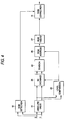
- Fig. 3 shows an arctangent circuit in which the three techniques are employed.
- the arctangent circuit as shown in Fig. 3 is used in place of the arctangent circuit in the digital FM demodulation circuit of Fig. 1.
- the first method is realized by the absolute value detection unit 11, the sign detection unit 12, and a sign correction unit 19.
- the absolute value detection unit 11 detects the absolute values of the input signals. Even when S/C is a negative value in the third quadrant of Fig. 2, S/C is processed as a positive value in the first quadrant, and a corresponding angle (arctangent) value is obtained from the ROM tables.
- the sign detection unit 12 detects the signs of the input signals.
- the sign correction unit 19 corrects the polarity of the obtained angle to be negative, so that the correct arctangent value is outputted. According to the above, the number of ROM tables 17 can be reduced.
- the output of the absolute value detection unit 11 is input to a level comparison unit 13 and a SC exchange unit 14.
- the level comparison unit 13 detects the level relationship between the input S and C signals.
- the SC exchange unit 14 only when the detection result of the level comparison unit 13 indicates S/C > 1, the values of S and C are exchanged with each other, and the exchanged values are then outputted.
- a ROM address unit 16 obtains an arctangent value corresponding to the exchanged value (C/S), from the ROM tables 17, and outputs the arctangent value.
- the S/C is processed as the S/C is exchanged with its inverse number C/S which is smaller than 1, and an angle (arctangent) corresponding to the inverse number from the ROM tables is obtained.
- the thus obtained value is corrected to the correct angle value on the basis of the expression (2) described in the second method.
- This process is performed by the exchange correction unit 18.
- the angle correction process is implemented.
- the signals which have passed through the SC exchange unit 14 are inputted to a division and roundoff unit 15.
- the division and roundoff unit 15 obtains S/C from the input S and C signals, and rounds off the obtained S/C to one of the typical values a0 to a7 which are uniformly divided as shown in the Table 4.
- arctangent values corresponding to the typical values are arranged in the ROM tables 17 with addresses.
- the ROM address unit 16 controls operations of reading out a corresponding arctangent value from the ROM tables 17 and outputting the read out arctangent value.
- the first embodiment described above is the most preferable embodiment which employs all the first to third methods so that the number of ROM tables can be reduced to a minimum level.
- an arctangent circuit which can prevent the S/N ratio from being degraded may be configured without employing the second method.
- a phase in the range of 0 to 90 degrees is used, and hence the graph of Fig. 2 cannot be equally divided in the direction of the S/C axis as described in the third technique. Therefore, there is studied typical values such as shown in Table 5 which are obtained on the basis of the typical values of Table 3.
- Fig. 4 shows an arctangent circuit which uses such typical values.
- the same components as those of Fig. 3 are denoted by the same reference numerals, and their detailed description is omitted.
- the phase in the range of 0 to 90 degrees is used.
- the SC exchange unit 14 and the exchange correction unit 18 which are used in the first embodiment are therefore unnecessary.
- the ROM address is determined in the following manner, and hence an exchange of S and C is required.
- the output of the absolute value detection unit 11 is supplied to the level comparison unit 23 and the SC exchange unit 24.
- the level comparison unit 23 detects the level relationship between the input S and C signals. Only when the detection result indicates S/C > 1, the values of S and C are exchanged with each other. The outputted values of S and C are divided in a division unit 25, so that S/C is obtained (when S/C > 1, the division is substantially performed as C/S). The division result is outputted.
- a ROM address unit 26 multiplies S/C by 7. At this time, an integer being one of from 0 to 7 is obtained as an integer part, and hence also a process of rounding the multiplication value to an integer value is implemented.
- S > C the arctangent of 45 to 90 degrees
- C/S is multiplied by 7, and the multiplication result is subtracted from 14. At this time, an integer being one of from 8 to 14 is obtained as an integer part, and hence also a process of rounding the subtraction value to an integer value is similarly implemented. As a result of the above processes, an integer one of from 0 to 14 is derived.
- ROM tables 27 hold arctangent values in one-to-one correspondence with such integers.
- a ROM address corresponding to the integer value obtained as a result of the above calculation is acquired in the ROM address unit 26.
- An arctangent value designated by the address is read out from the ROM tables 27, and then outputted.
- the number of the ROM tables is twice that in the first embodiment, the angle correction process which is performed in the first embodiment is not required. Furthermore, there appears no difference in S/N ratio of the demodulation output. Therefore, it is preferable to employ either of the embodiments in accordance with necessity.
- the number of ROM tables can be reduced while preventing the SN ratio from being impaired.
Abstract
Description
- The present invention relates to a digital FM demodulation circuit which uses an arctangent circuit having ROM tables.
- Fig. 1 is a schematic block diagram showing a conventional digital FM demodulation circuit. The digital FM demodulation circuit includes
delay circuits adders divider 4, and anarctangent circuit 5. The operation of the digital FM demodulation circuit will be described. In the demodulation circuit, there is inputted a digital FM signal into which an analog FM signal is converted with a sampling frequency that is four times higher than a frequency of the analog signal. - When the sampling frequency is set to be four times as large as the frequency of the original signal, it is possible to set a phase difference between the sampling frequency and an non-modulated digital FM signal at 90 degrees. Each time when a digital FM signal is passed through a delay circuit, the phase of the signal is delayed at 90 degrees. The sampled digital FM signal passes through a
delay circuit 1 to be converted to a second signal that is delayed for a constant time. The second signal is referred to as - On the other hand, the sampled digital FM signal is converted also to a third signal which is always phase-shifted at 90 degrees with respect to the second signal, by a Hilbert conversion circuit including the
delay circuits adder 3, and thedivider 4. The third signal is referred to asarctangent circuit 5. Thearctangent circuit 5 performs a division of the two signals to obtain - An output of the
arctangent circuit 5 is delayed for one sampling period by thedelay circuit 6, and then inverted by an inverting circuit which is not shown. The inverted output is supplied to one input of theadder 7. On the other hand, to the other input of theadder 7, the output of thearctangent circuit 5 is directly inputted. In theadder 7, the two inputs are added to each other, so that a FM detector output as a demodulated signal is obtained. - As described above, a general digital FM demodulation circuit requires an arctangent circuit in which the phase of a sampled signal is calculated from the amplitude of the signal. Usually, it is often that such a calculation circuit itself is not configured and the phase is obtained by using ROM tables corresponding to an input value.
- In most of A/D converter circuits, the output digital value is expressed by one bit in code information and n bits in amplitude information. In the following description, therefore, a 4-bit A/D converter in which code information consists of 1 bit and amplitude information of 3 bits is used as an example, and it is assumed that an analog FM signal is converted to a digital FM signal by the A/D converter and the digital FM signal is inputted to a digital FM demodulation circuit. In the 4-bit A/D converter, the amplitude of the input signal is expressed by one of digital values of 15 kinds from -7 to 7. Consequently, each of the above-mentioned S and C can have one of the values from -7 to 7, and 113 ROM tables of arctangents of S/C are necessary (when S/C ≥ 0, 64 ROM tables, and when S/C < 0, 49 ROM tables). When no countermeasure is taken, therefore, there arises a problem in that the cost of preparing ROM tables is too high.
- In view of the problem, it is an object of the invention to reduce the number of ROM tables used in an arctangent circuit without lowering the performance.
- According to the present invention, there is provided a digital FM demodulation circuit sampling an input analog FM signal and digitally detecting the sampled input signal, comprising:
- an arctangent circuit into which a second signal that is delayed from the sampled input signal for a constant time and a third signal that is different in phase at 90 degrees from the second signal are inputted, and which outputs a corresponding arctangent value based on a result of a division of the two input signals, and
- the arctangent circuit including:
- roundoff means for sequentially rounding the division result to one of a plurality of typical values; and
- ROM address unit for selecting an arctangent value corresponding to the rounded typical value from a ROM table containing typical arctangent values, and outputting the selected arctangent value.
-
- According to the present invention, the arctangent circuit may further comprise:
- polarity detection means for detecting whether the division result is a negative value; and
- a polarity correction unit which changes a polarity of
the outputted arctangent value, and
wherein if the polarity detection unit judges that the division result is a negative value, the polarity correction unit changes the polarity of the output arctangent value to negative. -
- According to the present invention, the arctangent circuit may further comprise:
- a level comparison unit comparing a level of the second signal with a level of the third signal;
- an exchange unit exchanging the second signal with the third signal; and
- a correction unit correcting the arctangent value,
wherein if the level comparison unit judges that the second signal is larger in level than the third signal, the exchange unit exchanges the second signal with the third signal, and selects a corresponding arctangent value from the ROM table based on the exchanged value, and the correction unit corrects the arctangent value outputted from the ROM table to the arctangent value to be obtained in the case where the second signal is not exchanged with the third signal. -
- In the drawings:
- Fig. 1 is a schematic block diagram of a digital FM demodulation circuit.
- Fig. 2 is a view showing relationships between S/C and its arctangent.
- Pig. 3 is a diagram showing an example of an arctangent circuit in the invention.
- Fig. 4 is a diagram showing another example of an arctangent circuit in the invention.
-
- Hereinafter, embodiments of the invention will be given with reference to the accompanying drawings. First, three techniques which are employed in the present invention will be described.
- Fig. 2 is a graph showing relationships between
- Table 1 shows values of S/C in the case where S and C may be one of 0 to 7 (3 bits).
7 ∞ 7 7/2 7/3 7/4 7/5 7/6 1 6 ∞ 6 3 2 3/2 6/5 1 6/7 5 ∞ 5 5/2 5/3 5/4 1 5/6 5/7 4 ∞ 4 2 4/3 1 4/5 2/3 4/7 3 ∞ 3 3/2 1 3/4 3/5 1/2 3/7 2 ∞ 2 1 2/3 1/2 2/5 1/3 2/7 1 ∞ 1 1/2 1/3 1/4 1/5 1/6 1/7 0 0 0 0 0 0 0 0 S C 0 1 2 3 4 5 6 7 - As shown in Table 1, S/C, and C/S in which S and C are exchanged with each other exist in a symmetrical relationship about the axis of
- From this expression, in the case where the arctangent is larger than 45 degrees in the case of S > C,
- From this expression, an angle in the case of S < C can be obtained by using an angle in the case of S > C.
- Therefore, the number of ROM tables can be reduced to about half of that in the case of Table 1.
- The applicant had an idea that the S/C axis of the graph of Fig. 2 is equally divided. When it is assumed that the above-described first technique is used, it is only required to consider the first quadrant of Fig. 2. As shown also in Table 1, infinite values exist in the range of S/C > 1. Therefore, the S/C axis cannot be equally divided. Therefore, it is assumed that also the above-described second technique is further used. In this case, it is only required to consider the range of the arctangent value from 0 to 45 degrees. In this range (0 ≤ S/C ≤ 1), therefore, the S/C axis can be equally divided.
- Table 2 below is a table where values of S/C which is not larger than 1 are arranged in ascending order.

- In Table 2, the column of "
- Next, on this principle, S/C = 1/7, 2/7, 3/7, 4/7, 5/7, 6/7, and 7/7 are extracted from Table 2 to produce Table 3 shown as follows.
S/C Phase difference from the previous phase (degree) 0 0 1/7 8.13 8.13 2/7 15.97 7.82 3/7 23.20 7.25 4/7 29.74 6.54 5/7 35.54 5.80 6/7 40.60 5.06 1 45.00 4.40 - As shown in Table 3, all the values of "phase difference from the previous phase" are equal to or less than 8.13 degrees. Even when the eight values of
- More specifically, as shown in Table. 4, when the S/C axis is equally divided at a0 to a7 and the corresponding eight values of
S/C 0 . a0 < 1/14 0 1/7-1/14 . a1 < 1/7+1/14 8.13 2/7-1/14 . a2 < 2/7+1/14 15.95 3/7-1/14 . a3 < 3/7+1/14 23.20 4/7-1/14 . a4 < 4/7+1/14 29.74 5/7-1/14 . a5 < 5/7+1/14 35.54 6/7-1/14 . a6 < 6/7+1/14 40.60 7/7-1/14 . a7 < 7/7 45.00 - When the above three techniques are employed, the number of ROM tables can be reduced to eight.
- Next, Fig. 3 shows an arctangent circuit in which the three techniques are employed. The arctangent circuit as shown in Fig. 3 is used in place of the arctangent circuit in the digital FM demodulation circuit of Fig. 1.
- First, inputted S and C signals are inputted into an absolute
value detection unit 11 and asign detection unit 12. The first method is realized by the absolutevalue detection unit 11, thesign detection unit 12, and asign correction unit 19. The absolutevalue detection unit 11 detects the absolute values of the input signals. Even when S/C is a negative value in the third quadrant of Fig. 2, S/C is processed as a positive value in the first quadrant, and a corresponding angle (arctangent) value is obtained from the ROM tables. On the other hand, thesign detection unit 12 detects the signs of the input signals. When S/C is a negative value, thesign correction unit 19 corrects the polarity of the obtained angle to be negative, so that the correct arctangent value is outputted. According to the above, the number of ROM tables 17 can be reduced. - The output of the absolute
value detection unit 11 is input to alevel comparison unit 13 and aSC exchange unit 14. Thelevel comparison unit 13, theSC exchange unit 14, and anexchange correction unit 18 which corrects the phase value realize the second method. Thelevel comparison unit 13 detects the level relationship between the input S and C signals. In theSC exchange unit 14, only when the detection result of thelevel comparison unit 13 indicates S/C > 1, the values of S and C are exchanged with each other, and the exchanged values are then outputted. AROM address unit 16 obtains an arctangent value corresponding to the exchanged value (C/S), from the ROM tables 17, and outputs the arctangent value. - Specifically, when the S/C is larger than 1, the S/C is processed as the S/C is exchanged with its inverse number C/S which is smaller than 1, and an angle (arctangent) corresponding to the inverse number from the ROM tables is obtained. The thus obtained value is corrected to the correct angle value on the basis of the expression (2) described in the second method. This process is performed by the
exchange correction unit 18. When S/C is larger than 1, the angle correction process is implemented. - The signals which have passed through the
SC exchange unit 14 are inputted to a division androundoff unit 15. According to this configuration, the third method is realized. The division androundoff unit 15 obtains S/C from the input S and C signals, and rounds off the obtained S/C to one of the typical values a0 to a7 which are uniformly divided as shown in the Table 4. For the typical values a0 to a7, arctangent values corresponding to the typical values are arranged in the ROM tables 17 with addresses. TheROM address unit 16 controls operations of reading out a corresponding arctangent value from the ROM tables 17 and outputting the read out arctangent value. - The first embodiment described above is the most preferable embodiment which employs all the first to third methods so that the number of ROM tables can be reduced to a minimum level. Alternatively, an arctangent circuit which can prevent the S/N ratio from being degraded may be configured without employing the second method. In this case, a phase in the range of 0 to 90 degrees is used, and hence the graph of Fig. 2 cannot be equally divided in the direction of the S/C axis as described in the third technique. Therefore, there is studied typical values such as shown in Table 5 which are obtained on the basis of the typical values of Table 3.
S/C (S/C)×7 0 0 0 1/7 1 8.13 8.13 2/7 2 15.95 7.82 3/7 3 23.20 7.25 4/7 4 29.74 6.54 5/7 5 35.54 5.80 6/7 6 40.60 5.06 7/7 7 45.00 4.40 S/C 14-(C/S)×7 7/6 8 49.40 4.40 7/5 9 54.46 5.06 7/4 10 60.26 5.80 7/3 11 66.80 6.54 7/2 12 74.05 7.25 7/1 13 81.87 7.82 7/0 14 90.00 8.13 - As shown in the column of "phase difference from the previous phase" of Table 5, the maximum value of "phase difference from the previous phase" is identical with that in the first embodiment. Even when an arctangent circuit is configured by using only these typical values, therefore, a large difference does not arise in the SN ratio of the detector output.
- Fig. 4 shows an arctangent circuit which uses such typical values. The same components as those of Fig. 3 are denoted by the same reference numerals, and their detailed description is omitted. In the second embodiment, the phase in the range of 0 to 90 degrees is used. In principle, the
SC exchange unit 14 and theexchange correction unit 18 which are used in the first embodiment are therefore unnecessary. In the second embodiment, however, the ROM address is determined in the following manner, and hence an exchange of S and C is required. - In the second embodiment, the output of the absolute
value detection unit 11 is supplied to thelevel comparison unit 23 and theSC exchange unit 24. Thelevel comparison unit 23 detects the level relationship between the input S and C signals. Only when the detection result indicates S/C > 1, the values of S and C are exchanged with each other. The outputted values of S and C are divided in adivision unit 25, so that S/C is obtained (when S/C > 1, the division is substantially performed as C/S). The division result is outputted. - In the case where S ≤ C (the arctangent is 0 to 45 degrees), a
ROM address unit 26 multiplies S/C by 7. At this time, an integer being one of from 0 to 7 is obtained as an integer part, and hence also a process of rounding the multiplication value to an integer value is implemented. In the case of S > C (the arctangent of 45 to 90 degrees), C/S is multiplied by 7, and the multiplication result is subtracted from 14. At this time, an integer being one of from 8 to 14 is obtained as an integer part, and hence also a process of rounding the subtraction value to an integer value is similarly implemented. As a result of the above processes, an integer one of from 0 to 14 is derived. - ROM tables 27 hold arctangent values in one-to-one correspondence with such integers. A ROM address corresponding to the integer value obtained as a result of the above calculation is acquired in the
ROM address unit 26. An arctangent value designated by the address is read out from the ROM tables 27, and then outputted. - In the second embodiment, although the number of the ROM tables is twice that in the first embodiment, the angle correction process which is performed in the first embodiment is not required. Furthermore, there appears no difference in S/N ratio of the demodulation output. Therefore, it is preferable to employ either of the embodiments in accordance with necessity.
- As described above, according to the invention, the number of ROM tables can be reduced while preventing the SN ratio from being impaired.
Claims (3)
- A digital FM demodulation circuit sampling an input analog FM signal and digitally detecting the sampled input signal, comprising:an arctangent circuit into which a second signal that is delayed from the sampled input signal for a constant time and a third signal that is different in phase at 90 degrees from the second signal are inputted, and which outputs a corresponding arctangent value based on a result of a division of the two input signals, andsaid arctangent circuit including:roundoff means for sequentially rounding the division result to one of a plurality of typical values; andROM address unit for selecting an arctangent value corresponding to the rounded typical value from a ROM table containing typical arctangent values, and outputting the selected arctangent value.
- A digital FM demodulation circuit according to claim 1, wherein said arctangent circuit further comprising:polarity detection means for detecting whether the division result is a negative value; anda polarity correction unit which changes a polarity of the outputted arctangent value, and
wherein if said polarity detection unit judges that the division result is a negative value, said polarity correction unit changes the polarity of the output arctangent value to negative. - A digital FM demodulation circuit according to claim 2, wherein said arctangent circuit further comprising:a level comparison unit comparing a level of the second signal with a level of the third signal;an exchange unit exchanging the second signal with the third signal; anda correction unit correcting the arctangent value,
wherein if said level comparison unit judges that the second signal is larger in level than the third signal, said exchange unit exchanges the second signal with the third signal, and selects a corresponding arctangent value from said ROM table based on the exchanged value, and said correction unit corrects the arctangent value outputted from said ROM table to the arctangent value to be obtained in the case where the second signal is not exchanged with the third signal.
Applications Claiming Priority (2)
| Application Number | Priority Date | Filing Date | Title |
|---|---|---|---|
| JP6626198 | 1998-03-02 | ||
| JP06626198A JP4294114B2 (en) | 1998-03-02 | 1998-03-02 | Digital FM detection circuit |
Publications (2)
| Publication Number | Publication Date |
|---|---|
| EP0940909A1 true EP0940909A1 (en) | 1999-09-08 |
| EP0940909B1 EP0940909B1 (en) | 2005-04-13 |
Family
ID=13310748
Family Applications (1)
| Application Number | Title | Priority Date | Filing Date |
|---|---|---|---|
| EP99301461A Expired - Lifetime EP0940909B1 (en) | 1998-03-02 | 1999-02-26 | Digital FM demodulation circuit |
Country Status (4)
| Country | Link |
|---|---|
| US (1) | US6229386B1 (en) |
| EP (1) | EP0940909B1 (en) |
| JP (1) | JP4294114B2 (en) |
| DE (1) | DE69924660T2 (en) |
Cited By (4)
| Publication number | Priority date | Publication date | Assignee | Title |
|---|---|---|---|---|
| FR2815195A1 (en) * | 2000-10-05 | 2002-04-12 | Mitsubishi Electric Corp | DIGITAL FM DEMODULATOR AND IMAGE SIGNAL PROCESSOR USING SUCH A DEMODULATOR |
| WO2006099532A2 (en) * | 2005-03-11 | 2006-09-21 | Qualcomm Incorporated | Automatic frequency control for a wireless communication system with multiple subcarriers |
| EP1811676A1 (en) * | 2004-11-05 | 2007-07-25 | Pioneer Corporation | Fm receiver |
| US8401503B2 (en) | 2005-03-01 | 2013-03-19 | Qualcomm Incorporated | Dual-loop automatic frequency control for wireless communication |
Families Citing this family (2)
| Publication number | Priority date | Publication date | Assignee | Title |
|---|---|---|---|---|
| US20020101939A1 (en) * | 2000-11-09 | 2002-08-01 | Sundaresan Harini V. | Fixed-point DSP implementation of FM demodulation and decoding |
| TW200915096A (en) * | 2007-09-27 | 2009-04-01 | Alcor Micro Corp | Angle computation method and related circuit |
Citations (5)
| Publication number | Priority date | Publication date | Assignee | Title |
|---|---|---|---|---|
| GB2113930A (en) * | 1982-01-26 | 1983-08-10 | Plessey Co Plc | Frequency discriminator |
| US4470147A (en) * | 1981-09-15 | 1984-09-04 | International Standard Electric Corporation | Radio receiver with quadrature demodulation and digital processing |
| US4560941A (en) * | 1984-09-21 | 1985-12-24 | General Electric Company | Frequency modulation detector using digital signal vector processing |
| US4875017A (en) * | 1987-12-08 | 1989-10-17 | Kabushiki Kaisha Toshiba | Digital FM demodulating apparatus |
| EP0526747A2 (en) * | 1991-07-11 | 1993-02-10 | Honeywell Inc. | Transcendental function approximation apparatus and method |
Family Cites Families (1)
| Publication number | Priority date | Publication date | Assignee | Title |
|---|---|---|---|---|
| US5848739A (en) * | 1997-01-17 | 1998-12-15 | Package Research, Inc. | Pump dispenser for flowable materials |
-
1998
- 1998-03-02 JP JP06626198A patent/JP4294114B2/en not_active Expired - Fee Related
-
1999
- 1999-02-26 US US09/258,137 patent/US6229386B1/en not_active Expired - Lifetime
- 1999-02-26 EP EP99301461A patent/EP0940909B1/en not_active Expired - Lifetime
- 1999-02-26 DE DE69924660T patent/DE69924660T2/en not_active Expired - Lifetime
Patent Citations (5)
| Publication number | Priority date | Publication date | Assignee | Title |
|---|---|---|---|---|
| US4470147A (en) * | 1981-09-15 | 1984-09-04 | International Standard Electric Corporation | Radio receiver with quadrature demodulation and digital processing |
| GB2113930A (en) * | 1982-01-26 | 1983-08-10 | Plessey Co Plc | Frequency discriminator |
| US4560941A (en) * | 1984-09-21 | 1985-12-24 | General Electric Company | Frequency modulation detector using digital signal vector processing |
| US4875017A (en) * | 1987-12-08 | 1989-10-17 | Kabushiki Kaisha Toshiba | Digital FM demodulating apparatus |
| EP0526747A2 (en) * | 1991-07-11 | 1993-02-10 | Honeywell Inc. | Transcendental function approximation apparatus and method |
Cited By (8)
| Publication number | Priority date | Publication date | Assignee | Title |
|---|---|---|---|---|
| FR2815195A1 (en) * | 2000-10-05 | 2002-04-12 | Mitsubishi Electric Corp | DIGITAL FM DEMODULATOR AND IMAGE SIGNAL PROCESSOR USING SUCH A DEMODULATOR |
| EP1811676A1 (en) * | 2004-11-05 | 2007-07-25 | Pioneer Corporation | Fm receiver |
| EP1811676A4 (en) * | 2004-11-05 | 2010-08-11 | Pioneer Corp | Fm receiver |
| US8401503B2 (en) | 2005-03-01 | 2013-03-19 | Qualcomm Incorporated | Dual-loop automatic frequency control for wireless communication |
| WO2006099532A2 (en) * | 2005-03-11 | 2006-09-21 | Qualcomm Incorporated | Automatic frequency control for a wireless communication system with multiple subcarriers |
| WO2006099532A3 (en) * | 2005-03-11 | 2008-07-24 | Qualcomm Inc | Automatic frequency control for a wireless communication system with multiple subcarriers |
| US8009775B2 (en) | 2005-03-11 | 2011-08-30 | Qualcomm Incorporated | Automatic frequency control for a wireless communication system with multiple subcarriers |
| CN101313546B (en) * | 2005-03-11 | 2013-01-16 | 高通股份有限公司 | Method and device for automatic frequency control for a wireless communication system with multiple subcarriers |
Also Published As
| Publication number | Publication date |
|---|---|
| DE69924660T2 (en) | 2005-09-29 |
| JP4294114B2 (en) | 2009-07-08 |
| US6229386B1 (en) | 2001-05-08 |
| DE69924660D1 (en) | 2005-05-19 |
| EP0940909B1 (en) | 2005-04-13 |
| JPH11251841A (en) | 1999-09-17 |
Similar Documents
| Publication | Publication Date | Title |
|---|---|---|
| EP0180969B1 (en) | Automatic level control circuit for an ad converter | |
| US6222477B1 (en) | Cascade A/D converter | |
| US5761251A (en) | Dual automatic gain control and DC offset correction circuit for QAM demodulation | |
| EP0692895B1 (en) | Demodulator using differential detection | |
| EP0078687B1 (en) | Analog to digital converter | |
| EP0396746B1 (en) | Picture receiver controller | |
| EP0875735A1 (en) | Interpolation circuit for an incremental encoder | |
| EP0940909B1 (en) | Digital FM demodulation circuit | |
| EP0877489A2 (en) | Direct resolver to digital converter | |
| US6359942B1 (en) | FSK demodulator | |
| US4768015A (en) | A/D converter for video signal | |
| EP0932027B1 (en) | Offset correcting circuit for encoder | |
| US6018552A (en) | Differential detection receiver | |
| EP0391643B1 (en) | Digital signal clamp circuitry | |
| US4528511A (en) | Circuit for digital FM demodulation | |
| EP0177069B1 (en) | Arrangement for combining the output signals from a plurality of transmitters tuned to the same frequency | |
| US6393067B1 (en) | Differential detection receiver | |
| US6028475A (en) | Method and apparatus for demodulating multi-level QAM signal | |
| EP0689340B1 (en) | Signal-processing circuit | |
| JPH0456511B2 (en) | ||
| EP0702290B1 (en) | Digital dividing apparatus using a look-up table | |
| US6127956A (en) | Post-conversion system for an analog-to-digital converter which sets an added bit of resolution if an intermediate sample is within a threshold | |
| US4875044A (en) | Digital limiting circuit | |
| JPH05276036A (en) | Offset compensation circuit for a/d converter | |
| JP3387165B2 (en) | Clamp potential correction circuit |
Legal Events
| Date | Code | Title | Description |
|---|---|---|---|
| PUAI | Public reference made under article 153(3) epc to a published international application that has entered the european phase |
Free format text: ORIGINAL CODE: 0009012 |
|
| AK | Designated contracting states |
Kind code of ref document: A1 Designated state(s): DE FR GB |
|
| AX | Request for extension of the european patent |
Free format text: AL;LT;LV;MK;RO;SI |
|
| 17P | Request for examination filed |
Effective date: 20000216 |
|
| AKX | Designation fees paid |
Free format text: DE FR GB |
|
| 17Q | First examination report despatched |
Effective date: 20030526 |
|
| GRAP | Despatch of communication of intention to grant a patent |
Free format text: ORIGINAL CODE: EPIDOSNIGR1 |
|
| GRAS | Grant fee paid |
Free format text: ORIGINAL CODE: EPIDOSNIGR3 |
|
| GRAA | (expected) grant |
Free format text: ORIGINAL CODE: 0009210 |
|
| AK | Designated contracting states |
Kind code of ref document: B1 Designated state(s): DE FR GB |
|
| REG | Reference to a national code |
Ref country code: GB Ref legal event code: FG4D |
|
| REF | Corresponds to: |
Ref document number: 69924660 Country of ref document: DE Date of ref document: 20050519 Kind code of ref document: P |
|
| PLBE | No opposition filed within time limit |
Free format text: ORIGINAL CODE: 0009261 |
|
| STAA | Information on the status of an ep patent application or granted ep patent |
Free format text: STATUS: NO OPPOSITION FILED WITHIN TIME LIMIT |
|
| ET | Fr: translation filed | ||
| 26N | No opposition filed |
Effective date: 20060116 |
|
| PGFP | Annual fee paid to national office [announced via postgrant information from national office to epo] |
Ref country code: FR Payment date: 20120221 Year of fee payment: 14 |
|
| PGFP | Annual fee paid to national office [announced via postgrant information from national office to epo] |
Ref country code: DE Payment date: 20120222 Year of fee payment: 14 |
|
| PGFP | Annual fee paid to national office [announced via postgrant information from national office to epo] |
Ref country code: GB Payment date: 20120222 Year of fee payment: 14 |
|
| GBPC | Gb: european patent ceased through non-payment of renewal fee |
Effective date: 20130226 |
|
| REG | Reference to a national code |
Ref country code: FR Ref legal event code: ST Effective date: 20131031 |
|
| REG | Reference to a national code |
Ref country code: DE Ref legal event code: R119 Ref document number: 69924660 Country of ref document: DE Effective date: 20130903 |
|
| PG25 | Lapsed in a contracting state [announced via postgrant information from national office to epo] |
Ref country code: DE Free format text: LAPSE BECAUSE OF NON-PAYMENT OF DUE FEES Effective date: 20130903 Ref country code: FR Free format text: LAPSE BECAUSE OF NON-PAYMENT OF DUE FEES Effective date: 20130228 Ref country code: GB Free format text: LAPSE BECAUSE OF NON-PAYMENT OF DUE FEES Effective date: 20130226 |