BACKGROUND OF THE INVENTION
1. FIELD OF THE INVENTION
This invention relates generally to a magnetic
sensor, and more particularly to a magnetic head and a
magnetic memory used for computers and information
processing units.
2. DESCRIPTION OF THE RELATED ART
Magnetic recording media have been predominantly
magnetic disks and magnetic tapes. They are manufactured
by forming a thin magnetic film on an Al substrate or a
resin tape. A magnetic head utilizing an electromagnetic
conversion operation is used in order to write and read
magnetic information to and from these magnetic media.
This magnetic head comprises a write portion for writing
the magnetic information to the recording medium and a read
portion for reading out the magnetic information from the
recording medium. A so-called "induction type head", which
comprises a coil and magnetic poles that wrap the coil from
above and below and are electrically connected to the coil,
is generally used for the write portion. Magneto-resistance
effect (MR) heads have been proposed recently
for the read portion so as to cope with the magnetic
information having a high recording density. Among the MR
heads, those heads which utilize the gigantic magneto-resistance
effect (GMR) are well known nowadays.
Recently, a magnetic sensor using a ferromagnetic
tunnel magneto-resistance effect (spin tunnel magneto-resistance
effect: TMR) has been proposed for a magnetic
memory as described in JP-A-10-4227. This TMR can obtain a
greater resistance change ratio by causing a current to
flow in a direction of film thickness of the magneto-resistance
effect film than the conventional magneto-resistance
effect devices such as the GMRs which cause a
current to flow in a direction of the main plane of the
magneto-resistance effect film.
According to the construction described in JP-A-10-4227,
however, an upper electrode stack 30 comprising at
least a free ferromagnetic layer 32 and a protective layer
34 must be formed inside a contact hole defined in an
insulating layer 40. Therefore, production is difficult,
and film quality and film thickness of each layer inside
the contact hole are likely to fluctuate from a desired
level.
SUMMARY OF THE INVENTION
In view of the problems described above, the
present invention aims at providing a construction of a
magnetic sensor using a spin tunnel magneto-resistance
effect (TMR) which construction can be manufactured more
easily than the prior art devices and can stably keep film
quality and thickness at a desired level, and a method of
producing the magnetic sensor.
To accomplish the object, a spin tunnel magneto-resistance
effect magnetic sensor according to the present
invention comprises a first insulating film which allows a
current to tunnel and flow therethrough, a first magnetic
layer formed on a first surface of the first insulating
film and containing a ferromagnetic substance, a second
magnetic layer formed on a second surface of the first
insulating film and containing a ferromagnetic substance, a
third magnetic layer formed on the second magnetic layer
and containing an anti-ferromagnetic substance for fixing
magnetization of the second magnetic layer, a second
insulating film formed on at least one of the first and
third magnetic layers and having an opening in a predetermined
region, a first electrode electrically connected to
one of the first and third magnetic layers only inside the
opening of the second insulating film, and a second
electrode for causing a current to flow between at least
one of the first and second magnetic layer and the first
electrode through the first insulating film.
A method of producing a spin tunnel magneto-resistance
effect type magnetic sensor having a first
magnetic layer containing a ferromagnetic substance, a
second magnetic layer containing a ferromagnetic substance
and a third magnetic layer containing an anti-ferromagnetic
substance for fixing magnetization of the second magnetic
layer according to the present invention comprises the
steps of (a) forming the third magnetic layer over a
substrate by sputtering, (b) forming the second magnetic
layer on the third magnetic layer by sputtering, (c)
processing at least the second and third magnetic layers
into a first pattern, (d) forming a first insulating film,
which allows an electric current to tunnel and flow there-through,
on at least the first pattern, by sputtering, (e)
forming a first magnetic layer on the first insulating film
by sputtering, (f) processing at least the first magnetic
layer and the first insulating film into a second pattern,
(g) forming a second insulating film in at least a
predetermined region of the second pattern, (h) forming an
opening in a predetermined region of the second insulating
film and (i) forming a first electrode, which is
electrically connected to the first magnetic layer only
inside the opening of the second insulating film, and
forming a second electrode electrically connected to the
second magnetic layer.
BRIEF DESCRIPTION OF THE DRAWINGS
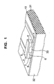
Fig. 1 is a perspective view showing a magnetic
head according to a first embodiment of the present
invention;
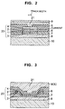
Fig. 2 is a sectional view showing a part of the
magnetic head according to the first embodiment of the
present invention;
Fig. 3 is a sectional view showing a part of a
magnetic head according to a second embodiment of the
present invention;
Fig. 4 is a sectional view showing a part of a
magnetic head according to a third embodiment of the
present invention;
Fig. 5 is a sectional view showing a part of a
magnetic head according to a fourth embodiment of the
present invention;
Fig. 6 is a sectional view showing a part of a
magnetic head according to a fifth embodiment of the
present invention;
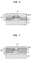
Fig. 7 is a sectional view showing a part of a
magnetic head according to a sixth embodiment of the
present invention;
Fig. 8 is a sectional view showing a part of a
magnetic head according to a seventh embodiment of the
present invention;
Fig. 9 is a sectional view showing a part of a
magnetic head according to an eighth embodiment of the
present invention;
Fig. 10 is a perspective view showing a magnetic
recording/reproducing apparatus using the magnetic head
according to the embodiments of the present invention;
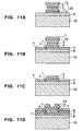
Figs. 11A to 11G are sectional views each showing
a production step of the magnetic head shown in Fig. 4;
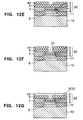
Figs. 12A to 12G are sectional views each showing
a production step of the magnetic head shown in Fig. 8;
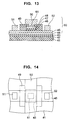
Fig. 13 is a sectional view showing a magnetic
memory according to one embodiment of the present
invention; and
Fig. 14 is a plan view showing the magnetic
memory according to one embodiment of the present
invention.
DETAILED DESCRIPTION OF THE EMBODIMENTS
Several embodiments of the present invention,
wherein a magnetic sensor according to the present
invention is applied to a reproducing magnetic head, will
be explained initially.
The recording/reproducing head used in the first
embodiment includes a reproducing TMR head utilizing a TMR
(spin tunnel magneto-resistance effect) and an induction
type recording thin film magnetic head. The reproducing
TMR head is mounted onto a substrate, and the recording
thin film magnetic head is mounted onto the TMR head.
This embodiment employs the construction for
preventing a current flowing through a magneto-resistance
effect film of the reproducing TMR head from leaking to a
magnetic domain control layer, and improves detection
efficiency of a resistance change ratio of the magneto-resistance
effect film. Also, this embodiment reduces the
width of the region, in which the current of the magneto-resistance
effect film flows, by reducing the width of
electrodes which are in contact with the magneto-resistance
effect film, and reduces a track width, too. In this way,
this embodiment provides a reproducing TMR head capable of
coping with a magnetic recording medium having a higher
recording density.
The construction of the reproducing TMR head
according to the first embodiment will be explained more
concretely with reference to Figs. 1 and 2. The recording
thin film magnetic head is disposed in superposition with
the reproducing TMR head. The explanation of the construction
of this thin film magnetic head will be omitted hereby
because it is well known in the art.
A lower shield film 10 is formed on a ceramic
substrate 31 as shown in Fig. 1. An electrode film 8
patterned into a desired shape is disposed on the lower
shield film 10. A magneto-resistance effect film 20 having
a four-layered structure is disposed on and at a part of
the electrode film 8. Magnetic domain control films 7 are
arranged on both sides of the magneto-resistance effect
film 20 and an insulating film 6 is disposed on the
magneto-resistance effect film 20 and the magnetic domain
control films 7 in such a fashion as to bury them. As
shown in Fig. 2 which is a sectional view taken along a
line A - A' of Fig. 1, a through-hole (opening) 21 is bored
in the insulating film 6 at a position which is situated on
the magneto-resistance effect film 20. An electrode film 5
is arranged on the insulating film 6 and keeps contact with
the magneto-resistance effect film 20 at only the through-hole
portion 21. Therefore, when a current is caused to
flow from the electrode film 5 to the electrode film 8,
this current flows from the portion, at which the electrode
film 5 is in contact with the magneto-resistance effect
film 20, to the magneto-resistance effect film 20 in the
direction of film thickness. Consequently, the width of
the region of the magneto-resistance effect film 20, in
which the current flows, is limited substantially to the
width of the through-hole 21 and this width practically
serves as a track width. Incidentally, an upper shield
film 9 (not shown in Fig. 1) is disposed on the electrode
film 5. The shield films 9 and 10 are disposed in order to
magnetically shield a leakage flux from the recording
medium and to improve spatial resolution of the reproducing
head.
The magneto-resistance effect film 20 has the
four-layered structure comprising a ferromagnetic free
layer 3, an electrical insulating layer 1, a ferromagnetic
fixing layer 2 and an anti-ferromagnetic layer 4 that are
laminated in order named. The free layer 3 and the fixing
layer 2 are formed in such a fashion that their axes of
easy magnetization are parallel. Magnetization of the
fixing layer 2 is fixed to a predetermined direction due to
its magnetic exchange/coupling with the anti-ferromagnetic
film 4. When the reproducing TMR head opposes the magnetic
recording medium, magnetization of the free layer 3 rotates
in accordance with the direction of magnetization of the
magnetic information recorded on the magnetic recording
medium. Therefore, the direction of magnetization of the
free layer 3 is parallel, or anti-parallel, to the
direction of magnetization of the fixing layer 2. When the
current is caused to flow through the magneto-resistance
effect film 20 in the direction of film thickness through
the electrode films 5 and 8, the current flows while
tunneling through the insulating film 1. The electric
resistance of the magneto-resistance effect film 20 changes
depending on whether the directions of magnetization of the
free layer 3 and the fixing layer 2 are parallel or anti-parallel
to each other, due to the spin tunnel magneto-resistance
effect (TMR). In other words, the tunnel
current changes depending on the relative direction of the
spin of magnetization in the free layer 3 and in the fixing
layer 2. The recorded signal can be reproduced by detecting
this change.
The magnetic domain control film 7 is a ferromagnetic
film for applying a bias magnetic field to the
free layer 3 in order to restrict the occurrence of the
magnetic domain of the free layer 3. This embodiment
employs the positional relationship such that the upper
surface of each magnetic domain control film 7 is always
positioned below the upper surface of the insulating layer
1 (on the side of the substrate 31 shown in Fig. 1) and
that the fixing layer 2 and each magnetic domain control
film 7 are out of mutual contact. Because the magnetic
domain control film 7 has a low resistivity, a part of the
current flowing from the electrode film 5 to the electrode
film 8 will leak from the fixing layer 2 to the electrode
film 8 through the magnetic domain control film 7 without
tunneling through the insulating film 1 if the magnetic
domain control film 7 keeps contact with the fixing layer
2. The construction shown in Fig. 2 can prevent the leak
of the current because the fixing layer 2 and the magnetic
domain control films 7 are out of mutual contact.
Next, the material of each part will be
explained. The lower shield film 10 is made of Co type
amorphous alloys such as CoNbZr, NiFe alloys, FeAlSi alloys
or CoNiFe alloys. The film thickness is from 1 to 5 µm.
The upper shield film 9 is made of NiFe alloys or CoNiFe
alloys and the absolute value of its magneto-restriction
constant is not greater than 5 × 10⁻⁶. The upper shield
film 9 can be used also as the lower core of the recording
thin film magnetic head and in this case, the upper shield
film 9 may be a multi-layered film comprising a ferromagnetic
layer and an oxide, or a ferromagnetic alloy film
that contains a metalloid such as B or P. In addition, the
upper shield film 9 preferably has a high resistivity (at
least 40 µΩ · cm) so as to improve high frequency
characteristics of the recording thin film magnetic head.
Since the electrode film 8 serves as the base
film of the magneto-resistance effect film 20, it must be
an electrode film which stabilizes the characteristics of
the magneto-resistance effect film 20 and provides a high
resistance change amount. More concretely, the surface of
the electrode film 8 is preferably flat and clean and when
a high current density is taken into consideration, the
electrode film 8 is preferably made of a material having a
high melting point. Therefore, the electrode film 8 is
formed by sputtering or vacuum deposition of those
elements, as low resistivity materials, which have a high
melting point but exhibit low exothermy, such as Ta, Nb,
Ru, Mo, Pt, Ir, etc, alloys containing these elements, such
as Ta alloys, TaW alloys, or alloys of W, Cu, Al, and so
forth. The thickness of the electrode film 8 is from 3 to
30 nm and is changed in accordance with the spacing between
the shield film 10 and the shield film 9. The smaller the
thickness of the electrode film 8, the smaller becomes the
spacing between the shield film 10 and the shield film 9,
and the higher becomes resolution of the reproducing TMR
head. This electrode film 8 may be a multi-layered film
(e.g. a multi-layered structure of Ta layer/Pt layer/Ta
layer or Ta layer/Cu layer/Ta layer).
The electrode film 5 may be made of the same
material as that of the electrode film 8.
The free layer 3 of the magneto-resistance effect
film 20 may have a single layered structure made of a
ferromagnetic material such as a NiFe alloy, a Co alloy, a
FeCo alloy or a CoNiFe alloy, or a multi-layered structure
containing a ferromagnetic layer for preventing diffusion
on the interface or restricting anisotropic dispersion.
Examples of the multi-layered structure include a structure
of Co layer/NiFe layer/Co layer and a multi-layered structure
of a Co layer/NiFe alloy layer/CoFe layer. Which
material is used for the free layer 3 and whether the free
layer 3 uses the single layer structure or the multi-layered
structure are determined also by the combination
with the electrode film 8 as the base. The fixing layer 2
can be made of Co or a Co alloy, or may be made of the same
material or may have the same structure, as that of the
free layer 3. The fixing layer 2 may also comprise a
multi-layered structure of a magnetic layer(s) and a
nonmagnetic layer(s). For example, it may comprise a
multi-layered structure of ferromagnetic layer/nonmagnetic
layer/Co layer such as Co layer/Ru layer/Co layer. The
anti-ferromagnetic layer 4 may be made of IrMn, CrMn type
alloys (such as CrMnPt, CrMnRu and CrMnRh), MnRh alloys,
MnPt alloys, MnPtPd alloys, NiMn alloys, NiMnPd alloys,
MnRhRu alloys, NiO, CoO alloys, Fe2O3 and Fe3O4 alloys and a
CrAl alloy. Alternatively, the anti-ferromagnetic film 4
may comprise a multi-layered film made of the combination
of these materials. The film thickness is 3 to 10 nm for
the free layer 3, 1 to 10 nm for the fixing layer 2 and 2
to 25 nm for the anti-ferromagnetic film 4. These films
can be formed by sputtering.
The insulating layer 1 of the magneto-resistance
effect film 20 is made of any of an oxide, a nitride, a
fluoride and a boride, or a material containing any of
them. For example, it is made of Al2O3, SiO2, Ta2O5, TiO2 or
an oxide having a perovskite structure, or a mixed phase of
any of these oxides, to which nitrogen is partly added, and
a nitride. The insulating layer 1 may be a multi-layered
film. The thickness of the insulating layer 1 is extremely
small, for example, 0.2 to 3 nm.
On the other hand, the insulating film 6 is made
of Al2O3 or SiO2. An insulating film having a high
dielectric withstand voltage can be obtained by employing a
multi-layered structure of a non-magnetic metal film/oxide
film/non-magnetic metal film or a ferromagnetic metal
film/oxide film/ferromagnetic metal film. For example, the
insulating film 6 may have a multi-layered structure of an
Al film/Al2O3 film/Al film and a multi-layered structure of
a Ni film/NiO film/Ni film or a Co film/CoO film/Co film.
The insulating film 6 can be made of an oxide containing at
least one of Ti, Sr and Ba. Among them, the film containing
Ti, Sr or Ba becomes a film containing the perovskite
structure and can improve the dielectric withstand voltage.
The magnetic domain control film 7 comprises a Co
type hard ferromagnetic film. A film of Cr, Nb or Ta as a
non-magnetic metal may be disposed as the base of the
magnetic domain control film 7.
Incidentally, the width of the through-hole 21 of
the insulating film 21 is preferably as small as possible
because it determines the track width. The production
process for this purpose may be as follows, for example.
The lower shield film 10 and the magneto-resistance effect
film 20 are formed first on the substrate 31. After the
magneto-resistance effect film 20 is etched by milling
method, the magnetic domain control films 7 are then
formed. The magnetic domain control films 7 formed on the
magneto-resistance effect film 20 are removed by lift-off.
The insulating film 6 is formed. It is formed by sputtering
or CVD. Next, this insulating film 6 is etched by RIE
(Reactive Ion Etching) and the through-hole 21 is formed.
The etching condition at this time is of importance.
Namely, a CHF3 or chlorine gas is used for etching so that
the width of the through-hole 21 becomes small. After the
electrode film 5 is formed, the through-hole 21 is filled
with this electrode film 5. The surface of the electrode
film 5 is processed into a flat surface by etching or CMP
(Chemical Mechanical Polishing) and the upper shield film 9
is formed by sputtering or plating on this flat electrode
film 5. Thereafter, the recording thin film magnetic head
is formed on the upper shield film 9.
Next, the explanation will be given on the
reproducing operation of the magnetic information of the
recording medium by using the reproducing TMR head having
the construction shown in Figs. 1 and 2. First, the float-up
surface 32 of the magneto-resistance effect head is
caused to float above the recording medium so that the
float-up surface 32 and the recording medium oppose each
other with a small spacing between them. The direction of
magnetization of the fixing layer 2 does not change because
it is fixed by magnetic exchange/coupling with the anti-ferromagnetic
film 4. On the other hand, magnetization of
the free layer 3 rotates with the direction of magnetization
of the magnetic information of the recording medium.
In consequence, the direction of magnetization of the
fixing layer 2 and the direction of magnetization of the
free layer 2 are either parallel or anti-parallel to each
other depending on the magnetic information of the recording
medium. When the current is caused to flow between the
electrode films 5 and 8, the current flows in the direction
of film thickness while tunneling through the insulating
layer 1 of the magneto-resistance effect film 20. The
electric resistance of the magneto-resistance effect film
20 at this time varies depending on whether the direction
of magnetization of the fixing layer 2 and that of the free
layer 3 are parallel or anti-parallel, due to the spin
tunnel magneto-resistance effect. This means that the
magnetic information of the recording medium can be
reproduced by detecting the current between the electrode
films 5 and 8 and by detecting the resistance change ratio.
Incidentally, when the magnetic information is recorded to
the recording medium, the information is recorded by the
recording thin film magnetic head mounted onto the
reproducing TMR head by floating the float-up surface 32
over the recording medium.
In the reproducing TMR head of the first embodiment
described above, the width of the electrode film 5,
which is in contact with the magneto-resistance effect film
20, is decreased by the insulating film 6 and the track
width is set to a width smaller than that of the magneto-resistance
effect film 20. Therefore, the track width can
be narrowed easily without reducing the width of the
magneto-resistance effect film 20 and the recording density
of the magnetic disk of the magnetic recording/reproducing
apparatus can be increased.
Since the magnetic domain control film 7 and the
fixing layer 2 have the positional relationship such that
they are out of mutual contact, it becomes possible to
prevent the current from leaking from the fixing layer 2 to
the electrode film 8 through the magnetic domain control
film 7. Since the current flowing through the magneto-resistance
effect film 20 in the direction of film thickness
can be increased in this way, the quantity of the
current that contributes to the detection of the resistance
change ratio of the magneto-resistance effect film 20 due
to the spin tunnel magneto-resistance effect increases, and
detection efficiency of the resistance change ratio can be
improved.
As described above, the first embodiment can
provide a reproducing TMR head which can cope with a high
recording density and moreover, has high detection efficiency
of the resistance change ratio.
Next, a reproducing TMR head according to the
second embodiment will be explained with reference to Fig.
3.
In Fig. 3, like reference numerals are used to
identify like layers and like films having the same
functions as in Fig. 2. A large difference of the
reproducing TMR head shown in Fig. 3 from the reproducing
head of Fig. 2 resides in that both end portions of the
magneto-resistance effect film 20 are so arranged as to
hang on the magnetic domain control films 7. According to
this construction, the insulating layer 1 always exists
between the free layer 2 and the magnetic domain control
films 7, so that the leakage current from the free layer 2
to the magnetic domain control films 7 can be prevented
more effectively. Therefore, the magnetic domain control
films 7 can be composed of a film having a low resistivity
(CoCr alloy film). In the construction shown in Fig. 3,
the upper shield film 9 is used also as the upper electrode
film 5, and the production process can be simplified
eventually.
When the insulating film 6 is made of SiO2 and the
through-hole 21 is formed by RIE using CHF3 as the etching
gas in the construction shown in Fig. 3, the width (track
width) of the through-hole 21 that can be formed is from
0.2 to 0.3 µm. This track width can achieve a high
recording density of 20 Gb/in2 or more.
Next, a reproducing TMR head according to the
third embodiment will be explained with reference to Fig.
4.
In Fig. 4, like reference numerals are used to
identify like layers and like films having the same
functions as the layers and the films shown in Fig. 2. As
shown in Fig. 4, the magneto-resistance effect film 20 is
tapered on the side surface at a taper angle of 50 to 80
degrees. This taper is generated by the incidence
conditions of the ions for milling the magneto-resistance
effect film 20. The lower shield film 10 is a Co type
amorphous alloy film or a FeAlSi alloy film. The electrode
film 8 is made of a Ta alloy, a TaW alloy, alloys of Nb,
Mo, W, Cu and Al, or alloys of precious metals such as Ru,
Pt, etc. The electrode film 8 comprises a multi-layered
film (e.g. Ta layer/Pt layer/Ta layer or Ta layer/Cu
layer/Ta layer). The free layer 2 is a multi-layered film
in order to prevent diffusion on the interface or to
restrict anisotropic dispersion. It has, for example, a
multi-layered structure of a Co layer/NiFe layer/Co layer.
Next, a production process of the reproducing
head shown in Fig. 4 will be explained with reference to
Figs. 11A to 11G.
To begin with, the lower shield film 10 is formed
on a substrate (similar to the substrate 31 shown in Fig.
1) by sputtering or plating, and then the electrode film 8
is formed by vacuum deposition. After the surface of the
electrode film 8 is subjected to ion cleaning, the free
layer 3, the insulating layer 1, the fixing layer 2 and the
anti-ferromagnetic film 4 of the magneto-resistance effect
film 20 are formed in order. These four layers of the
magneto-resistance effect film 20 are processed by ion
milling. After the resist film 12 having the shape shown
in Fig.11A is formed on the magneto-resistance effect film
20 which is so processed, the magnetic domain control films
7 are formed (Fig. 11B), the resist film 12 is dissolved,
and the magnetic domain control films 7 on the magneto-resistance
effect film 20 are lifted off (Fig. 11C). The
insulating film 6 is then formed, and then the resist film
13 is formed on this insulating film 6 and is patterned
(Fig. 11D). Next, the insulating film 6 is processed by
IRE using the resist film 13 as a mask. This process step
forms the through-hole 21 (Fig. 11E). Incidentally, a
stopper film may be formed in advance between the anti-ferromagnetic
film 4 and the insulating film 6 in order to
prevent the anti-ferromagnetic film 4 from being damaged by
RIE. The resist film 13 is removed (Fig. 11F) and the
upper shield film 9 is formed on the insulating film 6
(Fig. 11G). In this way, the reproducing TMR head shown in
Fig. 4 can be produced.
Incidentally, the upper shield film 9 shown in
Figs. 3 and 4 serves also as the electrode film 5 but in
this case, the upper shield film 9 is not smooth and flat
in comparison with the construction of Fig. 1 because the
upper shield film 9 has the shape that profiles the
insulating film 6 and the magneto-resistance effect film
20. Therefore, magnetic walls are likely to be defined on
the upper shield film 9 in the proximity of the through-hole
21. To prevent the formation of the magnetic walls, a
non-magnetic film may be formed in the proximity of the
through-hole 21 as a multi-layered shield film 9. It has
been found that the formation of the magnetic walls can be
prevented by forming, for example, a shield film 9 having a
multi-layered structure comprising a NiFe layer/Al2O3
layer/NiFe layer, and the shield film 9 contributes to the
prevention of fluctuation of the output of the reproducing
TMR head and the occurrence of the noise.
Next, a reproducing TMR head according to the
fourth embodiment will be explained with reference to Fig.
5.
In Fig. 5, like reference numerals are used to
identify like layers and films having the same functions as
those shown in Fig. 2. In the reproducing TMR head shown
in Fig. 5, the magneto-resistance effect film 20 is
tapered, the free layer 3 inside the magneto-resistance
effect film 20 has a greater width than the other layers 1,
2 and 4, and the insulating film 6 is so arranged as to be
in contact with both ends of the upper surface of the free
layer 3. In comparison with the construction shown in Fig.
4, the construction of Fig. 5 completely isolates the
magnetic domain control films 7 and the fixing layer 2 by
the insulating film 6, and can prevent with high
reliability the leak of the current from the fixing layer 2
to the magnetic domain control films 7.
When the reproducing TMR head shown in Fig. 5 is
produced, only the free layer 3 of the magneto-resistance
effect film 20 is first formed and then milling is effected
once so as to process only the free layer 3. Thereafter,
the three layers of the insulating layer 3, the fixing
layer 2 and the anti-ferromagnetic film 4 are formed and
milling is carried out once again to process these three
layers. Alternatively, the four layers of the magneto-resistance
effect film 20 are formed all at once, the three
layers of the insulating layer 3, the fixing layer 2 and
the anti-ferromagnetic film 4 are then etched by milling
and etching is stopped on the free layer 3. In either
case, the shape shown in Fig. 5 can be accomplished. Other
production steps and the materials may be the same as those
of the embodiment shown in Fig. 4.
Next, Figs. 6 to 9 show the fifth to eighth
embodiments wherein a high resistivity film 11 is
interposed between the magnetic domain control films 7 and
the magneto-resistance effect film. This high resistivity
film 11 is to prevent the current flowing through the
magneto-resistance effect film 20 in the direction of film
thickness from leaking to the magnetic domain control films
7, and is made of an insulating material or a semiconductor.
The construction of the reproducing TMR shown in
Fig. 6 seems analogous to the construction shown in Fig. 4,
but it is not equipped with the insulating film 6 but is
equipped instead with the high resistivity film 11. The
high resistivity film 11 is disposed in such a fashion as
to cover the side surface of the magneto-resistance effect
film 20 and the magnetic domain control layers 7 are
disposed outside the high resistivity film 11. The
through-hole is bored in the high resistivity film 11 in
the same way as in the case of the insulating film 6 shown
in Fig. 4 and the width of this through-hole determines the
width of the electrode film 5 (serving also as the upper
shield film 9) which is in contact with the anti-ferromagnetic
film 4, that is, the track width.
The procedure for producing the reproducing TMR
head shown in Fig. 6 will be explained briefly. First, the
lower shield film 10, the electrode film 8 and the magneto-resistance
effect film 20 are formed serially on the
substrate 31 and then the magneto-resistance effect film 20
is processed by miling. The high resistivity film 11 is
formed on the magneto-resistance effect film 20 by
sputtering SiO2 or Al2O3 to a film thickness of 5 to 10 nm.
The adhering condition of the film is adjusted by changing
the sputtering condition (particularly, the distance
between the substrate and the target) and the high resistivity
film 11 having the thickness shown in Fig. 6 is
formed. Next, the magnetic domain control films 7 are
formed. The thickness of the magnetic domain control films
7 is 5 to 20 nm. The magnetic domain control films 7 on
the magneto-resistance effect film 20 are removed by lift-off
in the same way as in Figs. 11B and 11C. The through-hole
is formed in the high resistivity film 11 by the same
means as the one shown in Figs. 11D to 11F. Thereafter the
upper shield film 9 (serving also as the electrode film 5)
is formed.
On the other hand, each of the constructions
shown in Figs. 7 to 9 is equipped with both the insulating
film 6 and the high resistivity film 11. The film thickness
of the high resistivity film 11 is large at the upper
portion of the side surfaces of the magneto-resistance
effect film 20 but is uniform at other flat portions. The
upper surface of each magnetic domain control film is flat
and is in conformity with the upper surface of the magneto-resistance
effect film 20. Therefore, the insulating film
6 has a uniform thickness. Further, the order of each
layer of the magneto-resistance effect film 20 is exactly
opposite to the order of the constructions shown in Figs. 2
to 6. In other words, the anti-ferromagnetic film 4, the
fixing layer 2, the insulating layer 1 and the free layer 3
are disposed in order named from the electrode film (8)
side. The track width is determined by the spacing of the
through-hole of the insulating film 6 in entirely the same
way as in the constructions shown in Figs. 2 to 5.
In the construction shown in Fig. 8, the lower
electrode film 8 (serving also as the base film of the
magneto-resistance effect film 20), too, is processed by
milling and the high resistivity film 11 is formed on the
side surface portion of the electrode film 8, too. In the
construction shown in Fig. 9, the high resistivity film 11
extends up to both end portions of the upper surface of the
free layer 3.
The production process of the reproducing TMR
head having the construction shown in Fig. 8 will be
explained with reference to Figs. 12A to 12G.
Initially, the lower shield film 10 is formed by
sputtering or plating on the substrate (similar to the
substrate 31 shown in Fig. 1) and the electrode film 8 is
formed by vacuum deposition. After the surface of the
electrode film 8 is cleaned by ion cleaning, the anti-ferromagnetic
film 4, the fixing layer 2, the insulating
layer 1 and the free layer 3 of the magneto-resistance
effect film 20 are serially formed. These four layers of
the magneto-resistance effect film 20 and the electrode
film 8 are then processed by ion milling. A resist film 42
having the shape of two stages as shown in Fig. 12A is
formed on the magneto-resistance effect film 20 so
processed. The high resistivity film 11 is formed on this
resist film 42 (Fig. 12B). The resist film 42 is dissolved
and the high resistivity film 11 on the magneto-resistance
effect film 11 is lifted off. The magnetic domain control
films 7 are formed next. The upper surface of the magnetic
domain control films 7 is polished to a flat surface by CMP
(Chemical Mechanical Polishing) (Fig. 12D). The insulating
film 6 and the resist film 43 are serially formed on this
control film 7 and the resist film 43 is patterned (Fig.
12E). The insulating film 6 is processed by RIE using this
resist film 43 as the mask. In this way the through-hole
21 can be formed (Fig. 12F). After the resist film 43 is
removed, the upper shield film 9 (which serves also as the
electrode film 5) is formed on the insulating film 6 (Fig.
12G). As a result, the reproducing TMR head shown in Fig.
8 can be fabricated.
In the reproducing TMR head having each of the
constructions shown in Figs. 6 to 9, the high resistivity
film 11 covers the entire side surface of the magneto-resistance
effect film 20 and electrically isolates the
magnetic domain control films 7 from the magneto-resistance
effect film 20. Therefore, the leakage current flowing
from the fixing layer 2 to the electrode film 8 through the
magnetic domain control film 7 does not occur, and the
current flowing through the magneto-resistance effect film
20 in the direction of film thickness can be increased. In
consequence, detection efficiency of the resistance change
ratio of the magneto-resistance effect film 20 due to the
spin tunnel magneto-resistance effect can be improved.
The constructions shown in Figs. 6 to 9 reduce
the width of the electrode film 5, which is in contact with
the magneto-resistance effect film 20, to a smaller width
than the width of the insulating film 6 and the high
resistivity film 11 so that the track width becomes smaller
than the width of the magneto-resistance effect film 20, in
the same way as the constructions shown in Figs. 2 to 4.
Therefore, the track width can be easily made narrower
without reducing the width of the magneto-resistance effect
film 20 and the recording density of the magnetic disk of
the magnetic recording/reproducing apparatus can be
increased.
Further, in the constructions shown in Figs. 7 to
9, the upper surface of the magnetic domain control films 7
is brought into conformity with the upper surface of the
magneto-resistance effect film 20 and is rendered flat.
Therefore, the upper shield film 9 (serving also as the
electrode film 5) can keep a uniform thickness with the
exception of the portion of the through-hole 21. For this
reason, the magnetic wall does not easily develop in the
upper shield film 9 and performance of the upper shield
film 9 can be improved.
Next, the overall construction and operation of a
magnetic recording/reproducing apparatus using the
reproducing TMR head of each embodiment of the present
invention described above will be explained with reference
to Fig. 10.
A recording/reproducing head 210 includes the
reproducing TMR head in any of the constructions shown in
Figs. 2 to 9 and a recording thin film magnetic head
mounted onto the reproducing TMR head. The recording/reproducing
head 210 is supported at the distal end of a
spring 211 with its float-up surface facing down. The
spring is fitted to a head positioning mechanism 320. The
head positioning mechanism 320 positions the recording/reproducing
head 210 onto a recording medium (hard disk)
110. The recording medium 110 is driven for rotation by a
spindle motor 310. When recording is made, the inputted
recording data is encoded by an encoder 335 and a recording
current is supplied by a recording amplifier 336 to the
recording thin film magnetic head. When reproduction is
made, on the other hand, the current flowing between the
electrode films 5 and 8 of the reproducing TMR head is
processed by a signal processing system 330 and the
magnetic information of the recording medium 110 is
reproduced. More concretely, the current flowing between
the electrode films 5 and 8 is amplified by a pre-amplifier
331 and the data is reproduced by a data reproducing
circuit 332 and is decoded by a decoder 333. A servo
detector 334 controls tracking of the recording/reproducing
head 210 by using the output signal of the pre-amplifier
331. A controller 340 controls the signal processing
operations described above.
The magnetic recording/reproducing apparatus
shown in Fig. 10 is equipped with the TMR head having any
of the constructions of the embodiments of the present
invention shown in Figs. 2 to 9 as the reproducing head of
the recording reproducing apparatus. Since this TMR head
can prevent the leak of the current to the magnetic domain
control film 7, the signal processing system 330 can detect
with high efficiency the resistance change ratio due to the
spin tunnel magneto-resistance effect, and a magnetic
recording/reproducing apparatus having a high detection
sensitivity at the time of reproduction can be obtained.
Since the width of the electrode film 5 which is in contact
with the magneto-resistance effect film 20 is reduced in
this TMR head, the track width is small and the magnetic
information of the recording medium 110 recorded in a high
recording density can be reproduced.
In this way, the embodiments of the present
invention can provide the construction of the recording/reproducing
head using the spin tunnel magneto-resistance
effect which head can prevent the leakage current and
moreover has a small track width and high practicality, and
the magnetic recording/reproducing apparatus using the
recording/reproducing head.
Next, an embodiment wherein the magnetic sensor
according to the present invention is applied to a magnetic
memory will be explained.
Fig. 13 is a sectional view showing a magnetic
memory according to this embodiment and Fig. 14 is a plan
view showing the magnetic memory according to this embodiment.
A first base layer 42, a second base layer 43, an
anti-ferromagnetic layer 44 and a fixing layer 45 are
formed by sputtering, or the like, on a substrate 41.
These layers are etched into a first pattern extending in a
first direction. Next, an insulating layer 46, a free
layer 47 and a third base layer 48 are formed by sputtering,
or the like. These layers are etched into a second
pattern. The anti-ferromagnetic layer 44, the fixing layer
45, the insulating film 46 and the free layer 47 together
constitute a magneto-resistance effect film 60 in a region
where the first pattern and the second pattern cross each
other. Next, an insulating film 49 is formed and patterned
around the crossing region of the first and second
patterns, and an opening 61 is formed at a substantial
center of the insulating film 49. An upper electrode 50 is
formed on the insulating film 49 inclusive of the inside of
the opening 61. The upper electrode 50 defines a third
pattern extending in a second direction crossing
orthogonally the first direction and is electrically
connected to the free layer 47 through the third base layer
48 only inside the opening 61 of the insulating film 49.
Further, a first lower electrode 51 and a second lower
electrode 52 are formed and patterned on a predetermined
region of the fixing layer 45.
When a current is caused to flow between the
first and second lower electrodes in the construction
described above, the current flows through at least the
fixing layer 45, and the direction of magnetization of the
free layer 47 is determined by the flowing direction of the
current, so that the data is stored. The magnetic
characteristics of the anti-ferromagnetic layer 44 for
fixing magnetization of the fixing layer 45 are decided so
that the direction of magnetization of the free layer 47 is
parallel or anti-parallel to the direction of magnetization
of the fixing layer 45. When the current is caused to flow
in the direction of film thickness of the magneto-resistance
effect film 60 by applying a voltage between the
upper electrode 50 and the first lower electrode 51 or
between the upper electrode 50 and the second lower
electrode 52, the current flows while tunneling through the
insulating film 46, and the electric resistance of the
magneto-resistance effect film 60 changes depending on
whether the directions of magnetization of the free layer
47 and the fixing layer 45 are parallel or anti-parallel to
each other, due to the spin tunnel magneto-resistance
effect (TMR). The data that is stored can be read out by
detecting this change. Though this embodiment uses a RAM
(Random Access Memory) construction capable of writing the
data, a ROM (Read-Only Memory) construction can be
employed, too, by omitting the second lower electrode 52.
When the ROM construction is employed, the data may be
stored in advance by applying the magnetic field from
outside.
Next, the material of each part will be
explained. Silicon or ceramics, for example, can be used
for the substrate 41. Tantalum (Ta), for example, can be
used for the first base layer 42 and the third base layer
48. A NiFe alloy, for example, can be used for the second
base layer 43. A FeMn alloy or a MnIr alloy, for example,
can be used for the anti-ferromagnetic layer 44. A CoFe
alloy, for example, can be used for the fixing layer 45.
Al2O3, for example, can be used for the insulating films 46
and 49. A CoFe alloy or a NiFe alloy, for example, can be
used for the free layer 47. Gold (Au), copper (Cu),
tantalum (Ta), ruthenium (Ru), etc, for example, can be
used for the upper electrode 50, the first lower electrode
51 and the second lower electrode 52. In addition, those
materials which are described as usable for respective
portions in the description of the foregoing embodiments of
the magnetic heads may be employed, as well.
As described above, this embodiment provides the
magnetic memory which can be produced more easily than the
conventional processes and which can keep stably and
satisfactorily film quality and film thickness of each
layer.