EP0964083A2 - Method and apparatus for growing a compound semiconductor layer - Google Patents
Method and apparatus for growing a compound semiconductor layer Download PDFInfo
- Publication number
- EP0964083A2 EP0964083A2 EP99202642A EP99202642A EP0964083A2 EP 0964083 A2 EP0964083 A2 EP 0964083A2 EP 99202642 A EP99202642 A EP 99202642A EP 99202642 A EP99202642 A EP 99202642A EP 0964083 A2 EP0964083 A2 EP 0964083A2
- Authority
- EP
- European Patent Office
- Prior art keywords
- cylindrical portion
- substrate
- material gas
- substrate holder
- gas supply
- Prior art date
- Legal status (The legal status is an assumption and is not a legal conclusion. Google has not performed a legal analysis and makes no representation as to the accuracy of the status listed.)
- Granted
Links
Images
Classifications
-
- C—CHEMISTRY; METALLURGY
- C30—CRYSTAL GROWTH
- C30B—SINGLE-CRYSTAL GROWTH; UNIDIRECTIONAL SOLIDIFICATION OF EUTECTIC MATERIAL OR UNIDIRECTIONAL DEMIXING OF EUTECTOID MATERIAL; REFINING BY ZONE-MELTING OF MATERIAL; PRODUCTION OF A HOMOGENEOUS POLYCRYSTALLINE MATERIAL WITH DEFINED STRUCTURE; SINGLE CRYSTALS OR HOMOGENEOUS POLYCRYSTALLINE MATERIAL WITH DEFINED STRUCTURE; AFTER-TREATMENT OF SINGLE CRYSTALS OR A HOMOGENEOUS POLYCRYSTALLINE MATERIAL WITH DEFINED STRUCTURE; APPARATUS THEREFOR
- C30B25/00—Single-crystal growth by chemical reaction of reactive gases, e.g. chemical vapour-deposition growth
-
- C—CHEMISTRY; METALLURGY
- C23—COATING METALLIC MATERIAL; COATING MATERIAL WITH METALLIC MATERIAL; CHEMICAL SURFACE TREATMENT; DIFFUSION TREATMENT OF METALLIC MATERIAL; COATING BY VACUUM EVAPORATION, BY SPUTTERING, BY ION IMPLANTATION OR BY CHEMICAL VAPOUR DEPOSITION, IN GENERAL; INHIBITING CORROSION OF METALLIC MATERIAL OR INCRUSTATION IN GENERAL
- C23C—COATING METALLIC MATERIAL; COATING MATERIAL WITH METALLIC MATERIAL; SURFACE TREATMENT OF METALLIC MATERIAL BY DIFFUSION INTO THE SURFACE, BY CHEMICAL CONVERSION OR SUBSTITUTION; COATING BY VACUUM EVAPORATION, BY SPUTTERING, BY ION IMPLANTATION OR BY CHEMICAL VAPOUR DEPOSITION, IN GENERAL
- C23C16/00—Chemical coating by decomposition of gaseous compounds, without leaving reaction products of surface material in the coating, i.e. chemical vapour deposition [CVD] processes
- C23C16/44—Chemical coating by decomposition of gaseous compounds, without leaving reaction products of surface material in the coating, i.e. chemical vapour deposition [CVD] processes characterised by the method of coating
- C23C16/455—Chemical coating by decomposition of gaseous compounds, without leaving reaction products of surface material in the coating, i.e. chemical vapour deposition [CVD] processes characterised by the method of coating characterised by the method used for introducing gases into reaction chamber or for modifying gas flows in reaction chamber
- C23C16/45587—Mechanical means for changing the gas flow
- C23C16/45591—Fixed means, e.g. wings, baffles
-
- C—CHEMISTRY; METALLURGY
- C23—COATING METALLIC MATERIAL; COATING MATERIAL WITH METALLIC MATERIAL; CHEMICAL SURFACE TREATMENT; DIFFUSION TREATMENT OF METALLIC MATERIAL; COATING BY VACUUM EVAPORATION, BY SPUTTERING, BY ION IMPLANTATION OR BY CHEMICAL VAPOUR DEPOSITION, IN GENERAL; INHIBITING CORROSION OF METALLIC MATERIAL OR INCRUSTATION IN GENERAL
- C23C—COATING METALLIC MATERIAL; COATING MATERIAL WITH METALLIC MATERIAL; SURFACE TREATMENT OF METALLIC MATERIAL BY DIFFUSION INTO THE SURFACE, BY CHEMICAL CONVERSION OR SUBSTITUTION; COATING BY VACUUM EVAPORATION, BY SPUTTERING, BY ION IMPLANTATION OR BY CHEMICAL VAPOUR DEPOSITION, IN GENERAL
- C23C16/00—Chemical coating by decomposition of gaseous compounds, without leaving reaction products of surface material in the coating, i.e. chemical vapour deposition [CVD] processes
- C23C16/22—Chemical coating by decomposition of gaseous compounds, without leaving reaction products of surface material in the coating, i.e. chemical vapour deposition [CVD] processes characterised by the deposition of inorganic material, other than metallic material
- C23C16/30—Deposition of compounds, mixtures or solid solutions, e.g. borides, carbides, nitrides
- C23C16/301—AIII BV compounds, where A is Al, Ga, In or Tl and B is N, P, As, Sb or Bi
- C23C16/303—Nitrides
-
- C—CHEMISTRY; METALLURGY
- C23—COATING METALLIC MATERIAL; COATING MATERIAL WITH METALLIC MATERIAL; CHEMICAL SURFACE TREATMENT; DIFFUSION TREATMENT OF METALLIC MATERIAL; COATING BY VACUUM EVAPORATION, BY SPUTTERING, BY ION IMPLANTATION OR BY CHEMICAL VAPOUR DEPOSITION, IN GENERAL; INHIBITING CORROSION OF METALLIC MATERIAL OR INCRUSTATION IN GENERAL
- C23C—COATING METALLIC MATERIAL; COATING MATERIAL WITH METALLIC MATERIAL; SURFACE TREATMENT OF METALLIC MATERIAL BY DIFFUSION INTO THE SURFACE, BY CHEMICAL CONVERSION OR SUBSTITUTION; COATING BY VACUUM EVAPORATION, BY SPUTTERING, BY ION IMPLANTATION OR BY CHEMICAL VAPOUR DEPOSITION, IN GENERAL
- C23C16/00—Chemical coating by decomposition of gaseous compounds, without leaving reaction products of surface material in the coating, i.e. chemical vapour deposition [CVD] processes
- C23C16/44—Chemical coating by decomposition of gaseous compounds, without leaving reaction products of surface material in the coating, i.e. chemical vapour deposition [CVD] processes characterised by the method of coating
- C23C16/455—Chemical coating by decomposition of gaseous compounds, without leaving reaction products of surface material in the coating, i.e. chemical vapour deposition [CVD] processes characterised by the method of coating characterised by the method used for introducing gases into reaction chamber or for modifying gas flows in reaction chamber
- C23C16/45523—Pulsed gas flow or change of composition over time
- C23C16/45525—Atomic layer deposition [ALD]
- C23C16/45544—Atomic layer deposition [ALD] characterized by the apparatus
- C23C16/45548—Atomic layer deposition [ALD] characterized by the apparatus having arrangements for gas injection at different locations of the reactor for each ALD half-reaction
- C23C16/45551—Atomic layer deposition [ALD] characterized by the apparatus having arrangements for gas injection at different locations of the reactor for each ALD half-reaction for relative movement of the substrate and the gas injectors or half-reaction reactor compartments
-
- C—CHEMISTRY; METALLURGY
- C23—COATING METALLIC MATERIAL; COATING MATERIAL WITH METALLIC MATERIAL; CHEMICAL SURFACE TREATMENT; DIFFUSION TREATMENT OF METALLIC MATERIAL; COATING BY VACUUM EVAPORATION, BY SPUTTERING, BY ION IMPLANTATION OR BY CHEMICAL VAPOUR DEPOSITION, IN GENERAL; INHIBITING CORROSION OF METALLIC MATERIAL OR INCRUSTATION IN GENERAL
- C23C—COATING METALLIC MATERIAL; COATING MATERIAL WITH METALLIC MATERIAL; SURFACE TREATMENT OF METALLIC MATERIAL BY DIFFUSION INTO THE SURFACE, BY CHEMICAL CONVERSION OR SUBSTITUTION; COATING BY VACUUM EVAPORATION, BY SPUTTERING, BY ION IMPLANTATION OR BY CHEMICAL VAPOUR DEPOSITION, IN GENERAL
- C23C16/00—Chemical coating by decomposition of gaseous compounds, without leaving reaction products of surface material in the coating, i.e. chemical vapour deposition [CVD] processes
- C23C16/44—Chemical coating by decomposition of gaseous compounds, without leaving reaction products of surface material in the coating, i.e. chemical vapour deposition [CVD] processes characterised by the method of coating
- C23C16/458—Chemical coating by decomposition of gaseous compounds, without leaving reaction products of surface material in the coating, i.e. chemical vapour deposition [CVD] processes characterised by the method of coating characterised by the method used for supporting substrates in the reaction chamber
- C23C16/4582—Rigid and flat substrates, e.g. plates or discs
-
- C—CHEMISTRY; METALLURGY
- C30—CRYSTAL GROWTH
- C30B—SINGLE-CRYSTAL GROWTH; UNIDIRECTIONAL SOLIDIFICATION OF EUTECTIC MATERIAL OR UNIDIRECTIONAL DEMIXING OF EUTECTOID MATERIAL; REFINING BY ZONE-MELTING OF MATERIAL; PRODUCTION OF A HOMOGENEOUS POLYCRYSTALLINE MATERIAL WITH DEFINED STRUCTURE; SINGLE CRYSTALS OR HOMOGENEOUS POLYCRYSTALLINE MATERIAL WITH DEFINED STRUCTURE; AFTER-TREATMENT OF SINGLE CRYSTALS OR A HOMOGENEOUS POLYCRYSTALLINE MATERIAL WITH DEFINED STRUCTURE; APPARATUS THEREFOR
- C30B25/00—Single-crystal growth by chemical reaction of reactive gases, e.g. chemical vapour-deposition growth
- C30B25/02—Epitaxial-layer growth
- C30B25/14—Feed and outlet means for the gases; Modifying the flow of the reactive gases
-
- C—CHEMISTRY; METALLURGY
- C30—CRYSTAL GROWTH
- C30B—SINGLE-CRYSTAL GROWTH; UNIDIRECTIONAL SOLIDIFICATION OF EUTECTIC MATERIAL OR UNIDIRECTIONAL DEMIXING OF EUTECTOID MATERIAL; REFINING BY ZONE-MELTING OF MATERIAL; PRODUCTION OF A HOMOGENEOUS POLYCRYSTALLINE MATERIAL WITH DEFINED STRUCTURE; SINGLE CRYSTALS OR HOMOGENEOUS POLYCRYSTALLINE MATERIAL WITH DEFINED STRUCTURE; AFTER-TREATMENT OF SINGLE CRYSTALS OR A HOMOGENEOUS POLYCRYSTALLINE MATERIAL WITH DEFINED STRUCTURE; APPARATUS THEREFOR
- C30B29/00—Single crystals or homogeneous polycrystalline material with defined structure characterised by the material or by their shape
- C30B29/10—Inorganic compounds or compositions
- C30B29/40—AIIIBV compounds wherein A is B, Al, Ga, In or Tl and B is N, P, As, Sb or Bi
- C30B29/403—AIII-nitrides
- C30B29/406—Gallium nitride
Abstract

Description
- The present invention relates to a vapor growth apparatus and vapor growth method for growing a compound semiconductor material, and in particular, to a vapor growth apparatus and vapor growth method for growing a compound semiconductor layer for use in a light emitting device and a high-frequency device on a substrate with a good controllability.
- As a compound semiconductor material growth method, there has been well known a Metal Organic Vapor Phase Epitaxy (referred to as an MOVPE hereinafter) growth method which is used in producing a variety of devices. For the purpose of improving device performance, it has been considered that a controllability on the order of an atomic layer is required in a growth process, and accordingly an Atomic Layer Epitaxy (referred to as an ALE hereinafter) growth method has been proposed.
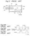
- Fig. 13 schematically shows a vapor growth apparatus for growing GaAs by the MOVPE or ALE method. The apparatus has an approximately cylinder-
shaped reaction tube 101, asupply pipe 102 for supplying trimethyl gallium (TMG) as a Ga material gas into thereaction tube 101, asupply pipe 103 for supplying arsine as an As material gas into thereaction tube 101, and asupply pipe 108 for supplying a purging-use hydrogen gas into thereaction tube 101. Thesupply pipes end surface 101a of thereaction tube 101, and open in an approximately center portion in the axial direction of acylindrical portion 101b of thereaction tube 101. In an approximately center portion in the axial direction of thereaction tube 101 is provided asubstrate holder 105, and thesubstrate holder 105 is supported by anarm member 107 extending from theother end surface 101c of thereaction tube 101. In the case of either the MOVPE method or the ALE method, aGaAs substrate 104 is set on thesubstrate holder 105, and TMG and arsine are supplied respectively through thesupply pipes GaAs substrate 104. Unreacted gas and the like are discharged through anexhaust pipe 110 provided on the side of theother end surface 101c of thecylindrical portion 101b. A major difference between the MOVPE method and the ALE method exists in the timing of supplying the gas. According to the MOVPE method, TMG and arsine are simultaneously supplied. - In contrast to the above, according to the ALE method, the gas supply timing is controlled by opening and closing a control valve (not shown) to alternately supply TMG and arsine. Furthermore, according to the ALE method, there is provided a period in which purging is effected with hydrogen between a TMG supply period and an arsine supply period in a manner as shown in Figs. 14A, 14B, and 14C in order to prevent the TMG and arsine from being mixed with each other. In the period in which purging is effected with hydrogen, a hydrogen gas is supplied into the
reaction tube 101 through thesupply pipe 108, thereby purging the inside of thereaction tube 101. - A feature of the ALE method is to take advantage of a phenomenon that, after a ratio of coating the surface of the
GaAs substrate 104 with TMG or a decomposed substance thereof becomes 1 in the TMG supply period, any further deposition is suppressed (so-called a self-limiting mechanism achieved by appropriately selecting growth conditions such as a substrate temperature). In the arsine supply period subsequent to the TMG supply period, a GaAs monatomic layer is formed on theGaAs substrate 104. By repeating the formation of the monatomic layer, a growth layer having an evenness in units of atomic layers can be obtained. In forming a hetero interface, the interfacial sharpness can be controlled in units of atomic layers. - A required thickness of the semiconductor layer in producing a variety of devices is within a range of several tens angstroms to several micrometers, the range corresponding to a thickness of several tens to several ten thousands atomic layers. Therefore, when it is attempted to grow a semiconductor layer for a variety of devices by the ALE method, the alternate supply of the material gases must be repeated several tens to several ten thousands times per growth layer. However, since the changeover between the gas supply periods has been performed by opening and closing the control valve, the control valve is required to be opened and closed very frequently. Therefore, when a durability of the control valve is taken into account, it has been unrealistic to produce, particularly, mass-produce devices by the ALE method.
- The object of the present invention is therefore to provide a vapor growth apparatus and vapor growth method capable of alternately supplying a cation material gas (e.g., TMG) and an anion material gas (e.g., arsine) onto a substrate without performing such a frequent opening and closing of the control valve, thereby allowing a compound semiconductor layer having an evenness and an interfacial sharpness in units of atomic layers to be grown with a good productivity.
- In order to achieve the aforementioned objective, the present invention provides a vapor growth apparatus for growing a compound semiconductor layer on a surface of a substrate maintained at a specified temperature in a growth chamber by alternately supplying a cation material gas and an anion material gas and reacting the gases, wherein the growth chamber has a cylindrical portion which extends in a direction from an upstream side to a downstream side and an end plate which closes an upstream end portion of the cylindrical portion, the end plate has in specified portions thereof a material gas supply inlet for supplying the cation material gas into the cylindrical portion and a material gas supply inlet for supplying the anion material gas into the cylindrical portion, and further comprising exhaust means for discharging gas inside the cylindrical portion from a downstream side of the cylindrical portion, a substrate holder provided between the upstream side and the downstream side of the cylindrical portion and having a substrate holding surface, gas separation means for forming a plurality of material gas supply areas where the material gases are independently supplied to the substrate holding surface by separating flow paths of the material gases extending from the material gas supply inlets to the substrate holding surface, and drive means for rotating the substrate holder with the substrate set on the substrate holding surface around a center line of the cylindrical portion.
- According to the vapor growth apparatus of the present invention, the growth of the compound semiconductor layer is performed in a manner as follows. A substrate is set on a specified portion of the substrate holding surface of the substrate holder, and the substrate is maintained at a specified temperature appropriate for the growth. In the above-mentioned condition, the cation material gas and the anion material gas are supplied from the material gas supply inlets provided at the end plates of the growth chamber into the cylindrical portion. The supplied material gases are separated from each other by the gas separation means, and reach the substrate holding surface of the substrate holder from the material gas supply inlets without being mixed with each other. Consequently, a plurality of material gas supply areas to which the material gases are independently supplied are formed on the substrate holding surface. In the above place, the substrate holder is made to rotate around the center line of the cylindrical portion. Therefore, the cation material gas and the anion material gas are alternately supplied to the surface of the substrate set on the substrate holding surface. With the above-mentioned operation, a compound semiconductor layer grows on the surface of the substrate in units of atomic layers. Unreacted gas and the like are discharged by the exhaust means on the downstream side. Thus the flow paths of the material gases are separated from each other by the gas separation means, and therefore the cation material gas and the anion material gas can be alternately supplied to the surface of the substrate by rotating the substrate holder. Therefore, the control valve is not required to be frequently opened and closed for the changeover between the gas supply periods unlike the conventional case, resulting in eliminating the fear that the durability of the control valve will be impaired. Therefore, a compound semiconductor layer having an evenness and an interfacial sharpness in units of atomic layers is grown with a good productivity.
- According to the vapor growth apparatus of an embodiment, the substrate holding surface of the substrate holder is perpendicular to the center line of the cylindrical portion and has a circular configuration, and the center of the substrate holding surface exists in the center line of the cylindrical portion.
- With the above-mentioned arrangement, the gap between the substrate holder and the interior wall of the cylindrical portion is made constant with regard to the entire circumference of the substrate holder. Consequently, the conductance of exhaust is made constant with regard to the entire circumference of the substrate holder. Therefore, even when the substrate holder is rotated, no influence is exerted on the flow rate of each material gas. Therefore, the compound semiconductor layer is grown with a good controllability.
- According to the vapor growth apparatus of an embodiment, the gas separation means is comprised of at least one partition plate provided in a plane which includes the center line of the cylindrical portion and passes between the plural number of material gas supply inlets.
- With the above-mentioned arrangement, the flow paths of the material gases are simply effectively separated from each other.
- According to the vapor growth apparatus of an embodiment, the partition plates extend radially from the center line of the cylindrical portion to the interior wall of the cylindrical portion and intersect each other at a specified angle, where the angle is set according to the durations of the periods in which the material gases are supplied to the substrate.
- In the present case, by increasing the setting level of the rotating speed (constant speed) of the substrate holder, the material gas supply periods for forming the compound semiconductor layer are each set at the necessary minimum duration. Therefore, the productivity is increased. Furthermore, since the drive means is required to rotate the substrate holder at a constant speed, a simplified rotation control is achieved.
- According to the vapor growth apparatus of an embodiment, a separation gas supply inlet for supplying separation gas having a characteristic that makes no contribution to growth reaction on the surface of the substrate is provided between the material gas supply inlets at the end plate. The gas separation means is comprised of a flow of the separation gas in a layer form extending from the separation gas supply inlet to the substrate holding surface.
- In the present case, the flow paths of the material gases can be separated from each other without providing any additional member inside the cylindrical portion, thereby allowing a simplified maintenance to be achieved.
- According to the vapor growth apparatus of an embodiment, the substrate holding surface of the substrate holder has a configuration corresponding to an exterior side surface of a pyramidal frustum having a center line coinciding with the center line of the cylindrical portion.
- In the present case, the area of the substrate holding surface can be expanded more than in the case where the substrate holding surface is provided perpendicular to the center line of the cylindrical portion. When the above-mentioned arrangement is adopted, a lot of substrates can be set on the substrate holding surface, thereby allowing an increased productivity to be achieved.
- According to the vapor growth apparatus of an embodiment, the substrate holding surface of the substrate holder has a configuration corresponding to an interior side surface of a prism-shaped pipe having a center line coinciding with the center line of the cylindrical portion.
- With the above-mentioned arrangement, the area of the substrate holding surface can be expanded more than in the case where the substrate holding surface is provided perpendicular to the center line of the cylindrical portion. When the above-mentioned arrangement is adopted, a lot of substrates can be set on the substrate holding surface, whereby an increased productivity is achieved.
- The present invention provides a vapor growth method comprising the steps of: holding a substrate on a substrate holding surface of a substrate holder arranged between an upstream side and a downstream side of a cylindrical portion of a growth chamber having the cylindrical portion which extends in one direction from the upstream side to the downstream side and an end plate which closes an upstream end portion of the cylindrical portion, maintaining the substrate at a specified temperature, forming material gas supply areas where material gases are independently supplied to corresponding portions of the substrate holding surface by supplying a cation material gas and an anion material gas from the upstream side through a plurality of material gas supply inlets into the cylindrical portion while preventing the material gases from being mixed with each other inside the cylindrical portion by gas separation means and discharging the material gases out of the cylindrical portion, and rotating the substrate holder around a center line of the cylindrical portion.
- According to the vapor growth method of an embodiment, the gas separation means is comprised of at least one partition plate arranged in a plane which includes the center line of the cylindrical portion and passes between the plural number of material gas supply inlets, and a rotating speed of the substrate holder is increased when the substrate traverses the plane in which the partition plate exists, and the rotating speed of the substrate holder is reduced or temporarily stopped when the substrate is located in each of the material gas supply areas.
- With the above-mentioned arrangement, the transitional period in which the cation material gas is supplied to a part of the surface of the substrate and the anion material gas is supplied to the remaining part of the surface of the substrate is substantially eliminated. Therefore, growth of an atomic layer having an excellent interfacial sharpness is achieved.
- According to the vapor growth method of an embodiment, the rotating speed of the substrate holder rotating around the center line of the cylindrical portion is changed according to the duration of the period in which each material gas is supplied to the substrate. For instance, when the substrate passes through the supply area of the material gas which requires a short supply time, the rotating speed of the substrate holder is increased. When the substrate passes through the supply area of the material gas which requires a long supply time, the rotating speed of the substrate holder is reduced. With the above-mentioned arrangement, each material gas supply period for forming the compound semiconductor layer is set at the necessary minimum duration. Therefore, an increased productivity is achieved.
- According to the vapor growth method of an embodiment, there are prepared two or more types of at least one of the cation material gas and the anion material gas, and the two or more types of material gases are supplied into the cylindrical portion through different material gas supply inlets, whereby two or more atomic layers are grown in one turn of the substrate holder.
- In the present case, a compound semiconductor layer having a composition of a variety of types is grown.
- The present invention will become more fully understood from the detailed description given hereinbelow and the accompanying drawings which are given by way of illustration only, and thus are not limitative of the present invention, and wherein:
- Fig. 1 is a diagram schematically showing the construction of a vapor growth apparatus according to a first embodiment of the present invention;
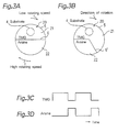
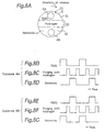
- Fig. 2A is a plan view for explaining a vapor growth method performed by means of the vapor growth apparatus shown in Fig. 1;
- Figs. 2B and 2C are charts for explaining the vapor growth method of Fig. 2A;
- Figs. 3A and 3B are plan views for explaining vapor growth methods which are modifications of the vapor growth method of Fig. 2A.
- Figs. 3C and 3D are charts for explaining the vapor growth methods of Figs. 3A and 3B;
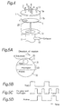
- Fig. 4 is a diagram showing the construction of a vapor growth apparatus according to a second embodiment of the present invention;
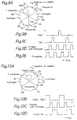
- Fig. 5A is a plan view for explaining a vapor growth method performed by means of the vapor growth apparatus shown in Fig. 4;
- Figs. 5B, 5C and 5D are charts for explaining the vapor growth method of Fig. 5A;
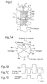
- Fig. 6 is a diagram showing the construction of a vapor growth apparatus according to a third embodiment of the present invention;
- Fig. 7A is a plan view for explaining a vapor growth method performed by means of the vapor growth apparatus shown in Fig. 6;
- Figs. 7B, 7C and 7D are charts for explaining the vapor growth method of Fig. 7A;
- Fig. 8A is a plan view for explaining another vapor growth method performed by means of the vapor growth apparatus shown in Fig. 4;
- Figs. 8B, 8C, 8D, 8E, 8F and 8G are charts for explaining the vapor growth method of Fig. 8A;
- Fig. 9A is a plan view for explaining a vapor growth method performed by means of a modification of the vapor growth apparatus shown in Fig. 6;
- Figs. 9B, 9C, 9D and 9E are charts for explaining the vapor growth method of Fig. 9A;
- Fig. 10A is a plan view for explaining another vapor growth method performed by means of the vapor growth apparatus shown in Fig. 6;
- Figs. 10B, 10C and 10D are charts for explaining the vapor growth method of Fig. 10A;
- Fig. 11 is a diagram showing the construction of a vapor growth apparatus according to a fourth preferred embodiment of the present invention;
- Fig. 12 is a diagram showing the construction of a vapor growth apparatus according to a fifth preferred embodiment of the present invention;
- Fig. 13 is a diagram showing a conventional vapor growth apparatus; and
- Figs. 14A, 14B and 14C are charts for explaining a vapor growth method performed by means of the conventional vapor growth apparatus.
-
- The vapor growth apparatus and vapor growth method of the present invention will be described in detail based on several embodiments thereof with reference to the accompanying drawings.
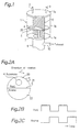
- Fig. 1 shows the construction of a vapor growth apparatus according to a first embodiment of the present invention. The vapor growth apparatus has an approximately cylinder-shaped growth chamber 1. The growth chamber 1 has a
cylindrical portion 1b which extends in a vertical direction, alid portion 1a which serves as an end plate for closing an upstream end portion of thecylindrical portion 1b, and abottom portion 1c for closing the downstream end of thecylindrical portion 1b. At thelid portion 1a, asupply inlet 2 for supplying a cation material gas into the growth chamber 1 and asupply inlet 3 for supplying an anion material gas into the growth chamber 1 are provided in positions symmetrical about the center of thelid portion 1a. Below the growth chamber 1 is vertically provided acylindrical support pipe 9 which has a diameter smaller than that of thecylindrical portion 1b and supports the growth chamber 1. The growth chamber 1 is communicated with thesupport pipe 9 through an opening provided at the center of thebottom portion 1c, and thesupport pipe 9 is communicated with anexhaust pipe 10 provided at a peripheral surface thereof. Gas existing inside thecylindrical portion 1b of the growth chamber 1 is discharged through thesupport pipe 9 and theexhaust pipe 10 by a vacuum pump (not shown) which serves as an exhaust means. Inside thesupport pipe 9 are provided adrive shaft 7 and a drive motor (not shown) which serve as a drive means. - At an approximately middle level of the
cylindrical portion 1b is provided a disk-shapedsubstrate holder 5 horizontally, i.e., perpendicular to the center line of thecylindrical portion 1b. Anupper surface 20 of thesubstrate holder 5 faces the materialgas supply inlets lid portion 1a, and serves as a substrate holding surface on which asubstrate 4 is set in a growth stage. The center of thesubstrate holder 5 exists in the center line of thecylindrical portion 1b, and the outer diameter size of thesubstrate holder 5 is set smaller than the inner diameter size of thecylindrical portion 1b. Consequently, there is achieved a constant gap between thesubstrate holder 5 and the interior wall of thecylindrical portion 1b with regard to the entire circumference. Therefore, a constant conductance of exhaust in a growth stage is achieved with regard to the entire circumference of thesubstrate holder 5. Even when thesubstrate holder 5 is rotated, no influence is exerted on the flow rate of each material gas. Therefore, a compound semiconductor layer can be grown on thesubstrate 4 with a good controllability in a manner as described hereinafter. - The
substrate holder 5 is supported by thedrive shaft 7 extending from the drive motor inside thesupport pipe 9 provided below. The axial center of thedrive shaft 7 coincides with the center line of thecylindrical portion 1b, and a tip end of thedrive shaft 7 is connected to the center of a lower surface of thesubstrate holder 5. In the growth stage, thesubstrate holder 5 is rotated around the center line of thecylindrical portion 1b by the drive motor via thedrive shaft 7. Thesubstrate holder 5 has therein a built-in heater (not shown) which generates heat by receiving an electricity, thereby allowing the entire area of thesubstrate holding surface 20 to be uniformly maintained at a specified temperature in the growth stage. - Inside the
cylindrical portion 1b is provided apartition plate 6 which serves as a gas separation means. Thepartition plate 6 is arranged in a plane which includes the center line of thecylindrical portion 1b and passes between the materialgas supply inlets cylindrical portion 1b into two areas corresponding to the respective materialgas supply inlets partition plate 6 is put in contact with the interior walls of thelid portion 1a, thecylindrical portion 1b, and thebottom portion 1c. In a portion where the above-mentioned plane intersects thesubstrate holder 5 and thedrive shaft 7, thepartition plate 6 is formed with a cut portion along the configurations of themembers members partition plate 6 separates the flow paths of the material gases extending from the materialgas supply inlets substrate holding surface 20 from each other in the growth stage, thereby forming two material gas supply areas where the material gases are independently supplied to thesubstrate holding surface 20. Since thepartition plate 6 is a mere plate, the flow paths of the material gases can be separated from each other simply and effectively. - By means of the above-mentioned vapor growth apparatus, a GaAs layer is to be grown as a compound semiconductor layer on the
GaAs substrate 4. - The
substrate 4 is set between the center and the periphery of thesubstrate holding surface 20 of thesubstrate holder 5. Thesubstrate 4 is maintained at a specified temperature (400 to 550°C) by the built-in heater of thesubstrate holder 5. Under the above-mentioned condition, trimethyl gallium (TMG) which serves as a cation material gas and arsine which serves as an anion material gas are supplied into thecylindrical portion 1b through the materialgas supply inlets cylindrical portion 1b is discharged by the vacuum pump through thesupport pipe 9 and theexhaust pipe 10 provided on the downstream side, whereby a pressure of 20 Torr is achieved inside the growth chamber 1. As a result, a high-speed gas flow is generated inside thecylindrical portion 1b. - The TMG and arsine supplied into the
cylindrical portion 1b through the materialgas supply inlets partition plate 6, and then reach thesubstrate holding surface 20 of thesubstrate holder 5 without being mixed with each other. Consequently, as shown in Fig. 2A, two material gas supply areas (a TMG supply area and an arsine supply area) 21 and 22 to which the TMG and arsine are independently supplied are formed on thesubstrate holding surface 20. In the above-mentioned situation, thesubstrate holder 5 is rotated around the center line of thecylindrical portion 1b by the drive motor. Therefore, the TMG and arsine are alternately supplied to the surface of thesubstrate 4 set on thesubstrate holding surface 20 in a manner as shown in Figs. 2B and 2C. In other words, a gas supply cycle composed of two periods of a TMG supply period and an arsine supply period is formed. Assuming that the rotating speed of thesubstrate holder 5 is six turns per minute (constant speed), theGaAs substrate 4 is put in contact with each of the TMG and arsine for 5 seconds. Through the above-mentioned process, a GaAs monatomic layer (having a thickness of about 2.8 Å) was able to be grown on the surface of thesubstrate 4 every one turn. - As described above, since the flow paths of the material gases are separated from each other by the
partition plate 6 in the present vapor growth apparatus, the cation material gas and the anion material gas can be alternately supplied to the surface of thesubstrate 4 by rotating thesubstrate holder 5. The above-mentioned arrangement obviates the need of frequently opening and closing the control valve for the changeover between the material gas supply periods unlike the conventional case, resulting in eliminating the fear that the durability of the control valve will be impaired. Furthermore, control factors in performing the atomic layer growth by means of the present vapor growth apparatus are growth chamber pressure, substrate temperature, gas flow rate, and the rotating speed of the substrate holder, which can be easily controlled. - Therefore, a compound semiconductor layer having an evenness and an interfacial sharpness in units of atomic layers can be grown with a good productivity. With the above-mentioned arrangement, light emitting devices and high-frequency devices having excellent evenness and interfacial sharpness can be produced.
- Furthermore, since the gas inside the
cylindrical portion 1b is speedily discharged by the vacuum pump, there is generated no convection inside thecylindrical portion 1b. Furthermore, since the gap between thesubstrate holder 5 and the interior wall of thecylindrical portion 1b is made constant with regard to the entire circumference, no influence is exerted on the flow rate of the TMG and arsine even when thesubstrate holder 5 is rotated. Therefore, as described hereinbefore, the GaAs layer can be grown on thesubstrate 4 with a good controllability. - It is to be noted that, when trimethyl aluminum (TMA) is used as the anion material gas instead of TMG, two atomic layers (having a thickness of about 5.7 Å) can be grown in one turn.
- Furthermore, although the rotating speed of the
substrate holder 5 is made constant, the present invention is not limited to this. For instance, it is acceptable to increase the rotating speed of thesubstrate holder 5 when thesubstrate 4 passes just below thepartition plate 6 and reduce the rotating speed or temporarily stop the rotation of thesubstrate holder 5 when thesubstrate 4 is located in a position other than the position just below thepartition plate 6. With the above-mentioned arrangement, a transitional period in which the TMG is supplied to a part of the surface of thesubstrate 4 and the arsine is supplied to the remaining part of the surface of thesubstrate 4 is substantially eliminated. Therefore, growth of an atomic layer having an excellent interfacial sharpness is achieved. - As is known, there is required a time of several seconds to form a TMG monomolecular deposition layer on the
GaAs substrate 4. However, a time shorter than the above-mentioned time is sufficient for the growth of the GaAs monatomic layer through reaction with arsine. In the aforementioned case, it is considered that the arsine supply period is set longer than required. - Therefore, as shown in Fig. 3A, the rotating speed of the
substrate holder 5 may be changed according to the duration of the period in which each of TMG and arsine is supplied to thesubstrate 4. For instance, the rotating speed at the time when thesubstrate 4 passes through thearsine supply area 22 is made greater than the rotating speed at the time when thesubstrate 4 passes through theTMG supply area 21. With the above-mentioned arrangement, the TMG supply period and the arsine supply period for forming the GaAs layer can be each set at the necessary minimum duration in a manner as shown in Fig. 3C. Therefore, the productivity can be increased. - Furthermore, in a manner as shown in Fig. 3B, it is acceptable to make constant the rotating speed of the
substrate holder 5, make a partition plate 6' extend radially from the center line to the interior wall of thecylindrical portion 1b making a specified angle, and set the angle according to the duration of the period in which each of the TMG and arsine is supplied to thesubstrate 4. In the present case, by increasing the setting level of the rotating speed (constant speed) of thesubstrate holder 5, the TMG supply period and the arsine supply period for forming the GaAs layer can be each set at the necessary minimum duration in a manner as shown in Figs. 3C and 3D. Therefore, the productivity can be increased. Furthermore, since thesubstrate holder 5 is allowed to rotate at a constant speed, the rotation control can be easily performed. - Fig. 4 shows the construction of a vapor growth apparatus according to a second embodiment of the present invention. It is to be noted that the same components as those shown in Fig. 1 are denoted by the same reference numerals, and no description therefor is provided herein.
- The present vapor growth apparatus uses a separation gas having a characteristic that makes no contribution to the growth reaction on the surface of the
substrate 4 instead of thepartition plate 6 of the vapor growth apparatus shown in Fig. 1. In detail, separationgas supply inlets gas supply inlets lid portion 1a of the growth chamber 1. In the growth stage, a layer-like flow of the separation gas extending from the separationgas supply inlets substrate holding surface 20 is formed. - By means of the above-mentioned vapor growth apparatus, a GaAs layer is grown as a compound semiconductor layer on the
GaAs substrate 4 in the same manner as in the previous embodiment. Trimethyl gallium (TMG) is used as a cation material gas, arsine is used as an anion material gas, and hydrogen is used as a separation gas. There is provided the same growth condition as that of the previous embodiment, i.e., the condition of a substrate temperature of 400 to 550°C, a pressure of 20 Torr inside the growth chamber 1, a TMG flow rate of 20 SCCM, an arsine flow rate of 200 SCCM, and acceleration of the TMG and arsine with hydrogen gas each at a flow rate of 5 SLM. The flow rate of the separation-use hydrogen gas is set at 10 SLM at each inlet. The rotating speed of thesubstrate holder 5 is six turns per minute (constant speed). - The TMG and arsine supplied into the
cylindrical portion 1b through the materialgas supply inlets substrate holding surface 20 of thesubstrate holder 5 without being mixed with each other. Consequently, as shown in Fig. 5A, aTMG supply area 31 and anarsine supply area 32 are separated from each other by aseparation area 33 achieved by the hydrogen gas on thesubstrate holding surface 20. In the above-mentioned situation, thesubstrate holder 5 is rotated around the center line of thecylindrical portion 1b shown in Fig. 4. Consequently, as shown in Figs. 5B, 5C and 5D, there is formed a gas supply cycle composed of four periods of a TMG supply period, a separation period by means of hydrogen, an arsine supply period, and a separation period by means of hydrogen. With the above-mentioned arrangement, a GaAs monatomic layer was able to be grown on the surface of thesubstrate 4 every one turn. - In the present vapor growth apparatus, the flow paths of the material gases can be separated from each other without providing any additional member inside the
cylindrical portion 1b, which leads to an advantage that the maintenance of the apparatus can be simplified. - It is to be noted that the separation gas is not limited to the hydrogen gas, and the gas is merely required to be a gas having a characteristic that makes no contribution to the growth reaction on the surface of the substrate. For instance, the same effect can be produced when inactive gas such as argon or helium is used.
- Figs. 8A through 8G show an example in which a GaN layer is grown as a compound semiconductor layer on
sapphire substrates - As shown in Fig. 8A, the
substrates substrate holding surface 20 of thesubstrate holder 5 symmetrically about the center, and the substrate temperature is maintained at 500°C. Through the materialgas supply inlets cylindrical portion 1b. The flow rate of TMG is set at 20 SCCM, and acceleration is performed by means of the hydrogen gas of a flow rate of 5 SLM. The flow rate of ammonia is set at 5 SLM. It is to be noted that the separation gas is not flowed in this point of time. The pressure inside the growth chamber 1 is set at 760 Torr by adjusting the displacement of the vacuum pump. The rotating speed of thesubstrate holder 5 is set at about 2000 turns per minute. Since the separation gas is not flowed, the TMG and ammonia are mixed with each other on the twosubstrates substrate holder 5 is increased to the high value of 2000 turns per minute is to ensure a uniformity in thickness of the growth layer. - Subsequently, a GaN atomic layer is grown on the GaN buffer layer. In detail, the substrate temperature is elevated and maintained within a range of 800 to 1000°C. With the flow rates of the TMG and ammonia kept intact, hydrogen gas is flowed through the separation
gas supply inlets substrate holder 5 is set at about 10 turns per minute. - The TMG and ammonia supplied into the
cylindrical portion 1b through the materialgas supply inlets substrate holding surface 20 of thesubstrate holder 5 without being mixed with each other. Consequently, in a manner as shown in Fig. 8A, aTMG supply area 51 and anammonia supply area 52 are separated from each other by aseparation area 53 achieved by the hydrogen gas on thesubstrate holding surface 20. In the above-mentioned situation, thesubstrate holder 5 is rotated around the center line of thecylindrical portion 1b shown in Fig. 4. Consequently, in regard to thesubstrate 4A, as shown in Figs. 8B to 8D, there is formed a gas supply cycle composed of four periods of a TMG supply period, a separation period by means of hydrogen, an ammonia supply period, and a separation period by means of hydrogen. On the other hand, in regard to thesubstrate 4B, as shown in Figs. 8E to 8G, there is formed a gas supply cycle composed of four periods of an ammonia supply period, a separation period by means of hydrogen, a TMG supply period, and a separation period by means of hydrogen in a phase reverse to that of thesubstrate 4A. Although the gas supply cycles of thesubstrates substrates - It is to be noted that the number of substrates is of course not limited to two, and there may be any number of substrates so long as the substrates can be mounted on the
substrate holding surface 20. - Fig. 6 shows the construction of a vapor growth apparatus according to a third embodiment of the present invention. It is to be noted that the same components as those shown in Figs. 1 and 4 are denoted by the same reference numerals, and no description therefor is provided herein.
- The present vapor growth apparatus concurrently uses
partition plates gas supply inlets gas supply inlets lid portion 1a of the growth chamber 1. On the other hand, inside thecylindrical portion 1b are providedpartition plates partition plates cylindrical portion 1b, thereby separating the inside of thecylindrical portion 1b into four areas corresponding to the materialgas supply inlets gas supply inlets partition plates substrate 4. Thepartition plates gas supply inlets gas supply inlets substrate holding surface 20 in the growth stage. Since thepartition plates - A zinc selenide layer is to be grown as a compound semiconductor layer on a
GaAs substrate 4. Diethyl zinc (DEZ) of one system is used as a cation material gas, hydrogen selenide of one system is used as an anion material gas, and hydrogen of two systems are used as a separation gas. There is provided a growth condition of a substrate temperature of 200 to 300°C, a pressure of 10 Torr inside the growth chamber 1, a DEZ flow rate of 10 SCCM, a hydrogen selenide flow rate of 200 SCCM, and acceleration of each of the DEZ and hydrogen selenide with hydrogen gas each at a flow rate of 3 SLM. The flow rate of the separation-use hydrogen gas is 5 SLM at each inlet. The rotating speed of thesubstrate holder 5 is ten turns per minute (constant speed). - As shown in Figs. 6 and 7A, the DEZ, hydrogen selenide, and hydrogen of two systems supplied into the
cylindrical portion 1b through the materialgas supply inlets gas supply inlets partition plates substrate holding surface 20 of thesubstrate holder 5 without being mixed with each other. In the present example, as shown in Fig. 7A, aDEZ supply area 41, aseparation area 42 by means of hydrogen, a hydrogenselenide supply area 43, and aseparation area 44 by means of hydrogen are sequentially formed on thesubstrate holding surface 20 in the circumferential direction. In the above-mentioned situation, thesubstrate holder 5 is rotated around the center line of thecylindrical portion 1b shown in Fig. 6. Consequently, as shown in Figs. 7B, 7C and 7D, there is formed a gas supply cycle composed of four periods of a DEZ supply period, a separation period by means of hydrogen, a hydrogen selenide supply period, and a separation period by means of hydrogen. With the above-mentioned arrangement, a zinc selenide monatomic layer (having a thickness of about 2.8 Å) was able to be grown on the surface of thesubstrate 4 every one turn. - It is to be noted that the number of partition plates is not limited to two. Three or more partition plates may be provided and made to intersect each other in the center line of the
cylindrical portion 1b at specified angles. When the above-mentioned arrangement is adopted, the supply systems of material gases and separation gas can be increased in number by providing a supply system of a material gas or a supply system of a separation gas for every area separated by the partition plates. Therefore, various types of compound semiconductor layers can be grown on the substrate. - Figs. 9A, 9B, 9C, 9D, and 9E show an example in which a Ga0.5In0.5P layer is grown as a compound semiconductor layer on a
GaAs substrate 4 by means of a vapor growth apparatus of which partition plates are increased in number to three and the other parts of which are similar to those of Fig. 3. - The vapor growth apparatus used herein concurrently uses
partition plates partition plates cylindrical portion 1b shown in Fig. 6. The angles at which thepartition plates substrate 4. There are used material gases of three types of four systems. In detail, one system of TMG and one system of trimethyl indium (TMI) are used as a cation material gas. There is used phosphine of two systems as an anion material gas. There is provided a growth condition of a substrate temperature of 300 to 500°C, a pressure of 20 Torr inside the growth chamber 1, a TMG flow rate of 10 SCCM, a TMI flow rate of 10 SCCM, a phosphine flow rate of 100 SCCM at each area, and acceleration of the TMG, TMI, and phosphine with hydrogen gas each at a flow rate of 3 SLM. The flow rate of the separation-use hydrogen gas is 3 SLM. The rotating speed of thesubstrate holder 5 is three turns per minute (constant speed). - The TMG, TMI, phosphine of two systems, and hydrogen of two systems supplied into the
cylindrical portion 1b through the material gas supply inlets are separated from each other by thepartition plates substrate holding surface 20 of thesubstrate holder 5 without being mixed with each other. In the present example, in a manner as shown in Fig. 9A, aTMG supply area 61, aphosphine supply area 62, aseparation area 63 by means of hydrogen, aTMI supply area 64, aphosphine supply area 65, and aseparation area 66 by means of hydrogen are sequentially formed in the circumferential direction on thesubstrate holding surface 20. In the above-mentioned situation, thesubstrate holder 5 is rotated around the center line of thecylindrical portion 1b shown in Fig. 6. Consequently, there is formed a gas supply cycle composed of six periods of a TMG supply period, a phosphine supply period, a separation period by means of hydrogen, a TMI supply period, a phosphine supply period, and a separation period by means of hydrogen in a manner as shown in Figs. 9B, 9C, 9D and 9E. - With the above-mentioned arrangement, a pair of superlattice structures of (GaP)1(InP)1 (having a thickness of about 5.6 Å) was able to be grown on the surface of the
substrate 4 every one turn. A stack of the above-mentioned superlattice structures functions as a Ga0.5In0.5P layer. - Figs. 10A, 10B, 10C and 10D show an example in which a Ga0.5In0.5P layer is grown as a compound semiconductor layer on a
GaAs substrate 4 by means of the vapor growth apparatus shown in Fig. 6. - In a manner as shown in Fig. 10A, there are used TMG and TMI (referred to as (TMG + TMI)) as a cation material gas to be supplied concurrently to one system, and phosphine of one system is used as an anion material gas. There is used hydrogen of two systems as a separation gas. There is provided a growth condition of a substrate temperature of 300 to 500°C, a pressure of 20 Torr inside the growth chamber 1, a TMG flow rate of 5 SCCM, a TMI flow rate of 10 SCCM, a phosphine flow rate of 200 SCCM, and acceleration of the TMG, TMI, and phosphine with hydrogen gas each at a flow rate of 3 SLM. The flow rate of the separation-use hydrogen gas is 3 SLM. The rotating speed of the
substrate holder 5 is three turns per minute (constant speed). - In the present example, a (TMG + TMI)
supply area 71, aseparation area 72 by means of hydrogen, aphosphine supply area 73, and aseparation area 74 by means of hydrogen are sequentially formed in the circumferential direction on thesubstrate holding surface 20. In the above-mentioned situation, thesubstrate holder 5 is rotated around the center line of thecylindrical portion 1b shown in Fig. 6. Consequently, as shown in Figs. 10B, 10C and 10D, there is formed a gas supply cycle composed of four periods of a (TMG + TMI) supply period, a separation period by means of hydrogen, a phosphine supply period, and a separation period by means of hydrogen. - With the above-mentioned arrangement, a Ga0.5In0.5 p monatomic layer (having a thickness of about 2.8 Å) was able to be grown on the surface of the
substrate 4 every one turn. - Although the compound semiconductor layer grown on the substrate has a composition of one type in each of the aforementioned examples, the compound semiconductor layer may have compositions of a variety of types by changing the type of the material gas in the course of the growth process. Furthermore, in order to give a conductivity to the compound semiconductor layer to be grown, a material gas containing an impurity element may be used.
- Although an organic metal compound is used as a cation material gas in each of the aforementioned examples, there may be used a material gas other than the organic metal compound, such as a halogen compound.
- Although the growth chamber 1 has the
cylindrical portion 1b which extends in a vertical direction in each of the vapor growth apparatuses shown in Figs. 1, 4, and 6, the present invention is not limited to this. It is acceptable to arrange the cylindrical portion in a horizontal direction and flow the material gases and separation gas in the horizontal direction. - The
substrate holder 5 may be a high-frequency heating type effected with provision of a coil around thecylindrical portion 1b instead of the built-in heater type. - Fig. 11 shows the construction of a vapor growth apparatus according to a fourth preferred embodiment of the present invention. It is to be noted that the same components as those shown in Fig. 1 are denoted by the same reference numerals, and no description therefor is provided herein.
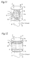
- In the present vapor growth apparatus, an approximately cone frustum-shaped
substrate holder 15 having a center line coinciding with the center line of thecylindrical portion 1b is provided at an approximately middle level of thecylindrical portion 1b. Anexterior side surface 30 of thesubstrate holder 15 has a pyramidal configuration (pyramidal configuration having a polygonal transverse section) rather than a conical configuration. Each segmented small surface between adjacent ridgelines of theexterior side surface 30 has a flatness such that it can allow asubstrate 4 to adhere thereto, and serves as a substrate holding surface on which thesubstrate 4 is set in the growth stage. In the case of thepresent substrate holder 15, the area of thesubstrate holding surface 30 can be expanded more than in the case where the substrate holding surface is provided horizontally. Therefore, a lot ofsubstrates substrate holding surface 30, which resulting in an improved productivity. - In the present example, a lower edge of the
substrate holder 15 has a circular configuration, and its outer diameter size is set smaller than the inner diameter size of thecylindrical portion 1b. The center line of thesubstrate holder 15 is coinciding with the center line of thecylindrical portion 1b, and consequently a gap between the lower edge and the interior wall of thecylindrical portion 1b is made constant throughout the entire circumference. Therefore, the conductance of exhaust is made constant with regard to the entire circumference of thesubstrate holder 15. Even when thesubstrate holder 15 is rotated, no influence is exerted on the flow velocity of each material gas. Therefore, a compound semiconductor layer can be grown on thesubstrate 4 with a good controllability. - Furthermore, a
partition plate 16 having a cut portion along the configurations of thesubstrate holder 15 and thedrive shaft 7 is provided as a gas separation means inside thecylindrical portion 1b. Thepartition plate 16 is provided in a plane which includes the center line of thecylindrical portion 1b and passes between the materialgas supply inlets cylindrical portion 1b into two areas corresponding respectively to the materialgas supply inlets partition plate 16, a cation material gas and an anion material gas can be alternately supplied to the surface of thesubstrate 4 by rotating thesubstrate holder 15. Therefore, a compound semiconductor layer having an evenness and an interfacial sharpness in units of atomic layers can be grown with a good productivity. With the above-mentioned arrangement, light emitting devices and high-frequency devices having excellent evenness and interfacial sharpness can be produced. - Fig. 12 shows the construction of a vapor growth apparatus according to a fifth preferred embodiment of the present invention. It is to be noted that the same components as those shown in Fig. 1 are denoted by the same reference numerals, and no description therefor is provided herein.
- In the present vapor growth apparatus, an approximately cylinder-shaped
substrate holder 25 having a center line coinciding with the center line of thecylindrical portion 1b is provided inside thecylindrical portion 1b. Thesubstrate holder 25 is supported by thedrive shaft 7 which extends from the drive motor inside thesupport pipe 9 provided below and arm members (not shown) which extends from the circumference of thedrive shaft 7 to a lower end of thesubstrate holder 25. Aninterior surface 40 of thesubstrate holder 25 has a prismatic configuration (prismatic configuration having a polygonal transverse section) rather than a cylindrical configuration. Each segmented small surface between adjacent valleys lines of theinterior surface 40 has a flatness such that it can allow asubstrate 4 to adhere thereto, and serves as a substrate holding surface on which thesubstrate 4 is set in the growth stage. In the case of thesubstrate holder 25, the area of thesubstrate holding surface 40 can be expanded more than in the case where the substrate holding surface is provided horizontally, Therefore, a lot ofsubstrates substrate holding surface 40, which resulting in an improved productivity. - In the present case, the
substrate holder 25 has an approximately cylinder-shaped configuration. Therefore, even when thesubstrate holder 25 rotates in the growth stage, no influence is exerted on the speed of flow of each material gas. Therefore, a compound semiconductor layer can be grown on thesubstrate 4 with a good controllability. - Furthermore, a
partition plate 26 having an approximately T-shaped configuration is provided as a gas separation means inside thecylindrical portion 1b. Thepartition plate 26 is provided in a plane which includes the center line of thecylindrical portion 1b and passes between the materialgas supply inlets cylindrical portion 1b into two areas corresponding respectively to the materialgas supply inlets partition plate 26, a cation material gas and an anion material gas can be alternately supplied to the surface of thesubstrate 4 by rotating thesubstrate holder 25. Therefore, a compound semiconductor layer having an evenness and an interfacial sharpness in units of atomic layers can be grown with a good productivity. With the above-mentioned arrangement, light emitting devices and high-frequency devices having excellent evenness and interfacial sharpness can be produced. - As is apparent from the above description, the flow paths of the material gases are separated from each other by the gas separation means in the vapor growth apparatus of the present invention, and therefore the cation material gas and the anion material gas can be alternately supplied to the surface of the substrate by rotating the substrate holder. With the above-mentioned arrangement, the control valve is not required to be frequently opened and closed for the changeover between the material gas supply periods unlike the conventional case, resulting in eliminating the fear that the durability of the control valve will be impaired. Further, a compound semiconductor layer having an evenness and an interfacial sharpness in units of atomic layers can be grown with a good productivity.
- According to the vapor growth apparatus of an embodiment, the substrate holding surface of the substrate holder is perpendicular to the center line of the cylindrical portion and has a circular configuration, and the center of the substrate holding surface exists in the center line of the cylindrical portion. With the above-mentioned arrangement, the gap between the substrate holder and the interior wall of the cylindrical portion is made constant with regard to the entire circumference of the substrate holder. Consequently, the conductance of exhaust is made constant with regard to the entire circumference of the substrate holder. Therefore, even when the substrate holder is rotated, no influence is exerted on the flow speed of each material gas, and a compound semiconductor layer can be grown with a good controllability.
- According to the vapor growth apparatus of an embodiment, the gas separation means is comprised of at least one partition plate provided in a plane which includes the center line of the cylindrical portion and passes between the plural number of material gas supply inlets. With the above-mentioned arrangement, the flow paths of the material gases can be simply effectively separated from each other.
- According to the vapor growth apparatus of an embodiment, the partition plates extend radially from the center line to the interior wall of the cylindrical portion and intersect each other at a specified angle, and the angle is set according to a duration of a period in which each of the material gases are supplied to the substrate. Therefore, by increasing the setting level of the rotating speed (constant speed) of the substrate holder, each material gas supply period for forming the compound semiconductor layer can be set at the necessary minimum duration. Therefore, the productivity can be increased. Furthermore, since the drive means is merely required to rotate the substrate holder at a constant speed, the rotation control can be performed simply.
- According to the vapor growth apparatus of an embodiment, a separation gas supply inlet for supplying the separation gas having a characteristic that makes no contribution to the growth reaction on the surface of the substrate is provided between the plural number of material gas supply inlets at the end plate. The gas separation means is comprised of a flow of the separation gas in a layer form extending from the separation gas supply inlet to the substrate holding surface. Therefore, the flow paths of the material gases can be separated from each other without providing any additional member inside the cylindrical portion, thereby allowing a simplified maintenance to be achieved.
- According to the vapor growth apparatus of an embodiment, the substrate holding surface of the substrate holder has a configuration corresponding to the exterior side surface of a pyramidal frustum having a center line coinciding with the center line of the cylindrical portion. With the above-mentioned arrangement, the area of the substrate holding surface can be expanded more than in the case where the substrate holding surface is provided perpendicular to the center line of the cylindrical portion. Therefore, a lot of substrates can be set on the substrate holding surface, whereby an increased productivity is achieved.
- According to the vapor growth apparatus of an embodiment, the substrate holding surface of the substrate holder has a configuration corresponding to the interior side surface of a prism-shaped pipe having a center line coinciding with the center line of the cylindrical portion. With the above-mentioned arrangement, the area of the substrate holding surface can be expanded more than in the case where the substrate holding surface is provided perpendicular to the center line of the cylindrical portion. Therefore, a lot of substrates can be set on the substrate holding surface, whereby an increased productivity is achieved.
- The present invention also provides a vapor growth method comprising the steps of: holding a substrate on a substrate holding surface of a substrate holder arranged between an upstream side and a downstream side of a cylindrical portion of a growth chamber having the cylindrical portion which extends in one direction from the upstream side to the downstream side and an end plate which closes an upstream end portion of the cylindrical portion, maintaining the substrate at a specified temperature; farming material gas supply areas where material gases are independently supplied to corresponding portions of the substrate holding surface by supplying a cation material gas and an anion material gas from the upstream side through a plurality of material gas supply inlets into the cylindrical portion while preventing the material gases from being mixed with each other inside the cylindrical portion by gas separation means and discharging the material gases out of the cylindrical portion, and rotating the substrate holder around a center line of the cylindrical portion.
- According to the vapor growth method of the present invention, the cation material gas and the anion material gas can be alternately supplied to the surface of the substrate by rotating the substrate holder while preventing the material gases from being mixed by the separation means, and a compound semiconductor layer having an evenness and an interfacial sharpness in units of atomic layers can be grown with a good productivity. Furthermore, the above-mentioned arrangement obviates the need of frequently opening and closing the control valve.
- According to the vapor growth method of an embodiment, the rotating speed of the substrate holder is increased when the substrate traverses the plane in which the partition plate exists, and the rotating speed of the substrate holder is reduced or temporarily stopped when the substrate is located in each material gas supply area. With the above-mentioned arrangement, a transitional period in which the cation material gas is supplied to a part of the surface of the substrate and the anion material gas is supplied to the remaining part of the surface of the substrate can be substantially eliminated. Therefore, growth of an atomic layer having an excellent interfacial sharpness can be achieved.
- According to the vapor growth method of an embodiment, the rotating speed of the substrate holder rotating around the center line of the cylindrical portion is changed according to the duration of the period in which each material gas is supplied to the substrate. For instance, when the substrate passes through the supply area of the material gas which requires a short supply time, the rotating speed of the substrate holder is increased. When the substrate passes through the supply area of the material gas which requires a long supply time, the rotating speed of the substrate holder is reduced. With the above-mentioned arrangement, each material gas supply period for forming the compound semiconductor layer can be set at the necessary minimum duration. Therefore, the productivity can be increased.
- According to the vapor growth method of an embodiment, there are prepared two or more types of at least one of the cation material gas and the anion material gas, and the two or more types of material gases are supplied into the cylindrical portion through different material gas supply inlets, whereby two or more atomic layers are grown in one turn of the substrate holder. Therefore, a compound semiconductor layer having a composition of a variety of types can be grown.
- The invention being thus described, it will be obvious that the same may be varied in many ways. Such variations are not to be regarded as a departure from the spirit and scope of the invention, and all such modifications as would be obvious to one skilled in the art are intended to be included within the scope of the following claims.
- SCCM and SLM represent units of flow rate. "S" is an abbreviation for the standard condition in which the temperature is 0 C and the pressure is 1 atm, and means that the volume of gas under a certain condition is converted into the volume of the gas under the standard condition. "CC" is an abbreviation for cubic centimeter. "L" is an abbreviation for liter, and "M" means "per minute". Therefore, for example "1SCCM" means that the gas of 1 cc if converted to the standard condition flows per minute. "1SLM" means that the gas of 1 liter if converted to the standard condition flow per minute.
Claims (5)
- A vapour growth apparatus for growing a compound semiconductor layer on a surface of a substrate (4) maintained at a specified temperature in a growth chamber (1) by alternatively supplying a cation material gas and an anion material gas to the substrate and reacting the gases, whereinthe growth chamber (1) has a cylindrical portion (1b) which extends in a direction from an upstream side to a downstream side and an end plate (1a) which closes an upstream end portion of the cylindrical portion (1b),the end plate (1a) has a first material gas supply inlet (2) for supplying the cation material gas into the cylindrical portion (1b) and a second material gas supply inlet (3) for supplying the anion material gas into the cylindrical portion (1b), the apparatus further comprisingexhaust means (10) for discharging gas inside the cylindrical portion (1b) from a downstream side of the cylindrical portion (1b),a substrate holder (25) provided between the upstream side and the downstream side of the cylindrical portion (1b) and having a substrate holding surface (40),gas separation means (6, 16, 26) for forming a plurality of material gas supply areas where the material gases are independently supplied to the substrate holding surface (40) by separating flow paths of the material gases extending from the material gas supply inlets (2, 3) to the substrate holding surface (40), anddrive means for rotating the substrate holder (25) with the substrate (4) set on the substrate holding surface (40) around a centre line of the cylindrical portion (1b);the vapour growth apparatus being characterised in that the substrate holding surface (40) of the substrate holder (25) has a configuration corresponding to the interior surface of a cylindrical prism having a centre line coinciding with the centre line of the cylindrical portion (1b).
- A vapour growth apparatus as claimed in Claim 1, whereinthe gas separation means comprises at least one partition plate (6, 6', 6A, 6B, 16, 26) provided in a plane which includes the centre line of the cylindrical portion (1b) and passes between the material gas supply inlets (2, 3).
- A vapour growth method comprising the steps ofholding a substrate (4) on a substrate holding surface (20, 30, 40) of a substrate holder (5, 15, 25) arranged between an upstream side and a downstream side of a cylindrical portion (1b) of a growth chamber (1), the growth chamber having the cylindrical portion (1b) and an end plate (1a) which closes an upstream end portion of the cylindrical portion (1b), the cylindrical portion (1b) of the growth chamber extending in one direction from the upstream side of the growth chamber to the downstream side,maintaining the substrate (4) at a specified temperature,forming material gas supply areas (71,73) where material gases are independently supplied to respective portions of the substrate holding surface (20, 30, 40) by supplying a cation material gas and an anion material gas into the upstream side of the cylindrical portion (1b) of the growth chamber through a plurality of material gas supply inlets (2, 3) while preventing the material gases from mixing with each other inside the cylindrical portion (1b) by gas separation means (6, 16, 26), and subsequently discharging the material gases out of the cylindrical portion (1b), androtating the substrate holder (5, 15, 25) around a centre line of the cylindrical portion (1b);the method being characterised in that two or more different cation material gases, or two or more different anion material gases, are supplied to the growth chamber (1) during one revolution of the substrate holder.
- A method as claimed in claim 3 wherein the two or more different cation material gases, or the two or more different anion material gases, are supplied into the cylindrical portion (1b) of the growth chamber (1) through separate material gas supply inlets (2, 3), whereby layers of two or more different compounds are grown in one revolution of the substrate holder.
- A method as claimed in claim 3 wherein the two or more different cation material gases, or the two or more different anion material gases, are supplied to one material gas supply area (71) of the growth chamber (1).
Applications Claiming Priority (3)
| Application Number | Priority Date | Filing Date | Title |
|---|---|---|---|
| JP10676094A JP3181171B2 (en) | 1994-05-20 | 1994-05-20 | Vapor phase growth apparatus and vapor phase growth method |
| JP10676094 | 1994-05-20 | ||
| EP95303333A EP0683249B1 (en) | 1994-05-20 | 1995-05-18 | Method for the growth of compound semiconductor layer |
Related Parent Applications (1)
| Application Number | Title | Priority Date | Filing Date |
|---|---|---|---|
| EP95303333A Division EP0683249B1 (en) | 1994-05-20 | 1995-05-18 | Method for the growth of compound semiconductor layer |
Publications (3)
| Publication Number | Publication Date |
|---|---|
| EP0964083A2 true EP0964083A2 (en) | 1999-12-15 |
| EP0964083A3 EP0964083A3 (en) | 2002-01-30 |
| EP0964083B1 EP0964083B1 (en) | 2004-07-14 |
Family
ID=14441872
Family Applications (2)
| Application Number | Title | Priority Date | Filing Date |
|---|---|---|---|
| EP99202642A Expired - Lifetime EP0964083B1 (en) | 1994-05-20 | 1995-05-18 | Apparatus for growing a compound semiconductor layer |
| EP95303333A Expired - Lifetime EP0683249B1 (en) | 1994-05-20 | 1995-05-18 | Method for the growth of compound semiconductor layer |
Family Applications After (1)
| Application Number | Title | Priority Date | Filing Date |
|---|---|---|---|
| EP95303333A Expired - Lifetime EP0683249B1 (en) | 1994-05-20 | 1995-05-18 | Method for the growth of compound semiconductor layer |
Country Status (7)
| Country | Link |
|---|---|
| US (1) | US5730802A (en) |
| EP (2) | EP0964083B1 (en) |
| JP (1) | JP3181171B2 (en) |
| KR (1) | KR0173013B1 (en) |
| CN (1) | CN1060233C (en) |
| DE (2) | DE69515926T2 (en) |
| TW (1) | TW265458B (en) |
Cited By (1)
| Publication number | Priority date | Publication date | Assignee | Title |
|---|---|---|---|---|
| NL1014734C2 (en) * | 2000-03-23 | 2001-09-25 | Huga Optotech Inc | Production of an epitaxial layer on a single crystalline substrate comprises heating a purified substrate in an epitaxy device while introducing organometallic precursors and a nitrogen-containing gas at a specified flow rate |
Families Citing this family (376)
| Publication number | Priority date | Publication date | Assignee | Title |
|---|---|---|---|---|
| WO1997036320A1 (en) * | 1996-03-22 | 1997-10-02 | Nippon Sanso Corporation | Vapor phase growth apparatus and vapor phase growth method |
| US6342277B1 (en) * | 1996-08-16 | 2002-01-29 | Licensee For Microelectronics: Asm America, Inc. | Sequential chemical vapor deposition |
| US5807792A (en) * | 1996-12-18 | 1998-09-15 | Siemens Aktiengesellschaft | Uniform distribution of reactants in a device layer |
| US6671223B2 (en) * | 1996-12-20 | 2003-12-30 | Westerngeco, L.L.C. | Control devices for controlling the position of a marine seismic streamer |
| US5888886A (en) * | 1997-06-30 | 1999-03-30 | Sdl, Inc. | Method of doping gan layers p-type for device fabrication |
| DE60008241T2 (en) * | 1999-05-13 | 2004-07-01 | Emf Ireland Ltd., Riverstown | METHOD AND DEVICE FOR EPITACTICALLY GROWING A MATERIAL ON A SUBSTRATE |
| US6620723B1 (en) * | 2000-06-27 | 2003-09-16 | Applied Materials, Inc. | Formation of boride barrier layers using chemisorption techniques |
| US6551929B1 (en) | 2000-06-28 | 2003-04-22 | Applied Materials, Inc. | Bifurcated deposition process for depositing refractory metal layers employing atomic layer deposition and chemical vapor deposition techniques |
| US7964505B2 (en) * | 2005-01-19 | 2011-06-21 | Applied Materials, Inc. | Atomic layer deposition of tungsten materials |
| US7101795B1 (en) | 2000-06-28 | 2006-09-05 | Applied Materials, Inc. | Method and apparatus for depositing refractory metal layers employing sequential deposition techniques to form a nucleation layer |
| US7405158B2 (en) | 2000-06-28 | 2008-07-29 | Applied Materials, Inc. | Methods for depositing tungsten layers employing atomic layer deposition techniques |
| US7732327B2 (en) | 2000-06-28 | 2010-06-08 | Applied Materials, Inc. | Vapor deposition of tungsten materials |
| KR100458982B1 (en) * | 2000-08-09 | 2004-12-03 | 주성엔지니어링(주) | Semiconductor device fabrication apparatus having rotatable gas injector and thin film deposition method using the same |
| JP4511006B2 (en) * | 2000-09-01 | 2010-07-28 | 独立行政法人理化学研究所 | Impurity doping method of semiconductor |
| US6765178B2 (en) * | 2000-12-29 | 2004-07-20 | Applied Materials, Inc. | Chamber for uniform substrate heating |
| US6825447B2 (en) * | 2000-12-29 | 2004-11-30 | Applied Materials, Inc. | Apparatus and method for uniform substrate heating and contaminate collection |
| US6998579B2 (en) | 2000-12-29 | 2006-02-14 | Applied Materials, Inc. | Chamber for uniform substrate heating |
| US20020083897A1 (en) * | 2000-12-29 | 2002-07-04 | Applied Materials, Inc. | Full glass substrate deposition in plasma enhanced chemical vapor deposition |
| US20020127336A1 (en) * | 2001-01-16 | 2002-09-12 | Applied Materials, Inc. | Method for growing thin films by catalytic enhancement |
| US6811814B2 (en) | 2001-01-16 | 2004-11-02 | Applied Materials, Inc. | Method for growing thin films by catalytic enhancement |
| US6951804B2 (en) | 2001-02-02 | 2005-10-04 | Applied Materials, Inc. | Formation of a tantalum-nitride layer |
| US6878206B2 (en) * | 2001-07-16 | 2005-04-12 | Applied Materials, Inc. | Lid assembly for a processing system to facilitate sequential deposition techniques |
| US6660126B2 (en) | 2001-03-02 | 2003-12-09 | Applied Materials, Inc. | Lid assembly for a processing system to facilitate sequential deposition techniques |
| US6734020B2 (en) | 2001-03-07 | 2004-05-11 | Applied Materials, Inc. | Valve control system for atomic layer deposition chamber |
| US6849545B2 (en) | 2001-06-20 | 2005-02-01 | Applied Materials, Inc. | System and method to form a composite film stack utilizing sequential deposition techniques |
| US7211144B2 (en) * | 2001-07-13 | 2007-05-01 | Applied Materials, Inc. | Pulsed nucleation deposition of tungsten layers |
| US20070009658A1 (en) * | 2001-07-13 | 2007-01-11 | Yoo Jong H | Pulse nucleation enhanced nucleation technique for improved step coverage and better gap fill for WCVD process |
| US20080268635A1 (en) * | 2001-07-25 | 2008-10-30 | Sang-Ho Yu | Process for forming cobalt and cobalt silicide materials in copper contact applications |
| US20030029715A1 (en) * | 2001-07-25 | 2003-02-13 | Applied Materials, Inc. | An Apparatus For Annealing Substrates In Physical Vapor Deposition Systems |
| JP2005504885A (en) * | 2001-07-25 | 2005-02-17 | アプライド マテリアルズ インコーポレイテッド | Barrier formation using a novel sputter deposition method |
| US8110489B2 (en) * | 2001-07-25 | 2012-02-07 | Applied Materials, Inc. | Process for forming cobalt-containing materials |
| US9051641B2 (en) * | 2001-07-25 | 2015-06-09 | Applied Materials, Inc. | Cobalt deposition on barrier surfaces |
| US20090004850A1 (en) | 2001-07-25 | 2009-01-01 | Seshadri Ganguli | Process for forming cobalt and cobalt silicide materials in tungsten contact applications |
| US7085616B2 (en) | 2001-07-27 | 2006-08-01 | Applied Materials, Inc. | Atomic layer deposition apparatus |
| DE10141084A1 (en) * | 2001-08-22 | 2002-11-28 | Infineon Technologies Ag | Apparatus for depositing layers having atomic thickness on a substrate used in the semiconductor industry has a chamber wall arranged between two chamber regions to separate the chamber regions |
| US6718126B2 (en) * | 2001-09-14 | 2004-04-06 | Applied Materials, Inc. | Apparatus and method for vaporizing solid precursor for CVD or atomic layer deposition |
| US20030059538A1 (en) * | 2001-09-26 | 2003-03-27 | Applied Materials, Inc. | Integration of barrier layer and seed layer |
| US7049226B2 (en) * | 2001-09-26 | 2006-05-23 | Applied Materials, Inc. | Integration of ALD tantalum nitride for copper metallization |
| US6936906B2 (en) * | 2001-09-26 | 2005-08-30 | Applied Materials, Inc. | Integration of barrier layer and seed layer |
| US6916398B2 (en) * | 2001-10-26 | 2005-07-12 | Applied Materials, Inc. | Gas delivery apparatus and method for atomic layer deposition |
| US7780785B2 (en) | 2001-10-26 | 2010-08-24 | Applied Materials, Inc. | Gas delivery apparatus for atomic layer deposition |
| KR100782529B1 (en) * | 2001-11-08 | 2007-12-06 | 에이에스엠지니텍코리아 주식회사 | Apparatus for depositing |
| US6729824B2 (en) | 2001-12-14 | 2004-05-04 | Applied Materials, Inc. | Dual robot processing system |
| US6911092B2 (en) * | 2002-01-17 | 2005-06-28 | Sundew Technologies, Llc | ALD apparatus and method |
| AU2003238853A1 (en) * | 2002-01-25 | 2003-09-02 | Applied Materials, Inc. | Apparatus for cyclical deposition of thin films |
| US6866746B2 (en) * | 2002-01-26 | 2005-03-15 | Applied Materials, Inc. | Clamshell and small volume chamber with fixed substrate support |
| US6998014B2 (en) | 2002-01-26 | 2006-02-14 | Applied Materials, Inc. | Apparatus and method for plasma assisted deposition |
| US6911391B2 (en) | 2002-01-26 | 2005-06-28 | Applied Materials, Inc. | Integration of titanium and titanium nitride layers |
| US6827978B2 (en) * | 2002-02-11 | 2004-12-07 | Applied Materials, Inc. | Deposition of tungsten films |
| US6833161B2 (en) * | 2002-02-26 | 2004-12-21 | Applied Materials, Inc. | Cyclical deposition of tungsten nitride for metal oxide gate electrode |
| US6972267B2 (en) | 2002-03-04 | 2005-12-06 | Applied Materials, Inc. | Sequential deposition of tantalum nitride using a tantalum-containing precursor and a nitrogen-containing precursor |
| US6800134B2 (en) | 2002-03-26 | 2004-10-05 | Micron Technology, Inc. | Chemical vapor deposition methods and atomic layer deposition methods |
| US7439191B2 (en) * | 2002-04-05 | 2008-10-21 | Applied Materials, Inc. | Deposition of silicon layers for active matrix liquid crystal display (AMLCD) applications |
| US6846516B2 (en) * | 2002-04-08 | 2005-01-25 | Applied Materials, Inc. | Multiple precursor cyclical deposition system |
| US6720027B2 (en) | 2002-04-08 | 2004-04-13 | Applied Materials, Inc. | Cyclical deposition of a variable content titanium silicon nitride layer |
| US6869838B2 (en) * | 2002-04-09 | 2005-03-22 | Applied Materials, Inc. | Deposition of passivation layers for active matrix liquid crystal display (AMLCD) applications |
| US6875271B2 (en) | 2002-04-09 | 2005-04-05 | Applied Materials, Inc. | Simultaneous cyclical deposition in different processing regions |
| US20030194825A1 (en) * | 2002-04-10 | 2003-10-16 | Kam Law | Deposition of gate metallization for active matrix liquid crystal display (AMLCD) applications |
| US7279432B2 (en) | 2002-04-16 | 2007-10-09 | Applied Materials, Inc. | System and method for forming an integrated barrier layer |
| JP4158139B2 (en) * | 2002-04-30 | 2008-10-01 | スズキ株式会社 | Thin film manufacturing method and apparatus |
| US7186385B2 (en) | 2002-07-17 | 2007-03-06 | Applied Materials, Inc. | Apparatus for providing gas to a processing chamber |
| US6915592B2 (en) * | 2002-07-29 | 2005-07-12 | Applied Materials, Inc. | Method and apparatus for generating gas to a processing chamber |
| KR100483208B1 (en) * | 2002-08-02 | 2005-04-15 | 주성엔지니어링(주) | Valve system of thin-firm deposition apparatus for atomic layer deposition |
| US6821563B2 (en) | 2002-10-02 | 2004-11-23 | Applied Materials, Inc. | Gas distribution system for cyclical layer deposition |
| US20040065255A1 (en) * | 2002-10-02 | 2004-04-08 | Applied Materials, Inc. | Cyclical layer deposition system |
| US20040069227A1 (en) * | 2002-10-09 | 2004-04-15 | Applied Materials, Inc. | Processing chamber configured for uniform gas flow |
| US6905737B2 (en) * | 2002-10-11 | 2005-06-14 | Applied Materials, Inc. | Method of delivering activated species for rapid cyclical deposition |
| EP1420080A3 (en) * | 2002-11-14 | 2005-11-09 | Applied Materials, Inc. | Apparatus and method for hybrid chemical deposition processes |
| US7262133B2 (en) | 2003-01-07 | 2007-08-28 | Applied Materials, Inc. | Enhancement of copper line reliability using thin ALD tan film to cap the copper line |
| JP4528489B2 (en) | 2003-01-27 | 2010-08-18 | 独立行政法人理化学研究所 | Ultraviolet light emitting device using p-type semiconductor |
| US20040177813A1 (en) | 2003-03-12 | 2004-09-16 | Applied Materials, Inc. | Substrate support lift mechanism |
| US7342984B1 (en) | 2003-04-03 | 2008-03-11 | Zilog, Inc. | Counting clock cycles over the duration of a first character and using a remainder value to determine when to sample a bit of a second character |
| US20040198069A1 (en) | 2003-04-04 | 2004-10-07 | Applied Materials, Inc. | Method for hafnium nitride deposition |
| WO2004113585A2 (en) * | 2003-06-18 | 2004-12-29 | Applied Materials, Inc. | Atomic layer deposition of barrier materials |
| US20050095859A1 (en) * | 2003-11-03 | 2005-05-05 | Applied Materials, Inc. | Precursor delivery system with rate control |
| US20050252449A1 (en) * | 2004-05-12 | 2005-11-17 | Nguyen Son T | Control of gas flow and delivery to suppress the formation of particles in an MOCVD/ALD system |
| US20060153995A1 (en) * | 2004-05-21 | 2006-07-13 | Applied Materials, Inc. | Method for fabricating a dielectric stack |
| US20060019033A1 (en) * | 2004-05-21 | 2006-01-26 | Applied Materials, Inc. | Plasma treatment of hafnium-containing materials |
| US8119210B2 (en) * | 2004-05-21 | 2012-02-21 | Applied Materials, Inc. | Formation of a silicon oxynitride layer on a high-k dielectric material |
| US8323754B2 (en) * | 2004-05-21 | 2012-12-04 | Applied Materials, Inc. | Stabilization of high-k dielectric materials |
| JP4502198B2 (en) * | 2004-10-21 | 2010-07-14 | ルネサスエレクトロニクス株式会社 | Etching apparatus and etching method |
| US8159428B2 (en) * | 2005-02-23 | 2012-04-17 | Pixtronix, Inc. | Display methods and apparatus |
| US20070049043A1 (en) * | 2005-08-23 | 2007-03-01 | Applied Materials, Inc. | Nitrogen profile engineering in HI-K nitridation for device performance enhancement and reliability improvement |
| US7402534B2 (en) * | 2005-08-26 | 2008-07-22 | Applied Materials, Inc. | Pretreatment processes within a batch ALD reactor |
| US20070065578A1 (en) * | 2005-09-21 | 2007-03-22 | Applied Materials, Inc. | Treatment processes for a batch ALD reactor |
| US7464917B2 (en) * | 2005-10-07 | 2008-12-16 | Appiled Materials, Inc. | Ampoule splash guard apparatus |
| TWI332532B (en) * | 2005-11-04 | 2010-11-01 | Applied Materials Inc | Apparatus and process for plasma-enhanced atomic layer deposition |
| DE102005055468A1 (en) * | 2005-11-22 | 2007-05-24 | Aixtron Ag | Coating one or more substrates comprises supplying gases to process chamber via chambers with gas outlet openings |
| US20070215036A1 (en) * | 2006-03-15 | 2007-09-20 | Hyung-Sang Park | Method and apparatus of time and space co-divided atomic layer deposition |
| US20070218702A1 (en) * | 2006-03-15 | 2007-09-20 | Asm Japan K.K. | Semiconductor-processing apparatus with rotating susceptor |
| US7798096B2 (en) | 2006-05-05 | 2010-09-21 | Applied Materials, Inc. | Plasma, UV and ion/neutral assisted ALD or CVD in a batch tool |
| US8187679B2 (en) * | 2006-07-29 | 2012-05-29 | Lotus Applied Technology, Llc | Radical-enhanced atomic layer deposition system and method |
| US7601648B2 (en) | 2006-07-31 | 2009-10-13 | Applied Materials, Inc. | Method for fabricating an integrated gate dielectric layer for field effect transistors |
| KR20080027009A (en) * | 2006-09-22 | 2008-03-26 | 에이에스엠지니텍코리아 주식회사 | Atomic layer deposition apparatus and method for depositing laminated films using the same |
| US7775508B2 (en) * | 2006-10-31 | 2010-08-17 | Applied Materials, Inc. | Ampoule for liquid draw and vapor draw with a continuous level sensor |
| US7799377B2 (en) * | 2006-12-07 | 2010-09-21 | Electronics And Telecommunications Research Institute | Organic/inorganic thin film deposition method |
| US20080206987A1 (en) * | 2007-01-29 | 2008-08-28 | Gelatos Avgerinos V | Process for tungsten nitride deposition by a temperature controlled lid assembly |
| US8043432B2 (en) * | 2007-02-12 | 2011-10-25 | Tokyo Electron Limited | Atomic layer deposition systems and methods |
| WO2008117750A1 (en) * | 2007-03-23 | 2008-10-02 | Tokuyama Corporation | P-type group iii nitride semiconductor and group iii nitride semiconductor element |
| US20080241384A1 (en) * | 2007-04-02 | 2008-10-02 | Asm Genitech Korea Ltd. | Lateral flow deposition apparatus and method of depositing film by using the apparatus |
| KR100905278B1 (en) * | 2007-07-19 | 2009-06-29 | 주식회사 아이피에스 | Apparatus, method for depositing thin film on wafer and method for gap-filling trench using the same |
| US20090035946A1 (en) * | 2007-07-31 | 2009-02-05 | Asm International N.V. | In situ deposition of different metal-containing films using cyclopentadienyl metal precursors |
| EP2042619A3 (en) * | 2007-09-28 | 2010-06-02 | OSRAM Opto Semiconductors GmbH | Coating apparatus and method for its operation |
| DE102008010041A1 (en) * | 2007-09-28 | 2009-04-02 | Osram Opto Semiconductors Gmbh | Layer deposition apparatus, e.g. for epitaxial deposition of compound semiconductor layers, has segmented process gas enclosure in which substrate is moved relative to partition |
| US8282735B2 (en) * | 2007-11-27 | 2012-10-09 | Asm Genitech Korea Ltd. | Atomic layer deposition apparatus |
| US8273178B2 (en) * | 2008-02-28 | 2012-09-25 | Asm Genitech Korea Ltd. | Thin film deposition apparatus and method of maintaining the same |
| US8383525B2 (en) * | 2008-04-25 | 2013-02-26 | Asm America, Inc. | Plasma-enhanced deposition process for forming a metal oxide thin film and related structures |
| KR101436564B1 (en) * | 2008-05-07 | 2014-09-02 | 한국에이에스엠지니텍 주식회사 | Forming method of amorphous silicone thin film |
| JP5195676B2 (en) * | 2008-08-29 | 2013-05-08 | 東京エレクトロン株式会社 | Film forming apparatus, substrate processing apparatus, film forming method, and storage medium |
| JP5253932B2 (en) | 2008-09-04 | 2013-07-31 | 東京エレクトロン株式会社 | Film forming apparatus, substrate processing apparatus, film forming method, and storage medium |
| US8146896B2 (en) * | 2008-10-31 | 2012-04-03 | Applied Materials, Inc. | Chemical precursor ampoule for vapor deposition processes |
| US9394608B2 (en) | 2009-04-06 | 2016-07-19 | Asm America, Inc. | Semiconductor processing reactor and components thereof |
| JP5500876B2 (en) | 2009-06-08 | 2014-05-21 | キヤノン株式会社 | Method for manufacturing photoelectric conversion device |
| US8802201B2 (en) | 2009-08-14 | 2014-08-12 | Asm America, Inc. | Systems and methods for thin-film deposition of metal oxides using excited nitrogen-oxygen species |
| JP5310512B2 (en) * | 2009-12-02 | 2013-10-09 | 東京エレクトロン株式会社 | Substrate processing equipment |
| JP5392069B2 (en) * | 2009-12-25 | 2014-01-22 | 東京エレクトロン株式会社 | Deposition equipment |
| US8637123B2 (en) * | 2009-12-29 | 2014-01-28 | Lotus Applied Technology, Llc | Oxygen radical generation for radical-enhanced thin film deposition |
| US8133806B1 (en) | 2010-09-30 | 2012-03-13 | S.O.I.Tec Silicon On Insulator Technologies | Systems and methods for forming semiconductor materials by atomic layer deposition |
| JP5369304B2 (en) * | 2010-09-30 | 2013-12-18 | ソイテック | System and method for forming semiconductor material by atomic layer deposition |
| US8143147B1 (en) * | 2011-02-10 | 2012-03-27 | Intermolecular, Inc. | Methods and systems for forming thin films |
| US9312155B2 (en) | 2011-06-06 | 2016-04-12 | Asm Japan K.K. | High-throughput semiconductor-processing apparatus equipped with multiple dual-chamber modules |
| US10854498B2 (en) | 2011-07-15 | 2020-12-01 | Asm Ip Holding B.V. | Wafer-supporting device and method for producing same |
| US20130023129A1 (en) | 2011-07-20 | 2013-01-24 | Asm America, Inc. | Pressure transmitter for a semiconductor processing environment |
| US9017481B1 (en) | 2011-10-28 | 2015-04-28 | Asm America, Inc. | Process feed management for semiconductor substrate processing |
| US20150167162A1 (en) * | 2012-07-13 | 2015-06-18 | Gallium Enterprises Pty Ltd | Apparatus and method for film formation |
| US10714315B2 (en) | 2012-10-12 | 2020-07-14 | Asm Ip Holdings B.V. | Semiconductor reaction chamber showerhead |
| CN103074674B (en) * | 2013-01-10 | 2015-05-13 | 中国科学院半导体研究所 | Reaction chamber air inlet device for metal organic chemical vapor deposition (MOCVD) equipment |
| US20160376700A1 (en) | 2013-02-01 | 2016-12-29 | Asm Ip Holding B.V. | System for treatment of deposition reactor |
| US10683571B2 (en) | 2014-02-25 | 2020-06-16 | Asm Ip Holding B.V. | Gas supply manifold and method of supplying gases to chamber using same |
| US10167557B2 (en) | 2014-03-18 | 2019-01-01 | Asm Ip Holding B.V. | Gas distribution system, reactor including the system, and methods of using the same |
| US11015245B2 (en) | 2014-03-19 | 2021-05-25 | Asm Ip Holding B.V. | Gas-phase reactor and system having exhaust plenum and components thereof |
| US10858737B2 (en) | 2014-07-28 | 2020-12-08 | Asm Ip Holding B.V. | Showerhead assembly and components thereof |
| US9890456B2 (en) | 2014-08-21 | 2018-02-13 | Asm Ip Holding B.V. | Method and system for in situ formation of gas-phase compounds |
| US10941490B2 (en) | 2014-10-07 | 2021-03-09 | Asm Ip Holding B.V. | Multiple temperature range susceptor, assembly, reactor and system including the susceptor, and methods of using the same |
| US9657845B2 (en) | 2014-10-07 | 2017-05-23 | Asm Ip Holding B.V. | Variable conductance gas distribution apparatus and method |
| US10276355B2 (en) | 2015-03-12 | 2019-04-30 | Asm Ip Holding B.V. | Multi-zone reactor, system including the reactor, and method of using the same |
| US10458018B2 (en) | 2015-06-26 | 2019-10-29 | Asm Ip Holding B.V. | Structures including metal carbide material, devices including the structures, and methods of forming same |
| US10600673B2 (en) | 2015-07-07 | 2020-03-24 | Asm Ip Holding B.V. | Magnetic susceptor to baseplate seal |
| US10781533B2 (en) * | 2015-07-31 | 2020-09-22 | Applied Materials, Inc. | Batch processing chamber |
| US10211308B2 (en) | 2015-10-21 | 2019-02-19 | Asm Ip Holding B.V. | NbMC layers |
| US11139308B2 (en) | 2015-12-29 | 2021-10-05 | Asm Ip Holding B.V. | Atomic layer deposition of III-V compounds to form V-NAND devices |
| US10529554B2 (en) | 2016-02-19 | 2020-01-07 | Asm Ip Holding B.V. | Method for forming silicon nitride film selectively on sidewalls or flat surfaces of trenches |
| US10865475B2 (en) | 2016-04-21 | 2020-12-15 | Asm Ip Holding B.V. | Deposition of metal borides and silicides |
| US10190213B2 (en) | 2016-04-21 | 2019-01-29 | Asm Ip Holding B.V. | Deposition of metal borides |
| US10367080B2 (en) | 2016-05-02 | 2019-07-30 | Asm Ip Holding B.V. | Method of forming a germanium oxynitride film |
| US10032628B2 (en) | 2016-05-02 | 2018-07-24 | Asm Ip Holding B.V. | Source/drain performance through conformal solid state doping |
| US11453943B2 (en) | 2016-05-25 | 2022-09-27 | Asm Ip Holding B.V. | Method for forming carbon-containing silicon/metal oxide or nitride film by ALD using silicon precursor and hydrocarbon precursor |
| US10612137B2 (en) | 2016-07-08 | 2020-04-07 | Asm Ip Holdings B.V. | Organic reactants for atomic layer deposition |
| US9859151B1 (en) | 2016-07-08 | 2018-01-02 | Asm Ip Holding B.V. | Selective film deposition method to form air gaps |
| US10714385B2 (en) | 2016-07-19 | 2020-07-14 | Asm Ip Holding B.V. | Selective deposition of tungsten |
| KR102532607B1 (en) | 2016-07-28 | 2023-05-15 | 에이에스엠 아이피 홀딩 비.브이. | Substrate processing apparatus and method of operating the same |
| US9887082B1 (en) | 2016-07-28 | 2018-02-06 | Asm Ip Holding B.V. | Method and apparatus for filling a gap |
| US9812320B1 (en) | 2016-07-28 | 2017-11-07 | Asm Ip Holding B.V. | Method and apparatus for filling a gap |
| US10643826B2 (en) | 2016-10-26 | 2020-05-05 | Asm Ip Holdings B.V. | Methods for thermally calibrating reaction chambers |
| US11532757B2 (en) | 2016-10-27 | 2022-12-20 | Asm Ip Holding B.V. | Deposition of charge trapping layers |
| US10229833B2 (en) | 2016-11-01 | 2019-03-12 | Asm Ip Holding B.V. | Methods for forming a transition metal nitride film on a substrate by atomic layer deposition and related semiconductor device structures |
| US10714350B2 (en) | 2016-11-01 | 2020-07-14 | ASM IP Holdings, B.V. | Methods for forming a transition metal niobium nitride film on a substrate by atomic layer deposition and related semiconductor device structures |
| US10643904B2 (en) | 2016-11-01 | 2020-05-05 | Asm Ip Holdings B.V. | Methods for forming a semiconductor device and related semiconductor device structures |
| US10134757B2 (en) | 2016-11-07 | 2018-11-20 | Asm Ip Holding B.V. | Method of processing a substrate and a device manufactured by using the method |
| KR102546317B1 (en) | 2016-11-15 | 2023-06-21 | 에이에스엠 아이피 홀딩 비.브이. | Gas supply unit and substrate processing apparatus including the same |
| KR20180068582A (en) | 2016-12-14 | 2018-06-22 | 에이에스엠 아이피 홀딩 비.브이. | Substrate processing apparatus |
| US11447861B2 (en) | 2016-12-15 | 2022-09-20 | Asm Ip Holding B.V. | Sequential infiltration synthesis apparatus and a method of forming a patterned structure |
| US11581186B2 (en) * | 2016-12-15 | 2023-02-14 | Asm Ip Holding B.V. | Sequential infiltration synthesis apparatus |
| KR20180070971A (en) | 2016-12-19 | 2018-06-27 | 에이에스엠 아이피 홀딩 비.브이. | Substrate processing apparatus |
| US10269558B2 (en) | 2016-12-22 | 2019-04-23 | Asm Ip Holding B.V. | Method of forming a structure on a substrate |
| US10867788B2 (en) | 2016-12-28 | 2020-12-15 | Asm Ip Holding B.V. | Method of forming a structure on a substrate |
| US11390950B2 (en) | 2017-01-10 | 2022-07-19 | Asm Ip Holding B.V. | Reactor system and method to reduce residue buildup during a film deposition process |
| US10655221B2 (en) | 2017-02-09 | 2020-05-19 | Asm Ip Holding B.V. | Method for depositing oxide film by thermal ALD and PEALD |
| US10468261B2 (en) | 2017-02-15 | 2019-11-05 | Asm Ip Holding B.V. | Methods for forming a metallic film on a substrate by cyclical deposition and related semiconductor device structures |
| US10529563B2 (en) | 2017-03-29 | 2020-01-07 | Asm Ip Holdings B.V. | Method for forming doped metal oxide films on a substrate by cyclical deposition and related semiconductor device structures |
| USD876504S1 (en) | 2017-04-03 | 2020-02-25 | Asm Ip Holding B.V. | Exhaust flow control ring for semiconductor deposition apparatus |
| KR102457289B1 (en) | 2017-04-25 | 2022-10-21 | 에이에스엠 아이피 홀딩 비.브이. | Method for depositing a thin film and manufacturing a semiconductor device |
| US10892156B2 (en) | 2017-05-08 | 2021-01-12 | Asm Ip Holding B.V. | Methods for forming a silicon nitride film on a substrate and related semiconductor device structures |
| US10770286B2 (en) | 2017-05-08 | 2020-09-08 | Asm Ip Holdings B.V. | Methods for selectively forming a silicon nitride film on a substrate and related semiconductor device structures |
| US11306395B2 (en) | 2017-06-28 | 2022-04-19 | Asm Ip Holding B.V. | Methods for depositing a transition metal nitride film on a substrate by atomic layer deposition and related deposition apparatus |
| TWI619840B (en) * | 2017-06-30 | 2018-04-01 | 國立交通大學 | Chemical vapor phase growth apparatus |
| US10685834B2 (en) | 2017-07-05 | 2020-06-16 | Asm Ip Holdings B.V. | Methods for forming a silicon germanium tin layer and related semiconductor device structures |
| KR20190009245A (en) | 2017-07-18 | 2019-01-28 | 에이에스엠 아이피 홀딩 비.브이. | Methods for forming a semiconductor device structure and related semiconductor device structures |
| US10541333B2 (en) | 2017-07-19 | 2020-01-21 | Asm Ip Holding B.V. | Method for depositing a group IV semiconductor and related semiconductor device structures |
| US11018002B2 (en) | 2017-07-19 | 2021-05-25 | Asm Ip Holding B.V. | Method for selectively depositing a Group IV semiconductor and related semiconductor device structures |
| US11374112B2 (en) | 2017-07-19 | 2022-06-28 | Asm Ip Holding B.V. | Method for depositing a group IV semiconductor and related semiconductor device structures |
| US10590535B2 (en) | 2017-07-26 | 2020-03-17 | Asm Ip Holdings B.V. | Chemical treatment, deposition and/or infiltration apparatus and method for using the same |
| US10770336B2 (en) | 2017-08-08 | 2020-09-08 | Asm Ip Holding B.V. | Substrate lift mechanism and reactor including same |
| US10692741B2 (en) | 2017-08-08 | 2020-06-23 | Asm Ip Holdings B.V. | Radiation shield |
| US11769682B2 (en) | 2017-08-09 | 2023-09-26 | Asm Ip Holding B.V. | Storage apparatus for storing cassettes for substrates and processing apparatus equipped therewith |
| US10249524B2 (en) | 2017-08-09 | 2019-04-02 | Asm Ip Holding B.V. | Cassette holder assembly for a substrate cassette and holding member for use in such assembly |
| US11139191B2 (en) | 2017-08-09 | 2021-10-05 | Asm Ip Holding B.V. | Storage apparatus for storing cassettes for substrates and processing apparatus equipped therewith |
| USD900036S1 (en) | 2017-08-24 | 2020-10-27 | Asm Ip Holding B.V. | Heater electrical connector and adapter |
| US11830730B2 (en) | 2017-08-29 | 2023-11-28 | Asm Ip Holding B.V. | Layer forming method and apparatus |
| US11295980B2 (en) | 2017-08-30 | 2022-04-05 | Asm Ip Holding B.V. | Methods for depositing a molybdenum metal film over a dielectric surface of a substrate by a cyclical deposition process and related semiconductor device structures |
| KR102491945B1 (en) | 2017-08-30 | 2023-01-26 | 에이에스엠 아이피 홀딩 비.브이. | Substrate processing apparatus |
| US11056344B2 (en) | 2017-08-30 | 2021-07-06 | Asm Ip Holding B.V. | Layer forming method |
| KR102630301B1 (en) | 2017-09-21 | 2024-01-29 | 에이에스엠 아이피 홀딩 비.브이. | Method of sequential infiltration synthesis treatment of infiltrateable material and structures and devices formed using same |
| US10844484B2 (en) | 2017-09-22 | 2020-11-24 | Asm Ip Holding B.V. | Apparatus for dispensing a vapor phase reactant to a reaction chamber and related methods |
| US10658205B2 (en) | 2017-09-28 | 2020-05-19 | Asm Ip Holdings B.V. | Chemical dispensing apparatus and methods for dispensing a chemical to a reaction chamber |
| US10403504B2 (en) | 2017-10-05 | 2019-09-03 | Asm Ip Holding B.V. | Method for selectively depositing a metallic film on a substrate |
| US10319588B2 (en) | 2017-10-10 | 2019-06-11 | Asm Ip Holding B.V. | Method for depositing a metal chalcogenide on a substrate by cyclical deposition |
| US10923344B2 (en) | 2017-10-30 | 2021-02-16 | Asm Ip Holding B.V. | Methods for forming a semiconductor structure and related semiconductor structures |
| KR102443047B1 (en) | 2017-11-16 | 2022-09-14 | 에이에스엠 아이피 홀딩 비.브이. | Method of processing a substrate and a device manufactured by the same |
| US10910262B2 (en) | 2017-11-16 | 2021-02-02 | Asm Ip Holding B.V. | Method of selectively depositing a capping layer structure on a semiconductor device structure |
| US11022879B2 (en) | 2017-11-24 | 2021-06-01 | Asm Ip Holding B.V. | Method of forming an enhanced unexposed photoresist layer |
| CN111316417B (en) | 2017-11-27 | 2023-12-22 | 阿斯莫Ip控股公司 | Storage device for storing wafer cassettes for use with batch ovens |
| WO2019103610A1 (en) | 2017-11-27 | 2019-05-31 | Asm Ip Holding B.V. | Apparatus including a clean mini environment |
| US10872771B2 (en) | 2018-01-16 | 2020-12-22 | Asm Ip Holding B. V. | Method for depositing a material film on a substrate within a reaction chamber by a cyclical deposition process and related device structures |
| WO2019142055A2 (en) | 2018-01-19 | 2019-07-25 | Asm Ip Holding B.V. | Method for depositing a gap-fill layer by plasma-assisted deposition |
| TW202325889A (en) | 2018-01-19 | 2023-07-01 | 荷蘭商Asm 智慧財產控股公司 | Deposition method |
| USD903477S1 (en) | 2018-01-24 | 2020-12-01 | Asm Ip Holdings B.V. | Metal clamp |
| US11018047B2 (en) | 2018-01-25 | 2021-05-25 | Asm Ip Holding B.V. | Hybrid lift pin |
| USD880437S1 (en) | 2018-02-01 | 2020-04-07 | Asm Ip Holding B.V. | Gas supply plate for semiconductor manufacturing apparatus |
| US11081345B2 (en) | 2018-02-06 | 2021-08-03 | Asm Ip Holding B.V. | Method of post-deposition treatment for silicon oxide film |
| EP3737779A1 (en) | 2018-02-14 | 2020-11-18 | ASM IP Holding B.V. | A method for depositing a ruthenium-containing film on a substrate by a cyclical deposition process |
| US10896820B2 (en) | 2018-02-14 | 2021-01-19 | Asm Ip Holding B.V. | Method for depositing a ruthenium-containing film on a substrate by a cyclical deposition process |
| US10731249B2 (en) | 2018-02-15 | 2020-08-04 | Asm Ip Holding B.V. | Method of forming a transition metal containing film on a substrate by a cyclical deposition process, a method for supplying a transition metal halide compound to a reaction chamber, and related vapor deposition apparatus |
| KR102636427B1 (en) | 2018-02-20 | 2024-02-13 | 에이에스엠 아이피 홀딩 비.브이. | Substrate processing method and apparatus |
| US10658181B2 (en) | 2018-02-20 | 2020-05-19 | Asm Ip Holding B.V. | Method of spacer-defined direct patterning in semiconductor fabrication |
| US10975470B2 (en) | 2018-02-23 | 2021-04-13 | Asm Ip Holding B.V. | Apparatus for detecting or monitoring for a chemical precursor in a high temperature environment |
| US11473195B2 (en) | 2018-03-01 | 2022-10-18 | Asm Ip Holding B.V. | Semiconductor processing apparatus and a method for processing a substrate |
| US11629406B2 (en) | 2018-03-09 | 2023-04-18 | Asm Ip Holding B.V. | Semiconductor processing apparatus comprising one or more pyrometers for measuring a temperature of a substrate during transfer of the substrate |
| US11114283B2 (en) | 2018-03-16 | 2021-09-07 | Asm Ip Holding B.V. | Reactor, system including the reactor, and methods of manufacturing and using same |
| KR102646467B1 (en) | 2018-03-27 | 2024-03-11 | 에이에스엠 아이피 홀딩 비.브이. | Method of forming an electrode on a substrate and a semiconductor device structure including an electrode |
| US11088002B2 (en) | 2018-03-29 | 2021-08-10 | Asm Ip Holding B.V. | Substrate rack and a substrate processing system and method |
| US11230766B2 (en) | 2018-03-29 | 2022-01-25 | Asm Ip Holding B.V. | Substrate processing apparatus and method |
| KR102501472B1 (en) | 2018-03-30 | 2023-02-20 | 에이에스엠 아이피 홀딩 비.브이. | Substrate processing method |
| TWI811348B (en) | 2018-05-08 | 2023-08-11 | 荷蘭商Asm 智慧財產控股公司 | Methods for depositing an oxide film on a substrate by a cyclical deposition process and related device structures |
| TW202349473A (en) | 2018-05-11 | 2023-12-16 | 荷蘭商Asm Ip私人控股有限公司 | Methods for forming a doped metal carbide film on a substrate and related semiconductor device structures |
| KR102596988B1 (en) | 2018-05-28 | 2023-10-31 | 에이에스엠 아이피 홀딩 비.브이. | Method of processing a substrate and a device manufactured by the same |
| US11270899B2 (en) | 2018-06-04 | 2022-03-08 | Asm Ip Holding B.V. | Wafer handling chamber with moisture reduction |
| US11718913B2 (en) | 2018-06-04 | 2023-08-08 | Asm Ip Holding B.V. | Gas distribution system and reactor system including same |
| US11286562B2 (en) | 2018-06-08 | 2022-03-29 | Asm Ip Holding B.V. | Gas-phase chemical reactor and method of using same |
| US10797133B2 (en) | 2018-06-21 | 2020-10-06 | Asm Ip Holding B.V. | Method for depositing a phosphorus doped silicon arsenide film and related semiconductor device structures |
| KR102568797B1 (en) | 2018-06-21 | 2023-08-21 | 에이에스엠 아이피 홀딩 비.브이. | Substrate processing system |
| US11499222B2 (en) | 2018-06-27 | 2022-11-15 | Asm Ip Holding B.V. | Cyclic deposition methods for forming metal-containing material and films and structures including the metal-containing material |
| JP2021529254A (en) | 2018-06-27 | 2021-10-28 | エーエスエム・アイピー・ホールディング・ベー・フェー | Periodic deposition methods for forming metal-containing materials and films and structures containing metal-containing materials |
| KR20200002519A (en) | 2018-06-29 | 2020-01-08 | 에이에스엠 아이피 홀딩 비.브이. | Method for depositing a thin film and manufacturing a semiconductor device |
| US10612136B2 (en) | 2018-06-29 | 2020-04-07 | ASM IP Holding, B.V. | Temperature-controlled flange and reactor system including same |
| US10388513B1 (en) | 2018-07-03 | 2019-08-20 | Asm Ip Holding B.V. | Method for depositing silicon-free carbon-containing film as gap-fill layer by pulse plasma-assisted deposition |
| US10755922B2 (en) | 2018-07-03 | 2020-08-25 | Asm Ip Holding B.V. | Method for depositing silicon-free carbon-containing film as gap-fill layer by pulse plasma-assisted deposition |
| US10767789B2 (en) | 2018-07-16 | 2020-09-08 | Asm Ip Holding B.V. | Diaphragm valves, valve components, and methods for forming valve components |
| US11053591B2 (en) | 2018-08-06 | 2021-07-06 | Asm Ip Holding B.V. | Multi-port gas injection system and reactor system including same |
| US10883175B2 (en) | 2018-08-09 | 2021-01-05 | Asm Ip Holding B.V. | Vertical furnace for processing substrates and a liner for use therein |
| US10829852B2 (en) | 2018-08-16 | 2020-11-10 | Asm Ip Holding B.V. | Gas distribution device for a wafer processing apparatus |
| US11430674B2 (en) | 2018-08-22 | 2022-08-30 | Asm Ip Holding B.V. | Sensor array, apparatus for dispensing a vapor phase reactant to a reaction chamber and related methods |
| KR20200030162A (en) | 2018-09-11 | 2020-03-20 | 에이에스엠 아이피 홀딩 비.브이. | Method for deposition of a thin film |
| US11024523B2 (en) | 2018-09-11 | 2021-06-01 | Asm Ip Holding B.V. | Substrate processing apparatus and method |
| US11049751B2 (en) | 2018-09-14 | 2021-06-29 | Asm Ip Holding B.V. | Cassette supply system to store and handle cassettes and processing apparatus equipped therewith |
| CN110970344A (en) | 2018-10-01 | 2020-04-07 | Asm Ip控股有限公司 | Substrate holding apparatus, system including the same, and method of using the same |
| US11232963B2 (en) | 2018-10-03 | 2022-01-25 | Asm Ip Holding B.V. | Substrate processing apparatus and method |
| KR102592699B1 (en) | 2018-10-08 | 2023-10-23 | 에이에스엠 아이피 홀딩 비.브이. | Substrate support unit and apparatuses for depositing thin film and processing the substrate including the same |
| US10847365B2 (en) | 2018-10-11 | 2020-11-24 | Asm Ip Holding B.V. | Method of forming conformal silicon carbide film by cyclic CVD |
| US10811256B2 (en) | 2018-10-16 | 2020-10-20 | Asm Ip Holding B.V. | Method for etching a carbon-containing feature |
| KR102605121B1 (en) | 2018-10-19 | 2023-11-23 | 에이에스엠 아이피 홀딩 비.브이. | Substrate processing apparatus and substrate processing method |
| KR102546322B1 (en) | 2018-10-19 | 2023-06-21 | 에이에스엠 아이피 홀딩 비.브이. | Substrate processing apparatus and substrate processing method |
| USD948463S1 (en) | 2018-10-24 | 2022-04-12 | Asm Ip Holding B.V. | Susceptor for semiconductor substrate supporting apparatus |
| US11087997B2 (en) | 2018-10-31 | 2021-08-10 | Asm Ip Holding B.V. | Substrate processing apparatus for processing substrates |
| KR20200051105A (en) | 2018-11-02 | 2020-05-13 | 에이에스엠 아이피 홀딩 비.브이. | Substrate support unit and substrate processing apparatus including the same |
| US11572620B2 (en) | 2018-11-06 | 2023-02-07 | Asm Ip Holding B.V. | Methods for selectively depositing an amorphous silicon film on a substrate |
| US11031242B2 (en) | 2018-11-07 | 2021-06-08 | Asm Ip Holding B.V. | Methods for depositing a boron doped silicon germanium film |
| US10847366B2 (en) | 2018-11-16 | 2020-11-24 | Asm Ip Holding B.V. | Methods for depositing a transition metal chalcogenide film on a substrate by a cyclical deposition process |
| US10818758B2 (en) | 2018-11-16 | 2020-10-27 | Asm Ip Holding B.V. | Methods for forming a metal silicate film on a substrate in a reaction chamber and related semiconductor device structures |
| US10559458B1 (en) | 2018-11-26 | 2020-02-11 | Asm Ip Holding B.V. | Method of forming oxynitride film |
| US11217444B2 (en) | 2018-11-30 | 2022-01-04 | Asm Ip Holding B.V. | Method for forming an ultraviolet radiation responsive metal oxide-containing film |
| KR102636428B1 (en) | 2018-12-04 | 2024-02-13 | 에이에스엠 아이피 홀딩 비.브이. | A method for cleaning a substrate processing apparatus |
| US11158513B2 (en) | 2018-12-13 | 2021-10-26 | Asm Ip Holding B.V. | Methods for forming a rhenium-containing film on a substrate by a cyclical deposition process and related semiconductor device structures |
| JP2020096183A (en) | 2018-12-14 | 2020-06-18 | エーエスエム・アイピー・ホールディング・ベー・フェー | Method of forming device structure using selective deposition of gallium nitride, and system for the same |
| TWI819180B (en) | 2019-01-17 | 2023-10-21 | 荷蘭商Asm 智慧財產控股公司 | Methods of forming a transition metal containing film on a substrate by a cyclical deposition process |
| KR20200091543A (en) | 2019-01-22 | 2020-07-31 | 에이에스엠 아이피 홀딩 비.브이. | Semiconductor processing device |
| CN111524788B (en) | 2019-02-01 | 2023-11-24 | Asm Ip私人控股有限公司 | Method for topologically selective film formation of silicon oxide |
| TW202104632A (en) | 2019-02-20 | 2021-02-01 | 荷蘭商Asm Ip私人控股有限公司 | Cyclical deposition method and apparatus for filling a recess formed within a substrate surface |
| US11482533B2 (en) | 2019-02-20 | 2022-10-25 | Asm Ip Holding B.V. | Apparatus and methods for plug fill deposition in 3-D NAND applications |
| JP2020136678A (en) | 2019-02-20 | 2020-08-31 | エーエスエム・アイピー・ホールディング・ベー・フェー | Method for filing concave part formed inside front surface of base material, and device |
| KR102626263B1 (en) | 2019-02-20 | 2024-01-16 | 에이에스엠 아이피 홀딩 비.브이. | Cyclical deposition method including treatment step and apparatus for same |
| TW202100794A (en) | 2019-02-22 | 2021-01-01 | 荷蘭商Asm Ip私人控股有限公司 | Substrate processing apparatus and method for processing substrate |
| KR20200108242A (en) | 2019-03-08 | 2020-09-17 | 에이에스엠 아이피 홀딩 비.브이. | Method for Selective Deposition of Silicon Nitride Layer and Structure Including Selectively-Deposited Silicon Nitride Layer |
| US11742198B2 (en) | 2019-03-08 | 2023-08-29 | Asm Ip Holding B.V. | Structure including SiOCN layer and method of forming same |
| KR20200108243A (en) | 2019-03-08 | 2020-09-17 | 에이에스엠 아이피 홀딩 비.브이. | Structure Including SiOC Layer and Method of Forming Same |
| JP2020167398A (en) | 2019-03-28 | 2020-10-08 | エーエスエム・アイピー・ホールディング・ベー・フェー | Door opener and substrate processing apparatus provided therewith |
| KR20200116855A (en) | 2019-04-01 | 2020-10-13 | 에이에스엠 아이피 홀딩 비.브이. | Method of manufacturing semiconductor device |
| US11447864B2 (en) | 2019-04-19 | 2022-09-20 | Asm Ip Holding B.V. | Layer forming method and apparatus |
| KR20200125453A (en) | 2019-04-24 | 2020-11-04 | 에이에스엠 아이피 홀딩 비.브이. | Gas-phase reactor system and method of using same |
| KR20200130121A (en) | 2019-05-07 | 2020-11-18 | 에이에스엠 아이피 홀딩 비.브이. | Chemical source vessel with dip tube |
| KR20200130118A (en) | 2019-05-07 | 2020-11-18 | 에이에스엠 아이피 홀딩 비.브이. | Method for Reforming Amorphous Carbon Polymer Film |
| KR20200130652A (en) | 2019-05-10 | 2020-11-19 | 에이에스엠 아이피 홀딩 비.브이. | Method of depositing material onto a surface and structure formed according to the method |
| JP2020188255A (en) | 2019-05-16 | 2020-11-19 | エーエスエム アイピー ホールディング ビー.ブイ. | Wafer boat handling device, vertical batch furnace, and method |
| USD947913S1 (en) | 2019-05-17 | 2022-04-05 | Asm Ip Holding B.V. | Susceptor shaft |
| USD975665S1 (en) | 2019-05-17 | 2023-01-17 | Asm Ip Holding B.V. | Susceptor shaft |
| USD935572S1 (en) | 2019-05-24 | 2021-11-09 | Asm Ip Holding B.V. | Gas channel plate |
| USD922229S1 (en) | 2019-06-05 | 2021-06-15 | Asm Ip Holding B.V. | Device for controlling a temperature of a gas supply unit |
| KR20200141002A (en) | 2019-06-06 | 2020-12-17 | 에이에스엠 아이피 홀딩 비.브이. | Method of using a gas-phase reactor system including analyzing exhausted gas |
| KR20200143254A (en) | 2019-06-11 | 2020-12-23 | 에이에스엠 아이피 홀딩 비.브이. | Method of forming an electronic structure using an reforming gas, system for performing the method, and structure formed using the method |
| USD944946S1 (en) | 2019-06-14 | 2022-03-01 | Asm Ip Holding B.V. | Shower plate |
| USD931978S1 (en) | 2019-06-27 | 2021-09-28 | Asm Ip Holding B.V. | Showerhead vacuum transport |
| KR20210005515A (en) | 2019-07-03 | 2021-01-14 | 에이에스엠 아이피 홀딩 비.브이. | Temperature control assembly for substrate processing apparatus and method of using same |
| JP2021015791A (en) | 2019-07-09 | 2021-02-12 | エーエスエム アイピー ホールディング ビー.ブイ. | Plasma device and substrate processing method using coaxial waveguide |
| CN112216646A (en) | 2019-07-10 | 2021-01-12 | Asm Ip私人控股有限公司 | Substrate supporting assembly and substrate processing device comprising same |
| KR20210010307A (en) | 2019-07-16 | 2021-01-27 | 에이에스엠 아이피 홀딩 비.브이. | Substrate processing apparatus |
| KR20210010820A (en) | 2019-07-17 | 2021-01-28 | 에이에스엠 아이피 홀딩 비.브이. | Methods of forming silicon germanium structures |
| KR20210010816A (en) | 2019-07-17 | 2021-01-28 | 에이에스엠 아이피 홀딩 비.브이. | Radical assist ignition plasma system and method |
| US11643724B2 (en) | 2019-07-18 | 2023-05-09 | Asm Ip Holding B.V. | Method of forming structures using a neutral beam |
| JP2021019198A (en) | 2019-07-19 | 2021-02-15 | エーエスエム・アイピー・ホールディング・ベー・フェー | Method of forming topology-controlled amorphous carbon polymer film |
| CN112309843A (en) | 2019-07-29 | 2021-02-02 | Asm Ip私人控股有限公司 | Selective deposition method for achieving high dopant doping |
| CN112309899A (en) | 2019-07-30 | 2021-02-02 | Asm Ip私人控股有限公司 | Substrate processing apparatus |
| CN112309900A (en) | 2019-07-30 | 2021-02-02 | Asm Ip私人控股有限公司 | Substrate processing apparatus |
| US11227782B2 (en) | 2019-07-31 | 2022-01-18 | Asm Ip Holding B.V. | Vertical batch furnace assembly |
| US11587814B2 (en) | 2019-07-31 | 2023-02-21 | Asm Ip Holding B.V. | Vertical batch furnace assembly |
| US11587815B2 (en) | 2019-07-31 | 2023-02-21 | Asm Ip Holding B.V. | Vertical batch furnace assembly |
| KR20210018759A (en) | 2019-08-05 | 2021-02-18 | 에이에스엠 아이피 홀딩 비.브이. | Liquid level sensor for a chemical source vessel |
| USD965044S1 (en) | 2019-08-19 | 2022-09-27 | Asm Ip Holding B.V. | Susceptor shaft |
| USD965524S1 (en) | 2019-08-19 | 2022-10-04 | Asm Ip Holding B.V. | Susceptor support |
| JP2021031769A (en) | 2019-08-21 | 2021-03-01 | エーエスエム アイピー ホールディング ビー.ブイ. | Production apparatus of mixed gas of film deposition raw material and film deposition apparatus |
| USD940837S1 (en) | 2019-08-22 | 2022-01-11 | Asm Ip Holding B.V. | Electrode |
| USD949319S1 (en) | 2019-08-22 | 2022-04-19 | Asm Ip Holding B.V. | Exhaust duct |
| USD930782S1 (en) | 2019-08-22 | 2021-09-14 | Asm Ip Holding B.V. | Gas distributor |
| USD979506S1 (en) | 2019-08-22 | 2023-02-28 | Asm Ip Holding B.V. | Insulator |
| KR20210024423A (en) | 2019-08-22 | 2021-03-05 | 에이에스엠 아이피 홀딩 비.브이. | Method for forming a structure with a hole |
| KR20210024420A (en) | 2019-08-23 | 2021-03-05 | 에이에스엠 아이피 홀딩 비.브이. | Method for depositing silicon oxide film having improved quality by peald using bis(diethylamino)silane |
| US11286558B2 (en) | 2019-08-23 | 2022-03-29 | Asm Ip Holding B.V. | Methods for depositing a molybdenum nitride film on a surface of a substrate by a cyclical deposition process and related semiconductor device structures including a molybdenum nitride film |
| KR20210029090A (en) | 2019-09-04 | 2021-03-15 | 에이에스엠 아이피 홀딩 비.브이. | Methods for selective deposition using a sacrificial capping layer |
| KR20210029663A (en) | 2019-09-05 | 2021-03-16 | 에이에스엠 아이피 홀딩 비.브이. | Substrate processing apparatus |
| US11562901B2 (en) | 2019-09-25 | 2023-01-24 | Asm Ip Holding B.V. | Substrate processing method |
| CN112593212B (en) | 2019-10-02 | 2023-12-22 | Asm Ip私人控股有限公司 | Method for forming topologically selective silicon oxide film by cyclic plasma enhanced deposition process |
| TW202129060A (en) | 2019-10-08 | 2021-08-01 | 荷蘭商Asm Ip控股公司 | Substrate processing device, and substrate processing method |
| TW202115273A (en) | 2019-10-10 | 2021-04-16 | 荷蘭商Asm Ip私人控股有限公司 | Method of forming a photoresist underlayer and structure including same |
| KR20210045930A (en) | 2019-10-16 | 2021-04-27 | 에이에스엠 아이피 홀딩 비.브이. | Method of Topology-Selective Film Formation of Silicon Oxide |
| US11637014B2 (en) | 2019-10-17 | 2023-04-25 | Asm Ip Holding B.V. | Methods for selective deposition of doped semiconductor material |
| KR20210047808A (en) | 2019-10-21 | 2021-04-30 | 에이에스엠 아이피 홀딩 비.브이. | Apparatus and methods for selectively etching films |
| US11646205B2 (en) | 2019-10-29 | 2023-05-09 | Asm Ip Holding B.V. | Methods of selectively forming n-type doped material on a surface, systems for selectively forming n-type doped material, and structures formed using same |
| KR20210054983A (en) | 2019-11-05 | 2021-05-14 | 에이에스엠 아이피 홀딩 비.브이. | Structures with doped semiconductor layers and methods and systems for forming same |
| US11501968B2 (en) | 2019-11-15 | 2022-11-15 | Asm Ip Holding B.V. | Method for providing a semiconductor device with silicon filled gaps |
| KR20210062561A (en) | 2019-11-20 | 2021-05-31 | 에이에스엠 아이피 홀딩 비.브이. | Method of depositing carbon-containing material on a surface of a substrate, structure formed using the method, and system for forming the structure |
| CN112951697A (en) | 2019-11-26 | 2021-06-11 | Asm Ip私人控股有限公司 | Substrate processing apparatus |
| KR20210065848A (en) | 2019-11-26 | 2021-06-04 | 에이에스엠 아이피 홀딩 비.브이. | Methods for selectivley forming a target film on a substrate comprising a first dielectric surface and a second metallic surface |
| CN112885693A (en) | 2019-11-29 | 2021-06-01 | Asm Ip私人控股有限公司 | Substrate processing apparatus |
| CN112885692A (en) | 2019-11-29 | 2021-06-01 | Asm Ip私人控股有限公司 | Substrate processing apparatus |
| JP2021090042A (en) | 2019-12-02 | 2021-06-10 | エーエスエム アイピー ホールディング ビー.ブイ. | Substrate processing apparatus and substrate processing method |
| KR20210070898A (en) | 2019-12-04 | 2021-06-15 | 에이에스엠 아이피 홀딩 비.브이. | Substrate processing apparatus |
| TW202125596A (en) | 2019-12-17 | 2021-07-01 | 荷蘭商Asm Ip私人控股有限公司 | Method of forming vanadium nitride layer and structure including the vanadium nitride layer |
| US11527403B2 (en) | 2019-12-19 | 2022-12-13 | Asm Ip Holding B.V. | Methods for filling a gap feature on a substrate surface and related semiconductor structures |
| KR20210095050A (en) | 2020-01-20 | 2021-07-30 | 에이에스엠 아이피 홀딩 비.브이. | Method of forming thin film and method of modifying surface of thin film |
| TW202130846A (en) | 2020-02-03 | 2021-08-16 | 荷蘭商Asm Ip私人控股有限公司 | Method of forming structures including a vanadium or indium layer |
| KR20210100010A (en) | 2020-02-04 | 2021-08-13 | 에이에스엠 아이피 홀딩 비.브이. | Method and apparatus for transmittance measurements of large articles |
| US11776846B2 (en) | 2020-02-07 | 2023-10-03 | Asm Ip Holding B.V. | Methods for depositing gap filling fluids and related systems and devices |
| US11781243B2 (en) | 2020-02-17 | 2023-10-10 | Asm Ip Holding B.V. | Method for depositing low temperature phosphorous-doped silicon |
| KR20210116240A (en) | 2020-03-11 | 2021-09-27 | 에이에스엠 아이피 홀딩 비.브이. | Substrate handling device with adjustable joints |
| US11876356B2 (en) | 2020-03-11 | 2024-01-16 | Asm Ip Holding B.V. | Lockout tagout assembly and system and method of using same |
| CN113394086A (en) | 2020-03-12 | 2021-09-14 | Asm Ip私人控股有限公司 | Method for producing a layer structure having a target topological profile |
| KR20210124042A (en) | 2020-04-02 | 2021-10-14 | 에이에스엠 아이피 홀딩 비.브이. | Thin film forming method |
| TW202146689A (en) | 2020-04-03 | 2021-12-16 | 荷蘭商Asm Ip控股公司 | Method for forming barrier layer and method for manufacturing semiconductor device |
| TW202145344A (en) | 2020-04-08 | 2021-12-01 | 荷蘭商Asm Ip私人控股有限公司 | Apparatus and methods for selectively etching silcon oxide films |
| US11821078B2 (en) | 2020-04-15 | 2023-11-21 | Asm Ip Holding B.V. | Method for forming precoat film and method for forming silicon-containing film |
| KR20210132605A (en) | 2020-04-24 | 2021-11-04 | 에이에스엠 아이피 홀딩 비.브이. | Vertical batch furnace assembly comprising a cooling gas supply |
| TW202140831A (en) | 2020-04-24 | 2021-11-01 | 荷蘭商Asm Ip私人控股有限公司 | Method of forming vanadium nitride–containing layer and structure comprising the same |
| KR20210132600A (en) | 2020-04-24 | 2021-11-04 | 에이에스엠 아이피 홀딩 비.브이. | Methods and systems for depositing a layer comprising vanadium, nitrogen, and a further element |
| KR20210134226A (en) | 2020-04-29 | 2021-11-09 | 에이에스엠 아이피 홀딩 비.브이. | Solid source precursor vessel |
| KR20210134869A (en) | 2020-05-01 | 2021-11-11 | 에이에스엠 아이피 홀딩 비.브이. | Fast FOUP swapping with a FOUP handler |
| KR20210141379A (en) | 2020-05-13 | 2021-11-23 | 에이에스엠 아이피 홀딩 비.브이. | Laser alignment fixture for a reactor system |
| KR20210143653A (en) | 2020-05-19 | 2021-11-29 | 에이에스엠 아이피 홀딩 비.브이. | Substrate processing apparatus |
| KR20210145078A (en) | 2020-05-21 | 2021-12-01 | 에이에스엠 아이피 홀딩 비.브이. | Structures including multiple carbon layers and methods of forming and using same |
| TW202201602A (en) | 2020-05-29 | 2022-01-01 | 荷蘭商Asm Ip私人控股有限公司 | Substrate processing device |
| TW202218133A (en) | 2020-06-24 | 2022-05-01 | 荷蘭商Asm Ip私人控股有限公司 | Method for forming a layer provided with silicon |
| TW202217953A (en) | 2020-06-30 | 2022-05-01 | 荷蘭商Asm Ip私人控股有限公司 | Substrate processing method |
| KR20220010438A (en) | 2020-07-17 | 2022-01-25 | 에이에스엠 아이피 홀딩 비.브이. | Structures and methods for use in photolithography |
| TW202204662A (en) | 2020-07-20 | 2022-02-01 | 荷蘭商Asm Ip私人控股有限公司 | Method and system for depositing molybdenum layers |
| KR20220027026A (en) | 2020-08-26 | 2022-03-07 | 에이에스엠 아이피 홀딩 비.브이. | Method and system for forming metal silicon oxide and metal silicon oxynitride |
| USD990534S1 (en) | 2020-09-11 | 2023-06-27 | Asm Ip Holding B.V. | Weighted lift pin |
| USD1012873S1 (en) | 2020-09-24 | 2024-01-30 | Asm Ip Holding B.V. | Electrode for semiconductor processing apparatus |
| TW202229613A (en) | 2020-10-14 | 2022-08-01 | 荷蘭商Asm Ip私人控股有限公司 | Method of depositing material on stepped structure |
| KR20220053482A (en) | 2020-10-22 | 2022-04-29 | 에이에스엠 아이피 홀딩 비.브이. | Method of depositing vanadium metal, structure, device and a deposition assembly |
| TW202223136A (en) | 2020-10-28 | 2022-06-16 | 荷蘭商Asm Ip私人控股有限公司 | Method for forming layer on substrate, and semiconductor processing system |
| KR20220076343A (en) | 2020-11-30 | 2022-06-08 | 에이에스엠 아이피 홀딩 비.브이. | an injector configured for arrangement within a reaction chamber of a substrate processing apparatus |
| US11946137B2 (en) | 2020-12-16 | 2024-04-02 | Asm Ip Holding B.V. | Runout and wobble measurement fixtures |
| TW202231903A (en) | 2020-12-22 | 2022-08-16 | 荷蘭商Asm Ip私人控股有限公司 | Transition metal deposition method, transition metal layer, and deposition assembly for depositing transition metal on substrate |
| USD1023959S1 (en) | 2021-05-11 | 2024-04-23 | Asm Ip Holding B.V. | Electrode for substrate processing apparatus |
| USD981973S1 (en) | 2021-05-11 | 2023-03-28 | Asm Ip Holding B.V. | Reactor wall for substrate processing apparatus |
| USD980814S1 (en) | 2021-05-11 | 2023-03-14 | Asm Ip Holding B.V. | Gas distributor for substrate processing apparatus |
| USD980813S1 (en) | 2021-05-11 | 2023-03-14 | Asm Ip Holding B.V. | Gas flow control plate for substrate processing apparatus |
| USD990441S1 (en) | 2021-09-07 | 2023-06-27 | Asm Ip Holding B.V. | Gas flow control plate |
Citations (4)
| Publication number | Priority date | Publication date | Assignee | Title |
|---|---|---|---|---|
| US4419332A (en) * | 1979-10-29 | 1983-12-06 | Licentia Patent-Verwaltungs-G.M.B.H. | Epitaxial reactor |
| JPS6090894A (en) * | 1983-10-20 | 1985-05-22 | Fujitsu Ltd | Vapor phase growing apparatus |
| EP0175030A2 (en) * | 1984-08-21 | 1986-03-26 | BRITISH TELECOMMUNICATIONS public limited company | Growth of semiconductors and apparatus for use therein |
| US5038711A (en) * | 1987-03-10 | 1991-08-13 | Sitesa S.A. | Epitaxial facility |
Family Cites Families (10)
| Publication number | Priority date | Publication date | Assignee | Title |
|---|---|---|---|---|
| US3785853A (en) * | 1972-05-24 | 1974-01-15 | Unicorp Inc | Continuous deposition reactor |
| SE393967B (en) * | 1974-11-29 | 1977-05-31 | Sateko Oy | PROCEDURE AND PERFORMANCE OF LAYING BETWEEN THE STORAGE IN A LABOR PACKAGE |
| GB1526694A (en) * | 1977-02-17 | 1978-09-27 | G Nii P I Redkometallich Promy | Device for epitaxial growing of semiconductor periodic structures from gas phase |
| FI57975C (en) * | 1979-02-28 | 1980-11-10 | Lohja Ab Oy | OVER ANCHORING VIDEO UPDATE FOR AVAILABILITY |
| US4480585A (en) * | 1983-06-23 | 1984-11-06 | Energy Conversion Devices, Inc. | External isolation module |
| JPS6226811A (en) * | 1985-07-26 | 1987-02-04 | Fujitsu Ltd | Semiconductor manufacturing equipment |
| US4986214A (en) * | 1986-12-16 | 1991-01-22 | Mitsubishi Denki Kabushiki Kaisha | Thin film forming apparatus |
| US5108779A (en) * | 1988-05-26 | 1992-04-28 | General Electric Company | Diamond crystal growth process |
| US5225366A (en) * | 1990-06-22 | 1993-07-06 | The United States Of America As Represented By The Secretary Of The Navy | Apparatus for and a method of growing thin films of elemental semiconductors |
| US5338362A (en) * | 1992-08-29 | 1994-08-16 | Tokyo Electron Limited | Apparatus for processing semiconductor wafer comprising continuously rotating wafer table and plural chamber compartments |
-
1994
- 1994-05-20 JP JP10676094A patent/JP3181171B2/en not_active Expired - Fee Related
-
1995
- 1995-04-21 TW TW084103962A patent/TW265458B/zh not_active IP Right Cessation
- 1995-05-18 EP EP99202642A patent/EP0964083B1/en not_active Expired - Lifetime
- 1995-05-18 EP EP95303333A patent/EP0683249B1/en not_active Expired - Lifetime
- 1995-05-18 DE DE69515926T patent/DE69515926T2/en not_active Expired - Lifetime
- 1995-05-18 DE DE69533268T patent/DE69533268T2/en not_active Expired - Lifetime
- 1995-05-19 KR KR1019950012541A patent/KR0173013B1/en not_active IP Right Cessation
- 1995-05-19 CN CN95105487A patent/CN1060233C/en not_active Expired - Fee Related
-
1996
- 1996-12-27 US US08/777,299 patent/US5730802A/en not_active Expired - Lifetime
Patent Citations (4)
| Publication number | Priority date | Publication date | Assignee | Title |
|---|---|---|---|---|
| US4419332A (en) * | 1979-10-29 | 1983-12-06 | Licentia Patent-Verwaltungs-G.M.B.H. | Epitaxial reactor |
| JPS6090894A (en) * | 1983-10-20 | 1985-05-22 | Fujitsu Ltd | Vapor phase growing apparatus |
| EP0175030A2 (en) * | 1984-08-21 | 1986-03-26 | BRITISH TELECOMMUNICATIONS public limited company | Growth of semiconductors and apparatus for use therein |
| US5038711A (en) * | 1987-03-10 | 1991-08-13 | Sitesa S.A. | Epitaxial facility |
Non-Patent Citations (5)
| Title |
|---|
| BEDAIR ET AL: "Atomic layer epitaxy of III-V binary compounds" APPLIED PHYSICS LETTERS., vol. 47, no. 1, July 1985 (1985-07), pages 51-53, XP002183797 NEW YORK US * |
| HAYAFUJI ET AL: "Highly uniform growth of GaAs and AlGaAs" JOURNAL OF CRYSTAL GROWTH., vol. 77, 1986, pages 281-285, XP002183796 NORTH-HOLLAND PUBLISHING CO. AMSTERDAM., NL ISSN: 0022-0248 * |
| PATENT ABSTRACTS OF JAPAN vol. 9, no. 233 (C-304) [1956], 19 September 1985 (1985-09-19) & JP 60 090894 A (FUJITSU K.K.), 22 May 1985 (1985-05-22) * |
| SUMAKERIS ET AL: "Layer b layer epitaxial growth of GaN at low temperatures" THIN SOLID FILMS, vol. 225, no. 1/2, 25 March 1993 (1993-03-25), pages 244-249, XP000358317 LAUSANNE CH * |
| TISCHLER ET AL: "Growth and characterization of compound semiconductors by atomic layer epitaxy" JOURNAL OF CRYSTAL GROWTH., vol. 77, no. 1-3, September 1986 (1986-09), pages 89-94, XP002183795 AMSTERDAM NL * |
Cited By (1)
| Publication number | Priority date | Publication date | Assignee | Title |
|---|---|---|---|---|
| NL1014734C2 (en) * | 2000-03-23 | 2001-09-25 | Huga Optotech Inc | Production of an epitaxial layer on a single crystalline substrate comprises heating a purified substrate in an epitaxy device while introducing organometallic precursors and a nitrogen-containing gas at a specified flow rate |
Also Published As
| Publication number | Publication date |
|---|---|
| KR0173013B1 (en) | 1999-02-18 |
| EP0683249A1 (en) | 1995-11-22 |
| EP0964083B1 (en) | 2004-07-14 |
| EP0964083A3 (en) | 2002-01-30 |
| TW265458B (en) | 1995-12-11 |
| JPH07321045A (en) | 1995-12-08 |
| DE69515926T2 (en) | 2000-08-17 |
| EP0683249B1 (en) | 2000-03-29 |
| CN1122849A (en) | 1996-05-22 |
| JP3181171B2 (en) | 2001-07-03 |
| CN1060233C (en) | 2001-01-03 |
| US5730802A (en) | 1998-03-24 |
| KR950032726A (en) | 1995-12-22 |
| DE69515926D1 (en) | 2000-05-04 |
| DE69533268D1 (en) | 2004-08-19 |
| DE69533268T2 (en) | 2005-08-25 |
Similar Documents
| Publication | Publication Date | Title |
|---|---|---|
| EP0964083B1 (en) | Apparatus for growing a compound semiconductor layer | |
| US7647886B2 (en) | Systems for depositing material onto workpieces in reaction chambers and methods for removing byproducts from reaction chambers | |
| US5392730A (en) | Method for depositing compound semiconductor crystal | |
| EP1386981B1 (en) | A thin film-forming apparatus | |
| US8168001B2 (en) | Film-forming apparatus and film-forming method | |
| US6861094B2 (en) | Methods for forming thin layers of materials on micro-device workpieces | |
| US20050116064A1 (en) | Reactors having gas distributors and methods for depositing materials onto micro-device workpieces | |
| US20040003777A1 (en) | Apparatus and method for depositing materials onto microelectronic workpieces | |
| US20080029028A1 (en) | Systems and methods for depositing material onto microfeature workpieces in reaction chambers | |
| US6818249B2 (en) | Reactors, systems with reaction chambers, and methods for depositing materials onto micro-device workpieces | |
| JPH0371624A (en) | Chemical vapor deposition device | |
| JPH0429313A (en) | Device for producing semiconductor crystal | |
| JPH04287912A (en) | Semiconductor manufacturing device | |
| JP3231996B2 (en) | Vapor phase growth equipment | |
| US20060251815A1 (en) | Atomic layer deposition methods | |
| JP2009130043A (en) | Organic metal vapor phase growth apparatus | |
| JP2712367B2 (en) | Method and apparatus for forming thin film | |
| JP5143689B2 (en) | Vapor phase growth apparatus and semiconductor device manufacturing method | |
| JP2001168034A (en) | Compound semiconductor crystal growing device and method of forming compound semiconductor layer | |
| JP3702403B2 (en) | Vapor growth method | |
| JPH01117315A (en) | Vapor growth method for semiconductor thin film crystal | |
| JP2021034675A (en) | Gas phase film deposition device | |
| JP3743945B2 (en) | Vapor growth method | |
| JPH04130738A (en) | Composition control method of ii-vi compound semiconductor | |
| JPH07122496A (en) | Semiconductor thin film vapor growth equipment |
Legal Events
| Date | Code | Title | Description |
|---|---|---|---|
| PUAI | Public reference made under article 153(3) epc to a published international application that has entered the european phase |
Free format text: ORIGINAL CODE: 0009012 |
|
| 17P | Request for examination filed |
Effective date: 19990831 |
|
| AC | Divisional application: reference to earlier application |
Ref document number: 683249 Country of ref document: EP |
|
| AK | Designated contracting states |
Kind code of ref document: A2 Designated state(s): AT BE CH DE DK ES FR GB GR IE IT LI LU MC NL PT SE Kind code of ref document: A2 Designated state(s): DE GB NL |
|
| AX | Request for extension of the european patent |
Free format text: LT;LV;SI |
|
| PUAL | Search report despatched |
Free format text: ORIGINAL CODE: 0009013 |
|
| RIC1 | Information provided on ipc code assigned before grant |
Free format text: 7C 30B 25/02 A, 7C 30B 25/14 B, 7C 30B 25/12 B |
|
| AK | Designated contracting states |
Kind code of ref document: A3 Designated state(s): AT BE CH DE DK ES FR GB GR IE IT LI LU MC NL PT SE |
|
| AX | Request for extension of the european patent |
Free format text: LT;LV;SI |
|
| AKX | Designation fees paid |
Free format text: DE GB NL |
|
| 17Q | First examination report despatched |
Effective date: 20030128 |
|
| GRAP | Despatch of communication of intention to grant a patent |
Free format text: ORIGINAL CODE: EPIDOSNIGR1 |
|
| RTI1 | Title (correction) |
Free format text: APPARATUS FOR GROWING A COMPOUND SEMICONDUCTOR LAYER |
|
| GRAS | Grant fee paid |
Free format text: ORIGINAL CODE: EPIDOSNIGR3 |
|
| GRAA | (expected) grant |
Free format text: ORIGINAL CODE: 0009210 |
|
| AC | Divisional application: reference to earlier application |
Ref document number: 0683249 Country of ref document: EP Kind code of ref document: P |
|
| AK | Designated contracting states |
Kind code of ref document: B1 Designated state(s): DE GB NL |
|
| REG | Reference to a national code |
Ref country code: GB Ref legal event code: FG4D |
|
| REF | Corresponds to: |
Ref document number: 69533268 Country of ref document: DE Date of ref document: 20040819 Kind code of ref document: P |
|
| REG | Reference to a national code |
Ref country code: IE Ref legal event code: FG4D |
|
| PLBE | No opposition filed within time limit |
Free format text: ORIGINAL CODE: 0009261 |
|
| STAA | Information on the status of an ep patent application or granted ep patent |
Free format text: STATUS: NO OPPOSITION FILED WITHIN TIME LIMIT |
|
| 26N | No opposition filed |
Effective date: 20050415 |
|
| PGFP | Annual fee paid to national office [announced via postgrant information from national office to epo] |
Ref country code: GB Payment date: 20130515 Year of fee payment: 19 Ref country code: DE Payment date: 20130515 Year of fee payment: 19 |
|
| PGFP | Annual fee paid to national office [announced via postgrant information from national office to epo] |
Ref country code: NL Payment date: 20130516 Year of fee payment: 19 |
|
| REG | Reference to a national code |
Ref country code: DE Ref legal event code: R119 Ref document number: 69533268 Country of ref document: DE |
|
| REG | Reference to a national code |
Ref country code: NL Ref legal event code: V1 Effective date: 20141201 |
|
| GBPC | Gb: european patent ceased through non-payment of renewal fee |
Effective date: 20140518 |
|
| PG25 | Lapsed in a contracting state [announced via postgrant information from national office to epo] |
Ref country code: NL Free format text: LAPSE BECAUSE OF NON-PAYMENT OF DUE FEES Effective date: 20141201 |
|
| REG | Reference to a national code |
Ref country code: DE Ref legal event code: R119 Ref document number: 69533268 Country of ref document: DE Effective date: 20141202 |
|
| PG25 | Lapsed in a contracting state [announced via postgrant information from national office to epo] |
Ref country code: DE Free format text: LAPSE BECAUSE OF NON-PAYMENT OF DUE FEES Effective date: 20141202 |
|
| PG25 | Lapsed in a contracting state [announced via postgrant information from national office to epo] |
Ref country code: GB Free format text: LAPSE BECAUSE OF NON-PAYMENT OF DUE FEES Effective date: 20140518 |