EP0971401A2 - Method of manufacturing semiconductor devices and a resin molding machine therefor - Google Patents
Method of manufacturing semiconductor devices and a resin molding machine therefor Download PDFInfo
- Publication number
- EP0971401A2 EP0971401A2 EP99304898A EP99304898A EP0971401A2 EP 0971401 A2 EP0971401 A2 EP 0971401A2 EP 99304898 A EP99304898 A EP 99304898A EP 99304898 A EP99304898 A EP 99304898A EP 0971401 A2 EP0971401 A2 EP 0971401A2
- Authority
- EP
- European Patent Office
- Prior art keywords
- resin
- dies
- release film
- molded
- cavities
- Prior art date
- Legal status (The legal status is an assumption and is not a legal conclusion. Google has not performed a legal analysis and makes no representation as to the accuracy of the status listed.)
- Granted
Links
Images


Classifications
-
- B—PERFORMING OPERATIONS; TRANSPORTING
- B29—WORKING OF PLASTICS; WORKING OF SUBSTANCES IN A PLASTIC STATE IN GENERAL
- B29C—SHAPING OR JOINING OF PLASTICS; SHAPING OF MATERIAL IN A PLASTIC STATE, NOT OTHERWISE PROVIDED FOR; AFTER-TREATMENT OF THE SHAPED PRODUCTS, e.g. REPAIRING
- B29C43/00—Compression moulding, i.e. applying external pressure to flow the moulding material; Apparatus therefor
- B29C43/02—Compression moulding, i.e. applying external pressure to flow the moulding material; Apparatus therefor of articles of definite length, i.e. discrete articles
- B29C43/18—Compression moulding, i.e. applying external pressure to flow the moulding material; Apparatus therefor of articles of definite length, i.e. discrete articles incorporating preformed parts or layers, e.g. compression moulding around inserts or for coating articles
-
- B—PERFORMING OPERATIONS; TRANSPORTING
- B29—WORKING OF PLASTICS; WORKING OF SUBSTANCES IN A PLASTIC STATE IN GENERAL
- B29C—SHAPING OR JOINING OF PLASTICS; SHAPING OF MATERIAL IN A PLASTIC STATE, NOT OTHERWISE PROVIDED FOR; AFTER-TREATMENT OF THE SHAPED PRODUCTS, e.g. REPAIRING
- B29C43/00—Compression moulding, i.e. applying external pressure to flow the moulding material; Apparatus therefor
- B29C43/32—Component parts, details or accessories; Auxiliary operations
- B29C43/36—Moulds for making articles of definite length, i.e. discrete articles
-
- H—ELECTRICITY
- H01—ELECTRIC ELEMENTS
- H01L—SEMICONDUCTOR DEVICES NOT COVERED BY CLASS H10
- H01L21/00—Processes or apparatus adapted for the manufacture or treatment of semiconductor or solid state devices or of parts thereof
- H01L21/02—Manufacture or treatment of semiconductor devices or of parts thereof
- H01L21/04—Manufacture or treatment of semiconductor devices or of parts thereof the devices having at least one potential-jump barrier or surface barrier, e.g. PN junction, depletion layer or carrier concentration layer
- H01L21/50—Assembly of semiconductor devices using processes or apparatus not provided for in a single one of the subgroups H01L21/06 - H01L21/326, e.g. sealing of a cap to a base of a container
- H01L21/56—Encapsulations, e.g. encapsulation layers, coatings
- H01L21/561—Batch processing
-
- H—ELECTRICITY
- H01—ELECTRIC ELEMENTS
- H01L—SEMICONDUCTOR DEVICES NOT COVERED BY CLASS H10
- H01L21/00—Processes or apparatus adapted for the manufacture or treatment of semiconductor or solid state devices or of parts thereof
- H01L21/02—Manufacture or treatment of semiconductor devices or of parts thereof
- H01L21/04—Manufacture or treatment of semiconductor devices or of parts thereof the devices having at least one potential-jump barrier or surface barrier, e.g. PN junction, depletion layer or carrier concentration layer
- H01L21/50—Assembly of semiconductor devices using processes or apparatus not provided for in a single one of the subgroups H01L21/06 - H01L21/326, e.g. sealing of a cap to a base of a container
- H01L21/56—Encapsulations, e.g. encapsulation layers, coatings
- H01L21/565—Moulds
- H01L21/566—Release layers for moulds, e.g. release layers, layers against residue during moulding
-
- H—ELECTRICITY
- H01—ELECTRIC ELEMENTS
- H01L—SEMICONDUCTOR DEVICES NOT COVERED BY CLASS H10
- H01L24/00—Arrangements for connecting or disconnecting semiconductor or solid-state bodies; Methods or apparatus related thereto
- H01L24/93—Batch processes
- H01L24/95—Batch processes at chip-level, i.e. with connecting carried out on a plurality of singulated devices, i.e. on diced chips
- H01L24/97—Batch processes at chip-level, i.e. with connecting carried out on a plurality of singulated devices, i.e. on diced chips the devices being connected to a common substrate, e.g. interposer, said common substrate being separable into individual assemblies after connecting
-
- B—PERFORMING OPERATIONS; TRANSPORTING
- B29—WORKING OF PLASTICS; WORKING OF SUBSTANCES IN A PLASTIC STATE IN GENERAL
- B29C—SHAPING OR JOINING OF PLASTICS; SHAPING OF MATERIAL IN A PLASTIC STATE, NOT OTHERWISE PROVIDED FOR; AFTER-TREATMENT OF THE SHAPED PRODUCTS, e.g. REPAIRING
- B29C43/00—Compression moulding, i.e. applying external pressure to flow the moulding material; Apparatus therefor
- B29C43/32—Component parts, details or accessories; Auxiliary operations
- B29C43/34—Feeding the material to the mould or the compression means
- B29C2043/3405—Feeding the material to the mould or the compression means using carrying means
- B29C2043/3416—Feeding the material to the mould or the compression means using carrying means conveyor belts
-
- B—PERFORMING OPERATIONS; TRANSPORTING
- B29—WORKING OF PLASTICS; WORKING OF SUBSTANCES IN A PLASTIC STATE IN GENERAL
- B29C—SHAPING OR JOINING OF PLASTICS; SHAPING OF MATERIAL IN A PLASTIC STATE, NOT OTHERWISE PROVIDED FOR; AFTER-TREATMENT OF THE SHAPED PRODUCTS, e.g. REPAIRING
- B29C43/00—Compression moulding, i.e. applying external pressure to flow the moulding material; Apparatus therefor
- B29C43/32—Component parts, details or accessories; Auxiliary operations
- B29C43/58—Measuring, controlling or regulating
- B29C2043/5825—Measuring, controlling or regulating dimensions or shape, e.g. size, thickness
-
- B—PERFORMING OPERATIONS; TRANSPORTING
- B29—WORKING OF PLASTICS; WORKING OF SUBSTANCES IN A PLASTIC STATE IN GENERAL
- B29C—SHAPING OR JOINING OF PLASTICS; SHAPING OF MATERIAL IN A PLASTIC STATE, NOT OTHERWISE PROVIDED FOR; AFTER-TREATMENT OF THE SHAPED PRODUCTS, e.g. REPAIRING
- B29C43/00—Compression moulding, i.e. applying external pressure to flow the moulding material; Apparatus therefor
- B29C43/02—Compression moulding, i.e. applying external pressure to flow the moulding material; Apparatus therefor of articles of definite length, i.e. discrete articles
- B29C43/18—Compression moulding, i.e. applying external pressure to flow the moulding material; Apparatus therefor of articles of definite length, i.e. discrete articles incorporating preformed parts or layers, e.g. compression moulding around inserts or for coating articles
- B29C43/183—Compression moulding, i.e. applying external pressure to flow the moulding material; Apparatus therefor of articles of definite length, i.e. discrete articles incorporating preformed parts or layers, e.g. compression moulding around inserts or for coating articles the preformed layer being a lining, e.g. shaped in the mould before compression moulding, or a preformed shell adapted to the shape of the mould
-
- B—PERFORMING OPERATIONS; TRANSPORTING
- B29—WORKING OF PLASTICS; WORKING OF SUBSTANCES IN A PLASTIC STATE IN GENERAL
- B29C—SHAPING OR JOINING OF PLASTICS; SHAPING OF MATERIAL IN A PLASTIC STATE, NOT OTHERWISE PROVIDED FOR; AFTER-TREATMENT OF THE SHAPED PRODUCTS, e.g. REPAIRING
- B29C43/00—Compression moulding, i.e. applying external pressure to flow the moulding material; Apparatus therefor
- B29C43/32—Component parts, details or accessories; Auxiliary operations
-
- H—ELECTRICITY
- H01—ELECTRIC ELEMENTS
- H01L—SEMICONDUCTOR DEVICES NOT COVERED BY CLASS H10
- H01L2224/00—Indexing scheme for arrangements for connecting or disconnecting semiconductor or solid-state bodies and methods related thereto as covered by H01L24/00
- H01L2224/01—Means for bonding being attached to, or being formed on, the surface to be connected, e.g. chip-to-package, die-attach, "first-level" interconnects; Manufacturing methods related thereto
- H01L2224/42—Wire connectors; Manufacturing methods related thereto
- H01L2224/47—Structure, shape, material or disposition of the wire connectors after the connecting process
- H01L2224/48—Structure, shape, material or disposition of the wire connectors after the connecting process of an individual wire connector
- H01L2224/4805—Shape
- H01L2224/4809—Loop shape
- H01L2224/48091—Arched
-
- H—ELECTRICITY
- H01—ELECTRIC ELEMENTS
- H01L—SEMICONDUCTOR DEVICES NOT COVERED BY CLASS H10
- H01L2224/00—Indexing scheme for arrangements for connecting or disconnecting semiconductor or solid-state bodies and methods related thereto as covered by H01L24/00
- H01L2224/01—Means for bonding being attached to, or being formed on, the surface to be connected, e.g. chip-to-package, die-attach, "first-level" interconnects; Manufacturing methods related thereto
- H01L2224/42—Wire connectors; Manufacturing methods related thereto
- H01L2224/47—Structure, shape, material or disposition of the wire connectors after the connecting process
- H01L2224/48—Structure, shape, material or disposition of the wire connectors after the connecting process of an individual wire connector
- H01L2224/481—Disposition
- H01L2224/48151—Connecting between a semiconductor or solid-state body and an item not being a semiconductor or solid-state body, e.g. chip-to-substrate, chip-to-passive
- H01L2224/48221—Connecting between a semiconductor or solid-state body and an item not being a semiconductor or solid-state body, e.g. chip-to-substrate, chip-to-passive the body and the item being stacked
- H01L2224/48225—Connecting between a semiconductor or solid-state body and an item not being a semiconductor or solid-state body, e.g. chip-to-substrate, chip-to-passive the body and the item being stacked the item being non-metallic, e.g. insulating substrate with or without metallisation
- H01L2224/48227—Connecting between a semiconductor or solid-state body and an item not being a semiconductor or solid-state body, e.g. chip-to-substrate, chip-to-passive the body and the item being stacked the item being non-metallic, e.g. insulating substrate with or without metallisation connecting the wire to a bond pad of the item
-
- H—ELECTRICITY
- H01—ELECTRIC ELEMENTS
- H01L—SEMICONDUCTOR DEVICES NOT COVERED BY CLASS H10
- H01L2224/00—Indexing scheme for arrangements for connecting or disconnecting semiconductor or solid-state bodies and methods related thereto as covered by H01L24/00
- H01L2224/93—Batch processes
- H01L2224/95—Batch processes at chip-level, i.e. with connecting carried out on a plurality of singulated devices, i.e. on diced chips
- H01L2224/97—Batch processes at chip-level, i.e. with connecting carried out on a plurality of singulated devices, i.e. on diced chips the devices being connected to a common substrate, e.g. interposer, said common substrate being separable into individual assemblies after connecting
-
- H—ELECTRICITY
- H01—ELECTRIC ELEMENTS
- H01L—SEMICONDUCTOR DEVICES NOT COVERED BY CLASS H10
- H01L2924/00—Indexing scheme for arrangements or methods for connecting or disconnecting semiconductor or solid-state bodies as covered by H01L24/00
- H01L2924/01—Chemical elements
- H01L2924/01005—Boron [B]
-
- H—ELECTRICITY
- H01—ELECTRIC ELEMENTS
- H01L—SEMICONDUCTOR DEVICES NOT COVERED BY CLASS H10
- H01L2924/00—Indexing scheme for arrangements or methods for connecting or disconnecting semiconductor or solid-state bodies as covered by H01L24/00
- H01L2924/01—Chemical elements
- H01L2924/01033—Arsenic [As]
-
- H—ELECTRICITY
- H01—ELECTRIC ELEMENTS
- H01L—SEMICONDUCTOR DEVICES NOT COVERED BY CLASS H10
- H01L2924/00—Indexing scheme for arrangements or methods for connecting or disconnecting semiconductor or solid-state bodies as covered by H01L24/00
- H01L2924/01—Chemical elements
- H01L2924/01074—Tungsten [W]
-
- H—ELECTRICITY
- H01—ELECTRIC ELEMENTS
- H01L—SEMICONDUCTOR DEVICES NOT COVERED BY CLASS H10
- H01L2924/00—Indexing scheme for arrangements or methods for connecting or disconnecting semiconductor or solid-state bodies as covered by H01L24/00
- H01L2924/01—Chemical elements
- H01L2924/01078—Platinum [Pt]
-
- H—ELECTRICITY
- H01—ELECTRIC ELEMENTS
- H01L—SEMICONDUCTOR DEVICES NOT COVERED BY CLASS H10
- H01L2924/00—Indexing scheme for arrangements or methods for connecting or disconnecting semiconductor or solid-state bodies as covered by H01L24/00
- H01L2924/10—Details of semiconductor or other solid state devices to be connected
- H01L2924/11—Device type
- H01L2924/12—Passive devices, e.g. 2 terminal devices
- H01L2924/1204—Optical Diode
- H01L2924/12042—LASER
-
- H—ELECTRICITY
- H01—ELECTRIC ELEMENTS
- H01L—SEMICONDUCTOR DEVICES NOT COVERED BY CLASS H10
- H01L2924/00—Indexing scheme for arrangements or methods for connecting or disconnecting semiconductor or solid-state bodies as covered by H01L24/00
- H01L2924/15—Details of package parts other than the semiconductor or other solid state devices to be connected
- H01L2924/151—Die mounting substrate
- H01L2924/153—Connection portion
- H01L2924/1531—Connection portion the connection portion being formed only on the surface of the substrate opposite to the die mounting surface
- H01L2924/15311—Connection portion the connection portion being formed only on the surface of the substrate opposite to the die mounting surface being a ball array, e.g. BGA
Definitions
- the present invention relates to a method of manufacturing semiconductor devices and a resin molding machine for said method.
- a conventional method of manufacturing semiconductor devices will be explained with reference to Fig. 24.
- a plurality of semiconductor chips 10 are matrically arranged on a substrate 12 at regular separations.
- the substrate 12 is molded with resin 14. After the resin 14 is solidified, the semiconductor chips 10 are respectively separated by cutting the resin 14 and the substrate 12 with a dicing cutter or a laser means, so that pieces of the semiconductor devices can be manufactured.
- a large number of semiconductor chips 10 can be arranged in the substrate 12 with high density, so that small semiconductor devices can be efficiently manufactured and manufacturing cost can be effectively reduced.
- the conventional method in which one side face of the substrate 12, on which the semiconductor devices 10 are arranged, is molded and the substrate 12 is cut to form the pieces of the semiconductor devices, has following disadvantages.
- a dicing blade of the dicing cutter is apt to be damaged because the dicing blade cuts different materials, i.e., the substrate 12 and the solidified resin 14. Further, edges of the pieces of the semiconductor devices are apt to be broken and cracked.
- cutting with the laser means it takes a long time to cut the substrate 12.
- the semiconductor chips 10 are molded by potting resin 14, it takes a long time to solidify the resin 14, so manufacturing efficiency is quite low.
- wires are apt to be deformed by resin flow, so that bad products will be produced.
- the molded substrate will be deformed of curved because one side face of the substrate 12 is wholly molded.
- the present invention has been invented to solve the disadvantages of the conventional methods.
- An object of the present invention is to provide a method of manufacturing semiconductor devices, which is capable of efficiently manufacturing semiconductor devices and preventing production of bad products.
- Another object of the present invention is to provide a resin molding machine for executing the method.
- the present invention has following basic structures.
- the method of manufacturing semiconductor devices in a molding machine including an upper die and a lower die, in one of which a plurality of cavities corresponding to resin-molded parts of the semiconductor devices are formed comprises the steps of:
- the method of manufacturing semiconductor devices in a molding machine including an upper die and a lower die comprises the steps of:
- the resin molding machine comprises:
- the resin molding machine comprises:
- the resin molding machine for molding a whole one side face of a semiconductor wafer comprises:
- one side face of the substrate, on which a plurality of the semiconductor chips, or the semiconductor wafer can be easily and securely molded with resin.
- the release film By using the release film, structures of the dies can be simple, no resin flash is formed, and highly reliable semiconductor devices can be manufactured.
- the resin-molded parts of the member to be molded can be easily and securely molded with resin.
- One side of the semiconductor wafer, etc. can be properly molded.
- a plurality of semiconductor chips 10 are mounted on each member 16 to be molded.
- the semiconductor chips 10 are matrically arranged, on a substrate 12, with regular separations.
- a plurality of multi-chip modules each of which includes a couple of semiconductor chips 10, are produced from the member 16 as semiconductor devices.
- the method of the present embodiment can be, of course, applied to semiconductor devices, each of which includes one semiconductor chip 10, three semiconductor chips 10 or more, or circuit elements, e.g., resistance.
- the members 16 are clamped by an upper die 20 and lower dies 21, and resin is sent from a pot 24 to cavity spaces 26 to mold the members 16.
- the melted resin is pressurized by a plunger 22.
- cavities 26a are formed in the lower dies 21, a side face of each member 16, on which the semiconductor chips 10 are mounted, is headed downwardly, then the members 16 are set in the lower dies 21. Note that, in the case of forming the cavities in the upper die 20, the side faces of the members 16, on which the semiconductor chips 10 are mounted, is headed upward.
- FIG. 3 A perspective view of the lower die 21 is shown in Fig. 3.
- the cavities 26a of the lower die 21 are arranged to correspond to the arrangement of the semiconductor chips 10 in the substrate 12.
- the adjacent cavities 26a are divided by parting sections 28.
- the parting sections 28 are formed like a latticework to divide the rectangular cavities 26a.
- Upper faces of the parting sections 28 are located at the same level, and they act as parts of a parting face of the die.
- Runner paths 30 respectively communicate the adjacent cavity spaces 26.
- Each runner path 30 is formed by partially cutting the parting section 28, so that the adjacent cavity spaces 26 can be communicated via the runner path 30.
- three cavities 26a are serially arranged in the longitudinal direction of the die, and they are communicated by the runner paths 30.
- Fig. 1 is the sectional view in which the lower dies 21 are cut a plane passing the runner paths 30.
- the menbers 16 are clamped by the upper die 20 and the lower dies 21.
- the characteristic point is that the parting faces of the lower dies 21, which include inner faces of the cavities 26a, are covered with release film 40, so that no resin directly contacts the parting faces while resin molding is executed.
- the release film 40 has enough heat-resistibility against heat generated from the dies and is easily peelable from the dies.
- the release film 40 may be made from PTFE, ETFE, PET, FEP, etc..
- the release film 40 should have enough flexibility and extensibility so as to easily deform along inner faces of the molding sections, e.g., the cavities 26a. Further, the release film 40 should be easily peelable from solidified resin.
- the lower dies 21 are respectively located on each side of the pot 24.
- Fig. 1 mainly shows one lower die 21.
- the lower die 21 may be located on only one side of the pot 24. Size of the lower dies 21 and number of the cavities 26a of each lower die 21 may be designed according to the members 16, etc..
- the dies are opened, and the release film 40 is set to cover the lower dies 21 and the pot 24.
- the release film 40 covers an inner circumferential face of the pot 24 and the whole parting faces of the lower dies 21.
- the release film 40 is fed to wholly cover the parting faces, and the feeding action is synchronized with the molding action.
- the release film 40 may be merely mounted on the parting faces of the dies, preferably the release film 40 is fixed on and along the inner faces of the cavities 26a by sucking air through inner bottom faces of the cavities 26a. Air is sucked through air sucking holes 32 to fix the release film 40.
- the air sucking holes 32 are formed like, for example, slits and opened in the inner bottom faces of the cavities 26a.
- the air sucking holes 32 are communicated to an air mechanism for sucking air.
- the release film 40 Since the release film 40 has enough flexibility, the release film 40 can be easily deformed and fixed along the inner faces of the cavities 26a by sucking air through the air sucking holes 32. With this action, the cavity spaces 26 for accommodating the semiconductor chips 10 can be formed.
- the release film 40 is fixed on the inner circumferential face of the pot 24 and an upper end face of the plunger 22.
- air paths may be formed between the inner circumferential face of the pot 24 and an outer circumferential face of the plunger 22, and the air can be downwardly sucked therethrough.
- air sucking grooves may be vertically formed in the outer circumferential face of the plunger 22, and the air can be sucked therethrough. Since the inner faces of the pot 24 are covered with the release film 40, no resin will be stuck onto the inner faces of the pot 24.
- a resin tablet 34 is supplied into the pot 24 and the members 16 are set in prescribed positions in the lower dies 21.
- the resin supplied into the pot 24 may be not only the resin tablet but also resin pellets, resin powders, liquid resin, sheet-formed resin, jelly-formed resin, etc.. And, the resin may be thermosetting resin and thermoplastic resin.
- Fig. 2 shows the state in which the cavity spaces 26 are filled with the resin 34a.
- the cavity space 26 which is the nearest to the pot 24 is filled with the resin 34a, then further cavity spaces 26 are filled in order.
- Each runner path 30 mutually, communicates the adjacent cavity spaces 26 and acts as a resin path to fill the cavity spaces 26 with the resin 34a.
- resin pressure is kept to solidify the resin 34a.
- the dies are opened, and the molded products are taken from the lower dies 21.
- the molded products may be taken out by the steps of: taking out the molded products, together with the release film 40, from the dies; and removing the release film 40 from the molded products, or by the steps of: removing the release film from the molded products in the dies; and separately taking out the molded products and the release film 40 from the dies.
- the molded member (product) is shown in Fig. 4.
- a plurality of rectangular resin-molded sections 36 are matrically arranged on the substrate 12 with regular separations. No resin is stuck between the adjacent resin-molded sections 36, so that the surface of the substrate 12 is partially exposed therebetween. Resin pieces 30a were solidified in the runner paths 30 and stuck to the substrate 12.
- the semiconductor devices are completed by dividing the substrate 12 along the resin-molded sections 36.
- lines A-A are dividing lines in the longitudinal direction of the substrate 12; lines B-B are dividing lines perpendicular to the dividing lines A-A.
- the solidified resin pieces 30a are partially left in the runner paths 30, but the surface of the substrate is partially exposed between the adjacent resin-molded sections 36 so that pieces of the semiconductor devices can be easily gained by cutting the substrate 12 along the dividing lines.
- slit holes may be formed along the dividing lines except the portions in which the runner paths 30 are formed.
- notches which corresponds to the dividing lines, may be formed in the substrate 12.
- the substrate 12 is broken along lines including the notches so as to separate the semiconductor devices.
- the members 16 to be molded can be securely clamped and properly molded. If the substrate 12 is made of a plastic, thickness of the substrate 12 is partially different. But, the difference of the thickness can be absorbed by the release film 40, so that the substrate 12 can be securely molded without forming resin flash on the surface thereof.
- the molded products are ejected by ejector pins while the dies are opened.
- the release film 40 By employing the release film 40, the molded products can be ejected from the dies without ejector pins. Namely, no ejector pins are assembled in the dies, so that structures of the dies can be simpler.
- the resin 34a can smoothly flow on inner faces of the cavities 26a, so that the cavity spaces 26 can be easily filled with the resin 34 and the substrates can be securely molded without forming voids in the resin-molded sections 36. Since the resin 34a can smoothly flow in the cavity spaces 26, semiconductor devices having thin resin-molded sections 36, whose thickness is, for example, 0.1 mm, can be manufactured easily.
- the resin which is capable of smoothly flowing in the cavity spaces 26 and easily peelable from the dies, is selected.
- the resin since the release film 40 is employed, the resin does not directly contact the dies, so that the resin may be selected on the basis of characteristics of filling the cavity spaces 26 and electric characteristics of the semiconductor devices only.
- the release film 40 may be used as shown in Fig. 5. Two sheets of the release film 40 respectively cover the parting faces of the upper die 20 and the lower die 21. And, the pot 24 may be faced to the substrate of the member 16.
- concave sections 20a whose depth is equal to the thickness of the member 16 to be molded, may be formed in the upper die 20 so as to accommodate the members 16 respectively therein.
- the runner paths 30 are formed in the parting sections 28 of the lower dies 21.
- the dies shown in Fig. 7 may be employed.
- the parting sections 28a divide the rectangular cavities 26a as well as the parting sections 28 of the lower die 21 shown in Fig. 3.
- the parting sections 28a of Fig. 7 are parting plates, which can be moved in the vertical direction.
- the parting plates 28a are supported by a supporting plate 38, which is moved in the vertical direction.
- the members 16 are clamped by the upper die 20 and the lower dies 21 together with the release film 40, and the resin 34a is sent from the pot 24 to the cavity spaces 26. Since upper end faces of the parting plates 28a are separated from the bottom face of the substrate 12 so as to form the resin paths 31, which mutually communicate the adjacent cavity spaces 26, when the cavity spaces 26 are filled with the resin 34a, all the cavity spaces 26 can be filled with the resin 34a.
- the supporting plate 38 is moved upward until the upper end faces of the parting plates 28a contact the bottom face of the substrate 12, so that each cavity space 26 can be perfectly divided.
- the parting plates 28a is moved in vertical holes bored in the lower dies 21, so the release film 40 can be fixed on and along the inner faces of the cavities 26a by sucking air through the vertical holes. Therefore, no air sucking holes are separately required.
- the cavities 26a are formed in the lower dies 21, but the methods can be applied to the resin molding machine in which the cavities 26a are formed in the upper die 20.
- the resin paths for mutually communicating the cavity spaces 26 are formed in the upper die 20.
- FIG. 9 A molding die in which the cavities 26a are perfectly divided by the parting sections 28 is shown in Fig. 9.
- the adjacent cavity spaces 26 are mutually communicated by forming the runner paths 30 in the parting sections 28 or moving the parting plates 28a downward.
- the member to be molded can be molded by the die 21 shown in Fig. 9, in which the cavities 26a are divided by the fixed parting sections 28 which have no runner paths 30.
- Fig. 10 shows another embodiment in which the lower die 21 has fixed parting sections 28 having no runner paths 30 and the resin is liquid resin.
- a lower base 42 guides an open-close movement of the lower die 21.
- a supporting rod 44 is connected to a driving mechanism (not shown) for moving the lower die 21 in the open-close direction.
- the driving mechanism has a ball bearing screw for moving the supporting rod 44, and a motor for rotating the ball bearing screw, so that the lower die 21 can be linearly moved in the open-close direction.
- an angle ⁇ shown in Fig. 10 is an inclination angle of the dies with respect to the vertical line VL.
- the release film 40 is fed when the dies are opened, and edges of the release film 40 are supported by the lower base 42, then the liquid resin 50 having prescribed volume is supplied onto the release film 40.
- Fig. 10 shows a state of clamping edges of the member 16 by the upper die 20 and the lower base 42.
- the release film 40 is slackened, and the liquid resin 50 is gathered on the release film 40. Since the dies are inclined, the liquid resin 50 is gathered aside to the left side of a center line CL.
- the liquid resin 50 has enough volume to fully fill all the cavities formed in the lower dies 21.
- the lower die 21 is located at the lower end position.
- the liquid resin 50 is pressed upward, together with the release film 40, by the upward movement of the lower die 21. Since the dies are inclined, firstly the lowest cavity space 26 is filled with the liquid resin 50 then higher cavity spaces 26 are filled in order.
- FIG. 11 A state that the lower die 21 is located at the upper end position and the member 16 is clamped by the upper die 20 and the lower die 21 is shown in Fig. 11. All the cavity spaces 26 are covered with the release film 40 and filled with the liquid resin 50.
- the member 16 is molded by solidifying the liquid resin 50 in the state of clamping the member 16 by the upper die 20 and the lower die 21. Heaters 46 heat the upper die 20 and the lower die 21.
- the lower die 21 has the parting sections 28, which are formed like a latticework, but the dies are inclined and the liquid resin 50 is introduced into the cavity spaces 26, from the lowest cavity space to the higher cavity spaces in order, so that all the cavity spaces 26 can be filled with the liquid resin 50 without forming the runner paths 30 in the parting sections 28. Without forming the runner paths 30 in the parting sections 28, the independent resin-molded sections 36 can be formed on the member 16 as shown in Fig. 8.
- the volume of the liquid resin 50 is slightly greater than total volume of the cavity spaces 26 to be filled with the liquid resin 50.
- An overflow cavity 48 into which the liquid resin 50 which has overflown is collected, is formed in a parting face of the lower base 42.
- the overflow cavity 48 is formed in the parting face of the lower base 42 and located adjacent to the highest cavity of the lower die 21. The cavity spaces are filled from the lowest cavity space to the higher ones, so the liquid resin 50 finally overflows from the highest cavity space and collected into the overflow cavity 48.
- a resin tablet may be used instead of the liquid resin 50.
- the molding action is executed by the steps of: supporting the release film 40 by the lower base 42; supplying the resin tablet onto the release film 40; melting the resin tablet by the heat of the dies; and moving the lower die 21 upward. With this steps, the resin melted is gradually supplied into the cavity spaces, so that the member 16 is molded as well as the case of using the liquid resin 50.
- the parting face of the lower die 21 is parallel to that of the upper die 20.
- level difference between the lowest point of the parting face of the lower die 21 and the highest point thereof, which is caused by inclining the dies is 0.05 mm, so the member 16 can be gradually clamped from the lowest edge to the highest edge. With this action, the air in the cavity spaces is easily introduced out from the highest side, and the release film 40 is slightly pulled and extended toward the higher side when the release film 40 is clamped, so that no crease is formed in the release film 40.
- a melting section 60 in which the resin tablet 34 is melted, is provided to the upper die 20 or the lower die 21 as a resin supplying section.
- the melted resin 34a which has been melted in the melting section 60, is supplied onto the release film 40.
- the melting section 60 is provided to the upper die 20 and has a plate 62 for pressing the resin tablet 34 and a spring 64 for biasing the plate 62.
- the resin tablet 34 is pressed by the plate 62 and heated, so that the resin tablet 24 is melted.
- a symbol 66 stands for a heater.
- the dies 20 and 21 are inclined as well as the former embodiment, so the melting section 60 is provided to the higher side of the upper die 21.
- the melted resin 34a which has been melted in the melting section 60, is pressed and sent to an upper face of the release film 40 by the plate 62.
- a gate 68 introduces the resin 34a from a base portion of the melting section 60 to the lower die 21.
- the action of the resin molding machine will be explained.
- the release film 40 and the member 16 to be molded are set while the dies are opened, the resin tablet 34 is supplied into the melting section 60, then the upper die 20 and the lower base 42 are closed. Next, the dies are inclined as shown in Fig. 12 so as to supply the melted resin 34a onto the release film 40.
- the melted resin 34a may be supplied other ways instead of the melting section 60 of the upper die 20.
- the resin tablet may be supplied into a pot, which is provided in the lower die 21, and the melted resin 34a is sent, by a plunger, from the pot via the gate 68.
- Resin pellets and liquid resin may be used instead of the resin tablet.
- the liquid resin may be tightly wrapped with plastic film and formed like a tablet or a pencil.
- the lower die 21 is the movable die, and the member 16 is clamped by moving the lower die 21 upward.
- functions of the dies 20 and 21 may be changed.
- the upper die 20 may be the movable die, the cavities 26a may be formed in the upper die 20, and the semiconductor chips 10 of the member 16 may be headed upward to be molded.
- the melted resin 34a is supplied into the cavity spaces 26 by the melting section 60 or the pot-plunger mechanism.
- the parting face of the upper die 20 may be covered with the release film 40 too so as to execute the molding action without sticking the solidified resin onto the parting face of the upper die.
- the plate-shaped lower die 21, in which the cavities 26a are formed is moved upward to mold the member 16 without pressurizing and sending the resin from the pot to the cavity spaces.
- FIG. 13 Another embodiment, in which the lower die 21 is capable of vertically moving, is shown in Fig. 13.
- the upper die 20 is fixed to a fixed platen 70; the lower die 21 is fixed to a movable platen 72 so as to vertically move the lower die 21.
- the lower dies 21 are inclined with respect to the vertical line.
- the lower die 21 is moved in the vertical direction.
- the lower die 21 is fixed to the lower base 42 with a base block 74, and the lower base 42 is fixed to the movable platen 72. With this structure, the lower die 21 is moved by the movable platen 72.
- Clampers 76 clamp outer edges of the member 16.
- the clampers 76 are always biased toward the upper die 20 by springs 78 and capable of vertically moving with respect to the movable platen 72.
- the clampers 76 may be biased by other means, e.g., air cylinder units.
- upper end faces of the clampers 76 are coincided with inner bottom faces of the cavities 26 when the member 16 is set in the lower die 21, so that the member 16 can be set on a flatter surface. With this structure, especially in the case of molding large members, e.g., semiconductor wafers, breaking the members 16 can be prevented.
- a feeding roll 80a which feeds the new release film 40
- a collecting roll 80b which collects the used release film 40, in the resin molding machine.
- the release film 40 is intermittently fed from the feeding roll 80a to the lower die 21 and wound around the collecting roll 80b with the molding steps of the machine.
- a feed roller 82 feeds the release film 40; a collect roller 84 pulls the release film 40.
- the lower die 21 is located at the lowest position, and the new release film 40 is fed onto the lower die 21.
- the upper end (clamping) faces of the clampers 76 are upwardly projected from the parting face of the lower die 21 by the elasticity of the springs 78.
- the release film 40 covers over the upper end faces of the clampers 76 and is fixed thereon by sucking air through air sucking holes 76a, which are respectively formed in the clampers 76.
- a plurality of the semiconductor chips 10 are mounted on a bottom face of the substrate 12 of the member 16.
- the member 16 is correctly set on the upper die 20 or the clampers 76 which have been covered with the release film 40.
- the movable platen 72 is moved upward so as to clamp the member 16 by the upper die 20, the clampers 76 and the lower die 21.
- the movable platen 72 is moved upward, firstly the outer edges of the member 16 are clamped by the clampers 76 and the upper die 20, then the movable platen 72 is further moved upward, so that the member 16 is clamped by the upper die 20 and the lower die 21.
- the springs 78 are compressed while the lower die 21 is moved upward.
- Stoppers 86 and 87 define the highest position of the lower die 21.
- the lower die 21 is capable of upwardly moving until end faces of the stoppers 87 contact end faces of the stoppers 86.
- the stoppers 86 and 87 are provided so as not to excessively clamp and damage the member 16 by the movable platen 72.
- the semiconductor chips 10 and the substrate 12 are soaked into the liquid resin 50 in order by moving the lower die 21 upward. With soaking them into the liquid resin 50, the liquid resin 50 pushes the release film 40 and fills the cavity spaces 26, so that the wires and the semiconductor chips 10 are molded with the resin.
- the liquid resin 50 is heated to solidify.
- the upper die 20 and the lower die 20 have been heated by the heaters 46.
- the movable platen 72 is moved downward so as to open the dies.
- the dies are opened, firstly the lower die 21 is moved downward with clamping the molded member 16 by the clampers 76, then the clampers 76 are moved downward with supporting the molded member 16.
- the molded member 16 is taken out from the die, the air suction is stopped to release the release film 40 from the clampers 76, then the new release film 40 is fed.
- the resin molding machine is ready to mold the next member to be molded.
- the plate-shaped lower die 21, which includes a plurality of the cavities 26a, is moved by the movable platen 72, so resin pressure effectively works to the member 16.
- a small-powered press mechanism can be employed.
- the output power of the press mechanism is about 120 ton, and thrust force of a plunger is about 3 ton; in the resin molding machine of the present embodiment, required output power of the press mechanism is about 15 ton.
- the resin molding machine of the present embodiment is capable of molding large sized plate members, e.g., A3, A4, with the resin.
- the heaters 46 are assembled in the upper die 20 and the lower die 21, the members 16 are heated from the both side faces so as to accelerate the solidification of the resin, so that working efficiency of the molding action can be improved.
- calorific power of the heaters which locate center parts of the dies are greater than others, so that the resin can be solidified from a center and deformation of the molded member can be prevented. If a heater is provided to a loader, which sets the member 16 in the die, so as to preheat the member 16, the deformation of the molded member 16 can be further prevented.
- the member 16 is clamped between the dies 20 and 21 by vertically moving the lower die 21, the deformation of the wires connected to the semiconductor chips can be prevented, so that reliable molding can be executed. Further, no stress is stored in the solidified resin, so that the deformation of the molded membercan be prevented.
- borders of the cavities 26 can securely clamp the substrate 12 even if the thickness of the substrate 12 is partially different, so that no resin flash is formed on the surface of the substrate 12.
- the release film 40 By covering the lower die 21 with the release film 40, no resin is stuck onto the lower die 21 and the clampers 76 and invades into movable parts of mechanisms, so that the movable parts can move smoothly.
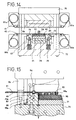
- FIGs. 14 and 15 Another embodiment of the resin molding machine, in which the lower die 21 is vertically moved to mold a semiconductor wafer 90, is shown in Figs. 14 and 15.
- a plurality of pillars 92, to which external terminals will be connected, are vertically formed on an upper face of the semiconductor wafer 90, and the upper face will be molded with resin except upper end faces of the pillars 92. After molding, the semiconductor wafer 90 is divided into a plurality of products.
- the lower die 21 is supported by the movable platen 72, the clamper 76 is biased by the springs 78, and the release film 40 is fed to the lower die 21 as well as the former embodiment.
- the semiconductor wafer 90 is set in the lower die 21 with heading the surface to be molded is upward, and release film 41 is fed to the parting face of the upper die 20.
- the release film 41 prevent the resin from sticking onto the upper die 20.
- the resin molding machine has a feeding roll 81a, which feeds the new release film 41, and a collecting roll 81b, which collects the used release film 41.
- the action of the resin molding machine of the present embodiment will be explained. Firstly, the dies are opened, the release film 41 is fed onto the parting face of the upper die 20, the release film 40 is fed onto the parting face of the lower die 21, and the release film 40 is fixed on the clamper 76 by air suction.
- Resin 94 is set at a center of the semiconductor wafer 90.
- Fig. 14 shows the state in which the resin 94 has been set.
- the movable platen 72 is moved upward so as to clamp. Firstly, the resin 94 is clamped, then the clamper 76 contacts the upper die 20.
- the clamper 76 contacts the upper die 20, and the movable platen is further moved upward, so that the lower die 21 moves the semiconductor wafer 90 upward.
- the upward movement of the semiconductor wafer 90 caused by the lower die 21 is stopped when the stoppers 87 of the lower die 21 contact the stoppers 86 of the upper die 20.
- the resin 94 is melted, and the melted resin 94a fills spaces between the pillars 92. Thickness of the molded product is defined.
- Fig. 15 shows a state in which the lower die 21 is located at the highest position and the stoppers 86 and 87 contact each other.
- the melted resin 94a fills the spaces between the pillars 92, which are vertically provided on the upper face of the semiconductor wafer 90, the upper ends of the pillars 92 slightly bite the release film 41, so that no resin 94a is stuck on the upper end faces of the pillars 92. Even if height of the pillars are slightly different, the difference can be absorbed by the release film 41, so that the upper end faces of the pillars 92 can be exposed after molding.
- the release film 41 is fixed on the parting face of the upper die 20 by sucking air through air sucking holes 96.
- a symbol 98 stands for an overflow cavity.
- Fig. 16 is a plan view of the upper die 20 shown in Fig. 15; Fig. 17 is a plan view of the lower die 21 shown therein.
- a circular pressing face 20c is formed in the parting face of the upper die 20 and capable of pressing the semiconductor wafer 90.
- a plurality of air sucking holes 96 which are capable of fixing the release film 41 on the upper die 20 by air suction, are arranged to enclose the pressing face 20c.
- the air sucking holes 96 are rectangularly arranged, but they may be coaxially circularly arranged with respect to the pressing face 20c.
- the parting faces rounded by the air sucking holes 96 and 76a, which include the inner bottom faces of the cavities, of the dies 20 and 21 are mat-finished by electric discharge machining, sandblast machining, etc., so that fine projections are formed therein.
- the fine projections reduce heat conductivity of the dies, so that the release film is gradually heated and expanded, and the release film can be wholly drawn by air suction. Further, air can be easily introduced outside, so creases of the release film can be gradually removed by continuously sucking air.
- Fine grooves may be formed the parting faces instead of said fine projections.
- Clamping faces of the dies may be formed into smooth flat faces.
- a planar shape of the lower die 21, which supports the semiconductor wafer 90 is a circular shape whose diameter is designed on the basis of that of the semiconductor wafer 90.
- the clamper 76 is capable of slidably moving on an outer circumferential face of the lower die 21.
- a clamping projection 76b is provided on the surface of the clamper 76 and encloses the lower die 21.
- the clamping projection 76b is slightly projected from the parting face so as to securely clamp a border part of a resin-molded part.
- Overflow gates 76c are formed by partially cutting the clamping projection 76b.
- the overflow cavity 98 circularly encloses the clamping projection 76b. Air vents 98a are opened in an inner bottom face of the overflow cavity 98 and communicated with an air mechanism for sucking air so as to draw the release film 40 into the overflow cavity 98. There is formed another overflow cavity 98 in the upper die 20 as well as the lower die 21.
- Sucking grooves 77 are provided, in the lower die 21, on the outer side of the overflow cavity 98.
- four sucking grooves 77 are provided with regular separations.
- Each sucking grooves 77 has air sucking holes 77a, which are opened in an inner bottom face thereof.
- the air sucking holes 77a are also communicated with the air mechanism so as to draw the release film 40 into the sucking grooves 77.
- the sucking grooves 77 may be one circular groove. Note that, if the overflow cavity 98 has a deeper portion therein, the slackened parts of the release film 40 can be drawn thereinto as well as the sucking grooves 77.
- FIG. 18 Another embodiment, in which the surface of the semiconductor wafer 90 on which the pillars 92 are vertically provided is headed downward, is shown in Fig. 18.
- the release film 40 and 41 are respectively fed onto the lower die 21 and the upper die 40, the clamper 76 is provided, and the movable platen 72 supports the lower die 21 as well as the former embodiment.
- a seal ring 101 is provided so as to suck the air through air suckingholes opened in an inner bottom face of the lower die 21.
- the release film 40 and 41 are set on the dies 20 and 21, then the semiconductor wafer 90 is set in the lower die 21 by supporting an outer edge of the semiconductor wafer 90 by an upper face of the clamper 76, and the liquid resin 50 is supplied into a concave section encased by the lower die 21 and the clamper 76.
- Fig. 18 shows the state in which the liquid resin 50 is supplied.
- the outer edge of the semiconductor wafer 90 is clamped between the upper die 20 and the clamper 76 by moving the movable platen 72 upward, then the lower die 21 is further moved upward.
- the upward movement of the lower die 21 is stopped when the stoppers 87 contact the stoppers 86.
- the lower face of the semiconductor wafer 90 including the pillars 92 is wholly soaked into the liquid resin 50.
- the lower die 21 reaches the highest position which defines the thickness of a resin-molded section of the molded product, lower ends of the pillars 92 slightly bite the release film 40, so that no resin will stick onto lower end faces of the pillars 92 and the lower end faces of the pillars 92 can be exposed after completing the molding action.
- the above described methods in which the dies 20 and 21 are covered with the release film 40 and 41 when the surface of the semiconductor wafer 90 including the pillars is molded, can be properly applied to mold one surface of the semiconductor wafer 90 except the end faces of the pillars 92.
- the release film 40 and 41 By covering the parting faces of the dies 20 and 21 with the release film 40 and 41, no resin will stick onto the parting faces, so that a step of cleaning the parting faces is not required. Namely, the molding action can be executed under a clean condition and reliable products can be manufactured.
- the lower die 21 is supported and moved by the movable platen 72, but the member 16 may be clamped by vertically moving the upper die 20 instead of the lower die 21. Namely, the member 16 is clamped by relative movement of the upper die 20 and the lower die 21.
- FIGs. 19A and 19B Another embodiment is shown in Figs. 19A and 19B.
- the clamper 76 has an overflow cavity 102, and the length of the stoppers 86 and 87 can be adjusted.
- the overflow cavity 102 is communicated to the air mechanism via air paths 104.
- a symbol 106 stands for an overflow gate, and a symbol 108 stands for air vents.
- Fig. 19A is a plan view showing the overflow cavity 102, the overflow gate 106 and the air vents 108.
- the overflow cavity 102 is formed like a ring-shaped groove, and the overflow gate 106 is formed on the inner side thereof.
- the air vents 108 are radially outwardly extended from the overflow cavity 102 with regular separations.
- the release film 40 and 41 are clamped by a clamping face 110.
- the resin overflown from the molding section (cavity space) of the die is introduced into the overflow cavity 102, whose inner face is covered with the release film 40.
- Pressure can be applied to the resin in the cavity space by pressurizing the air in the overflow cavity 102 via the air paths 104, so that reducing the resin pressure can be prevented.
- Resistance caused by discharging the resin to the overflow cavity 102 can be controlled by controlling the air pressure in the air paths 104.
- the thickness of the resin-molded section of the molded product can be precisely controlled by amount of the resin discharged into the overflow cavity 102.
- a motor 116 controls the length of the stopper 86 of the upper die 20.
- the stopper 86 is projectably held in a guide rod 86a.
- a oval cam (not shown), which is linked with the stopper 86, is fixed to an output shaft of the motor 116 so as to the projected length of the stopper 86 can be controlled by a rotational position of the oval cam.
- Thickness of the members to be molded are slightly different according to type and lot of the members.
- the thickness of the semiconductor wafers 90 are different according to thickness of protecting layers, length of the pillars 92, etc.. Thus, the difference is absorbed by adjusting the projected length of the stoppers 86.
- the projected length of the stoppers 86 are adjusted about ⁇ 0.1 mm.
- the resin pressure can be effectively applied, so a large die can be employed as the lower die 21.
- degree of resin solidification in a cavity space is partially different.
- the resin solidification begins from a center part of the lower die 21 and gradually advanced toward an outer edge. With this solidification, air in the resin can be introduced outside of the cavity space and forming voids in the molded product can be prevented.
- heat capacity of the center part of the die is greater than that of the outer edge part, or carolific power of the heaters in the center part of the die is greater than that of the heaters in the outer edge part. Note that, heat distribution of the die can be uniform by forming the die into a circular shape.
- heat insulating spaces 108 are formed in the upper die 20 so as to control distribution of the heat capacity in the upper die 20.
- Resin is shrieked while solidification, so the center part of the die may be overfilled so as to make the molded product have predetermined thickness after solidification.
- the center part of the bottom parting face of the upper die is pushed upward and slightly deformed.
- the deformed center part of the upper die 20 returns to the initial state.
- the small gap "G" the upper die 20 can be slightly deformed by the resin pressure.
- the main characteristic point of the resin molding machine of the present invention is using the release film.
- the release film By using the release film, the resin in each cavity space is properly pressurized by air pressure of the air left in the cavity space and the elasticity of the release film.
- Fig. 21 shows a state in which the member 16 to be molded is clamped by the upper die 20 and the lower die 21 together with the release film 40. Since the cavities 26a are respectively divided by the parting sections 28, the air sealed up in each cavity 26a is compressed by clamping the member 16 together with the release film 40. The air sealed up in the cavity 26 and the release film 40 press the resin 34a or 50. This pressing action applies proper pressure to the resin in the cavity space when the resin is solidified and its volume is reduced.
- air paths 33 are formed in the lower die 21 and opened in the inner bottom faces of the cavities 26a, and compressed air is sent through the air paths 33 so as to apply pressure.
- the air pressure may be applied through the air sucking holes 32, which are opened in the inner bottom faces of the cavities 26a so as to fix the release film thereon, instead of the air paths 33.
- runner paths 29 and 29a are formed in the parting sections 28 for dividing the cavities 26a.
- each runner path 29a which communicates the adjacent cavities 26a, is formed in a mid portion of the parting section 28, which is formed between the adjacent cavities 26a; each runner path 29, which diagonally communicates the cavities 26a, is formed in a cross portion of the parting sections 28.
- the method of the present invention can be applied to mold many kinds of members to be molded, e.g., a substrate on which semiconductor chips are mounted, a circuit module including a plastic substrate and circuits elements mounted thereon, a semiconductor wafer, a semiconductor wafer on which electric terminals or circuits are formed.
- the substrate may be a multi-layered substrate, a tape substrate, etc..
- the release film is formed like long sheet and wounded on the feeding roll, but strip-formed release film may be used.
- the resin molding machine can be commonly and efficiently used.
- the parting faces, which include the molding sections, of the upper die 20 and the lower die 21 may be coated with nickel-boron-tungsten alloy by electroless plating. Resin is easily peelable from the coated faces, and resin leakage can be prevented. Further, the parting faces may be coated with a silicic material, fluoric resin or dispersion coating dispersed with oligomer so as to effectively prevent the resin leakage because a moving range of resin in molding dies, one of which is moved to mold.
Abstract
Description
- The present invention relates to a method of manufacturing semiconductor devices and a resin molding machine for said method.
- A conventional method of manufacturing semiconductor devices will be explained with reference to Fig. 24. A plurality of
semiconductor chips 10 are matrically arranged on asubstrate 12 at regular separations. Thesubstrate 12 is molded withresin 14. After theresin 14 is solidified, thesemiconductor chips 10 are respectively separated by cutting theresin 14 and thesubstrate 12 with a dicing cutter or a laser means, so that pieces of the semiconductor devices can be manufactured. - In the conventional method, a large number of
semiconductor chips 10 can be arranged in thesubstrate 12 with high density, so that small semiconductor devices can be efficiently manufactured and manufacturing cost can be effectively reduced. - However, the conventional method, in which one side face of the
substrate 12, on which thesemiconductor devices 10 are arranged, is molded and thesubstrate 12 is cut to form the pieces of the semiconductor devices, has following disadvantages. In the case of cutting thesubstrate 12 with the dicing cutter, a dicing blade of the dicing cutter is apt to be damaged because the dicing blade cuts different materials, i.e., thesubstrate 12 and thesolidified resin 14. Further, edges of the pieces of the semiconductor devices are apt to be broken and cracked. On the other hand, in the case of cutting with the laser means, it takes a long time to cut thesubstrate 12. - If the
semiconductor chips 10 are molded bypotting resin 14, it takes a long time to solidify theresin 14, so manufacturing efficiency is quite low. In the case of molding a transfer molding machine, wires are apt to be deformed by resin flow, so that bad products will be produced. Further, the molded substrate will be deformed of curved because one side face of thesubstrate 12 is wholly molded. - The present invention has been invented to solve the disadvantages of the conventional methods.
- An object of the present invention is to provide a method of manufacturing semiconductor devices, which is capable of efficiently manufacturing semiconductor devices and preventing production of bad products.
- Another object of the present invention is to provide a resin molding machine for executing the method.
- To achieve the objects, the present invention has following basic structures.
- The method of manufacturing semiconductor devices in a molding machine including an upper die and a lower die, in one of which a plurality of cavities corresponding to resin-molded parts of the semiconductor devices are formed,
comprises the steps of: - covering inner faces of the cavities and a parting face of one of the dies, which contacts a substrate of the semiconductor devices, with release film, which is easily peelable from the dies and resin for molding;
- clamping the substrate with the dies;
- filling the resin in the cavities; and
- forming the semiconductor devices by cutting the molded substrate.
-
- And, the method of manufacturing semiconductor devices in a molding machine including an upper die and a lower die,
comprises the steps of: - covering parts of parting faces of the dies, which are capable of clamping a semiconductor wafer, with release film, which is easily peelable from the dies and resin for molding;
- providing the resin onto one side face of the semiconductor wafer;
- clamping the semiconductor wafer by the dies together with the release film so as to mold the one side face of the semiconductor wafer; and
- forming the semiconductor devices by cutting the molded semiconductor wafer.
-
- The resin molding machine,
comprises: - an upper die and a lower die for clamping a member to be molded, which includes a substrate on which semiconductor chips and/or circuit elements are mounted;
- a plurality of cavities being formed in one of the dies, the cavities being capable of accommodating the semiconductor chips and/or the circuit elements;
- a release film feeding mechanism for feeding release film, which is easily peelable from the dies and resin for molding, so as to cover inner faces of the cavities and a parting face of one of the dies, which contacts the substrate; and
- a resin filling mechanism for sending the resin from a pot to the cavities while the member to be molded is clamped by the dies together with the release film,
- whereby the semiconductor chips and/or the circuit elements are respectively molded with resin.
-
- The resin molding machine,
comprises: - an upper die and a lower die for clamping a member to be molded, which includes a substrate on which semiconductor chips and/or circuit elements are mounted;
- a plurality of cavities being formed in the lower die, the cavities being capable of accommodating the semiconductor chips and/or the circuit elements; and
- a release film feeding mechanism for feeding release film, which is easily peelable from the dies and resin for molding, so as to cover inner faces of the cavities and a parting face of the lower die, which contacts the substrate,
- wherein the member to be molded is clamped by the dies together with the release film and molded with the resin which is supplied into a space enclosed with the release film.
-
- And, the resin molding machine for molding a whole one side face of a semiconductor wafer,
comprises: - an upper die and a lower die for clamping a semiconductor wafer;
- a molding section being formed in a parting face of one of the dies; and
- a release film feeding mechanism for feeding release film, which is easily peelable from the dies and resin for molding, so as to cover the parting faces of the dies,
- wherein the semiconductor wafer is clamped by the dies together with the release film and molded with the resin which is supplied into the molding section.
-
- In the method of the present invention, one side face of the substrate, on which a plurality of the semiconductor chips, or the semiconductor wafer can be easily and securely molded with resin. By using the release film, structures of the dies can be simple, no resin flash is formed, and highly reliable semiconductor devices can be manufactured.
- In the resign molding machine of the present invention, the resin-molded parts of the member to be molded can be easily and securely molded with resin. One side of the semiconductor wafer, etc. can be properly molded.
- Embodiments of the present invention will now be described by way of examples and with reference to the accompanying drawings, in which:
- Fig. 1 is a sectional view of a resin molding machine of an embodiment of the present invention wherein a member to be molded is set therein;
- Fig. 2 is a sectional view of the resin molding machine wherein the member to be molded is clamped and molded with resin;
- Fig. 3 is a perspective view of a lower die of the resin molding machine;
- Fig. 4 is a perspective view of the member molded with the resin;
- Fig. 5 is a sectional view of the resin molding machine of another embodiment;
- Fig. 6 is a sectional view of the resin molding machine of another embodiment;
- Fig. 7 is a sectional view of the resin molding machine of another embodiment;
- Fig. 8 is a perspective view of a member molded with resin;
- Fig. 9 is a perspective view of a lower die;
- Fig. 10 is a sectional view of a resin molding machine in which a lower die is capable of moving upwardly to mold with resin;
- Fig. 11 is a sectional view of a state in which a member to be molded is molded with resin;
- Fig. 12 is a sectional view of a resin molding machine in which a lower die is capable of moving upwardly to mold with resin;
- Fig. 13 is an explanation view of a resin molding machine in which a lower die is capable of moving upwardly to mold with resin;
- Fig. 14 is an explanation view of a resin molding machine in which a semiconductor wafer is molded;
- Fig. 15 is an enlarged sectional view of the semiconductor wafer molded with resin;
- Fig. 16 is a plan view of an upper die of the resin molding machine;
- Fig. 17 is a plan view of a lower die of the resin molding machine;
- Fig. 18 is an explanation view of a resin molding machine in which a semiconductor wafer is molded;
- Fig. 19A is a sectional view showing a clamper of the resin molding machine;
- Fig. 19B is a partial plan view of the clamper;
- Fig. 20 is an explanation view showing an inner structure of an upper die;
- Fig. 21 is a sectional view of cavities in which resin is filled;
- Fig. 22 is a sectional view showing runner paths;
- Fig. 23 is a plan view showing the runner paths; and
- Fig. 24 is a sectional view of a molded product, in which semiconductor chips are mounted on a substrate and molded with resin.
-
- Preferred embodiments of the present invention will now be described in detail with reference to the accompanying drawings.
- A resin molding machine of an embodiment of the present invention will be explained with reference to Figs. 1 and 2.
- A plurality of
semiconductor chips 10 are mounted on eachmember 16 to be molded. In eachmember 16, the semiconductor chips 10 are matrically arranged, on asubstrate 12, with regular separations. In the present embodiment, a plurality of multi-chip modules, each of which includes a couple ofsemiconductor chips 10, are produced from themember 16 as semiconductor devices. The method of the present embodiment can be, of course, applied to semiconductor devices, each of which includes onesemiconductor chip 10, threesemiconductor chips 10 or more, or circuit elements, e.g., resistance. - The
members 16 are clamped by anupper die 20 and lower dies 21, and resin is sent from apot 24 tocavity spaces 26 to mold themembers 16. The melted resin is pressurized by aplunger 22. - In the present embodiment,
cavities 26a are formed in the lower dies 21, a side face of eachmember 16, on which the semiconductor chips 10 are mounted, is headed downwardly, then themembers 16 are set in the lower dies 21. Note that, in the case of forming the cavities in theupper die 20, the side faces of themembers 16, on which the semiconductor chips 10 are mounted, is headed upward. - A perspective view of the
lower die 21 is shown in Fig. 3. Thecavities 26a of thelower die 21 are arranged to correspond to the arrangement of the semiconductor chips 10 in thesubstrate 12. Theadjacent cavities 26a are divided by partingsections 28. In the present embodiment, theparting sections 28 are formed like a latticework to divide therectangular cavities 26a. Upper faces of theparting sections 28 are located at the same level, and they act as parts of a parting face of the die. -
Runner paths 30 respectively communicate theadjacent cavity spaces 26. Eachrunner path 30 is formed by partially cutting theparting section 28, so that theadjacent cavity spaces 26 can be communicated via therunner path 30. In the present embodiment, threecavities 26a are serially arranged in the longitudinal direction of the die, and they are communicated by therunner paths 30. - Fig. 1 is the sectional view in which the lower dies 21 are cut a plane passing the
runner paths 30. - In the present embodiment, the
menbers 16 are clamped by theupper die 20 and the lower dies 21. The characteristic point is that the parting faces of the lower dies 21, which include inner faces of thecavities 26a, are covered withrelease film 40, so that no resin directly contacts the parting faces while resin molding is executed. Therelease film 40 has enough heat-resistibility against heat generated from the dies and is easily peelable from the dies. For example, therelease film 40 may be made from PTFE, ETFE, PET, FEP, etc.. Therelease film 40 should have enough flexibility and extensibility so as to easily deform along inner faces of the molding sections, e.g., thecavities 26a. Further, therelease film 40 should be easily peelable from solidified resin. - In the present embodiment, the lower dies 21 are respectively located on each side of the
pot 24. Fig. 1 mainly shows onelower die 21. Of course, thelower die 21 may be located on only one side of thepot 24. Size of the lower dies 21 and number of thecavities 26a of eachlower die 21 may be designed according to themembers 16, etc.. - In Fig. 1, the dies are opened, and the
release film 40 is set to cover the lower dies 21 and thepot 24. As shown in the drawing, therelease film 40 covers an inner circumferential face of thepot 24 and the whole parting faces of the lower dies 21. - The
release film 40 is fed to wholly cover the parting faces, and the feeding action is synchronized with the molding action. Therelease film 40 may be merely mounted on the parting faces of the dies, preferably therelease film 40 is fixed on and along the inner faces of thecavities 26a by sucking air through inner bottom faces of thecavities 26a. Air is sucked throughair sucking holes 32 to fix therelease film 40. Theair sucking holes 32 are formed like, for example, slits and opened in the inner bottom faces of thecavities 26a. Theair sucking holes 32 are communicated to an air mechanism for sucking air. - Since the
release film 40 has enough flexibility, therelease film 40 can be easily deformed and fixed along the inner faces of thecavities 26a by sucking air through the air sucking holes 32. With this action, thecavity spaces 26 for accommodating the semiconductor chips 10 can be formed. - In the
pot 24 too, air is sucked through thepot 24, therelease film 40 is fixed on the inner circumferential face of thepot 24 and an upper end face of theplunger 22. - To fix the
release film 40 in thepot 24, air paths may be formed between the inner circumferential face of thepot 24 and an outer circumferential face of theplunger 22, and the air can be downwardly sucked therethrough. And, air sucking grooves may be vertically formed in the outer circumferential face of theplunger 22, and the air can be sucked therethrough. Since the inner faces of thepot 24 are covered with therelease film 40, no resin will be stuck onto the inner faces of thepot 24. - After the
release film 40 is fixed on the parting face of the lower dies 21 and the inner faces of thepot 24 by air suction, aresin tablet 34 is supplied into thepot 24 and themembers 16 are set in prescribed positions in the lower dies 21. The resin supplied into thepot 24 may be not only the resin tablet but also resin pellets, resin powders, liquid resin, sheet-formed resin, jelly-formed resin, etc.. And, the resin may be thermosetting resin and thermoplastic resin. - Next, the
members 16 are clamped between theupper die 20 and the lower dies 21, and theresin 34a, which is melted in thepot 24, is pressurized and sent by theplunger 22 so that thecavity spaces 26 are filled with theresin 34a. Fig. 2 shows the state in which thecavity spaces 26 are filled with theresin 34a. Firstly, thecavity space 26 which is the nearest to thepot 24 is filled with theresin 34a, then furthercavity spaces 26 are filled in order. Eachrunner path 30 mutually, communicates theadjacent cavity spaces 26 and acts as a resin path to fill thecavity spaces 26 with theresin 34a. After theresin 34a is sent from thepot 24 to all thecavity spaces 26, resin pressure is kept to solidify theresin 34a. - After the
resin 34a is solidified, the dies are opened, and the molded products are taken from the lower dies 21. The molded products may be taken out by the steps of: taking out the molded products, together with therelease film 40, from the dies; and removing therelease film 40 from the molded products, or by the steps of: removing the release film from the molded products in the dies; and separately taking out the molded products and therelease film 40 from the dies. - The molded member (product) is shown in Fig. 4. A plurality of rectangular resin-molded
sections 36 are matrically arranged on thesubstrate 12 with regular separations. No resin is stuck between the adjacent resin-moldedsections 36, so that the surface of thesubstrate 12 is partially exposed therebetween.Resin pieces 30a were solidified in therunner paths 30 and stuck to thesubstrate 12. - The semiconductor devices are completed by dividing the
substrate 12 along the resin-moldedsections 36. In Fig. 4, lines A-A are dividing lines in the longitudinal direction of thesubstrate 12; lines B-B are dividing lines perpendicular to the dividing lines A-A. In the products molded by the resin molding machine of the present embodiment, the solidifiedresin pieces 30a are partially left in therunner paths 30, but the surface of the substrate is partially exposed between the adjacent resin-moldedsections 36 so that pieces of the semiconductor devices can be easily gained by cutting thesubstrate 12 along the dividing lines. - Since the semiconductor devices are separated by cutting the
substrate 12 only, a blade of a dicing cutter is not damaged and the semiconductor devices can be easily separated. To easily cut thesubstrate 12 by the dicing cutter, slit holes may be formed along the dividing lines except the portions in which therunner paths 30 are formed. - Further, notches, which corresponds to the dividing lines, may be formed in the
substrate 12. In this case, thesubstrate 12 is broken along lines including the notches so as to separate the semiconductor devices. - By employing the
release film 40, themembers 16 to be molded can be securely clamped and properly molded. If thesubstrate 12 is made of a plastic, thickness of thesubstrate 12 is partially different. But, the difference of the thickness can be absorbed by therelease film 40, so that thesubstrate 12 can be securely molded without forming resin flash on the surface thereof. - In the conventional resin molding machine, the molded products are ejected by ejector pins while the dies are opened. By employing the
release film 40, the molded products can be ejected from the dies without ejector pins. Namely, no ejector pins are assembled in the dies, so that structures of the dies can be simpler. - By covering the inner faces of the molding sections, e.g., the cavities, with the
release film 40, theresin 34a can smoothly flow on inner faces of thecavities 26a, so that thecavity spaces 26 can be easily filled with theresin 34 and the substrates can be securely molded without forming voids in the resin-moldedsections 36. Since theresin 34a can smoothly flow in thecavity spaces 26, semiconductor devices having thin resin-moldedsections 36, whose thickness is, for example, 0.1 mm, can be manufactured easily. - In the conventional resin molding machine, the resin, which is capable of smoothly flowing in the
cavity spaces 26 and easily peelable from the dies, is selected. In the present embodiment, since therelease film 40 is employed, the resin does not directly contact the dies, so that the resin may be selected on the basis of characteristics of filling thecavity spaces 26 and electric characteristics of the semiconductor devices only. - The
release film 40 may be used as shown in Fig. 5. Two sheets of therelease film 40 respectively cover the parting faces of theupper die 20 and thelower die 21. And, thepot 24 may be faced to the substrate of themember 16. - Further, as shown in Fig. 6,
concave sections 20a, whose depth is equal to the thickness of themember 16 to be molded, may be formed in theupper die 20 so as to accommodate themembers 16 respectively therein. - In the present embodiment, the
runner paths 30 are formed in theparting sections 28 of the lower dies 21. To leave no solidified resin pieces, which have been solidified in therunner paths 30, on thesubstrate 12, the dies shown in Fig. 7 may be employed. - In the dies shown in Fig. 7, the
parting sections 28a divide therectangular cavities 26a as well as theparting sections 28 of thelower die 21 shown in Fig. 3. But, theparting sections 28a of Fig. 7 are parting plates, which can be moved in the vertical direction. Theparting plates 28a are supported by a supportingplate 38, which is moved in the vertical direction. - In Fig. 7, the
members 16 are clamped by theupper die 20 and the lower dies 21 together with therelease film 40, and theresin 34a is sent from thepot 24 to thecavity spaces 26. Since upper end faces of theparting plates 28a are separated from the bottom face of thesubstrate 12 so as to form theresin paths 31, which mutually communicate theadjacent cavity spaces 26, when thecavity spaces 26 are filled with theresin 34a, all thecavity spaces 26 can be filled with theresin 34a. Upon filling all thecavity spaces 26 with theresin 34a, the supportingplate 38 is moved upward until the upper end faces of theparting plates 28a contact the bottom face of thesubstrate 12, so that eachcavity space 26 can be perfectly divided. - With this manner, no resin pieces are left in the
resin paths 31, each of which is formed on the bottom face of thesubstrate 12 and communicates theadjacent cavity spaces 26, after completing the molding action, so that the molded product whose resin-moldedsections 36 are perfectly separated on thesubstrate 12 can be produced as shown in Fig. 8. Since the resin-moldedsections 36 are perfectly separated, the pieces of the semiconductor devices can be easily produced by cutting thesubstrate 12. - The
parting plates 28a is moved in vertical holes bored in the lower dies 21, so therelease film 40 can be fixed on and along the inner faces of thecavities 26a by sucking air through the vertical holes. Therefore, no air sucking holes are separately required. - In the above described embodiments, the
cavities 26a are formed in the lower dies 21, but the methods can be applied to the resin molding machine in which thecavities 26a are formed in theupper die 20. In the case of forming thecavities 26a in theupper die 20, the resin paths for mutually communicating thecavity spaces 26 are formed in theupper die 20. - A molding die in which the
cavities 26a are perfectly divided by theparting sections 28 is shown in Fig. 9. In the above described embodiments, theadjacent cavity spaces 26 are mutually communicated by forming therunner paths 30 in theparting sections 28 or moving theparting plates 28a downward. The member to be molded can be molded by the die 21 shown in Fig. 9, in which thecavities 26a are divided by the fixedparting sections 28 which have norunner paths 30. - Fig. 10 shows another embodiment in which the
lower die 21 has fixedparting sections 28 having norunner paths 30 and the resin is liquid resin. Alower base 42 guides an open-close movement of thelower die 21. A supportingrod 44 is connected to a driving mechanism (not shown) for moving thelower die 21 in the open-close direction. For example, the driving mechanism has a ball bearing screw for moving the supportingrod 44, and a motor for rotating the ball bearing screw, so that thelower die 21 can be linearly moved in the open-close direction. - As shown in Fig. 10, the open-close direction of the
lower die 21 is slightly inclined with respect to the vertical line VL, theliquid resin 50 is supplied in a state that therelease film 40 is not fixed onto the molding sections of thelower die 21 by air suction, then themember 16 to be molded is clamped and molded. Note that, an angle shown in Fig. 10 is an inclination angle of the dies with respect to the vertical line VL. - The
release film 40 is fed when the dies are opened, and edges of therelease film 40 are supported by thelower base 42, then theliquid resin 50 having prescribed volume is supplied onto therelease film 40. Fig. 10 shows a state of clamping edges of themember 16 by theupper die 20 and thelower base 42. Therelease film 40 is slackened, and theliquid resin 50 is gathered on therelease film 40. Since the dies are inclined, theliquid resin 50 is gathered aside to the left side of a center line CL. - The
liquid resin 50 has enough volume to fully fill all the cavities formed in the lower dies 21. - In Fig. 10, the
lower die 21 is located at the lower end position. Theliquid resin 50 is pressed upward, together with therelease film 40, by the upward movement of thelower die 21. Since the dies are inclined, firstly thelowest cavity space 26 is filled with theliquid resin 50 thenhigher cavity spaces 26 are filled in order. - A state that the
lower die 21 is located at the upper end position and themember 16 is clamped by theupper die 20 and thelower die 21 is shown in Fig. 11. All thecavity spaces 26 are covered with therelease film 40 and filled with theliquid resin 50. Themember 16 is molded by solidifying theliquid resin 50 in the state of clamping themember 16 by theupper die 20 and thelower die 21.Heaters 46 heat theupper die 20 and thelower die 21. - The
lower die 21 has theparting sections 28, which are formed like a latticework, but the dies are inclined and theliquid resin 50 is introduced into thecavity spaces 26, from the lowest cavity space to the higher cavity spaces in order, so that all thecavity spaces 26 can be filled with theliquid resin 50 without forming therunner paths 30 in theparting sections 28. Without forming therunner paths 30 in theparting sections 28, the independent resin-moldedsections 36 can be formed on themember 16 as shown in Fig. 8. - In the case of employing the
liquid resin 50, the volume of theliquid resin 50 is slightly greater than total volume of thecavity spaces 26 to be filled with theliquid resin 50. Anoverflow cavity 48, into which theliquid resin 50 which has overflown is collected, is formed in a parting face of thelower base 42. Theoverflow cavity 48 is formed in the parting face of thelower base 42 and located adjacent to the highest cavity of thelower die 21. The cavity spaces are filled from the lowest cavity space to the higher ones, so theliquid resin 50 finally overflows from the highest cavity space and collected into theoverflow cavity 48. - Note that, a resin tablet may be used instead of the
liquid resin 50. In this case, the molding action is executed by the steps of: supporting therelease film 40 by thelower base 42; supplying the resin tablet onto therelease film 40; melting the resin tablet by the heat of the dies; and moving thelower die 21 upward. With this steps, the resin melted is gradually supplied into the cavity spaces, so that themember 16 is molded as well as the case of using theliquid resin 50. - If the resin tablet which forms few voids is used, good resin-molded sections having few voids can be formed as well as the
liquid resin 50. - In the resin molding machines shown in Figs. 10-12, the parting face of the
lower die 21 is parallel to that of theupper die 20. For example, level difference between the lowest point of the parting face of thelower die 21 and the highest point thereof, which is caused by inclining the dies, is 0.05 mm, so themember 16 can be gradually clamped from the lowest edge to the highest edge. With this action, the air in the cavity spaces is easily introduced out from the highest side, and therelease film 40 is slightly pulled and extended toward the higher side when therelease film 40 is clamped, so that no crease is formed in therelease film 40. - Another embodiment of the resin molding machine, whose dies are inclined and whose lower die is moved upward and downward, is shown in Fig. 12. A
melting section 60, in which theresin tablet 34 is melted, is provided to theupper die 20 or thelower die 21 as a resin supplying section. The meltedresin 34a, which has been melted in themelting section 60, is supplied onto therelease film 40. As shown in Fig. 12, themelting section 60 is provided to theupper die 20 and has aplate 62 for pressing theresin tablet 34 and aspring 64 for biasing theplate 62. Theresin tablet 34 is pressed by theplate 62 and heated, so that theresin tablet 24 is melted. Asymbol 66 stands for a heater. - The dies 20 and 21 are inclined as well as the former embodiment, so the
melting section 60 is provided to the higher side of theupper die 21. The meltedresin 34a, which has been melted in themelting section 60, is pressed and sent to an upper face of therelease film 40 by theplate 62. Agate 68 introduces theresin 34a from a base portion of themelting section 60 to thelower die 21. - The action of the resin molding machine will be explained. The
release film 40 and themember 16 to be molded are set while the dies are opened, theresin tablet 34 is supplied into themelting section 60, then theupper die 20 and thelower base 42 are closed. Next, the dies are inclined as shown in Fig. 12 so as to supply the meltedresin 34a onto therelease film 40. The meltedresin 34a may be supplied other ways instead of themelting section 60 of theupper die 20. For example, the resin tablet may be supplied into a pot, which is provided in thelower die 21, and the meltedresin 34a is sent, by a plunger, from the pot via thegate 68. Resin pellets and liquid resin may be used instead of the resin tablet. The liquid resin may be tightly wrapped with plastic film and formed like a tablet or a pencil. - In the present embodiment, the
lower die 21 is the movable die, and themember 16 is clamped by moving thelower die 21 upward. But functions of the dies 20 and 21 may be changed. For example, theupper die 20 may be the movable die, thecavities 26a may be formed in theupper die 20, and the semiconductor chips 10 of themember 16 may be headed upward to be molded. In the present embodiment, the meltedresin 34a is supplied into thecavity spaces 26 by themelting section 60 or the pot-plunger mechanism. The parting face of theupper die 20 may be covered with therelease film 40 too so as to execute the molding action without sticking the solidified resin onto the parting face of the upper die. - In the resin molding machines shown in Figs. 10-12, the plate-shaped lower die 21, in which the
cavities 26a are formed, is moved upward to mold themember 16 without pressurizing and sending the resin from the pot to the cavity spaces. - Another embodiment, in which the
lower die 21 is capable of vertically moving, is shown in Fig. 13. - In Fig. 13, the
upper die 20 is fixed to a fixedplaten 70; thelower die 21 is fixed to amovable platen 72 so as to vertically move thelower die 21. In the embodiments shown in Figs. 10-12, the lower dies 21 are inclined with respect to the vertical line. In the present embodiment, thelower die 21 is moved in the vertical direction. Thelower die 21 is fixed to thelower base 42 with abase block 74, and thelower base 42 is fixed to themovable platen 72. With this structure, thelower die 21 is moved by themovable platen 72. -
Clampers 76 clamp outer edges of themember 16. Theclampers 76 are always biased toward theupper die 20 bysprings 78 and capable of vertically moving with respect to themovable platen 72. Note that, theclampers 76 may be biased by other means, e.g., air cylinder units. In the case of employing the air cylinder units, upper end faces of theclampers 76 are coincided with inner bottom faces of thecavities 26 when themember 16 is set in thelower die 21, so that themember 16 can be set on a flatter surface. With this structure, especially in the case of molding large members, e.g., semiconductor wafers, breaking themembers 16 can be prevented. - There are provided a
feeding roll 80a, which feeds thenew release film 40, and a collectingroll 80b, which collects the usedrelease film 40, in the resin molding machine. Therelease film 40 is intermittently fed from the feedingroll 80a to thelower die 21 and wound around the collectingroll 80b with the molding steps of the machine. Afeed roller 82 feeds therelease film 40; acollect roller 84 pulls therelease film 40. - The action of the resin molding machine will be explained.
- Firstly, the
lower die 21 is located at the lowest position, and thenew release film 40 is fed onto thelower die 21. When thelower die 21 is located at the lowest position, the upper end (clamping) faces of theclampers 76 are upwardly projected from the parting face of thelower die 21 by the elasticity of thesprings 78. Therelease film 40 covers over the upper end faces of theclampers 76 and is fixed thereon by sucking air throughair sucking holes 76a, which are respectively formed in theclampers 76. - Next, air is sucked through air sucking holes, which are opened an inner bottom face of the
lower die 21, so that a resin reservoir section, which is encased by thelower die 21 and theclampers 76, in therelease film 40. Theliquid resin 50 is supplied into the resin reservoir section. - A plurality of the semiconductor chips 10 are mounted on a bottom face of the
substrate 12 of themember 16. Themember 16 is correctly set on theupper die 20 or theclampers 76 which have been covered with therelease film 40. - After the
member 16 is set, themovable platen 72 is moved upward so as to clamp themember 16 by theupper die 20, theclampers 76 and thelower die 21. When themovable platen 72 is moved upward, firstly the outer edges of themember 16 are clamped by theclampers 76 and theupper die 20, then themovable platen 72 is further moved upward, so that themember 16 is clamped by theupper die 20 and thelower die 21. After the movement of theclampers 76 are stopped, thesprings 78 are compressed while thelower die 21 is moved upward. -
Stoppers lower die 21. Thelower die 21 is capable of upwardly moving until end faces of thestoppers 87 contact end faces of thestoppers 86. Thestoppers member 16 by themovable platen 72. - In the state of clamping the outer edges of the
member 16, wires, the semiconductor chips 10 and thesubstrate 12 are soaked into theliquid resin 50 in order by moving thelower die 21 upward. With soaking them into theliquid resin 50, theliquid resin 50 pushes therelease film 40 and fills thecavity spaces 26, so that the wires and the semiconductor chips 10 are molded with the resin. - When the
lower die 21 reaches the highest position, theliquid resin 50 is heated to solidify. Theupper die 20 and thelower die 20 have been heated by theheaters 46. - After the resin is solidified, the
movable platen 72 is moved downward so as to open the dies. When the dies are opened, firstly thelower die 21 is moved downward with clamping the moldedmember 16 by theclampers 76, then theclampers 76 are moved downward with supporting the moldedmember 16. Upon fully opening the dies, the moldedmember 16 is taken out from the die, the air suction is stopped to release therelease film 40 from theclampers 76, then thenew release film 40 is fed. The resin molding machine is ready to mold the next member to be molded. - In the present embodiment, the plate-shaped lower die 21, which includes a plurality of the
cavities 26a, is moved by themovable platen 72, so resin pressure effectively works to themember 16. Thus, in comparison with a transfer resin molding machine, a small-powered press mechanism can be employed. In the conventional transfer resin molding machine, the output power of the press mechanism is about 120 ton, and thrust force of a plunger is about 3 ton; in the resin molding machine of the present embodiment, required output power of the press mechanism is about 15 ton. - The resin molding machine of the present embodiment is capable of molding large sized plate members, e.g., A3, A4, with the resin. The
heaters 46 are assembled in theupper die 20 and thelower die 21, themembers 16 are heated from the both side faces so as to accelerate the solidification of the resin, so that working efficiency of the molding action can be improved. Note that, preferably calorific power of the heaters which locate center parts of the dies are greater than others, so that the resin can be solidified from a center and deformation of the molded member can be prevented. If a heater is provided to a loader, which sets themember 16 in the die, so as to preheat themember 16, the deformation of the moldedmember 16 can be further prevented. - In the present embodiment, the
member 16 is clamped between the dies 20 and 21 by vertically moving thelower die 21, the deformation of the wires connected to the semiconductor chips can be prevented, so that reliable molding can be executed. Further, no stress is stored in the solidified resin, so that the deformation of the molded membercan be prevented. - Since the resin molding is executed with using the
release film 40, borders of thecavities 26 can securely clamp thesubstrate 12 even if the thickness of thesubstrate 12 is partially different, so that no resin flash is formed on the surface of thesubstrate 12. By covering thelower die 21 with therelease film 40, no resin is stuck onto thelower die 21 and theclampers 76 and invades into movable parts of mechanisms, so that the movable parts can move smoothly. - Another embodiment of the resin molding machine, in which the
lower die 21 is vertically moved to mold asemiconductor wafer 90, is shown in Figs. 14 and 15. - A plurality of
pillars 92, to which external terminals will be connected, are vertically formed on an upper face of thesemiconductor wafer 90, and the upper face will be molded with resin except upper end faces of thepillars 92. After molding, thesemiconductor wafer 90 is divided into a plurality of products. - As shown in Fig. 14, the
lower die 21 is supported by themovable platen 72, theclamper 76 is biased by thesprings 78, and therelease film 40 is fed to thelower die 21 as well as the former embodiment. However, in the present embodiment, thesemiconductor wafer 90 is set in thelower die 21 with heading the surface to be molded is upward, andrelease film 41 is fed to the parting face of theupper die 20. Therelease film 41 prevent the resin from sticking onto theupper die 20. The resin molding machine has afeeding roll 81a, which feeds thenew release film 41, and a collectingroll 81b, which collects the usedrelease film 41. - The action of the resin molding machine of the present embodiment will be explained. Firstly, the dies are opened, the
release film 41 is fed onto the parting face of theupper die 20, therelease film 40 is fed onto the parting face of thelower die 21, and therelease film 40 is fixed on theclamper 76 by air suction. - Next, air is sucked through the air sucking holes, which are opened an inner bottom face of the
lower die 21, so that a concave section, which is encased by thelower die 21 and theclamper 76, in therelease film 40. Thesemiconductor wafer 90 is set in the concave section. -
Resin 94 is set at a center of thesemiconductor wafer 90. Fig. 14 shows the state in which theresin 94 has been set. - Then, the
movable platen 72 is moved upward so as to clamp. Firstly, theresin 94 is clamped, then theclamper 76 contacts theupper die 20. - The
clamper 76 contacts theupper die 20, and the movable platen is further moved upward, so that thelower die 21 moves thesemiconductor wafer 90 upward. The upward movement of thesemiconductor wafer 90 caused by thelower die 21 is stopped when thestoppers 87 of thelower die 21 contact thestoppers 86 of theupper die 20. In this state, theresin 94 is melted, and the meltedresin 94a fills spaces between thepillars 92. Thickness of the molded product is defined. - When the
lower die 21 is moved upward, theresin 94 is gradually melted, the meltedresin 94a flows from the center to an outer edge of thesemiconductor wafer 90, and finally the meltedresin 94a fill the spaces between thepillars 92. - Fig. 15 shows a state in which the
lower die 21 is located at the highest position and thestoppers resin 94a fills the spaces between thepillars 92, which are vertically provided on the upper face of thesemiconductor wafer 90, the upper ends of thepillars 92 slightly bite therelease film 41, so that noresin 94a is stuck on the upper end faces of thepillars 92. Even if height of the pillars are slightly different, the difference can be absorbed by therelease film 41, so that the upper end faces of thepillars 92 can be exposed after molding. Therelease film 41 is fixed on the parting face of theupper die 20 by sucking air through air sucking holes 96. Asymbol 98 stands for an overflow cavity. - Fig. 16 is a plan view of the
upper die 20 shown in Fig. 15; Fig. 17 is a plan view of thelower die 21 shown therein. In Fig. 16, a circularpressing face 20c is formed in the parting face of theupper die 20 and capable of pressing thesemiconductor wafer 90. A plurality ofair sucking holes 96, which are capable of fixing therelease film 41 on theupper die 20 by air suction, are arranged to enclose thepressing face 20c. Theair sucking holes 96 are rectangularly arranged, but they may be coaxially circularly arranged with respect to thepressing face 20c. - The parting faces rounded by the
air sucking holes - Fine grooves may be formed the parting faces instead of said fine projections. Clamping faces of the dies may be formed into smooth flat faces.
- As shown in Fig. 17, a planar shape of the
lower die 21, which supports thesemiconductor wafer 90, is a circular shape whose diameter is designed on the basis of that of thesemiconductor wafer 90. Theclamper 76 is capable of slidably moving on an outer circumferential face of thelower die 21. A clampingprojection 76b is provided on the surface of theclamper 76 and encloses thelower die 21. The clampingprojection 76b is slightly projected from the parting face so as to securely clamp a border part of a resin-molded part.Overflow gates 76c are formed by partially cutting the clampingprojection 76b. - The
overflow cavity 98 circularly encloses the clampingprojection 76b.Air vents 98a are opened in an inner bottom face of theoverflow cavity 98 and communicated with an air mechanism for sucking air so as to draw therelease film 40 into theoverflow cavity 98. There is formed anotheroverflow cavity 98 in theupper die 20 as well as thelower die 21. - Sucking
grooves 77 are provided, in thelower die 21, on the outer side of theoverflow cavity 98. In the present embodiment, four suckinggrooves 77 are provided with regular separations. Each suckinggrooves 77 hasair sucking holes 77a, which are opened in an inner bottom face thereof. Theair sucking holes 77a are also communicated with the air mechanism so as to draw therelease film 40 into the suckinggrooves 77. By sucking slackened parts of therelease film 40 into the suckinggrooves 77, creases of therelease film 40 can be removed. The suckinggrooves 77 may be one circular groove. Note that, if theoverflow cavity 98 has a deeper portion therein, the slackened parts of therelease film 40 can be drawn thereinto as well as the suckinggrooves 77. - Another embodiment, in which the surface of the
semiconductor wafer 90 on which thepillars 92 are vertically provided is headed downward, is shown in Fig. 18. In the present embodiment, therelease film lower die 21 and theupper die 40, theclamper 76 is provided, and themovable platen 72 supports thelower die 21 as well as the former embodiment. Aseal ring 101 is provided so as to suck the air through air suckingholes opened in an inner bottom face of thelower die 21. - In the present embodiment, the
release film semiconductor wafer 90 is set in thelower die 21 by supporting an outer edge of thesemiconductor wafer 90 by an upper face of theclamper 76, and theliquid resin 50 is supplied into a concave section encased by thelower die 21 and theclamper 76. Fig. 18 shows the state in which theliquid resin 50 is supplied. - Successively, the outer edge of the
semiconductor wafer 90 is clamped between theupper die 20 and theclamper 76 by moving themovable platen 72 upward, then thelower die 21 is further moved upward. The upward movement of thelower die 21 is stopped when thestoppers 87 contact thestoppers 86. With the upward movement of thelower die 21, the lower face of thesemiconductor wafer 90 including thepillars 92 is wholly soaked into theliquid resin 50. When thelower die 21 reaches the highest position which defines the thickness of a resin-molded section of the molded product, lower ends of thepillars 92 slightly bite therelease film 40, so that no resin will stick onto lower end faces of thepillars 92 and the lower end faces of thepillars 92 can be exposed after completing the molding action. - The above described methods, in which the dies 20 and 21 are covered with the
release film semiconductor wafer 90 including the pillars is molded, can be properly applied to mold one surface of thesemiconductor wafer 90 except the end faces of thepillars 92. By covering the parting faces of the dies 20 and 21 with therelease film - In the resin molding machines shown in Figs. 13, 14 and 18, the
lower die 21 is supported and moved by themovable platen 72, but themember 16 may be clamped by vertically moving theupper die 20 instead of thelower die 21. Namely, themember 16 is clamped by relative movement of theupper die 20 and thelower die 21. - Another embodiment is shown in Figs. 19A and 19B. In the resin molding machine, the
clamper 76 has anoverflow cavity 102, and the length of thestoppers - The
overflow cavity 102 is communicated to the air mechanism viaair paths 104. Asymbol 106 stands for an overflow gate, and asymbol 108 stands for air vents. Fig. 19A is a plan view showing theoverflow cavity 102, theoverflow gate 106 and the air vents 108. Theoverflow cavity 102 is formed like a ring-shaped groove, and theoverflow gate 106 is formed on the inner side thereof. The air vents 108 are radially outwardly extended from theoverflow cavity 102 with regular separations. Therelease film face 110. - The resin overflown from the molding section (cavity space) of the die is introduced into the
overflow cavity 102, whose inner face is covered with therelease film 40. Pressure can be applied to the resin in the cavity space by pressurizing the air in theoverflow cavity 102 via theair paths 104, so that reducing the resin pressure can be prevented. Resistance caused by discharging the resin to theoverflow cavity 102 can be controlled by controlling the air pressure in theair paths 104. The thickness of the resin-molded section of the molded product can be precisely controlled by amount of the resin discharged into theoverflow cavity 102. - A
motor 116 controls the length of thestopper 86 of theupper die 20. Thestopper 86 is projectably held in aguide rod 86a. A oval cam (not shown), which is linked with thestopper 86, is fixed to an output shaft of themotor 116 so as to the projected length of thestopper 86 can be controlled by a rotational position of the oval cam. Thickness of the members to be molded are slightly different according to type and lot of the members. For example, the thickness of thesemiconductor wafers 90 are different according to thickness of protecting layers, length of thepillars 92, etc.. Thus, the difference is absorbed by adjusting the projected length of thestoppers 86. In the present embodiment, the projected length of thestoppers 86 are adjusted about ± 0.1 mm. - In the resin molding machine whose
lower die 21 is vertically moved to mold, the resin pressure can be effectively applied, so a large die can be employed as thelower die 21. However, in a large die, degree of resin solidification in a cavity space is partially different. In the case of regarding the lower die as a large cavity, preferably the resin solidification begins from a center part of thelower die 21 and gradually advanced toward an outer edge. With this solidification, air in the resin can be introduced outside of the cavity space and forming voids in the molded product can be prevented. To begin the resin solidification from the center part of thelower die 21, heat capacity of the center part of the die is greater than that of the outer edge part, or carolific power of the heaters in the center part of the die is greater than that of the heaters in the outer edge part. Note that, heat distribution of the die can be uniform by forming the die into a circular shape. - In Fig. 20,
heat insulating spaces 108 are formed in theupper die 20 so as to control distribution of the heat capacity in theupper die 20. - Resin is shrieked while solidification, so the center part of the die may be overfilled so as to make the molded product have predetermined thickness after solidification. When the resin is filled in the cavity space (not shown) in the lower die (not shown) with proper resin pressure, the center part of the bottom parting face of the upper die is pushed upward and slightly deformed. After the resin is solidified, the deformed center part of the
upper die 20 returns to the initial state. In Fig. 20, there is a small gap "G", e.g., 0.02 mm, is formed in theupper die 20. By the small gap "G", theupper die 20 can be slightly deformed by the resin pressure. - As described in the embodiments, the main characteristic point of the resin molding machine of the present invention is using the release film. By using the release film, the resin in each cavity space is properly pressurized by air pressure of the air left in the cavity space and the elasticity of the release film.
- Fig. 21 shows a state in which the
member 16 to be molded is clamped by theupper die 20 and thelower die 21 together with therelease film 40. Since thecavities 26a are respectively divided by theparting sections 28, the air sealed up in eachcavity 26a is compressed by clamping themember 16 together with therelease film 40. The air sealed up in thecavity 26 and therelease film 40 press theresin - In the embodiment shown in Fig. 21,
air paths 33 are formed in thelower die 21 and opened in the inner bottom faces of thecavities 26a, and compressed air is sent through theair paths 33 so as to apply pressure. The air pressure may be applied through theair sucking holes 32, which are opened in the inner bottom faces of thecavities 26a so as to fix the release film thereon, instead of theair paths 33. - In a molding die shown in Figs. 22 and 23,
runner paths parting sections 28 for dividing thecavities 26a. In the present embodiment, eachrunner path 29a, which communicates theadjacent cavities 26a, is formed in a mid portion of theparting section 28, which is formed between theadjacent cavities 26a; eachrunner path 29, which diagonally communicates thecavities 26a, is formed in a cross portion of theparting sections 28. By forming the runner paths, the air left can be introduced from onecavity space 26 to others and the resin pressure in thecavity spaces 26 can be balanced. Further, the runner path is capable of making amount of the resin in thecavity spaces 26 equal as well as therunner paths 30 of the above described embodiment. - The method of the present invention can be applied to mold many kinds of members to be molded, e.g., a substrate on which semiconductor chips are mounted, a circuit module including a plastic substrate and circuits elements mounted thereon, a semiconductor wafer, a semiconductor wafer on which electric terminals or circuits are formed. The substrate may be a multi-layered substrate, a tape substrate, etc..
- In the above described embodiments, the release film is formed like long sheet and wounded on the feeding roll, but strip-formed release film may be used.
- If the sizes of the dies are limited to specific sizes, e.g., A3, A4, A5, the resin molding machine can be commonly and efficiently used.
- The parting faces, which include the molding sections, of the
upper die 20 and thelower die 21 may be coated with nickel-boron-tungsten alloy by electroless plating. Resin is easily peelable from the coated faces, and resin leakage can be prevented. Further, the parting faces may be coated with a silicic material, fluoric resin or dispersion coating dispersed with oligomer so as to effectively prevent the resin leakage because a moving range of resin in molding dies, one of which is moved to mold.
Claims (16)
- A method of manufacturing molded semiconductor devices using a molding machine including an upper die (20) and a lower die (21), comprising the steps of clamping a substrate (12) carrying semiconductor devices (10) to be molded between the dies, filling cavities (26) in one of the dies (20,21) with resin (14), and forming the molded semiconductor devices by cutting the mold substrate (12), characterised in that said cavities (26) are formed in one of said dies (20,21) and are positioned to receive therein at least one semiconductor device (10) to be molded, the method comprising the step of covering inner faces of said cavities (26) and a parting face of one of said dies (20,21) which contacts the substrate (12) carrying the semiconductor devices (10) to be molded with release film (40) which is easily peelable from said dies (20,21) and from said resin (14).
- The method according to claim 1, wherein said cavities (26) are formed in a molding face of said die (21) and are divided by parting sections (28) whose end faces act as a part of the parting face, wherein resin paths (30) are formed in said parting section (28) so as mutually to communicate adjacent cavities (26), and wherein the resin (34a) is pressurised in a pot (24) and sent from the pot (24) to said cavities (26).
- The method according to claim 1, wherein said cavities (26) are formed in a molding face of said die (21) and are divided by a parting plate (28a), which is provided in said die (21) and which is capable of moving in the open-close direction of said dies (20,21).
- The method according to any one of claims 1 to 3 wherein said release film (40) is fixed on the inner faces of said cavities (26) by sucking air through air sucking holes (32), which respectively open into the inner faces of said cavities, when the inner faces of said cavities (26) and the parting face of said die (21) are covered with said release film (40).
- The method according to claim 1, wherein said cavities (26) are formed in a molding face of the lower die (21) and are divided by parting sections (28) whose end faces act as parts of the parting face, wherein said release film (40) is provided to cover over the parting face of said lower die (21) while said dies (20,21) are open, wherein the resin (34a), the volume of which is enough to fill said cavities (26), is fed to, to fill, said cavities (26), the inner faces of which are covered with said release film (40), and wherein the substrate (12) is clamped between the upper die (20) and the lower die (21) together with said release film (40), whereby resin-molded parts divided by said parting sections (28) are respectively molded with the resin (34a).
- The method according to claim 5, wherein the open-close direction of movement of said dies (20,21) is inclined with respect to the vertical.
- The method according to claim 5 or claim 6, wherein resin (34a) is supplied to one of said dies into a space defined by the release film (40).
- A method of manufacturing molded semiconductor devices using a molding machine including an upper die (20) and a lower die (21), comprising the steps of feeding resin (34a) onto one side face of a semiconductor wafer (90); clamping the semiconductor wafer (90) between said dies (20,21), and forming the molded semiconductor devices by cutting the molded semiconductor wafer (90), characterised by the steps of covering parts of parting faces of said dies (20,21) with release film (40), which is easily peelable from said dies (20,21) and from the resin (34a), and clamping the semiconductor wafer (90), together with said release film (40), between said dies (20,21).
- The method according to claim 8, wherein a plurality of pillars (92), to which external terminals are connected, are provided on one side face of the semiconductor wafer (90) to be molded.
- A resin molding machine comprising an upper die (20) and a lower die (21) for clamping therebetween a member (16) to be molded, which member (16) includes a substrate (12) on which semiconductor chips (10) and/or circuit elements are mounted, a plurality of cavities (26) being formed in one of said dies (20,21), said cavities (26) being capable of accommodating the semiconductor chips (10) and/or the circuit elements, characterised by a release film feeding mechanism for feeding release film (40), which is easily peelable from said dies (20,21) and from the resin (34a), so as to cover inner faces of said cavities (26) and a parting face of one of said dies (20,21) which contacts the substrate (12), and a resin filling mechanism for feeding resin (34a) from a pot (24) to said cavities (26) while the member (16) to be molded, together with said release film (40), is clamped between said dies, whereby the semiconductor chips (10) and/or the circuit elements are respectively molded with resin (34a).
- A resin molding machine comprising an upper die (20) and a lower die (21) for clamping therebetween a member (16) to be molded, which member (16) includes a substrate (12) on which semiconductor chips (10) and/or circuit elements are mounted, a plurality of cavities (26) being formed in said lower die (21), said cavities (26) being capable of accommodating the semiconductor chips (10) and/or the circuit elements, characterised by a release film feeding mechanism for feeding release (20,21) and from the resin (34a), so as to cover inner faces of said cavities (26) and a parting face of said lower die (21), which contacts the substrate (12), wherein the member (16) to be molded, together with said release film (40), is clamped between the dies (20,21) and is molded with resin (34a) which is supplied into a space defined by said release film (40).
- The resin molding machine according to claim 11, further comprising a clamper (76) provided for the lower die (21), said clamper (76) being biased towards the upper die (20) so as to project a clamping face from the parting face of said lower die (21) when said dies (20,21) are open and capable of clamping an outer edge section of the member (16) to be molded.
- A resin molding machine for molding the whole of one side face of a semiconductor wafer (90) comprising an upper die (20) and a lower die (21) for clamping therebetween a semiconductor wafer (90), and a molding section formed in a parting face of one of said dies (20,21), characterised by a release film feeding mechanism for feeding release film (40), which is easily peelable from said dies (20,21) and from the resin (34a), so as to cover the parting faces of said dies (20,21), wherein the semiconductor wafer (90) together with said release film (40), is clamped between said dies (20,21) and is molded with resin (34a) supplied into said molding section.
- The resin molding machine according to any one of claims 10,11 or 13, further comprising an overflow cavity (98) formed in the parting face of said die (21), and an air path (98a) opening into a bottom face of said overflow cavity (98) and connected to an air mechanism.
- The resin molding machine according to anyone of claims 10,11 or 13, wherein said dies (20,21) are designed to solidify the resin (34a) from a centre part of a molding section to an outer edge part thereof.
- The resin molding machine according to any one of claims 10,11 or 13, wherein a part of the parting face, to which said release film (40) is pressed, is roughened.
Applications Claiming Priority (4)
| Application Number | Priority Date | Filing Date | Title |
|---|---|---|---|
| JP19572398 | 1998-07-10 | ||
| JP19572398 | 1998-07-10 | ||
| JP11029469 | 1999-02-08 | ||
| JP2946999 | 1999-02-08 |
Publications (3)
| Publication Number | Publication Date |
|---|---|
| EP0971401A2 true EP0971401A2 (en) | 2000-01-12 |
| EP0971401A3 EP0971401A3 (en) | 2001-06-13 |
| EP0971401B1 EP0971401B1 (en) | 2010-06-09 |
Family
ID=26367672
Family Applications (1)
| Application Number | Title | Priority Date | Filing Date |
|---|---|---|---|
| EP99304898A Expired - Lifetime EP0971401B1 (en) | 1998-07-10 | 1999-06-22 | Method of manufacturing semiconductor devices and a resin molding machine therefor |
Country Status (5)
| Country | Link |
|---|---|
| US (1) | US6344162B1 (en) |
| EP (1) | EP0971401B1 (en) |
| DE (1) | DE69942479D1 (en) |
| SG (1) | SG85653A1 (en) |
| TW (1) | TW421833B (en) |
Cited By (15)
| Publication number | Priority date | Publication date | Assignee | Title |
|---|---|---|---|---|
| WO2001065601A2 (en) * | 2000-03-03 | 2001-09-07 | Infineon Technologies Ag | Device for packing electronic components using injection moulding technology |
| EP1246230A2 (en) * | 2001-03-27 | 2002-10-02 | Oki Electric Industry Co., Ltd. | Sealing apparatus for semiconductor wafer, mold of sealing apparatus, semiconductor wafer and method for manufacturing semiconductor device by use of sealing apparatus |
| SG92821A1 (en) * | 2000-12-20 | 2002-11-19 | Hitachi Ltd | A method of manufacturing a semiconductor device and a semiconductor device |
| WO2002101812A1 (en) * | 2001-06-08 | 2002-12-19 | Intel Corporation | Chip lead frames |
| NL1019514C2 (en) * | 2001-12-07 | 2003-06-11 | Fico Bv | Method and device for encapsulating electronic components under the application of fluid pressure. |
| US6632704B2 (en) | 2000-12-19 | 2003-10-14 | Intel Corporation | Molded flip chip package |
| EP1366897A1 (en) * | 2002-05-30 | 2003-12-03 | SOL S.p.A. | Method of shaping a deformable material in an envelope |
| NL1021266C2 (en) * | 2002-08-13 | 2004-02-17 | Otb Group Bv | Method and device for completely or partially covering at least one electronic component with a compound. |
| WO2007016036A1 (en) | 2005-07-27 | 2007-02-08 | Texas Instruments Incorporated | Plastic semiconductor package having improved control of dimensions |
| EP1958748A3 (en) * | 2004-11-02 | 2010-10-06 | Apic Yamada Corporation | Equipment and method for controlling encapsulating semiconductors with plastics |
| US7981348B2 (en) * | 2007-05-01 | 2011-07-19 | Wabtec Holding Corp. | Method of making elastomeric pad for a compressible elastomeric spring |
| CN102371643A (en) * | 2010-07-15 | 2012-03-14 | 先进科技新加坡有限公司 | Substrate carrier for molding electronic devices |
| US9562582B2 (en) | 2011-09-15 | 2017-02-07 | Wabtec Holding Corp. | Compressible elastomeric spring |
| DE102017118848A1 (en) | 2017-08-18 | 2019-02-21 | Schaeffler Technologies AG & Co. KG | Linear guide carriage for a guide rail of a linear roller bearing and linear roller bearing with the linear guide carriage |
| CN109500983A (en) * | 2018-11-23 | 2019-03-22 | 东方电气集团东方汽轮机有限公司 | A kind of cooling mould of ceramic core and biscuit straightening method |
Families Citing this family (68)
| Publication number | Priority date | Publication date | Assignee | Title |
|---|---|---|---|---|
| JP3494586B2 (en) * | 1999-03-26 | 2004-02-09 | アピックヤマダ株式会社 | Resin sealing device and resin sealing method |
| JP4077118B2 (en) * | 1999-06-25 | 2008-04-16 | 富士通株式会社 | Semiconductor device manufacturing method and semiconductor device manufacturing mold |
| JP4416218B2 (en) * | 1999-09-14 | 2010-02-17 | アピックヤマダ株式会社 | Resin sealing method and resin sealing device |
| JP2001135659A (en) * | 1999-11-09 | 2001-05-18 | Towa Corp | Resin seal molding die for electronic device |
| JP3784597B2 (en) * | 1999-12-27 | 2006-06-14 | 沖電気工業株式会社 | Sealing resin and resin-sealed semiconductor device |
| JP3510554B2 (en) * | 2000-02-10 | 2004-03-29 | 山形日本電気株式会社 | Resin molding method, mold for molding and wiring substrate |
| US6856006B2 (en) * | 2002-03-28 | 2005-02-15 | Siliconix Taiwan Ltd | Encapsulation method and leadframe for leadless semiconductor packages |
| JP4230679B2 (en) * | 2000-06-26 | 2009-02-25 | 株式会社東芝 | Semiconductor resin molding apparatus and semiconductor resin molding method |
| JP2002043343A (en) * | 2000-07-25 | 2002-02-08 | Mitsubishi Electric Corp | Mold and method for resin-sealing semiconductor device, and method of releasing resin-sealed semiconductor device from mold |
| US6537482B1 (en) * | 2000-08-08 | 2003-03-25 | Micron Technology, Inc. | Underfill and encapsulation of carrier substrate-mounted flip-chip components using stereolithography |
| US6770236B2 (en) * | 2000-08-22 | 2004-08-03 | Apic Yamada Corp. | Method of resin molding |
| JP2002110718A (en) * | 2000-09-29 | 2002-04-12 | Hitachi Ltd | Manufacturing method of semiconductor device |
| JP3621034B2 (en) * | 2000-10-02 | 2005-02-16 | 株式会社ルネサステクノロジ | Manufacturing method of semiconductor device |
| AUPR244801A0 (en) * | 2001-01-10 | 2001-02-01 | Silverbrook Research Pty Ltd | A method and apparatus (WSM01) |
| US6734571B2 (en) * | 2001-01-23 | 2004-05-11 | Micron Technology, Inc. | Semiconductor assembly encapsulation mold |
| JP3958532B2 (en) * | 2001-04-16 | 2007-08-15 | ローム株式会社 | Manufacturing method of chip resistor |
| JP3711333B2 (en) * | 2001-07-27 | 2005-11-02 | 沖電気工業株式会社 | Semiconductor device manufacturing method and resin sealing device |
| SG120053A1 (en) | 2001-10-05 | 2006-03-28 | Advanced Systems Automation | Apparatus for molding a semiconductor wafer and process therefor |
| US7212599B2 (en) * | 2002-01-25 | 2007-05-01 | Applied Micro Circuits Corporation | Jitter and wander reduction apparatus |
| US6737002B1 (en) * | 2002-02-04 | 2004-05-18 | Lockheed Martin Corporation | Fabrication of plastic module with exposed backside contact |
| US7164653B1 (en) | 2002-06-07 | 2007-01-16 | At&T Corp. | Shared bandwidth reservation in PL, ATM, FR and IP/MPLS networks |
| JP3859654B2 (en) * | 2003-07-31 | 2006-12-20 | 沖電気工業株式会社 | Manufacturing method of semiconductor device |
| KR100546372B1 (en) * | 2003-08-28 | 2006-01-26 | 삼성전자주식회사 | Method for fabricating wafer level chip size package |
| US20050104251A1 (en) * | 2003-11-18 | 2005-05-19 | Lingsen Precision Industries, Ltd. | Integrated circuit chip packaging process |
| JP5004410B2 (en) * | 2004-04-26 | 2012-08-22 | Towa株式会社 | Optical element resin sealing molding method and resin sealing molding apparatus |
| JP4443334B2 (en) * | 2004-07-16 | 2010-03-31 | Towa株式会社 | Resin sealing molding method of semiconductor element |
| JP4676735B2 (en) * | 2004-09-22 | 2011-04-27 | 東レ・ダウコーニング株式会社 | Optical semiconductor device manufacturing method and optical semiconductor device |
| JP5128047B2 (en) * | 2004-10-07 | 2013-01-23 | Towa株式会社 | Optical device and optical device production method |
| US7520052B2 (en) * | 2005-06-27 | 2009-04-21 | Texas Instruments Incorporated | Method of manufacturing a semiconductor device |
| US7985357B2 (en) * | 2005-07-12 | 2011-07-26 | Towa Corporation | Method of resin-sealing and molding an optical device |
| JP4855026B2 (en) * | 2005-09-27 | 2012-01-18 | Towa株式会社 | Resin sealing molding method and apparatus for electronic parts |
| JP2007109831A (en) * | 2005-10-13 | 2007-04-26 | Towa Corp | Resin sealing molding method for electronic component |
| TWI285424B (en) * | 2005-12-22 | 2007-08-11 | Princo Corp | Substrate including a multi-layer interconnection structure, methods of manufacturing and recycling the same, method of packaging electronic devices by using the same, and method of manufacturing an interconnection device |
| US8051557B2 (en) * | 2006-03-31 | 2011-11-08 | Princo Corp. | Substrate with multi-layer interconnection structure and method of manufacturing the same |
| US8048358B2 (en) * | 2006-04-18 | 2011-11-01 | Texas Instruments Incorporated | Pop semiconductor device manufacturing method |
| JP4836661B2 (en) * | 2006-05-17 | 2011-12-14 | Towa株式会社 | Resin sealing molding method for electronic parts and mold for resin sealing molding |
| JP4794354B2 (en) * | 2006-05-23 | 2011-10-19 | Okiセミコンダクタ株式会社 | Manufacturing method of semiconductor device |
| US7586056B2 (en) * | 2006-09-15 | 2009-09-08 | Shin-Etsu Polymer Co., Ltd | Resin molded body, receiving jig and method for manufacturing push button switch member |
| TW200830573A (en) * | 2007-01-03 | 2008-07-16 | Harvatek Corp | Mold structure for packaging light-emitting diode chip and method for packaging light-emitting diode chip |
| KR100950755B1 (en) | 2008-01-10 | 2010-04-05 | 주식회사 하이닉스반도체 | Molding apparatus and method of manufactuiring the semiconductor package using the molding apparatus |
| US20100209670A1 (en) * | 2009-02-17 | 2010-08-19 | Nitto Denko Corporation | Sheet for photosemiconductor encapsulation |
| JP5310672B2 (en) | 2009-10-15 | 2013-10-09 | 日亜化学工業株式会社 | Light emitting device and manufacturing method thereof |
| US8470641B2 (en) * | 2009-12-17 | 2013-06-25 | Texas Instruments Incorporated | Exposed mold |
| DE102009055088B4 (en) | 2009-12-21 | 2015-04-02 | Fraunhofer-Gesellschaft zur Förderung der angewandten Forschung e.V. | Method for producing a structure, optical component, optical layer stack |
| DE102009055080B4 (en) * | 2009-12-21 | 2019-11-14 | Fraunhofer-Gesellschaft zur Förderung der angewandten Forschung e.V. | Method and device for producing a structure, molding tool |
| DE102009055083B4 (en) | 2009-12-21 | 2013-12-05 | Fraunhofer-Gesellschaft zur Förderung der angewandten Forschung e.V. | Optical layer stack and method for its production |
| JP5237346B2 (en) * | 2010-10-14 | 2013-07-17 | Towa株式会社 | Semiconductor chip compression molding method and compression mold |
| CN102456780B (en) * | 2010-10-29 | 2014-11-05 | 展晶科技(深圳)有限公司 | Packaging method of light emitting diode (LED) |
| JP2012142364A (en) * | 2010-12-28 | 2012-07-26 | Nitto Denko Corp | Sealing member, sealing method, and manufacturing method of optical semiconductor device |
| KR101850979B1 (en) | 2011-06-03 | 2018-04-20 | 서울반도체 주식회사 | Apparatus and method for forming an encapsulation of light emitting device |
| US9679783B2 (en) * | 2011-08-11 | 2017-06-13 | Taiwan Semiconductor Manufacturing Company, Ltd. | Molding wafer chamber |
| US20130049188A1 (en) * | 2011-08-25 | 2013-02-28 | Stats Chippac, Ltd. | Semiconductor Device and Method of Forming TIM Within Recesses of MUF Material |
| USD729808S1 (en) | 2013-03-13 | 2015-05-19 | Nagrastar Llc | Smart card interface |
| US9647997B2 (en) | 2013-03-13 | 2017-05-09 | Nagrastar, Llc | USB interface for performing transport I/O |
| USD759022S1 (en) | 2013-03-13 | 2016-06-14 | Nagrastar Llc | Smart card interface |
| USD758372S1 (en) * | 2013-03-13 | 2016-06-07 | Nagrastar Llc | Smart card interface |
| US9888283B2 (en) | 2013-03-13 | 2018-02-06 | Nagrastar Llc | Systems and methods for performing transport I/O |
| JP6144085B2 (en) * | 2013-03-27 | 2017-06-07 | Towa株式会社 | Molded product production apparatus and molded product production method |
| US9530752B2 (en) * | 2013-11-11 | 2016-12-27 | Infineon Technologies Ag | Method for forming electronic components |
| CN103707460B (en) * | 2014-01-03 | 2016-01-20 | 合康变频科技(武汉)有限公司 | A kind of manufacture method of stack bus bar used for electric vehicle |
| NL2013978B1 (en) * | 2014-12-15 | 2016-10-11 | Besi Netherlands Bv | Device and method for controlled moulding and degating of a carrier with electronic components and moulded product. |
| USD780763S1 (en) | 2015-03-20 | 2017-03-07 | Nagrastar Llc | Smart card interface |
| USD864968S1 (en) | 2015-04-30 | 2019-10-29 | Echostar Technologies L.L.C. | Smart card interface |
| US9831104B1 (en) * | 2015-11-06 | 2017-11-28 | Xilinx, Inc. | Techniques for molded underfill for integrated circuit dies |
| CN106696338A (en) * | 2015-11-16 | 2017-05-24 | 天津博纳长鑫电子有限公司 | Rapid forming mold for laminated busbar |
| CN106653655B (en) * | 2016-12-01 | 2019-04-30 | 厦门云天半导体科技有限公司 | Realize the plastic package die and process that multi-chip pin is routed again |
| KR20230002911A (en) * | 2020-06-24 | 2023-01-05 | 토와 가부시기가이샤 | Method for manufacturing resin molded articles |
| CN114571664B (en) * | 2022-02-28 | 2024-01-16 | 广东风华芯电科技股份有限公司 | Flash removing device and method for semiconductor chip packaging |
Citations (2)
| Publication number | Priority date | Publication date | Assignee | Title |
|---|---|---|---|---|
| JPS61167515A (en) | 1985-01-21 | 1986-07-29 | Hitachi Ltd | Mold assembly |
| EP0665584A1 (en) | 1994-01-27 | 1995-08-02 | " 3P" Licensing B.V. | Method for encasing an electronic component with a hardening plastic, electronic components with plastic encasement obtained by this method, and mould for carrying out the method |
Family Cites Families (16)
| Publication number | Priority date | Publication date | Assignee | Title |
|---|---|---|---|---|
| JPH0644581B2 (en) * | 1986-06-27 | 1994-06-08 | 三菱電機株式会社 | Method for manufacturing resin-sealed semiconductor |
| TW199235B (en) * | 1991-05-27 | 1993-02-01 | Hitachi Seisakusyo Kk | Method to enclose semiconductor devices in resin and semiconductor apparatuses |
| US5280193A (en) | 1992-05-04 | 1994-01-18 | Lin Paul T | Repairable semiconductor multi-package module having individualized package bodies on a PC board substrate |
| JPH06151490A (en) | 1992-11-05 | 1994-05-31 | Toshiba Corp | Metallic mold for manufacturing semiconductor device |
| DE69501632T2 (en) * | 1994-11-21 | 1998-07-23 | Apic Yamada Corp | Resin molding machine with release film |
| EP0742586A3 (en) * | 1995-05-02 | 1998-03-11 | Texas Instruments Incorporated | Improvements in or relating to integrated circuits |
| US5949132A (en) * | 1995-05-02 | 1999-09-07 | Texas Instruments Incorporated | Dambarless leadframe for molded component encapsulation |
| EP0759349B1 (en) * | 1995-08-23 | 2002-06-05 | Apic Yamada Corporation | Automatic molding machine using release film |
| US5766987A (en) * | 1995-09-22 | 1998-06-16 | Tessera, Inc. | Microelectronic encapsulation methods and equipment |
| CN1110846C (en) | 1996-07-12 | 2003-06-04 | 富士通株式会社 | Method and mold for manufacturing semiconductor device, semiconductor device, and method for mounting the device |
| JP3129660B2 (en) * | 1996-07-23 | 2001-01-31 | アピックヤマダ株式会社 | Resin sealing method and resin sealing device for SON package |
| US5776798A (en) * | 1996-09-04 | 1998-07-07 | Motorola, Inc. | Semiconductor package and method thereof |
| US5997798A (en) * | 1997-06-27 | 1999-12-07 | International Business Machines Corporation | Biasing mold for integrated circuit chip assembly encapsulation |
| JP3017470B2 (en) * | 1997-07-11 | 2000-03-06 | アピックヤマダ株式会社 | Resin molding method and resin molding device |
| US6173490B1 (en) * | 1997-08-20 | 2001-01-16 | National Semiconductor Corporation | Method for forming a panel of packaged integrated circuits |
| JP3127889B2 (en) * | 1998-06-25 | 2001-01-29 | 日本電気株式会社 | Manufacturing method of semiconductor package and mold for molding the same |
-
1999
- 1999-06-22 SG SG9903111A patent/SG85653A1/en unknown
- 1999-06-22 US US09/337,276 patent/US6344162B1/en not_active Expired - Lifetime
- 1999-06-22 DE DE69942479T patent/DE69942479D1/en not_active Expired - Fee Related
- 1999-06-22 EP EP99304898A patent/EP0971401B1/en not_active Expired - Lifetime
- 1999-06-22 TW TW088110396A patent/TW421833B/en not_active IP Right Cessation
Patent Citations (2)
| Publication number | Priority date | Publication date | Assignee | Title |
|---|---|---|---|---|
| JPS61167515A (en) | 1985-01-21 | 1986-07-29 | Hitachi Ltd | Mold assembly |
| EP0665584A1 (en) | 1994-01-27 | 1995-08-02 | " 3P" Licensing B.V. | Method for encasing an electronic component with a hardening plastic, electronic components with plastic encasement obtained by this method, and mould for carrying out the method |
Cited By (33)
| Publication number | Priority date | Publication date | Assignee | Title |
|---|---|---|---|---|
| WO2001065601A3 (en) * | 2000-03-03 | 2002-06-20 | Infineon Technologies Ag | Device for packing electronic components using injection moulding technology |
| US7215010B2 (en) | 2000-03-03 | 2007-05-08 | Infineon Technologies Ag | Device for packing electronic components using injection molding technology |
| WO2001065601A2 (en) * | 2000-03-03 | 2001-09-07 | Infineon Technologies Ag | Device for packing electronic components using injection moulding technology |
| US6632704B2 (en) | 2000-12-19 | 2003-10-14 | Intel Corporation | Molded flip chip package |
| US6838313B2 (en) | 2000-12-19 | 2005-01-04 | Intel Corporation | Molded flip chip package |
| US6872597B2 (en) | 2000-12-20 | 2005-03-29 | Renesas Technology Corp. | Method of manufacturing a semiconductor device and a semiconductor device |
| SG92821A1 (en) * | 2000-12-20 | 2002-11-19 | Hitachi Ltd | A method of manufacturing a semiconductor device and a semiconductor device |
| US6596561B2 (en) | 2000-12-20 | 2003-07-22 | Hitachi, Ltd. | Method of manufacturing a semiconductor device using reinforcing patterns for ensuring mechanical strength during manufacture |
| US6723583B2 (en) | 2000-12-20 | 2004-04-20 | Renesas Technology Corp. | Method of manufacturing a semiconductor device using a mold |
| US7015069B2 (en) | 2000-12-20 | 2006-03-21 | Renesas Technology Corp. | Method of manufacturing a semiconductor device and a semiconductor device |
| EP1246230A3 (en) * | 2001-03-27 | 2007-05-30 | Oki Electric Industry Co., Ltd. | Sealing apparatus for semiconductor wafer, mold of sealing apparatus, semiconductor wafer and method for manufacturing semiconductor device by use of sealing apparatus |
| EP1246230A2 (en) * | 2001-03-27 | 2002-10-02 | Oki Electric Industry Co., Ltd. | Sealing apparatus for semiconductor wafer, mold of sealing apparatus, semiconductor wafer and method for manufacturing semiconductor device by use of sealing apparatus |
| WO2002101812A1 (en) * | 2001-06-08 | 2002-12-19 | Intel Corporation | Chip lead frames |
| NL1019514C2 (en) * | 2001-12-07 | 2003-06-11 | Fico Bv | Method and device for encapsulating electronic components under the application of fluid pressure. |
| WO2003049177A3 (en) * | 2001-12-07 | 2003-10-16 | Fico Bv | Method and device for encapsulating electronic components while exerting fluid pressure |
| WO2003049177A2 (en) * | 2001-12-07 | 2003-06-12 | Fico B.V. | Method and device for encapsulating electronic components while exerting fluid pressure |
| EP1366897A1 (en) * | 2002-05-30 | 2003-12-03 | SOL S.p.A. | Method of shaping a deformable material in an envelope |
| BE1014855A5 (en) * | 2002-05-30 | 2004-05-04 | Sol Spa | THE SHAPING in a housing. |
| WO2004015757A1 (en) * | 2002-08-13 | 2004-02-19 | Otb Group B.V. | Method and apparatus for completely or partly covering at least one electronic component with a compound |
| NL1021266C2 (en) * | 2002-08-13 | 2004-02-17 | Otb Group Bv | Method and device for completely or partially covering at least one electronic component with a compound. |
| CN100349272C (en) * | 2002-08-13 | 2007-11-14 | Otb集团有限公司 | Method and apparatus for completely or partly covering at least one electronic component with a compound |
| EP1958748A3 (en) * | 2004-11-02 | 2010-10-06 | Apic Yamada Corporation | Equipment and method for controlling encapsulating semiconductors with plastics |
| WO2007016036A1 (en) | 2005-07-27 | 2007-02-08 | Texas Instruments Incorporated | Plastic semiconductor package having improved control of dimensions |
| EP1917132A4 (en) * | 2005-07-27 | 2009-01-21 | Texas Instruments Inc | Plastic semiconductor package having improved control of dimensions |
| US7629696B2 (en) | 2005-07-27 | 2009-12-08 | Texas Instruments Incorporated | Plastic semiconductor package having improved control of dimensions |
| EP1917132A1 (en) * | 2005-07-27 | 2008-05-07 | Texas Instruments Incorporated | Plastic semiconductor package having improved control of dimensions |
| US7981348B2 (en) * | 2007-05-01 | 2011-07-19 | Wabtec Holding Corp. | Method of making elastomeric pad for a compressible elastomeric spring |
| CN102371643A (en) * | 2010-07-15 | 2012-03-14 | 先进科技新加坡有限公司 | Substrate carrier for molding electronic devices |
| CN102371643B (en) * | 2010-07-15 | 2014-09-17 | 先进科技新加坡有限公司 | Substrate carrier for molding electronic devices |
| US9562582B2 (en) | 2011-09-15 | 2017-02-07 | Wabtec Holding Corp. | Compressible elastomeric spring |
| DE102017118848A1 (en) | 2017-08-18 | 2019-02-21 | Schaeffler Technologies AG & Co. KG | Linear guide carriage for a guide rail of a linear roller bearing and linear roller bearing with the linear guide carriage |
| CN109500983A (en) * | 2018-11-23 | 2019-03-22 | 东方电气集团东方汽轮机有限公司 | A kind of cooling mould of ceramic core and biscuit straightening method |
| CN109500983B (en) * | 2018-11-23 | 2020-09-25 | 东方电气集团东方汽轮机有限公司 | Ceramic core cooling mould and biscuit shape correcting method |
Also Published As
| Publication number | Publication date |
|---|---|
| TW421833B (en) | 2001-02-11 |
| EP0971401B1 (en) | 2010-06-09 |
| SG85653A1 (en) | 2002-01-15 |
| EP0971401A3 (en) | 2001-06-13 |
| US6344162B1 (en) | 2002-02-05 |
| DE69942479D1 (en) | 2010-07-22 |
Similar Documents
| Publication | Publication Date | Title |
|---|---|---|
| US6344162B1 (en) | Method of manufacturing semiconductor devices and resin molding machine | |
| US6743389B2 (en) | Resin molding machine and method of resin molding | |
| EP0730937B1 (en) | A resin molding machine with release film | |
| JP3207837B2 (en) | Semiconductor device manufacturing method and resin sealing device | |
| JP3680005B2 (en) | Semiconductor device manufacturing method and resin sealing device | |
| TWI634627B (en) | Resin molding apparatus, resin molding method and resin molding die set | |
| TWI618612B (en) | Molding die set and resin molding apparatus having the same | |
| JPH10305439A (en) | Method and device for resin molding | |
| JP4484329B2 (en) | Resin sealing method and resin sealing device | |
| JP5732669B2 (en) | Degate device and resin molding device provided with the same | |
| CN111836707A (en) | Casting mold and resin casting apparatus including the same | |
| CN110621463B (en) | Molding die and resin molding method | |
| JP3897565B2 (en) | Resin sealing device and resin sealing method | |
| KR20150076075A (en) | Resin sealing method and resin sealing apparatus | |
| KR20220072724A (en) | Resin sealing apparatus and resin sealing method | |
| KR100611519B1 (en) | Method of manufacturing semicondutor devices and resin molding machine | |
| US8011917B2 (en) | Compression molding of an electronic device | |
| JP4388654B2 (en) | Resin sealing device and resin sealing method | |
| CN215359508U (en) | Compression molding apparatus | |
| CN110709978A (en) | Semiconductor plastic package material conveying system and related method | |
| JP5225609B2 (en) | Compression molding equipment | |
| JP2007335702A (en) | Method of manufacturing transfer substrate | |
| WO2023105841A1 (en) | Resin sealing device and sealing mold | |
| WO2024047916A1 (en) | Resin sealing device and resin sealing method | |
| CN213752629U (en) | Packaging system of intelligent power module |
Legal Events
| Date | Code | Title | Description |
|---|---|---|---|
| PUAI | Public reference made under article 153(3) epc to a published international application that has entered the european phase |
Free format text: ORIGINAL CODE: 0009012 |
|
| 17P | Request for examination filed |
Effective date: 19991117 |
|
| AK | Designated contracting states |
Kind code of ref document: A2 Designated state(s): CH DE FR GB IE LI NL |
|
| AX | Request for extension of the european patent |
Free format text: AL;LT;LV;MK;RO;SI |
|
| RIC1 | Information provided on ipc code assigned before grant |
Free format text: 7H 01L 21/56 A, 7B 29C 45/37 B, 7B 29C 45/46 B, 7B 29C 45/26 B |
|
| PUAL | Search report despatched |
Free format text: ORIGINAL CODE: 0009013 |
|
| AK | Designated contracting states |
Kind code of ref document: A3 Designated state(s): AT BE CH CY DE DK ES FI FR GB GR IE IT LI LU MC NL PT SE |
|
| AX | Request for extension of the european patent |
Free format text: AL;LT;LV;MK;RO;SI |
|
| AKX | Designation fees paid |
Free format text: CH DE FR GB IE LI NL |
|
| 17Q | First examination report despatched |
Effective date: 20020513 |
|
| 17Q | First examination report despatched |
Effective date: 20020513 |
|
| GRAP | Despatch of communication of intention to grant a patent |
Free format text: ORIGINAL CODE: EPIDOSNIGR1 |
|
| GRAS | Grant fee paid |
Free format text: ORIGINAL CODE: EPIDOSNIGR3 |
|
| GRAA | (expected) grant |
Free format text: ORIGINAL CODE: 0009210 |
|
| AK | Designated contracting states |
Kind code of ref document: B1 Designated state(s): CH DE FR GB IE LI NL |
|
| REG | Reference to a national code |
Ref country code: CH Ref legal event code: EP |
|
| REG | Reference to a national code |
Ref country code: IE Ref legal event code: FG4D |
|
| REF | Corresponds to: |
Ref document number: 69942479 Country of ref document: DE Date of ref document: 20100722 Kind code of ref document: P |
|
| REG | Reference to a national code |
Ref country code: NL Ref legal event code: T3 |
|
| REG | Reference to a national code |
Ref country code: CH Ref legal event code: PL |
|
| PLBE | No opposition filed within time limit |
Free format text: ORIGINAL CODE: 0009261 |
|
| STAA | Information on the status of an ep patent application or granted ep patent |
Free format text: STATUS: NO OPPOSITION FILED WITHIN TIME LIMIT |
|
| PG25 | Lapsed in a contracting state [announced via postgrant information from national office to epo] |
Ref country code: DE Free format text: LAPSE BECAUSE OF NON-PAYMENT OF DUE FEES Effective date: 20110101 Ref country code: CH Free format text: LAPSE BECAUSE OF NON-PAYMENT OF DUE FEES Effective date: 20100630 Ref country code: LI Free format text: LAPSE BECAUSE OF NON-PAYMENT OF DUE FEES Effective date: 20100630 Ref country code: IE Free format text: LAPSE BECAUSE OF NON-PAYMENT OF DUE FEES Effective date: 20100622 |
|
| GBPC | Gb: european patent ceased through non-payment of renewal fee |
Effective date: 20100909 |
|
| REG | Reference to a national code |
Ref country code: FR Ref legal event code: ST Effective date: 20110228 |
|
| PG25 | Lapsed in a contracting state [announced via postgrant information from national office to epo] |
Ref country code: FR Free format text: LAPSE BECAUSE OF NON-PAYMENT OF DUE FEES Effective date: 20100809 |
|
| PG25 | Lapsed in a contracting state [announced via postgrant information from national office to epo] |
Ref country code: GB Free format text: LAPSE BECAUSE OF NON-PAYMENT OF DUE FEES Effective date: 20100909 |
|
| REG | Reference to a national code |
Ref country code: DE Ref legal event code: R097 Ref document number: 69942479 Country of ref document: DE Effective date: 20110310 |
|
| PGFP | Annual fee paid to national office [announced via postgrant information from national office to epo] |
Ref country code: NL Payment date: 20180514 Year of fee payment: 20 |
|
| REG | Reference to a national code |
Ref country code: NL Ref legal event code: MK Effective date: 20190621 |