BACKGROUND OF THE INVENTION
1. Field of the Invention
-
The present invention relates to liquid crystal display (LCD) devices.
More particularly, the invention relates to an active-matrix-type LCD device
which supplies signal potentials to signal lines of an LCD panel according to a
time-division drive method.
2. Description of the Related Art
-
Currently, active-matrix-type LCD devices are dominantly used as LCD
devices for use in personal computers and word processors. The active-matrix-type
LCD devices exhibit excellent response speed and image quality
characteristics, and are thus suitable for use in color- type LCD devices which
have recently been put into practical use. In this type of device, non-linear
devices, such as transistors or diodes, are used for the individual pixels of an LCD
panel, and more specifically, thin film transistors (TFTs) are formed on a
transparent insulating substrate (for example, a glass substrate).
-
In LCD devices, and in particular, in large LCD devices, a driver IC, which
is a honzontal drive circuit for sequentially supplying signal potentials to lines of
pixels, is formed on an external circuit board, which is provided separately from
the transparent insulating substrate on which the LCD panel is formed. Generally,
outputs of the external driver IC and signal lines of the LCD panel have a one-to-one
relationship. That is, a signal potential output from each output terminal of
the driver IC is supplied to the corresponding signal line.
-
In contrast, with a view to achieving the miniaturization of the driver IC, a
time-division drive method is known for driving an LCD panel, which allows the
number of output pins (output terminals) of the driver IC to be reduced. In this
method, a plurality of signal lines are collected as one unit (block), and a signal
potential to be supplied to one block of the signal lines is output from the driver
IC in time series. Meanwhile, a time-division switch is provided for the LCD
panel so as to time-divide the time-senes signal potentials output from the driver
IC, thereby sequentially supplying the divided signal potentials to the
corresponding signal lines.
-
The following drive methods may be employed in the above-described type
of LCD device using the time-division drive method. In one method, the polarity
of image data to be supplied to each pixel is inverted in every horizontal scanning
(1H) period for a common voltage VCOM, which is referred to as the "1H
inversion dnve method". In another method, the common voltage VCOM is AC-inverted
in every 1H period, which is referred to as the "1H common (VCOM)
inversion drive method". If the 1H inversion drive method is used singly or in
combination with the 1H common inversion dnve method for the above type of
liquid crystal device, fluctuations of the writing potential caused by crosstalk of
the signal potential from a selected signal line to a non-selected signal line cannot
be ignored. The reason for this is discussed below in detail with reference to Fig.
12 illustrating the configuration of the time-division switch.
-
In Fig. 12, a time-division switch 101 is formed of a CMOS analog switch
formed by connecting an NchMOS transistor and a PchMOS transistor in parallel
to each other. The time-division switch 101 is connected between a common
signal line 102 for transmitting a signal voltage output from a driver IC (not
shown) and a signal line 103 of an LCD panel. With this arrangement, by
applying a select pulse S and its inverted pulse XS to the gates of the respective
NchMOS transistor and PchMOS transistor, the time-division switch 101
transmits a signal voltage from the driver IC to the signal line 103.
-
As discussed above, due to the crosstalk of the signal potential from a
selected signal line to a non-selected signal line, the writing potential is changed.
Then, the signal potential of the non-selected signal line becomes lower, as
illustrated in Fig. 13, with respect to a ground potential (0 V). Then, the gate
potential of the NchMOS transistor becomes positive with respect to the potential
of the signal line, i.e., to the source potential of the NchMOS transistor. This
potential relationship satisfies the condition of switching on (conducting) the
NchMOS transistor. As a result, the NchMOS transistor is activated.
-
This causes the signal charge to flow out of the non-selected signal line via
the NchMOS transistor, thereby lowering the signal potential of the non-selected
signal line. As a consequence, a resulting image suffers from insufficient contrast
and non-uniformity of the luminance in the horizontal direction, thereby degrading
the image quality.
SUMMARY OF THE INVENTION
-
Accordingly, in view of the above background, it is an object of the present
invention to provide an LCD device that maintains a high image quality by
eliminating the generation of insufficient contrast and non-uniformity of the
luminance in the horizontal direction caused by the crosstalk of a signal potential
from a selected signal line to a non-selected signal line.
-
In order to achieve the above object, according to the present invention,
there is provided a liquid crystal display device including a first substrate having a
display unit on which pixels are formed at intersections of gate lines for a plurality
of rows and signal lines for a plurality of columns, the gate lines and the signal
lines being arranged in a matrix. A vertical drive circuit is mounted on the first
substrate so as to drive the gate lines. A horizontal drive circuit outputs a time-series
signal potential in correspondence with a predetermined number of time-divided
portions. A time-division switch time-divides the time-series signal
potential outputted from the horizontal drive circuit and supplies the divided time-series
signal potential to a given signal line among the signal lines. A select pulse
generating circuit generates a select pulse for activating the time-division switch.
A low-level potential of the select pulse is set to be lower than a low-level
potential of the signal potential outputted from the honzontal drive circuit. As in
the conventional LCD devices, a second substrate opposes the first substrate with
a predetermined gap therebetween in which a liquid crystal layer is encapsulated
between the first substrate and the second substrate.
-
According to the above-described liquid crystal display device, if a signal
potential is transferred from a selected signal line to a non-selected signal line, the
potential of the non-selected signal line is reduced. This further decreases the
source potential of an NchMOS transistor of a CMOS transistor, which is used as
the time-division switch. In the above arrangement, however, the low-level
potential of the select pulses to be applied to the gate of the NchMOS transistor is
lower than the low-level potential of the signal potential. Accordingly, the source
potential of the NchMOS transistor does not become lower than the gate potential,
which would otherwise activate the NchMOS transistor and cause the charge to
flow out of the non-selected signal line via the NchMOS transistor. As a
consequence, the potential of the non-selected signal line can be maintained at the
initially written potential.
BRIEF DESCRIPTION OF THE DRAWINGS
-
- Fig. 1 is a schematic diagram illustrating an active-matrix-type LCD device
according to an embodiment of the present invention;
- Fig. 2 is an enlarged diagram illustrating the essential portion of the LCD
device shown in Fig. 1;
- Fig. 3 is a block diagram illustrating an example of a vertical drive circuit;
- Fig. 4 is a block diagram illustrating an example of a horizontal drive
circuit;
- Figs. 5A and 5B illustrate the crosstalk of a signal potential from a selected
signal line to a non-selected signal line;
- Figs. 6A and 6B are waveform diagrams illustrating the potential
fluctuations of the potential of a Cs line and the signal potential, respectively,
when the 1H inversion drive method is employed;
- Fig. 7 illustrates the relationship between an analog switch and select
pulses according to an embodiment of the present invention;
- Fig. 8 is a waveform diagram illustrating the signal potential of a signal
line according to an embodiment of the present invention;
- Fig. 9 is a characteristic diagram illustrating the relationship of the
threshold voltage Vth of an NchTFT to the leakage potential;
- Figs. 10A and 10B are waveform diagrams illustrating the potential
fluctuations of the potential of a Cs line and the signal potential, respectively,
when the 1H common (VCOM) inversion drive method is employed;
- Fig. 11 is a timing chart illustrating the output signals according to three-time-division
driving;
- Fig. 12 illustrates the relationship of an analog switch to select pulses
according to a conventional LCD device; and
- Fig. 13 is a waveform diagram illustrating the signal potential of a signal
line according to a conventional LCD device.
-
DESCRIPTION OF THE PREFERRED EMBODIMENTS
-
An embodiment of the present invention is described below in detail with
reference to the drawings.
-
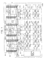
Referring to the block diagram schematically illustrating an active-matrix-type
LCD device according to an embodiment of the present invention shown in
Fig. 1, an LCD panel (display unit) 14 is formed in the following manner. In Fig.
1, m number of row gate lines 11-1 through 11-m formed of, for example,
molybdenum (Mo), and n number of column signal lines 12-1 through 12-n
formed of, for example, aluminum (A1), are arranged in a matrix on a transparent
insulating substrate, for example, a glass substrate (not shown). At the
intersections of the gate lines 11-1 through 11-m and the signal lines 12-1 through
12-n, m ( n unit pixels 13 are formed.
-
Each unit pixel 13 is formed of, as shown in Fig. 2, a TFT (pixel transistor)
15, made of, for example, polysilicon (Poly-Si) generated by laser
recrystallization, a storage capacitor 16, and a liquid crystal capacitor 17. The
TFTs 15 are connected at gate electrodes thereof to the gate lines 11-1 through 11-m
and at source electrodes thereof to the signal lines 12-1 through 12-n.
-
In the unit pixel 13 configured as described above, the liquid crystal
capacitor 17 generates a capacitance between a pixel electrode made of, for
example, indium tin oxide (ITO), connected to the TFT 15, and an opposing
electrode made of, for example, ITO, facing the pixel electrode, via a liquid crystal
material, such as a twisted nematic (TN) liquid crystal. The potential to be
applied to this pixel electrode is written at a high or low level. In this
embodiment, as a common voltage VCOM to be applied to all the opposing
electrodes via Cs lines 29-1 through 29-m, made of, for example, Mo, a
predetermined DC potential is set.
-
In the unit pixel 13, when the TFT 15 is turned on, the optical
transmittance ratio of the liquid crystal is changed, and the storage capacitor 16 is
charged. Accordingly, even if the TFT 15 is turned off, the transmittance ratio of
the liquid crystal is maintained due to the charging voltage of the storage capacitor
16 until the TFT 15 is subsequently switched on. According to this technique. the
quality of a display image on the LCD panel 14 is improved.
-
Referring back to Fig. 1, a vertical drive circuit 18 made of, for example, a
polysilicon TFT, is integrally formed on the same substrate on which the LCD
panel 14 is formed. The vertical dnve circuit 18 selects the unit pixels 13 line-by-line
by sequentially supplying a scanning pulse to the gate lines 11-1 through 11-m,
each line being connected at one end to an output terminal of the vertical drive
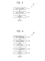
circuit 18, thereby performing vertical scanning. The vertical drive circuit 18 is
formed of, as illustrated in Fig. 3, a shift register 19, a level shifter 20, and a buffer
21.
-
A horizontal drive circuit 22 for supplying signal potentials to the signal
lines 12-l through 12-n in accordance with image data is formed as an external
circuit on a circuit board different from the substrate on which the LCD panel 14
is formed. This will be discussed in greater detail later. Assuming that digital
signals are inputted into the horizontal drive circuit 22, it is necessary to convert
digital signals into analog signals for driving the liquid crystal.
-
To satisfy the above requirement, the horizontal drive circuit 22 is formed
of, as illustrated in Fig. 4, a shift register 23, a level shifter 24, a data latch 25, a
digital-to-analog (D/A) converter 26, and a buffer 27. Digital image data
enabling, for example, at least 8-level 256-color display, is inputted into the
horizontal drive circuit 22.
-
To implement, for example, three-time-division driving corresponding to
red (R), green (G), and blue (B), the n number of column signal lines 12-1 through
12-n are divided by using the number of time-divided portions (in this
embodiment, three) as a unit (block). In this case, as shown in Fig. 1, the
honzontal drive circuit 22 has k number of tape automated bonding (TAB) driver
ICs 28-1 through 28-k (hereinafter referred to as the "TAB IC(1) 28-1 through
TAB IC(k) 28-k") corresponding to the number of units k of the signal lines 12-1
through 12-n.
-
The TAB IC(1) 28-1 through TAB IC(k) 28-k are mounted on an external
circuit board (not shown) different from the substrate on which the LCD panel 14
is formed. The TAB IC(1) 28-1 through TAB IC(k) 28-k sequentially output
signal potentials to the plurality of signal lines of the individual units in time
senes. In this case, to implement the above-described 1H inversion driving, the
signal potentials are outputted by inverting the polarity of the image data in every
1H period for the common voltage VCOM. In response to the above driving
method, k number of time-division switches 30-1 through 30-k are provided for
the input stages of the signal lines 12-1 through 12-n.
-
To effect the three-time-division driving, the time-division switch 30-1 is
formed of, as shown in Fig. 2, three CMOS analog switches (transmission
switches) 31, 32, and 33, each being formed by connecting a PchMOS transistor
and an NchMOS transistor in parallel to each other. The time-division switch 30-1
is formed of a TFT made of, for example, polysilicon, and is integrally formed
with the LCD panel 14 on the same substrate. The other time-division switches
30-2 through 30-k are configured similarly to the time-division switch 30-1.
-
In the time-division switch 30-1, the input terminals of the three analog
switches 31, 32, and 33 are connected to each other, and the common node is
connected to the output terminal of the TAB IC(1) 28-1 via a common signal line
34-1. With this arrangement, the signal potential having an amplitude of, for
example, 0 to 5 V, outputted from the TAB IC(1) 28-1 in time series, is supplied
to the input terminals of the three analog switches 31, 32, and 33 via the common
signal line 34-1. Each of the output terminals of the analog switches 31, 32, and
33 is connected to one end of each of the three signal lines 12-1, 12-2, and 12-3,
respectively.
-
A time-series signal potential is supplied from the TAB IC(2) 28-2 to the
time-division switch 30-2 via a common signal line 34-2. Similarly, a time-senes
signal potential is supplied from the TAB IC(k) 28-k to the time-division switch
30-k via a common signal line 34-k. In this embodiment, for simple
representation, only one common signal line is provided for each TAB IC. In
practice, however, a plurality of common signal lines are provided for a plurality
of output pins of each TAB IC.
-
On the same substrate on which the LCD panel 14 is formed, two control
lines are provided for each analog switch, i.e., a total of six control lines 35-1
through 35-6 are arranged in the direction in which the gate lines 11-1 through 11-m
are arranged. With this arrangement, in the time-division switch 30-1, for
example, two control input terminals (that is, the gate of the NchMOS transistor
and the gate of the PchMOS transistor) of the analog switch 31 are connected to
the control lines 35-1 and 35-2, respectively, two control input terminals of the
analog switch 32 are connected to the control lines 35-3 and 35-4, respectively,
and two control input terminals of the analog switch 33 are connected to the
control lines 35-5 and 35-6, respectively.
-
A description has been given only for the connecting state of the three
analog switches 31 through 33 of the time-division switch 30-1 to the six control
lines 35-1 through 35-6. However, the same applies to the other time-division
switches 30-2 through 30-k.
-
Select pulses S1 through S3 and XS1 through XS3 for respectively
selecting the three analog switches 31 through 33 of each of the time-division
switches 30-1 through 30-k are supplied to the six control lines 35-1 through 35-6
from a select pulse generating circuit 36. The select pulse generating circuit 36 is
separately formed on an external circuit board different from the substrate on
which the LCD panel 14 is formed. The select pulses XS1 through XS3 are
obtained by inverting the select pulses S1 through S3, respectively. In
synchronization with the time-series signal potentials outputted from the TAB
IC(1) 28-1 through TAB IC(k) 28-k, the select pulses S1 through S3 and XS1
through XS3 sequentially activate the analog switches 31 through 33 of each of
the time-division switches 30-1 through 30-k.
-
The select pulses S1 through S3 and XS1 through XS3 are inputted into
the LCD panel 14 from the vicinity of the horizontal drive circuit 22, i.e., via a
plurality of portions from the upper side of the LCD panel 14. More specifically,
six control lines 37-1 through 37-k are respectively laid from the select pulse
generating circuit 36 to the six control lines 35-1 through 35-6 located on the LCD
panel 14 in correspondence with each of the time-division switches 30-1 through
30-k via an external circuit board (not shown) on which the TAB IC(1) 28-1
through TAB IC(k) 28-k are mounted.
-
The wiring of the control lines 35-1 through 35-6 is performed by using,
for example, TAB low-expansion tape. The control lines 35-1 through 35-6
transmit the select pulses S1, XS1, S2, XS2, S3, and XS3, respectively.
-
The above-described configuration in which the select pulses S1 through
S3 and XS1 through XS3 are inputted into the LCD panel 14 is an example only,
and is not intended to limit the invention.
-
The low-level signal potential outputted from the TAB IC(1) 28-1 through
TAB IC(k) 28-k is set to be 0 V (ground potential). In contrast, as the select
pulses S1 through S3 and XS1 through XS3, the low-level potential outputted
from the select pulse generating circuit 36 is set to be lower than the ground
potential, while the high-level potential from the select pulse generating circuit 36
is set to be higher than that (in this embodiment, 5 V) of the signal potential. That
is, the select pulse generating circuit 36 generates the pulses having an amplitude
of, for example, -2 to 9 V.
-
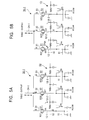
The reason for setting the low-level potential of the select pulses S1
through S3 and XS1 through XS3 to be lower than the ground potential is given
below with reference to Figs. 5A and 5B by taking the operation of the time-division
switch 30-1 by way of example.
-
When the select pulse S1 becomes high and the select pulse XS1 becomes
low so as to activate (conduct) the analog switch 31, as shown in Fig. 5A, a signal
potential supplied from the common signal line 34-1 is written into the signal line
12-1, which is located at the leftmost position among the signal lines 12-1 through
12-3 corresponding to the three-time-division driving. Subsequently, when the
select pulse S2 becomes high and the select pulse XS2 becomes low so as to turn
on the analog switch 32, as illustrated in Fig. 5B, a signal potential is written into
the signal line 12-2, which is located at the middle position.
-
In this case, the signal line 12-1 is not selected and is almost in the floating
state. Then, the signal potential of the signal line 12-2 is transferred to the gate
line 11 and the Cs line 29, both of which are horizontally arranged, and is further
transferred to the non-selected signal line 12-1 via the gate line 11 and the Cs line
29.
-
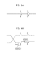
In the 1H inversion driving, the crosstalk caused by the transfer of the
signal potential acts upon an increase in the amplitude potential of the Cs line 29
and the non-selected signal line 12-1. The swing of the Cs line 29 and the
potential of the non-selected signal line 12-1 caused by the crosstalk are indicated
by the waveform diagrams of Figs. 6A and 6B, respectively. The waveform
diagrams reveal that the crosstalk potential (Vspike transferred onto the Cs line 29
changes the potential of the non-selected signal line 12-1 to be lower than the
ground potential (0 V) by about 1.78 V. This is based on simulation results.
-
This causes the signal line 12-1 of the analog switch 31 to be negative. If
the low-level potential of the select pulse S1 is set to be the ground potential, the
gate-source voltage Vgs of the NchTFT exceeds the threshold voltage Vth, thereby
activating the NchTFT.
-
Accordingly, the signal charge stored in the signal line 12-1 flows out to
the common signal line 34-1 via the activated NchTFT, thereby lowering the
signal potential of the signal line 12-1 from the originally written signal potential.
This reduces the pixel potential, resulting in degradation of the image quality in a
TN liquid crystal used in this embodiment.
-
On the other hand, in this embodiment, the low-level potential of the select
pulses S1 through S3 and XS1 through XS3 is set to be, for example, -2 V, as
shown in Fig. 7. Accordingly, even if the potential of the non-selected signal line
12-1, i.e., the source potential of the NchTFT, fluctuates, as shown in Fig. 8, to the
negative side and becomes lower than the ground potential by about 1.78 V owing
to the crosstalk potential (ΔVspike transferred onto the Cs line 29, it does not
become lower than the gate potential of the NchTFT, i.e., it is not less than -2 V.
-
Consequently, the gate-source voltage Vgs of the NchTFT does not exceed
the threshold value Vth while being maintained in the negative state, which would
otherwise activate the NchTFT and cause the signal charge to flow out of the
signal line 12-1 to the common signal line 34-1 via the NchTFT. As a result, the
potential of the non-selected signal line 12-1 is maintained at the originally written
signal potential.
-
In this manner, the low-level potential of the select pulses S1 through S3
and XS1 through XS3 is set lower than the ground potential. Fig. 9 illustrates the
relationship between the leakage voltage (leakage of the signal potential) and the
threshold voltage Vth of the NchTFT. Fig. 9 shows that the threshold voltage Vth
can be used in a higher voltage range compared to the range of the threshold
voltage Vth used when the low-level potential is set to be the ground potential.
Even if the threshold voltage Vth of the NchTFT is reduced due to the process, the
leakage voltage can be sufficiently suppressed. As a result, the high image quality
can be maintained without being influenced by variations in the characteristics of
the transistor. As discussed above, if the low-level potential of the select pulses
S1 through S3 and XS1 through XS3 is set to be, for example, -2 V, the leakage
potential of the signal potential is less than 50 mV, as shown in Fig. 9. Such a
small level of leakage potential can be ignored with almost no degradation in the
image quality.
-
In this embodiment, the low-level potential of the select pulses S1 through
S3 and XS1 through XS3 is set to be lower than the ground potential, assuming
that the low-level potential of the signal potential supplied from the TAB IC(1)
28-1 through TAB IC(k) 28-k is 0 V (ground potential). If it is possible to
increase the low-level potential of the signal potential to the positive side, for
example, to 2 V, the low-level potential of the select pulses S1 through S3 and
XS1 through XS3 can be set to be the ground potential.
-
Similarly, in this embodiment, the high-level potential of the select pulses
S1 through S3 and XS1 through XS3 is set to be, for example, 9 V, assuming that
the high-level potential of the signal potential is 5 V. In short, as long as the high-level
potential of the select pulses S1 through S3 and XS1 through XS3 is set to be
higher than the high-level potential of the signal potential, the leakage potential of
the PchTFTs of the analog switches 31, 32, and 33 can be suppressed.
-
In this embodiment, the 1H inversion drive method is employed in which
the polarity of the image data to be supplied to each pixel is inverted in every 1H
period for the common voltage VCOM. The above-described technique can also
be applied apply to the 1H common (VCOM) inversion drive method in which the
common voltage VCOM is AC-inverted in every 1H period. In the case of the 1H
common inversion drive method, the potential of the Cs line shown in Fig. 10A
and the signal potential of a non-selected signal line shown in Fig. 10B are
inverted in every 1H period.
-
A description is now given, with reference to the timing chart of Fig. 11, of
the operation of the time-division switches 30-1, 30-2, and 30-3 of the active-matrix-type
LCD device constructed in accordance with this embodiment. In Fig.
1, the time-division switch 30-3 and the corresponding TAB IC(3) 28-3 are not
shown.
-
Since the three-time-division driving corresponding to R, G, and B is
employed in this embodiment, the signal potentials for the three pixels, i.e., R, G,
and B, are sequentially outputted in time series from the TAB IC(1) 28-1 through
the TAB IC(3) 28-3 and are transmitted to the time-division switches 30-1, 30-2,
and 30-3 via the common signal lines 34-1, 34-2, and 34-3, respectively.
-
More specifically, the timing chart of Fig. 11 reveals that the signal
potentials of the individual pixels R1, G1, and B1 are transmitted from the TAB
IC(1) 28-1 to the time-division switch 30-1, the signal potentials of the individual
pixels R2, G2, and B2 are transmitted from the TAB IC(2) 28-2 to the time-division
switch 30-2, and the signal potentials of the individual pixels R3, G3, and
B3 are transmitted from the TAB IC(3) 28-3 to the time-division switch 30-3.
The select pulses through S3 and XS1 through XS3 in synchronization with the
above-described time-series signal potentials are also supplied to the time-division
switches 30-1 through 30-3
-
With this arrangement, when the select pulse S1 is at a high level, the
analog switch 31 is turned on, thereby supplying the signal potentials of the pixels
R1 and R3 to the corresponding signal lines among the signal lines 12-1 through
12-n. When the select pulse S2 is at a high level, the analog switch 32 is
activated, thereby supplying the signal potential of the pixel G2 to the
corresponding signal line among the signal lines 12-1 through 12-n. When the
select pulse S3 is at a high level, the analog switch 33 is turned on, thereby
supplying the signal potentials of the pixels B1 and B3 to the corresponding signal
lines among the signal lines 12-1 through 12-n.
-
In this embodiment, the horizontal drive circuit 22 for driving the signal
lines 12-1 through 12-n is placed at one side (upper side in this embodiment) of
the LCD panel 14. However, the honzontal drive circuit 22 may be divided into
two portions with respect to the common voltage VCOM, and the divided portions
may be placed at the upper and lower sides of the LCD panel 14.
-
As is seen from the foregoing description, the present invention offers the
following advantages. In the active-matrix-type LCD device which supplies
signal potentials to signal lines of an LCD panel according to the time-division
drive method, the low-level potential of the select pulses for activating the time-division
switches is set to be lower than the low-level potential of the signal
potential outputted from the horizontal drive circuit. Accordingly, even with the
occurrence of the crosstalk of a signal potential from a selected signal line to a
non-selected signal line, the charge can be prevented from flowing out of the non-selected
signal line via the time-division switch. Thus, the potential of the non-selected
signal line can be maintained at the initially written signal potential. It is
thus possible to eliminate the generation of insufficient contrast and non-uniformity
of the luminance in the honzontal direction caused by the crosstalk of a
signal potential from a selected signal line to a non-selected signal line, thereby
maintaining a high image quality.