EP0990931A2 - Arrangement for adjusting optical components - Google Patents
Arrangement for adjusting optical components Download PDFInfo
- Publication number
- EP0990931A2 EP0990931A2 EP99118932A EP99118932A EP0990931A2 EP 0990931 A2 EP0990931 A2 EP 0990931A2 EP 99118932 A EP99118932 A EP 99118932A EP 99118932 A EP99118932 A EP 99118932A EP 0990931 A2 EP0990931 A2 EP 0990931A2
- Authority
- EP
- European Patent Office
- Prior art keywords
- adjustment
- holding device
- waveguide
- base plate
- marks
- Prior art date
- Legal status (The legal status is an assumption and is not a legal conclusion. Google has not performed a legal analysis and makes no representation as to the accuracy of the status listed.)
- Granted
Links
Images

Classifications
-
- G—PHYSICS
- G02—OPTICS
- G02B—OPTICAL ELEMENTS, SYSTEMS OR APPARATUS
- G02B6/00—Light guides; Structural details of arrangements comprising light guides and other optical elements, e.g. couplings
- G02B6/24—Coupling light guides
- G02B6/42—Coupling light guides with opto-electronic elements
- G02B6/4201—Packages, e.g. shape, construction, internal or external details
- G02B6/4219—Mechanical fixtures for holding or positioning the elements relative to each other in the couplings; Alignment methods for the elements, e.g. measuring or observing methods especially used therefor
- G02B6/4228—Passive alignment, i.e. without a detection of the degree of coupling or the position of the elements
- G02B6/423—Passive alignment, i.e. without a detection of the degree of coupling or the position of the elements using guiding surfaces for the alignment
-
- G—PHYSICS
- G02—OPTICS
- G02B—OPTICAL ELEMENTS, SYSTEMS OR APPARATUS
- G02B6/00—Light guides; Structural details of arrangements comprising light guides and other optical elements, e.g. couplings
- G02B6/24—Coupling light guides
- G02B6/42—Coupling light guides with opto-electronic elements
- G02B6/4201—Packages, e.g. shape, construction, internal or external details
- G02B6/4219—Mechanical fixtures for holding or positioning the elements relative to each other in the couplings; Alignment methods for the elements, e.g. measuring or observing methods especially used therefor
- G02B6/422—Active alignment, i.e. moving the elements in response to the detected degree of coupling or position of the elements
- G02B6/4221—Active alignment, i.e. moving the elements in response to the detected degree of coupling or position of the elements involving a visual detection of the position of the elements, e.g. by using a microscope or a camera
- G02B6/4224—Active alignment, i.e. moving the elements in response to the detected degree of coupling or position of the elements involving a visual detection of the position of the elements, e.g. by using a microscope or a camera using visual alignment markings, e.g. index methods
Definitions
- the invention relates to an arrangement according to the preamble of Claim 1.
- the invention has for its object to provide an arrangement with which a simple adjustment with high accuracy of optical components to each other can be carried out.
- the invention includes an arrangement for coupling in or out light in or out of waveguides.
- the arrangement consists of one on one Base plate applied mirror carrier with mirror surface, at least one Waveguide and a holding device for holding optical or optoelectronic components.
- the mirror support and the holding device have adjustment marks that interlock so that an adjustment first in a direction parallel to the longitudinal extension of the waveguide (x direction) he follows.
- the holding device and the base plate have further adjustment marks, via an adjustment in one, regardless of the previously defined x-direction direction perpendicular to the longitudinal extension of the waveguide (y direction) is guaranteed.
- Optical or optoelectronic components are preferably fitted into a holding opening in the holding device.
- Lenses, light-emitting or laser diodes, photodiodes, glass fiber connectors are used as optical or optoelectronic components.
- Different materials can be used for the base plate, as for all other parts, which preferably consist of semiconductor material or ceramic material or of plastics for printed circuit boards.
- the first adjustment marks are formed in the mirror carrier as a wedge-shaped depression or as a groove and the second adjustment marks are formed in the holding device as wedges or pins protruding from the underside of the holding device and possibly elongated.
- the fourth alignment marks protrude from the underside of the holding device as hemispheres, wedges or conical pins.
- a particular advantage of the invention is that the required positioning accuracy is guaranteed over several process steps. Since the necessary alignment marks for the respective adjustment in the x- or y-direction are on different supports, the respective position in one direction is only determined by snapping two associated alignment marks. For example, the adjustment in the x direction is carried out by a notch on the mirror support, the y direction, which was initially not defined, making no demands on the adjustment accuracy due to the lateral extent of the mirror. The adjustment in the y-direction is independent of this, for example, although a waveguide is precisely arranged in the holding device for the optical component, but it can be displaced along the mirror surface without any loss of quality.
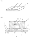
- a mirror support 1 is attached a bevelled mirror surface 11 on the side wall.
- Be the first Adjustment mark 12 is a wedge-shaped groove in the for an adjustment in the x direction Introduced surface.
- 2 is on one Base plate 4 positioned.
- the second alignment mark 21 on the underside of the Holding device 2 engages in the groove of the first alignment mark 12 and uses it to adjust the mirror surface 11 with respect to that introduced in the holding device 2 optical component 5. Lateral displacement along the groove causes only a parallel displacement along the extended mirror surface 11, which is irrelevant for an adjustment in the x direction.
- a lens was chosen that fits into a receiving opening 23 is held precisely.
- the waveguide 3 is up to the mirror surface 11 brought up and can optionally on the contact surface by means of an Refractive index to the medium adapted to the waveguide.
- the Adjustment takes place with the marks 22 and 41 shown in FIG. 3.
- the figure shows a section along the line A of FIG. 2, which is perpendicular to the plane of the drawing runs.
- the third adjustment marks 22 and 12 are used fourth alignment marks 41 so that the waveguide 3 is precise is positioned.
- the waveguide 3 is usually the fourth Adjustment marks 41 made in one process step, making both one accurate have a defined distance from each other. Accordingly, the individual components both the x-direction and the y-direction in their position to each other precisely defined. Wedge-shaped depressions or are used as adjustment marks Grooves in connection with wedges or pins preferably selected as geometries, to cause the components to snap into place when they are joined together.
Abstract
Description
Die Erfindung bezieht sich aufeine Anordnung nach dem Oberbegriff des
Patentanspruchs 1.The invention relates to an arrangement according to the preamble of
In der optischen Verbindungstechnik, der optischen Nachrichtentechnik und in
optischen Systemen ist es erforderlich, einzelne Bauelemente gegeneinander zu
justieren und dabei auch die thermische Ausdehnung von Materialien
unterschiedlicher Wärmeausdehnung zu berücksichtigen. Eine Möglichkeit, eine
präzise Justage durchzuführen ist in Fachkreisen mit dem Begriff ![]()
![]()
Aus der Schrift US 5,748,827 ist eine derartige Anordnung mit zweistufiger Justage bekannt, mit der die Lage mehrerer optischer Bauteile zueinander über eine erste Grobjustage und eine anschließende Feinjustage festgelegt wird. Dabei werden 6 Freiheitsgrade -3 der Translation und 3 der Rotation- erfaßt. Damit die zur Justage vorgesehenen Marken ineinandergreifen, ist bei der Grobjustage beim Zusammenfügen der einzelnen Komponenten eine Positioniergenauigkeit im sub-Millimeterbereich in allen Richtungen erforderlich. Erst mit der Vorrichtung zur Feinjustage wird dann eine Positioniergenauigkeit von einigen Mikrometern erzielt.From the document US 5,748,827 is such an arrangement with two stages Known adjustment with which the position of several optical components relative to one another a first rough adjustment and a subsequent fine adjustment is determined. Here 6 degrees of freedom -3 of translation and 3 of rotation- are recorded. So that Interlocking marks intended for adjustment is in the rough adjustment at Assembling the individual components a positioning accuracy in the sub-millimeter range required in all directions. Only with the device for Fine adjustment then becomes a positioning accuracy of a few micrometers achieved.
Aus der Schrift US 4,268,123 ist eine weitere Anordnung zur Justage beschrieben, mit der optische Komponenten mit geringen Verspannungen gehalten werden können. Durch ein Ineinandergreifen ringförmiger Elemente soll die Spannungsübertragung vom Gehäuse auf die optischen Bauteile vermieden werden.Another arrangement for adjustment is known from the document US Pat. No. 4,268,123 described with the optical components with low tension can be held. By interlocking annular elements the voltage transmission from the housing to the optical components avoided become.
Diese vergleichsweise aufwendigen Techniken sind erforderlich, da alle notwendigen Justagemarken aufeinem Träger aufgebracht sind, und die anderen Komponenten mit großer Genauigkeit an die dafür vorgesehene Stelle positioniert oder über mehrstufige Verfahren grob- und feinjustiert werden müssen. These comparatively complex techniques are necessary because all necessary alignment marks are applied to a carrier, and the other Components with great accuracy in the intended place positioned or roughly and finely adjusted using multi-stage processes have to.
Der Erfindung liegt die Aufgabe zugrunde, eine Anordnung anzugeben, mit der eine einfache Justage mit hoher Genauigkeit optischer Komponenten zueinander durchgeführt werden kann.The invention has for its object to provide an arrangement with which a simple adjustment with high accuracy of optical components to each other can be carried out.
Die Erfindung wird in Bezug aufdie Anordnung durch die Merkmale des
Patentanspruchs 1 wiedergegeben. Die weiteren Ansprüche enthalten vorteilhafte
Aus- und Weiterbildungen der Erfindung.The invention in relation to the arrangement is characterized by the features of
Die Erfindung beinhaltet eine Anordnung zum Ein- oder Auskoppeln von Licht in oder aus Wellenleitern. Die Anordnung besteht aus einem auf einer Grundplatte aufgebrachten Spiegelträger mit Spiegelfläche, mindestens einem Wellenleiter sowie einer Haltevorrichtung zur Aufnahme optischer oder optoelektronischer Bauelemente. Der Spiegelträger und die Haltevorrichtung weisen Justagemarken auf, die so ineinandergreifen, daß eine Justage zunächst in einer zur Längserstreckung des Wellenleiters parallelen Richtung (x-Richtung) erfolgt. Die Haltevorrichtung und die Grundplatte besitzt weitere Justagemarken, über die, unabhängig von der zuvor festgelegten x-Richtung, eine Justage in einer zur Längserstreckung des Wellenleiters senkrechten Richtung (y-Richtung) gewährleistet ist.The invention includes an arrangement for coupling in or out light in or out of waveguides. The arrangement consists of one on one Base plate applied mirror carrier with mirror surface, at least one Waveguide and a holding device for holding optical or optoelectronic components. The mirror support and the holding device have adjustment marks that interlock so that an adjustment first in a direction parallel to the longitudinal extension of the waveguide (x direction) he follows. The holding device and the base plate have further adjustment marks, via an adjustment in one, regardless of the previously defined x-direction direction perpendicular to the longitudinal extension of the waveguide (y direction) is guaranteed.
Dabei sind optische oder optoelektronische Bauelemente bevorzugt in die
Haltevorrichtung in eine Aufnahmeöffnung eingepaßt. Als optische oder
optoelektronische Bauelemente werden Linsen, Leucht- oder Laserdioden,
Photodioden, Glasfaserstecker verwendet.
Für die Grundplatte, wie auch für alle anderen Teile, können unterschiedliche
Materialien Verwendung finden, die bevorzugt aus Halbleitermaterial oder
keramischem Material oder aus Kunststoffen für Leiterplatten bestehen. Optical or optoelectronic components are preferably fitted into a holding opening in the holding device. Lenses, light-emitting or laser diodes, photodiodes, glass fiber connectors are used as optical or optoelectronic components.
Different materials can be used for the base plate, as for all other parts, which preferably consist of semiconductor material or ceramic material or of plastics for printed circuit boards.
Die ersten Justagemarken sind im Spiegelträger als keilförmige Einsenkung oder
als Nut und die zweiten Justagemarken sind in der Haltevorrichtung als aus der
Unterseite der Haltevorrichtung herausragende und gegebenenfalls langgestreckte
Keile oder Zapfen ausgebildet.
Die vierten Justagemarken ragen aus der Unterseite der Haltevorrichtung als
Halbkugeln, Keile oder konische Zapfen heraus.The first adjustment marks are formed in the mirror carrier as a wedge-shaped depression or as a groove and the second adjustment marks are formed in the holding device as wedges or pins protruding from the underside of the holding device and possibly elongated.
The fourth alignment marks protrude from the underside of the holding device as hemispheres, wedges or conical pins.
Ein besonderer Vorteil der Erfindung besteht darin, daß die erforderliche
Positioniergenauigkeit über mehrere Prozeßschritte hinweg gewährleistet ist. Da
die notwendigen Justagemarken für die jeweilige Justage in x- oder y-Richtung
sich auf unterschiedlichen Trägern befinden, wird lediglich durch ein Einrasten
zweier zusammengehöriger Justagemarken die jeweilige Position in einer
Richtung festgelegt. Beispielsweise erfolgt die Justage in x-Richtung durch eine
Kerbe aufdem Spiegelträger, wobei die zunächst nicht definierte y-Richtung
infolge der lateralen Ausdehnung des Spiegels keine Anforderungen an die
Justiergenauigkeit stellt. Die Justage in y-Richtung erfolgt davon unabhängig,
indem beispielsweise ein Wellenleiter zwar zum optischen Bauteil in der
Haltevorrichtung präzise angeordnet wird, dieserjedoch ohne Qualitätseinbuße
entlang der Spiegelfläche versetzt werden kann.
Insgesamt reicht für die Justage eine Genauigkeit von wenigen mm in beiden
Justageschritten aus, um die Haltevorrichtung für die optischen Bauteile dennoch
aufwenige Mikrometer genau über dem Wellenleiter zu positionieren.
Ein weiterer Vorteil der Anordnung ist darin zu sehen, daß die Justage in x- und
y-Richtung passiv, durch Einrasten bewerkstelligt wird und nicht unter einem
Mikroskop an die richtige Stelle gebracht werden muß. A particular advantage of the invention is that the required positioning accuracy is guaranteed over several process steps. Since the necessary alignment marks for the respective adjustment in the x- or y-direction are on different supports, the respective position in one direction is only determined by snapping two associated alignment marks. For example, the adjustment in the x direction is carried out by a notch on the mirror support, the y direction, which was initially not defined, making no demands on the adjustment accuracy due to the lateral extent of the mirror. The adjustment in the y-direction is independent of this, for example, although a waveguide is precisely arranged in the holding device for the optical component, but it can be displaced along the mirror surface without any loss of quality.
Overall, an accuracy of a few mm is sufficient in both adjustment steps for the adjustment in order to position the holding device for the optical components exactly a few micrometers precisely above the waveguide.
Another advantage of the arrangement can be seen in the fact that the adjustment in the x and y direction is done passively, by snapping in, and does not have to be brought into the correct place under a microscope.
Im folgenden wird die Erfindung anhand von vorteilhaften Ausführungsbeispielen unter Bezugnahme auf schematische Zeichnungen in den Figuren näher erläutert. Es zeigen:
- Fig. 1
- Spiegelträger mit erster Justagemarke,
- Fig. 2
- Schnitt der Anordnung parallel zur Wellenleiterlängsachse (Seitenansicht),
- Fig. 3
- Schnitt der Anordnung senkrecht zur Wellenleiterlängsachse (entlang der in Fig.2 dargestellten Linie A; Vorderansicht).
- Fig. 1
- Mirror carrier with first adjustment mark,
- Fig. 2
- Section of the arrangement parallel to the longitudinal axis of the waveguide (side view),
- Fig. 3
- Section of the arrangement perpendicular to the longitudinal axis of the waveguide (along the line A shown in FIG. 2; front view).
In einem ersten Ausführungsbeispiel gemäß Fig. 1 wird ein Spiegelträger 1 mit
einer an der Seitenwand abgeschrägten Spiegelfläche 11 dargestellt. Als erste
Justagemarke 12 ist für eine Justage in x-Richtung eine keilförmige Nut in die
Oberfläche eingebracht. Der Spiegelträger 1 ist gemäß Fig. 2 aufeiner
Grundplatte 4 positioniert. Die zweite Justagemarke 21 aufder Unterseite der
Haltevorrichtung 2 greift in die Nut der ersten Justagemarke 12 und justiert damit
die Spiegelfläche 11 bezüglich des in der Haltevorrichtung 2 eingebrachten
optischen Bauelements 5. Eine laterale Verschiebung entlang der Nut bewirkt
lediglich eine parallele Verschiebung entlang der ausgedehnten Spiegelfläche 11,
die für eine Justage in x-Richtung unmaßgeblich ist. Als optisches Bauelement 5
wurde in diesem Fall eine Linse gewählt, die in einer Aufnahmeöffnung 23
präzise gehaltert wird. Der Wellenleiter 3 ist bis zur Spiegelfläche 11
herangeführt und kann gegebenenfalls an der Berührungsfläche mittels eines im
Brechungsindex an den Wellenleiter angepaßten Mediums verbunden sein. Die
Justage erfolgt mit den in Fig.3 dargestellten Marken 22 und 41. Die Figur zeigt
einen Schnitt entlang der Linie A der Fig. 2, der senkrecht zur Zeichenebene
verläuft. Zur Justage in y-Richtung greifen die dritten Justagemarken 22 und die
vierten Justagemarken 41 so ineinander, daß der Wellenleiter 3 präzise
positioniert wird. Der Wellenleiter 3 wird üblicherweise mit den vierten
Justagemarken 41 in einem Prozeßschritt hergestellt, wodurch beide einen genau
definierten Abstand zueinander besitzen. Demnach sind die einzelnen Bauteile
sowohl die x-Richtung wie auch die y-Richtung in ihrer Position zueinander
genau festgelegt. Als Justagemarken werden keilförmige Einsenkungen oder
Nuten in Verbindung mit Keilen oder Zapfen bevorzugt als Geometrien gewählt,
um einen Einrastvorgang der Bauteile beim Zusammenfügen zu bewirken.In a first exemplary embodiment according to FIG. 1, a
Claims (6)
dadurch gekennzeichnet,
characterized,
Applications Claiming Priority (2)
| Application Number | Priority Date | Filing Date | Title |
|---|---|---|---|
| DE19845227 | 1998-10-01 | ||
| DE19845227A DE19845227A1 (en) | 1998-10-01 | 1998-10-01 | Arrangement for adjusting optical components |
Publications (3)
| Publication Number | Publication Date |
|---|---|
| EP0990931A2 true EP0990931A2 (en) | 2000-04-05 |
| EP0990931A3 EP0990931A3 (en) | 2002-06-05 |
| EP0990931B1 EP0990931B1 (en) | 2006-06-14 |
Family
ID=7883057
Family Applications (1)
| Application Number | Title | Priority Date | Filing Date |
|---|---|---|---|
| EP99118932A Expired - Lifetime EP0990931B1 (en) | 1998-10-01 | 1999-09-25 | Device for coupling light into and out of waveguides and method of its production |
Country Status (6)
| Country | Link |
|---|---|
| US (1) | US6236788B1 (en) |
| EP (1) | EP0990931B1 (en) |
| AT (1) | ATE330241T1 (en) |
| CA (1) | CA2284420C (en) |
| DE (2) | DE19845227A1 (en) |
| ES (1) | ES2267217T3 (en) |
Families Citing this family (23)
| Publication number | Priority date | Publication date | Assignee | Title |
|---|---|---|---|---|
| US6775440B2 (en) * | 2000-04-28 | 2004-08-10 | Kyocera Corporation | Optical module and carrier for optical module |
| SE519713C2 (en) * | 2000-05-23 | 2003-04-01 | Ericsson Telefon Ab L M | Passive alignment method and device |
| US6737223B2 (en) * | 2000-08-07 | 2004-05-18 | Shipley Company, L.L.C. | Fiber optic chip with lenslet array and method of fabrication |
| US7086134B2 (en) * | 2000-08-07 | 2006-08-08 | Shipley Company, L.L.C. | Alignment apparatus and method for aligning stacked devices |
| US6724961B2 (en) * | 2002-02-14 | 2004-04-20 | Corona Optical Systems, Inc. | Method to assemble optical components to a substrate |
| EP1485116A4 (en) * | 2002-02-27 | 2006-06-07 | Univ Wake Forest | Angiotensin-(1-7) and angiotensin-(1-7) agonists for inhibition of cancer cell growth |
| JP3974459B2 (en) * | 2002-06-11 | 2007-09-12 | 沖電気工業株式会社 | Optical element, mounting method thereof, and optical module |
| NL1021205C2 (en) * | 2002-08-02 | 2004-02-18 | Framatome Connectors Int | Optical connector assembly, coupling piece and method for positioning the coupling piece and a structure of waveguides. |
| SE525405C2 (en) * | 2002-08-09 | 2005-02-15 | Acreo Ab | Mirrors for polymeric guides, process for their preparation, and optical waveguide device |
| US7137745B2 (en) * | 2003-03-19 | 2006-11-21 | Oki Electric Industry Co., Ltd. | Subassembly and optical module |
| KR100528972B1 (en) * | 2003-10-27 | 2005-11-16 | 한국전자통신연구원 | Optical printed circuit board system with taper shaped-waveguides |
| US7212698B2 (en) * | 2004-02-10 | 2007-05-01 | International Business Machines Corporation | Circuit board integrated optical coupling elements |
| DE102004029694B3 (en) * | 2004-06-14 | 2005-10-20 | Siemens Ag | Manufacturing process for optoelectronic building block involves first gripper lowering deflector block into cutout with UV-hardening adhesive and second gripper positioning transmitter/receiver block |
| US7308167B2 (en) * | 2004-09-01 | 2007-12-11 | Agilent Technologies, Inc. | Optical assembly with optoelectronic device alignment |
| JP2006301610A (en) * | 2005-03-25 | 2006-11-02 | Fuji Xerox Co Ltd | Optical coupling device |
| WO2007076888A1 (en) * | 2005-12-30 | 2007-07-12 | Fci | Optical coupling device |
| US7421160B1 (en) * | 2007-04-10 | 2008-09-02 | International Business Machines Corporation | Coupling element alignment using waveguide fiducials |
| TWI368768B (en) * | 2007-12-28 | 2012-07-21 | Ind Tech Res Inst | Optical intermediary component and optical daughter card module |
| EP2378993B1 (en) * | 2008-12-23 | 2017-03-08 | Mako Surgical Corp. | Transmission with adjustment member for varying tension force |
| CN103270443B (en) * | 2010-12-21 | 2015-07-08 | 日本电气株式会社 | Optical module and method of manufacturing same |
| AT512168B1 (en) | 2012-01-30 | 2013-06-15 | Sola Messwerkzeuge Gmbh | MARKING PROJECTOR |
| CN106461890A (en) * | 2014-05-15 | 2017-02-22 | 纳米精密产品股份有限公司 | Demountable optical connector for optoelectronic devices |
| US11500166B2 (en) | 2020-02-03 | 2022-11-15 | Senko Advanced Components, Inc. | Elastic averaging coupling |
Citations (7)
| Publication number | Priority date | Publication date | Assignee | Title |
|---|---|---|---|---|
| JPS61133911A (en) * | 1984-12-03 | 1986-06-21 | Nippon Telegr & Teleph Corp <Ntt> | Coupling method of light emitting element and photodetector as well as optical waveguide |
| EP0463457A2 (en) * | 1990-06-22 | 1992-01-02 | International Business Machines Corporation | Methods and apparatus for precise alignment of objects |
| US5345524A (en) * | 1993-05-20 | 1994-09-06 | Motorola, Inc. | Optoelectronic transceiver sub-module and method for making |
| WO1996007117A1 (en) * | 1994-08-29 | 1996-03-07 | Akzo Nobel N.V. | Connector for polymeric optical waveguide structures |
| US5748827A (en) * | 1996-10-23 | 1998-05-05 | University Of Washington | Two-stage kinematic mount |
| WO1998035253A1 (en) * | 1997-02-07 | 1998-08-13 | Bookham Technology Limited | Device for re-directing light from optical waveguide |
| WO1999050700A1 (en) * | 1998-03-31 | 1999-10-07 | Honeywell Inc. | Chip-to-interface alignment |
Family Cites Families (7)
| Publication number | Priority date | Publication date | Assignee | Title |
|---|---|---|---|---|
| US4268123A (en) * | 1979-02-26 | 1981-05-19 | Hughes Aircraft Company | Kinematic mount |
| DE4313493A1 (en) * | 1992-11-25 | 1994-05-26 | Ant Nachrichtentech | Arrangement for coupling an optical waveguide to a light-emitting or receiving element |
| TW255015B (en) * | 1993-11-05 | 1995-08-21 | Motorola Inc | |
| US5416870A (en) * | 1993-12-03 | 1995-05-16 | Motorola, Inc. | Optoelectronic interface device and method with reflective surface |
| DE4416563C1 (en) * | 1994-05-11 | 1995-07-20 | Ant Nachrichtentech | Coupler for connecting opto-electronic device to waveguide |
| US5479540A (en) * | 1994-06-30 | 1995-12-26 | The Whitaker Corporation | Passively aligned bi-directional optoelectronic transceiver module assembly |
| US6115521A (en) * | 1998-05-07 | 2000-09-05 | Trw Inc. | Fiber/waveguide-mirror-lens alignment device |
-
1998
- 1998-10-01 DE DE19845227A patent/DE19845227A1/en not_active Ceased
-
1999
- 1999-09-25 DE DE59913550T patent/DE59913550D1/en not_active Expired - Lifetime
- 1999-09-25 ES ES99118932T patent/ES2267217T3/en not_active Expired - Lifetime
- 1999-09-25 EP EP99118932A patent/EP0990931B1/en not_active Expired - Lifetime
- 1999-09-25 AT AT99118932T patent/ATE330241T1/en not_active IP Right Cessation
- 1999-09-30 CA CA002284420A patent/CA2284420C/en not_active Expired - Fee Related
- 1999-10-01 US US09/409,879 patent/US6236788B1/en not_active Expired - Lifetime
Patent Citations (7)
| Publication number | Priority date | Publication date | Assignee | Title |
|---|---|---|---|---|
| JPS61133911A (en) * | 1984-12-03 | 1986-06-21 | Nippon Telegr & Teleph Corp <Ntt> | Coupling method of light emitting element and photodetector as well as optical waveguide |
| EP0463457A2 (en) * | 1990-06-22 | 1992-01-02 | International Business Machines Corporation | Methods and apparatus for precise alignment of objects |
| US5345524A (en) * | 1993-05-20 | 1994-09-06 | Motorola, Inc. | Optoelectronic transceiver sub-module and method for making |
| WO1996007117A1 (en) * | 1994-08-29 | 1996-03-07 | Akzo Nobel N.V. | Connector for polymeric optical waveguide structures |
| US5748827A (en) * | 1996-10-23 | 1998-05-05 | University Of Washington | Two-stage kinematic mount |
| WO1998035253A1 (en) * | 1997-02-07 | 1998-08-13 | Bookham Technology Limited | Device for re-directing light from optical waveguide |
| WO1999050700A1 (en) * | 1998-03-31 | 1999-10-07 | Honeywell Inc. | Chip-to-interface alignment |
Non-Patent Citations (3)
| Title |
|---|
| LASER FOCUS WORLD, BUYERS GUIDE, Bd. 32, Nr. 13, 15. Dezember 1996 (1996-12-15), Seite 682 XP002195019 * |
| LINDEN VAN DER J E ET AL: "MICROMACHINED PHOTODIODE SUBMOUNT WITH INTEGRATED MIRROR FOR EFFICIENT OUT-OF-PLANE COUPLING TO PLANAR POLYMERIC WAVEGUIDE CIRCUITS" JAPANESE JOURNAL OF APPLIED PHYSICS, PUBLICATION OFFICE JAPANESE JOURNAL OF APPLIED PHYSICS. TOKYO, JP, Bd. 37, Nr. 6B, Juni 1998 (1998-06), Seiten 3730-3735, XP000860818 ISSN: 0021-4922 * |
| PATENT ABSTRACTS OF JAPAN vol. 010, no. 327 (P-513), 7. November 1986 (1986-11-07) & JP 61 133911 A (NIPPON TELEGR & TELEPH CORP), 21. Juni 1986 (1986-06-21) * |
Also Published As
| Publication number | Publication date |
|---|---|
| DE19845227A1 (en) | 2000-04-06 |
| ATE330241T1 (en) | 2006-07-15 |
| US6236788B1 (en) | 2001-05-22 |
| CA2284420C (en) | 2009-07-21 |
| DE59913550D1 (en) | 2006-07-27 |
| CA2284420A1 (en) | 2000-04-01 |
| ES2267217T3 (en) | 2007-03-01 |
| EP0990931A3 (en) | 2002-06-05 |
| EP0990931B1 (en) | 2006-06-14 |
Similar Documents
| Publication | Publication Date | Title |
|---|---|---|
| EP0990931B1 (en) | Device for coupling light into and out of waveguides and method of its production | |
| DE19819164C1 (en) | Optical data communication module | |
| DE10238741A1 (en) | Planar optical component and coupling device for coupling light between a planar optical component and an optical component | |
| WO2006047896A1 (en) | Fibre-lens arrangement and lens array for one such fibre-lens arrangement | |
| EP3665491A1 (en) | Position-tolerance-insensitive contacting module for contacting optoelectronic chips | |
| EP0194613A2 (en) | Method for the precise assembly of parts of an optical device | |
| DE19644758A1 (en) | Centering arrangement for positioning micro-structured bodies | |
| DE69724331T2 (en) | Method for producing a nozzle body and working device | |
| DE19844701C1 (en) | Method for adjusting an optoelectronic component and component | |
| EP0779526A2 (en) | Optical and/or electrooptical connection and process for its fabrication | |
| DE102010047805A1 (en) | Laser processing device | |
| DE4240950C1 (en) | Method for producing a cover for an integrated optical circuit and cover for an integrated optical circuit | |
| DE3929944C2 (en) | ||
| DE19805040A1 (en) | Optical co-ordinate measuring machine using light transmission | |
| DE19704502C1 (en) | Laser module with fine adjustment method e.g. for micrometre range transmission engineering | |
| EP0783715B1 (en) | Optical coupling arrangement | |
| DE4109196A1 (en) | DEVICE FOR COUPLING LIGHTWAVE GUIDES | |
| DE4101043C2 (en) | ||
| DE4002370B4 (en) | Method and device for adjusting the optical coupling of optical waveguides and optical components | |
| EP0918237A1 (en) | Optical device | |
| DE102007024961A1 (en) | Device for changing the distance between light beam axes and substrate exposure device | |
| DE4133220C2 (en) | Fiber-lens arrangement for optical coupling | |
| DE102019009399B4 (en) | Optical device | |
| DE4342844C1 (en) | Electro-optical module | |
| DE3246358A1 (en) | Device for the antibacklash displacement of objects in a coordinate system |
Legal Events
| Date | Code | Title | Description |
|---|---|---|---|
| PUAI | Public reference made under article 153(3) epc to a published international application that has entered the european phase |
Free format text: ORIGINAL CODE: 0009012 |
|
| AK | Designated contracting states |
Kind code of ref document: A2 Designated state(s): AT BE CH CY DE DK ES FI FR GB GR IE IT LI LU MC NL PT SE |
|
| AX | Request for extension of the european patent |
Free format text: AL;LT;LV;MK;RO;SI |
|
| PUAL | Search report despatched |
Free format text: ORIGINAL CODE: 0009013 |
|
| AK | Designated contracting states |
Kind code of ref document: A3 Designated state(s): AT BE CH CY DE DK ES FI FR GB GR IE IT LI LU MC NL PT SE |
|
| AX | Request for extension of the european patent |
Free format text: AL;LT;LV;MK;RO;SI |
|
| 17P | Request for examination filed |
Effective date: 20021128 |
|
| AKX | Designation fees paid |
Designated state(s): AT BE CH CY DE DK ES FI FR GB GR IE IT LI LU MC NL PT SE |
|
| 17Q | First examination report despatched |
Effective date: 20030122 |
|
| GRAP | Despatch of communication of intention to grant a patent |
Free format text: ORIGINAL CODE: EPIDOSNIGR1 |
|
| RTI1 | Title (correction) |
Free format text: DEVICE FOR COUPLING LIGHT INTO AND OUT OF WAVEGUIDES AND METHOD OF ITS PRODUCTION |
|
| GRAS | Grant fee paid |
Free format text: ORIGINAL CODE: EPIDOSNIGR3 |
|
| GRAA | (expected) grant |
Free format text: ORIGINAL CODE: 0009210 |
|
| AK | Designated contracting states |
Kind code of ref document: B1 Designated state(s): AT BE CH CY DE DK ES FI FR GB GR IE IT LI LU MC NL PT SE |
|
| PG25 | Lapsed in a contracting state [announced via postgrant information from national office to epo] |
Ref country code: IE Free format text: LAPSE BECAUSE OF FAILURE TO SUBMIT A TRANSLATION OF THE DESCRIPTION OR TO PAY THE FEE WITHIN THE PRESCRIBED TIME-LIMIT Effective date: 20060614 |
|
| REG | Reference to a national code |
Ref country code: GB Ref legal event code: FG4D Free format text: NOT ENGLISH |
|
| REG | Reference to a national code |
Ref country code: CH Ref legal event code: EP |
|
| REG | Reference to a national code |
Ref country code: IE Ref legal event code: FG4D Free format text: LANGUAGE OF EP DOCUMENT: GERMAN |
|
| REF | Corresponds to: |
Ref document number: 59913550 Country of ref document: DE Date of ref document: 20060727 Kind code of ref document: P |
|
| PG25 | Lapsed in a contracting state [announced via postgrant information from national office to epo] |
Ref country code: DK Free format text: LAPSE BECAUSE OF FAILURE TO SUBMIT A TRANSLATION OF THE DESCRIPTION OR TO PAY THE FEE WITHIN THE PRESCRIBED TIME-LIMIT Effective date: 20060914 |
|
| PG25 | Lapsed in a contracting state [announced via postgrant information from national office to epo] |
Ref country code: MC Free format text: LAPSE BECAUSE OF NON-PAYMENT OF DUE FEES Effective date: 20060930 Ref country code: BE Free format text: LAPSE BECAUSE OF NON-PAYMENT OF DUE FEES Effective date: 20060930 |
|
| REG | Reference to a national code |
Ref country code: SE Ref legal event code: TRGR |
|
| RAP2 | Party data changed (patent owner data changed or rights of a patent transferred) |
Owner name: ERNI MANAGEMENT AG |
|
| REG | Reference to a national code |
Ref country code: GB Ref legal event code: 732E |
|
| GBT | Gb: translation of ep patent filed (gb section 77(6)(a)/1977) |
Effective date: 20061018 |
|
| PG25 | Lapsed in a contracting state [announced via postgrant information from national office to epo] |
Ref country code: PT Free format text: LAPSE BECAUSE OF FAILURE TO SUBMIT A TRANSLATION OF THE DESCRIPTION OR TO PAY THE FEE WITHIN THE PRESCRIBED TIME-LIMIT Effective date: 20061114 |
|
| NLT2 | Nl: modifications (of names), taken from the european patent patent bulletin |
Owner name: ERNI MANAGEMENT AG Effective date: 20061018 |
|
| REG | Reference to a national code |
Ref country code: IE Ref legal event code: FD4D |
|
| ET | Fr: translation filed | ||
| REG | Reference to a national code |
Ref country code: CH Ref legal event code: PUE Owner name: ERNI MANAGEMENT AG Free format text: DAIMLERCHRYSLER AG#EPPLESTRASSE 225#70567 STUTTGART (DE) -TRANSFER TO- ERNI MANAGEMENT AG#BAHNHOFSTRASSE 4#6052 HERGISWIL (CH) Ref country code: CH Ref legal event code: NV Representative=s name: ISLER & PEDRAZZINI AG |
|
| REG | Reference to a national code |
Ref country code: ES Ref legal event code: FG2A Ref document number: 2267217 Country of ref document: ES Kind code of ref document: T3 |
|
| PLBE | No opposition filed within time limit |
Free format text: ORIGINAL CODE: 0009261 |
|
| STAA | Information on the status of an ep patent application or granted ep patent |
Free format text: STATUS: NO OPPOSITION FILED WITHIN TIME LIMIT |
|
| 26N | No opposition filed |
Effective date: 20070315 |
|
| REG | Reference to a national code |
Ref country code: CH Ref legal event code: PCAR Free format text: ISLER & PEDRAZZINI AG;POSTFACH 1772;8027 ZUERICH (CH) |
|
| NLS | Nl: assignments of ep-patents |
Owner name: ERNI MANAGEMENT AG Effective date: 20070815 |
|
| PG25 | Lapsed in a contracting state [announced via postgrant information from national office to epo] |
Ref country code: AT Free format text: LAPSE BECAUSE OF NON-PAYMENT OF DUE FEES Effective date: 20060925 |
|
| BERE | Be: lapsed |
Owner name: DAIMLERCHRYSLER A.G. Effective date: 20060930 |
|
| PG25 | Lapsed in a contracting state [announced via postgrant information from national office to epo] |
Ref country code: GR Free format text: LAPSE BECAUSE OF FAILURE TO SUBMIT A TRANSLATION OF THE DESCRIPTION OR TO PAY THE FEE WITHIN THE PRESCRIBED TIME-LIMIT Effective date: 20060915 |
|
| PG25 | Lapsed in a contracting state [announced via postgrant information from national office to epo] |
Ref country code: LU Free format text: LAPSE BECAUSE OF NON-PAYMENT OF DUE FEES Effective date: 20060925 |
|
| PG25 | Lapsed in a contracting state [announced via postgrant information from national office to epo] |
Ref country code: CY Free format text: LAPSE BECAUSE OF FAILURE TO SUBMIT A TRANSLATION OF THE DESCRIPTION OR TO PAY THE FEE WITHIN THE PRESCRIBED TIME-LIMIT Effective date: 20060614 |
|
| PGFP | Annual fee paid to national office [announced via postgrant information from national office to epo] |
Ref country code: ES Payment date: 20090928 Year of fee payment: 11 |
|
| PGFP | Annual fee paid to national office [announced via postgrant information from national office to epo] |
Ref country code: SE Payment date: 20090922 Year of fee payment: 11 Ref country code: FI Payment date: 20090923 Year of fee payment: 11 |
|
| REG | Reference to a national code |
Ref country code: CH Ref legal event code: PUE Owner name: VARIO-OPTICS AG Free format text: ERNI MANAGEMENT AG#BAHNHOFSTRASSE 4#6052 HERGISWIL (CH) -TRANSFER TO- VARIO-OPTICS AG#MITTELBISSAUSTRASSE 7#9410 HEIDEN (CH) Ref country code: CH Ref legal event code: NV Representative=s name: PATENTANWALTSBUERO DR. URS FALK |
|
| REG | Reference to a national code |
Ref country code: FR Ref legal event code: TP |
|
| PGFP | Annual fee paid to national office [announced via postgrant information from national office to epo] |
Ref country code: IT Payment date: 20090923 Year of fee payment: 11 |
|
| REG | Reference to a national code |
Ref country code: GB Ref legal event code: 732E Free format text: REGISTERED BETWEEN 20101021 AND 20101027 |
|
| REG | Reference to a national code |
Ref country code: NL Ref legal event code: SD Effective date: 20101125 |
|
| REG | Reference to a national code |
Ref country code: SE Ref legal event code: EUG |
|
| PG25 | Lapsed in a contracting state [announced via postgrant information from national office to epo] |
Ref country code: FI Free format text: LAPSE BECAUSE OF NON-PAYMENT OF DUE FEES Effective date: 20100925 Ref country code: IT Free format text: LAPSE BECAUSE OF NON-PAYMENT OF DUE FEES Effective date: 20100925 |
|
| REG | Reference to a national code |
Ref country code: ES Ref legal event code: FD2A Effective date: 20111020 |
|
| PG25 | Lapsed in a contracting state [announced via postgrant information from national office to epo] |
Ref country code: ES Free format text: LAPSE BECAUSE OF NON-PAYMENT OF DUE FEES Effective date: 20100926 |
|
| PG25 | Lapsed in a contracting state [announced via postgrant information from national office to epo] |
Ref country code: SE Free format text: LAPSE BECAUSE OF NON-PAYMENT OF DUE FEES Effective date: 20100926 |
|
| REG | Reference to a national code |
Ref country code: FR Ref legal event code: PLFP Year of fee payment: 18 |
|
| REG | Reference to a national code |
Ref country code: FR Ref legal event code: PLFP Year of fee payment: 19 |
|
| REG | Reference to a national code |
Ref country code: FR Ref legal event code: PLFP Year of fee payment: 20 |
|
| PGFP | Annual fee paid to national office [announced via postgrant information from national office to epo] |
Ref country code: FR Payment date: 20180924 Year of fee payment: 20 |
|
| PGFP | Annual fee paid to national office [announced via postgrant information from national office to epo] |
Ref country code: GB Payment date: 20180924 Year of fee payment: 20 Ref country code: CH Payment date: 20180927 Year of fee payment: 20 Ref country code: NL Payment date: 20180924 Year of fee payment: 20 |
|
| PGFP | Annual fee paid to national office [announced via postgrant information from national office to epo] |
Ref country code: DE Payment date: 20181001 Year of fee payment: 20 |
|
| REG | Reference to a national code |
Ref country code: DE Ref legal event code: R071 Ref document number: 59913550 Country of ref document: DE Ref country code: NL Ref legal event code: MK Effective date: 20190924 |
|
| REG | Reference to a national code |
Ref country code: CH Ref legal event code: PL |
|
| REG | Reference to a national code |
Ref country code: GB Ref legal event code: PE20 Expiry date: 20190924 |
|
| PG25 | Lapsed in a contracting state [announced via postgrant information from national office to epo] |
Ref country code: GB Free format text: LAPSE BECAUSE OF EXPIRATION OF PROTECTION Effective date: 20190924 |