EP0992068B1 - Sram-zellenanordnung und verfahren zu deren herstellung - Google Patents
Sram-zellenanordnung und verfahren zu deren herstellung Download PDFInfo
- Publication number
- EP0992068B1 EP0992068B1 EP98934869A EP98934869A EP0992068B1 EP 0992068 B1 EP0992068 B1 EP 0992068B1 EP 98934869 A EP98934869 A EP 98934869A EP 98934869 A EP98934869 A EP 98934869A EP 0992068 B1 EP0992068 B1 EP 0992068B1
- Authority
- EP
- European Patent Office
- Prior art keywords
- transistor
- source
- drain region
- trench
- conductive structure
- Prior art date
- Legal status (The legal status is an assumption and is not a legal conclusion. Google has not performed a legal analysis and makes no representation as to the accuracy of the status listed.)
- Expired - Lifetime
Links
Images


Classifications
-
- H—ELECTRICITY
- H10—SEMICONDUCTOR DEVICES; ELECTRIC SOLID-STATE DEVICES NOT OTHERWISE PROVIDED FOR
- H10B—ELECTRONIC MEMORY DEVICES
- H10B10/00—Static random access memory [SRAM] devices
-
- H—ELECTRICITY
- H10—SEMICONDUCTOR DEVICES; ELECTRIC SOLID-STATE DEVICES NOT OTHERWISE PROVIDED FOR
- H10B—ELECTRONIC MEMORY DEVICES
- H10B10/00—Static random access memory [SRAM] devices
- H10B10/12—Static random access memory [SRAM] devices comprising a MOSFET load element
Definitions
- the invention relates to an SRAM cell arrangement in which one Memory cell comprises six transistors.
- An SRAM cell array is a memory cell array with random access to stored information. In contrast to a DRAM cell arrangement in which the information needs to be refreshed at regular intervals the information is stored statically.
- a 6 T memory cell comprises four MOS transistors connected as flip-flops and two Select transistors.
- the flip-flop is stable in one of two States.
- the state of the flip-flop represents a logical one Size, 0 or 1, by controlling the selection transistors over a word line can over two bit lines both the state determines and thus the information read out as well as the state changed and thus new information get saved.
- a 6T memory cell that can be produced with an area of 55F 2 , where F is the minimum structure size that can be produced in the respective technology.
- Self-aligned contacts that is, those produced without the use of masks to be adjusted, as well as local connections, ie connections that lie within the cell, are used.
- the invention is based on the problem of an SRAM cell arrangement specify the 6 T memory cells as memory cells includes and with particularly high packing density can be produced. Furthermore, a manufacturing process for such an SRAM cell arrangement can be specified.
- a first source / drain region of a first transistor is with a first source / drain region of a second Transistor and a first voltage connection connected.
- On second source / drain region of the first transistor is with a first source / drain region of a third transistor, a first source / drain region of a fifth transistor, a gate electrode of the second transistor and a gate electrode a fourth transistor connected.
- a gate electrode the first transistor is connected to a second Source / drain region of the second transistor, a first Source / drain region of the fourth transistor, a gate electrode of the third transistor and a first source / drain region a sixth transistor connected.
- a second The source / drain region of the third transistor is connected to a second source / drain region of the fourth transistor and one second voltage connection connected.
- a second source / drain region the fifth transistor is connected to a first Bit line connected.
- a gate electrode of the fifth transistor is with a gate electrode of the sixth transistor and connected to a word line.
- a second source / drain region the sixth transistor is connected to a second Bit line connected.
- the third transistor and the fourth Transistors are complementary to the first transistor second transistor, fifth transistor and sixth Transistor. It is within the scope of the invention for improvement various properties of the SRAM cell arrangement in addition to the six transistors in a memory cell Components such as Capacitors to the memory cell too integrate.
- the six transistors are on the edges of strip-shaped, depressions that run parallel to one another and act as trenches can be realized in a substrate, formed, whereby the density of the connections increases and the area of the Memory cell is reduced.
- the first transistor and the second transistor are on a second edge of a first Grabens
- the fifth transistor and the sixth transistor are on a second flank of a second trench
- the third transistor and the fourth transistor are connected to one first flank of a fourth trench.
- Third trenches filled with insulating material can be used as insulating structures parts of mutually complementary Isolate transistors from each other.
- gate electrodes of the six transistors each as a spacer, which is arranged on an outside of the depressions horizontal conductive structure adjacent to train.
- the structure consisting of the spacer and the horizontal conductive structure is also known as a strap. This enables a separate connection of the gate electrodes via an associated horizontal conductive structure with other parts of the transistors. It is beneficial to create the horizontal conductive structure before generation of the trenches to create a conductive layer. Thereby the spacer is self-aligned with the horizontal conductive one Structure that arises from the conductive layer.
- connection levels To increase the density of the connections and thus to reduce them the area of the memory cell, it is advantageous several connection levels, the conductive structures, bit lines and / or contain word lines.
- the channel stop areas are doped of a conductivity type that is opposite to a conductivity type of the neighboring source / drain regions is.
- the diffusion areas can be due to oblique implantation Parts of the flanks of the wells are generated.
- the diffusion areas are of the conductivity type of the neighboring ones Source / drain regions doped.
- the word line as a spacer along a line Form flank of one of the wells.
- the first bit line and the second bit line become transverse to the word line educated.
- the fifth gate electrode of the fifth transistor and the sixth gate electrode of the sixth transistor are parts of the word line.
- a first insulating structure e.g. than one with insulating Material-filled recess can be realized to arrange.
- first conductive structure or second conductive structure with a first voltage connection or connected to a second voltage connection are, each along a bottom of a recess in shape to form a doped region within the substrate.
- first source / drain region of the first transistor and the first source / drain region of the second transistor Parts of the second conductive structure and the second Source / drain region of the third transistor and the second Source / drain region of the fourth transistor parts of the first are leading structure.
- a substrate S is one Silicon disk.
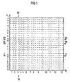
- One x-axis x and one to the x-axis x vertical y-axis y run in a surface O des Substrate S (see Fig. 1).
- Parts of the surface O, on each a memory cell is generated are each in strip-shaped, adjacent, parallel to the x-axis x running horizontal areas divided.
- the parts of the Surface O are also each in strip-shaped, adjacent, vertical ones running parallel to the y-axis Areas divided (see Fig. 1).
- Adjacent memory cells are parallel with respect to the y-axis running axes created mirror-symmetrically to each other: either first vertical areas 1 or thirteenth vertical areas 13 of these memory cells adjoin one another on. Of two each to be generated in the direction of the y-axis neighboring memory cells border a first horizontal one Area a one of the memory cells and a twenty-second horizontal area v of another of the memory cells to each other.
- third trenches G3 approximately 500 nm deep are produced by etching silicon.
- HBr + NF 3 + He + O 2 is suitable as an etchant.
- the third trenches G3 are filled with SiO 2 by depositing SiO 2 with a thickness of approx. 600 nm in a TEOS process and subsequent etching back. This creates the first insulating structures I1 (see FIG. 2).
- the first insulating structures I1 are suitable for isolating mutually complementary transistors to be produced from one another.
- the eleventh vertical area in memory cells 11 through the thirteenth vertical range 13 covered are p-doped by implantation about 2 ⁇ m deep first tubs Wa1 generated (see Fig. 2).
- n-doped second wells Wa2 approximately 2 ⁇ m deep are produced by implantation (see FIG. 2 ).
- the first insulating structures I1 thus each run between a first trough Wa1 and a second trough Wa2.
- the first troughs Wa1 and the second troughs Wa2 are strip-shaped and run essentially parallel to one another.
- the dopant concentrations of the first wells Wa1 and the second wells Wa2 are approximately 3 * 10 17 cm -3 .
- hook-shaped n-doped regions approximately 150 nm deep are produced by implantation within the first tubs Wa1.
- the dopant concentration of the hook-shaped areas is approximately 5 * 10 20 cm -3 .
- Parts of the hook-shaped regions are as second source / drain regions 1 S / D2 of first transistors, as second source / drain regions 2 S / D2 of second transistors, as second source / drain regions 5 S / D2 of fifth transistors and suitable as second source / drain regions 6 S / D2 of sixth transistors (see FIG. 2).
- the fourth mask M4 covers areas in memory cells, in which the fourteenth horizontal area n up to and including the twenty-first horizontal area u with the first vertical range 1 up to and including that fifth vertical area 5 overlap, and areas in which the fourth horizontal range d up to and including the tenth horizontal area j with the first vertical Range 1 through the fifth vertical range 5 overlap, and areas where the fourteenth horizontal range n up to and including the seventeenth horizontal area q with the sixth vertical area 6 and the seventh vertical area 7 intersect, and areas in which the fourth horizontal range d to including the seventh horizontal area g with the sixth vertical area 6 and the seventh vertical area 7 overlap, and areas where the eleventh horizontal Range k up to and including the seventeenth horizontal Area q with the eighth vertical area 8 and the ninth vertical area 9 intersect, and areas in which the first horizontal area a to inclusive the seventh horizontal area g with the eighth vertical area Intersect area 8 and the ninth vertical area 9, not starting.
- a fifth mask (not shown) made of photoresist, rectangular, approximately 150 nm deep p-doped regions are produced within the second wells Wa2.
- the dopant concentration of the rectangular areas is approx. 5 * 10 20 cm -3 .
- the p-doped regions are suitable as first source / drain regions 3 S / D1 of third transistors and first source / drain regions 4 S / D1 of fourth transistors (see FIG. 2).
- the fifth mask covers areas where the fourteenth horizontal range n through the twentieth horizontal area t with the eleventh vertical area 11 through the thirteenth vertical region 13 overlap, and areas where the third is horizontal Range c up to and including the tenth horizontal Area j with the eleventh vertical area 11 through inclusive intersect the thirteenth vertical region 13, not starting.
- a first insulating layer (not shown) is then produced by depositing SiO 2 in a thickness of approximately 100 nm.
- An approximately 100 nm thick conductive layer S1 is produced over the first insulating layer by depositing doped polysilicon.
- a second insulating layer (not shown) is produced over the conductive layer S1 by depositing SiO 2 in a thickness of approximately 100 nm (see FIG. 3).
- first trenches G1, second trenches G2 and fourth trenches G4 about 500 nm deep (see FIG. 3 ).
- the depth of the first trenches G1, the second trenches G2 and the fourth trenches G4 from the surface O is approximately 500 nm.
- the first trenches G1 and the second trenches G2 run within the first troughs Wa1.
- the fourth trenches G4 run within the second troughs Wa2.
- a second insulating structure I2 arises from the first insulating layer, and a preliminary structure VS arises from the second insulating layer.
- the sixth mask M6 in each case covers the memory cells the first vertical area 1, the sixth vertical area 6, the seventh vertical region 7 and the thirteenth vertical area 13 does not decrease.
- a seventh mask M7 made of photoresist (see Fig. 7c) and an eighth mask M8 made of photoresist (see Fig. 7d) are through oblique implantation on second flanks 1F2 of the first trenches G1 on first flanks 2F1 of the second trenches G2 and on the second Flanks 2F2 of the second trenches G2 p-doped first channel stop regions C1 generates (see Fig. 3).
- the seventh mask M7 covers in the memory cells the second tub Wa2, as well as areas where the eighteenth horizontal range r through the twentieth horizontal area t with the first vertical area 1 intersect up to and including the eighth vertical area 8, and areas where the eighth horizontal Range h up to and including the tenth horizontal range j with the first vertical range 1 up to and including that eighth vertical area 8 overlap.
- the eighth mask M8 covers the second tub Wa2 in the memory cell as well as areas in which the eighth horizontal area h up to and including the tenth horizontal area j with the first vertical area 1 and the second vertical area 2 overlap, and areas where the eighteenth horizontal range r through the twentieth horizontal area t with the first vertical area 1 and overlap the second vertical area 2, and areas in which the fourteenth horizontal area n up to and including the sixteenth horizontal area p the seventh vertical area 7 through the ninth inclusive intersect vertical area 9, and areas where the third horizontal area c up to and including the sixth horizontal area f with the seventh vertical Area 7 through the ninth vertical area 9 overlap, from.
- the ninth mask in the memory cells covers each first tubs Wa1 as well as areas where the eighteenth horizontal range r up to and including the twentieth horizontal Area t with the twelfth vertical area 12 and intersect the thirteenth vertical region 13, and Areas in which the eighth horizontal area h to including the tenth horizontal area j with the twelfth vertical area 12 and the thirteenth vertical area Overlap area 13, from.
- the first channel stop regions C1 and the second channel stop regions C2 jointly form channel stop regions C.
- the dopant concentration of the channel stop regions C is approximately 10 19 cm -3 and is greater than the dopant concentration first tubs Wa1 and the second tubs Wa2. Due to their high dopant concentration, the channel stop regions C prevent a current flow between adjacent source / drain regions.
- the tenth mask in the memory cells covers areas in which the seventeenth horizontal area q up to and including the twenty-first horizontal area u overlap with the fourth vertical area 4 up to and including the eighth vertical area 8, and areas in which the seventh horizontal area Do not overlap area g through the eleventh horizontal area k with the fourth vertical area 4 through the eighth vertical area 8.
- the diffusion areas are divided into first diffusion areas and second diffusion areas D2 (see FIG. 3).
- the first diffusion regions adjoin the second source / drain regions 1 S / D2 of the first transistors, and the second diffusion regions D2 adjoin the second source / drain regions 2 S / D2 of the second transistors.
- the dopant concentration of the diffusion areas is high and is approximately 10 20 cm -3 .
- SiO 2 is deposited in a thickness of approximately 80 nm in a TEOS process and etched back in order to on the first flanks of the first trenches G1, on the second flanks 1F2 of the first trenches G1, on the first flanks 2F1 of the second trenches G2, to produce spacers Sp on the second flanks 2F2 of the second trenches G2, on the first flanks 4F1 of the fourth trenches G4 and on the second flanks of the fourth trenches G4.
- n-doped first conductive structures L1 are produced (see FIG Fig. 3).
- the first conductive structures L1 run along the bottoms of the first trenches G1 and are connected to a first voltage connection. Parts of the first conductive structures L1 are suitable as first source / drain regions of the first transistors and as first source / drain regions 2 S / D1 of the second transistors (see FIG. 3).
- the eleventh mask M11 covers each in the memory cells the first trench G1 and areas where the fourteenth horizontal range n through the twentieth horizontal area t with the third vertical area 3 intersect up to and including the eighth vertical area 8, and rectangular areas where the third horizontal range c up to and including the tenth horizontal Area j with the third vertical area 3 through inclusive intersect the eighth vertical area 8, not starting.
- the first source / drain regions 5 are S / D1 of the fifth transistors from the first source / drain regions 6 S / D1 of the sixth transistors isolated.
- p-doped second conductive structures L2 are produced by implantation on the bottoms of the fourth trenches G4 (see FIG. 3).
- the dopant concentration of the second conductive structures L2 is approximately 5 * 10 20 cm -3 .
- the second conductive structures L2 are connected to a second voltage connection. Parts of the second conductive structure L2 are suitable as second source / drain regions of the third transistors and as second source / drain regions 4 S / D2 of the fourth transistors.
- the first source / drain regions 5 S / D1 fifth transistor When generating the first source / drain regions 5 S / D1 fifth transistor, the first source / drain regions 6 S / D1 the sixth transistors, the first conductive structures L1 and the second conductive structures L2 prevent the provisional Structure VS and the Spacer Sp the implantation of others Parts of the memory cells.
- a gate dielectric Gd is then generated by thermal oxidation (see FIG. 4).
- doped polysilicon is deposited in a thickness of approximately 40 nm and etched back to the extent that the polysilicon is arranged in the form of spacers below the flanks of the structured conductive layer S1. It is then etched with, for example, HF SiO 2 in such a way that the flanks of the structured conductive layer S1 are exposed.
- Doped polysilicon is deposited to a thickness of approximately 80 nm and etched back, causing the flanks of the first Trenches G1, the second trenches G2 and the fourth trenches G4 Spacers are created that form the structured conductive layer S1 to contact.
- Silicon is etched using a thirteenth mask M13 made of photoresist (see FIG. 7f), so that parts of the spacers are removed.
- C 2 F 6 + O 2 is suitable as an etchant. This results in first gate electrodes of the first transistors, second gate electrodes Ga2 of the second transistors, third gate electrodes of the third transistors, fourth gate electrodes Ga4 of the fourth transistors and third conductive structures L3 which are arranged on the first flanks 2F1 of the second trenches G2 (see FIG. 4 ).
- Spacers which are arranged on the second flanks 2F2 of the second trenches G2 are not etched and are suitable as word lines W. Parts of the word lines W are suitable as fifth gate electrodes Ga5 of the fifth transistors and as sixth gate electrodes of the sixth transistors.
- the thirteenth mask M13 covers in the memory cells Areas in which the fifteenth horizontal area o up to and including the seventeenth horizontal area q with the first vertical area 1 and the second vertical Area 2 overlap and areas where there is the fifteenth horizontal range up to and including the seventeenth horizontal area q with the twelfth vertical Intersect area 12 and the thirteenth vertical area 13, and areas where the first horizontal Area a through the seventh horizontal area g inclusive with the first vertical area 1 and the second vertical Overlap area 2 and areas where the first horizontal area a through the fourth horizontal Area d with the third vertical area 3 to including the sixth vertical area 6 overlap, and areas where the first horizontal area a up to and including the seventh horizontal area g with the twelfth vertical region 12 and the thirteenth overlap vertical area 13, not from.
- first horizontal conductive structures H1, second horizontal conductive structures H2, third horizontal conductive structures, fourth horizontal conductive structures H4 and fifth horizontal ones are produced by etching silicon from the structured conductive layer S1 conductive structures H5 (see Fig. 4, 6b, 6d).
- C 2 F 6 + O 2 is suitable as an etchant.
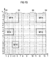
- the fourteenth mask M14 covers areas in which the eighteenth horizontal range r up to and including the twenty-second horizontal area v with the first vertical Ranges 1 through the sixth vertical Overlap area 6 and areas where the twelfth horizontal range 1 through the fourteenth inclusive horizontal area n with the first vertical area 1 through the fourth vertical region 4 overlap, and areas where the eighteenth is horizontal R ranges up to and including the twenty-second horizontal area v with the eleventh vertical area 11 up to and including the thirteenth vertical region 13 overlap, and areas where the twelfth horizontal Range 1 through the fourteenth horizontal Area n with the eleventh vertical area 11 through inclusive intersect the thirteenth vertical region 13, and areas in which the fifth horizontal area e up to and including the eighth horizontal area h with the fourth vertical range 4 up to and including that overlap the sixth vertical area 6.
- the first horizontal conductive structures H1 adjoin the first Gate electrodes Ga1 of the first transistors and to the third conductive structures L3.
- the second horizontal conductive Structures H2 adjoin the second gate electrodes Ga2 of the second transistors.
- the third horizontal conductive structures adjoin the third gate electrodes Ga3 of the third transistors.
- the fourth horizontal conductive structures H4 adjoin the fourth gate electrodes Ga4 of the fourth transistor.
- the fifth horizontal conductive structures H5 adjoin the third conductive ones Structures L3.
- SiO 2 is deposited to a thickness of approximately 600 nm.
- 500 nm of SiO 2 is removed and planarized, which creates a third insulating structure I3 (see FIG. 5).
- second contacts K2 which contact the second source / drain regions 1 S / D2 of the first transistors
- fourth contacts which contact the first source / drain regions 3 S / D1 of the third transistors
- fifth contacts K5 contacting the second source / drain regions 2 S / D2 of the second transistors
- sixth contacts contacting the first source / drain regions 4 S / D1 of the fourth transistors is made of photoresist using a fifteenth mask (not shown) SiO 2 selectively etched to silicon until parts of the source / drain regions are exposed.
- CHF 3 + O 2 is suitable as an etchant.
- the fifteenth mask in each case covers the memory cells Areas in which the thirteenth horizontal area m up to and including the fifteenth horizontal area o the second vertical area 2 through the fourth inclusive vertical area 4 intersect, and areas where the fifth horizontal area e up to and including the eighth horizontal area h with the third vertical Range 3 through the fifth vertical range 5 overlap, and areas where the thirteenth horizontal Range m up to and including the fifteenth horizontal Area o with the twelfth vertical area 12 overlap, and areas where the third is horizontal Range c up to and including the sixth horizontal Intersect area f with the twelfth vertical area 12, not starting.
- tungsten is deposited to a thickness of approximately 200 nm, which results in the second contacts K2, the fourth contacts K4, the fifth contacts K5 and the sixth contacts (see FIGS. 5, 6b).
- a sixteenth mask M16 made of photoresist is used to etch tungsten, which results in fifth conductive structures L5 and sixth conductive structures L6 (see FIGS. 5, 6b).
- SF 6 for example, is suitable as an etchant.
- the fifth conductive structures L5 each adjoin a second contact K2 and a fourth contact K4.
- the sixth conductive structures L6 each adjoin a fifth contact K5 and a sixth contact.
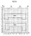
- the sixteenth mask M16 covers in the memory cells a first U-shaped area and a second U-shaped Range.
- the first U-shaped area consists of Areas in which the thirteenth horizontal area m up to and including the seventeenth horizontal area q the second vertical area 2 through the fourth inclusive vertical area 4 intersect, and areas where the fifteenth horizontal range o up to and including the seventeenth horizontal area q with the fifth vertical range 5 through the eleventh vertical Area 11 overlap and areas where the thirteenth horizontal range m up to and including the seventeenth horizontal area q with the twelfth vertical area 12 overlap.
- the second U-shaped area exists from areas in which the fourth horizontal area d up to and including the ninth horizontal area i with the third vertical area 3 through the fifth vertical area 5 intersect, and areas where the seventh horizontal range g up to and including the ninth horizontal area i with the sixth vertical area 6 up to and including the eleventh vertical region 11 overlap, and areas where the third is horizontal Range c up to and including the ninth horizontal Overlap area i with the twelfth vertical area 12.
- Boron phosphor glass is deposited in a thickness of approx. 600 nm. With the help of chemical-mechanical polishers, the borophosphorus glass is planarized, which creates a fourth insulating structure I4 (see FIG. 6a).
- first contacts K1 which contact the second source / drain regions 1 S / D2 of the first transistors
- third contacts which contact the first source / drain regions 3 S / D1 of the third transistors
- seventh contacts K7 contacting the second source / drain regions 5 S / D2 of the fifth transistor
- eighth contacts contacting the second source / drain regions 6 S / D2 of the sixth transistors is carried out using a seventeenth mask (not shown)
- Photoresist borophosphorus glass is selectively etched to silicon until parts of the source / drain regions are exposed.
- C 2 F 6 + O 2 is suitable as an etchant.
- the seventeenth mask in each case covers the memory cells Areas in which the nineteenth horizontal area s up to and including the twenty-first horizontal area u with the second vertical area 2 up to and including that fourth vertical area 4 intersect, and areas in which are the nineteenth horizontal range s up to and including the twenty-first horizontal area u with overlap the twelfth vertical area 12, and areas in which the eleventh horizontal range k up to and including the thirteenth horizontal area m with the ninth vertical area 9 intersect, and areas in which the second horizontal area b up to and including fifth horizontal area e with the ninth vertical area 9 overlap, not off.
- tungsten is in 300 nm thick and etched back, whereby the first contacts K1, the third contacts, the seventh Contacts K7 and the eighth contacts are created (see Fig. 6b, 6d).
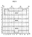
- AlSiCu is deposited in a thickness of approx. 500 nm and structured with an eighteenth mask M18 made of photoresist (see FIG. 7i) by an etching step.
- BCl 3 + Cl 2 + N 2 + CH 4 is suitable as an etchant.
- a fourth conductive structure L4 adjoins a first contact K1 and a third contact.
- the first bit lines B1 are strip-shaped, run perpendicular to the first trenches G1 and adjoin the seventh contacts K7.
- the second bit lines B2 are essentially strip-shaped, run parallel to the first bit lines B1 and adjoin the eighth contacts.
- the eighteenth mask M18 in the memory cells covers Areas in which the seventeenth horizontal area q up to and including the twenty-first horizontal Area u with the second vertical area 2 through inclusive intersect the fourth vertical area 4, and areas in which the seventeenth horizontal area q up to and including the nineteenth horizontal area s with the fifth vertical range 5 up to and including that eleventh vertical area 11 overlap, and areas in which are the seventeenth horizontal range q up to and including the twenty-first horizontal area u with intersect the twelfth vertical region 12, the eleventh horizontal area k, the twelfth horizontal area 1, the thirteenth horizontal area m, the fourth horizontal area Area d, the fifth horizontal area e, the sixth horizontal area f, the seventh horizontal area g and areas where the second horizontal Area b and the third horizontal area c with the ninth intersect vertical area 9, from.
- the dimensions of the layers, areas, areas and trenches described can be adapted to the respective requirements.
- Structures and layers made of SiO 2 can be produced in particular by thermal oxidation or by a deposition process.
- Polysilicon can be doped both during and after the deposition.
- doped polysilicon for example, metal silicides and / or metals can also be used.
- metal silicides and / or metals can also be used.
Description
- Figur 1
- zeigt einen eine Speicherzelle umfassenden Ausschnitt aus einer Oberfläche eines Substrats. Die Oberfläche ist in horizontale Bereiche und in vertikale, die horizontalen Bereiche überlappende Bereiche unterteilt.
- Figur 2
- zeigt einen Querschnitt entlang einer Grenzlinie eines siebten horizontalen Bereichs und eines achten horizontalen Bereichs durch das Substrat, nachdem erste isolierende Strukturen, erste dotierte Wannen, zweite dotierte Wannen, erste Source/Drain-Gebiete von vierten Transistoren, zweite Source/Drain-Gebiete von zweiten Transistoren, zweite Source/Drain-Gebiete von ersten Transistoren, erste Source/Drain-Gebiete von dritten Transistoren, zweite Source/Drain-Gebiete von fünften Transistoren und zweite Source/Drain-Gebiete von sechsten Transistoren erzeugt wurden.
- Figur 3
- zeigt den Querschnitt aus Figur 2, nachdem eine zweite isolierende Struktur, eine leitende Schicht, eine vorläufige Struktur, erste Gräben, zweite Gräben, vierte Gräben, Channel/Stop-Gebiete, Diffusionsgebiete, Spacer, erste leitende Strukturen, erste Source/Drain-Gebiete der ersten Transistoren, erste Source/Drain-Gebiet der zweiten Transistoren, erste Source/Drain-Gebiete der fünften Transistoren, erste Source/Drain-Gebiete der sechsten Transistoren, zweite leitende Strukturen, zweite Source/Drain-Gebiete der dritten Transistoren und zweite Source/Drain-Gebiete der vierten Transistoren erzeugt wurden.
- Figur 4
- zeigt den Querschnitt aus Figur 3, nachdem ein Gatedielektrikum, Gateelektroden, dritte leitende Strukturen und horizontale leitende Strukturen erzeugt wurden.
- Figur 5
- zeigt den Querschnitt aus Figur 4, nachdem zweite Kontakte, vierte Kontakte, fünfte Kontakte, sechste Kontakte, fünfte leitende Strukturen, sechste leitende Strukturen und eine dritte isolierende Struktur erzeugt wurden.
- Figur 6a
- zeigt den Querschnitt aus Figur 5, nachdem eine vierte isolierende Struktur, erste Kontakte, dritte Kontakte, siebte Kontakte, achte Kontakte, vierte leitende Strukturen, erste Bitleitungen und zweite Bitleitungen erzeugt wurden.
- Figur 6b
- zeigt das Substrat aus Figur 6a in einem zum Querschnitt aus Figur 6a parallelen Querschnitt entlang der einer Grenzlinie zwischen einem dreizehnten horizontalen Bereich und einem vierzehnten horizontalen Bereich.
- Figur 6c
- zeigt das Substrat aus Figur 6a in einem zum Querschnitt aus Figur 6a parallelen Querschnitt entlang eines zwölften horizontalen Bereichs.
- Figur 6d
- zeigt einen zum Querschnitt aus Figur 6a senkrechten Querschnitt durch das Substrat aus Figur 6a entlang eines dritten vertikalen Bereichs.
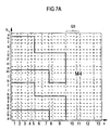
- Figur 7a
- zeigt den Ausschnitt aus Figur 1, nachdem die ersten isolierenden Strukturen in Form von mit isolierendem Material gefüllten dritten Gräben erzeugt wurden. Auf die Oberfläche wurde eine vierte Maske aufgebracht.
- Figur 7b
- zeigt den Ausschnitt aus Figur 7a, nachdem mit Hilfe einer sechsten Maske die ersten Gräben, die zweiten Gräben und die vierten Gräben erzeugt wurden.
- Figur 7c
- zeigt den Ausschnitt aus Figur 7b. Auf die Oberfläche wurde eine siebte Maske aufgebracht.
- Figur 7d
- zeigt den Ausschnitt aus Figur 7c. Auf die Oberfläche wurde eine achte Maske aufgebracht.
- Figur 7e
- zeigt den Ausschnitt aus Figur 7d. Auf die Oberfläche wurde eine elfte Maske aufgebracht.
- Figur 7f
- zeigt den Ausschnitt aus Figur 7e. Auf die Oberfläche wurde eine dreizehnte Maske aufgebracht.
- Figur 7g
- zeigt den Ausschnitt aus Figur 7f. Auf die Oberfläche wurde eine vierzehnte Maske aufgebracht.
- Figur 7h
- zeigt den Ausschnitt aus Figur 7g. Auf die Oberfläche wurde eine sechzehnte Maske aufgebracht.
- Figur 7i
- zeigt den Ausschnitt aus Figur 7h. Auf die Oberfläche wurde eine achtzehnte Maske aufgebracht.
Claims (10)
- SRAM-Zellenanordnung,mit Speicherzellen, die jeweils 6 Transistoren umfassen,bei der ein erstes Source/Drain-Gebiet (1 S/D1) eines ersten der Transistoren mit einem ersten Source/Drain-Gebiet (2 S/D1) eines zweiten der Transistoren und einem ersten Spannungsanschluß verbunden ist,bei der ein zweites Source/Drain-Gebiet (1 S/D2) des ersten Transistors mit einem ersten Source/Drain-Gebiet (3 S/D1) eines dritten der Transistoren, einem ersten Source/Drain-Gebiet (5 S/D1) eines fünften der Transistoren, einer Gateelektrode (Ga2) des zweiten Transistors und einer Gateelektrode (Ga4) eines vierten der Transistoren verbunden ist,bei der eine Gateelektrode (Ga1) des ersten Transistors mit einem zweiten Source/Drain-Gebiet (2 S/D2) des zweiten Transistors, einem ersten Source/Drain-Gebiet (4 S/D1) des vierten Transistors, einer Gateelektrode (Ga3) des dritten Transistors und einem ersten Source/Drain-Gebiet (6 S/D1) eines sechsten der Transistoren verbunden ist,bei der ein zweites Source/Drain-Gebiet (3 S/D2) des dritten Transistors mit einem zweiten Source/Drain-Gebiet (4 S/D2) des vierten Transistors und einem zweiten Spannungsanschluß verbunden ist,bei der ein zweites Source/Drain-Gebiet (5 S/D2) des fünften Transistors mit einer ersten Bitleitung (B1) verbunden ist,bei der eine Gateelektrode (Ga5) des fünften Transistors mit einer Gateelektrode (Ga6) des sechsten Transistors und mit einer Wortleitung (W) verbunden ist,bei der ein zweites Source/Drain-Gebiet (6 S/D2) des sechsten Transistors mit einer zweiten Bitleitung (B2) verbunden ist,bei der der dritte Transistor und der vierte Transistor komplementär zum ersten Transistor, zum zweiten Transistor, zum fünften Transistor und zum sechsten Transistor sind,bei der die sechs Transistoren als vertikale MOS-Transistoren ausgebildet sind,bei der der erste Transistor und der zweite Transistor an einer zweiten Flanke (1F2) eines ersten Grabens (G1), der in einem Substrat (S) verläuft, angeordnet sind,bei der der fünfte Transistor und der sechste Transistor an einer zweiten Flanke (2F2) eines zweiten Grabens (G2), der in dem Substrat (S) und parallel zum ersten Graben (G1) verläuft, angeordnet sind,bei der der dritte Transistor und der vierte Transistor an einer ersten Flanke (4F1) eines vierten Grabens (G4), der in dem Substrat (S) und parallel zum zweiten Graben (G2) verläuft, angeordnet sind,bei der die Wortleitung (W) entlang der zweiten Flanke (2F2) des zweiten Grabens (G2) verläuft,bei der eine erste leitende Struktur (L1) mit dem ersten Spannungsanschluß und eine zweite leitende Struktur (L2) mit dem zweiten Spannungsanschluß verbunden sind,bei der die erste leitende Struktur (L1) entlang des ersten Grabens (G1) und die zweite leitende Struktur (L2) entlang des vierten Grabens (G4) verlaufen,bei der die erste Bitleitung (B1) und die zweite Bitleitung (B2) quer zu der Wortleitung (W) und parallel zueinander verlaufen,bei der das erste Source/Drain-Gebiet (1 S/D1) des ersten Transistors und das erste Source/Drain-Gebiet (2 S/D1) des zweiten Transistors mit der ersten leitenden Struktur (L1) verbunden sind,bei der das zweite Source/Drain-Gebiet (3 S/D2) des dritten Transistors und das zweite Source/Drain-Gebiet (4 S/D2) des vierten Transistors mit der zweiten leitenden Struktur (L2) verbunden sind.
- SRAM-Zellenanordnung nach Anspruch 1, bei der Gateelektroden oder leitende Strukturen an außerhalb des ersten Grabens (G1), des zweiten Grabens (G2) und des vierten Grabens (G4) oberhalb einer Oberfläche (O) des Substrats (S) angeordnete horizontale leitende Strukturen angrenzen, über die sie kontaktiert sind.
- SRAM-Zellenanordnung nach Anspruch 2,bei der der erste Graben (G1) und der zweite Graben (G2) in einer von einem zweiten Leitfähigkeitstyp dotierten ersten Wanne (Wa1) des Substrats (S) angeordnet sind,bei der der vierte Graben (G4) in einer von einem ersten, zum zweiten Leitfähigkeitstyp entgegensetzten Leitfähigkeitstyp dotierten zweiten Wanne (Wa2) des Substrats (S) angeordnet ist,bei der die erste leitende Struktur (L1) innerhalb des Substrats (S) an einen Boden des ersten Grabens (G1) angrenzt und vom ersten Leitfähigkeitstyp dotiert ist, und die zweite leitende Struktur innerhalb des Substrats (S) an einen Boden des vierten Grabens (G4) angrenzt und vom zweiten Leitfähigkeitstyp dotiert ist,bei der das erste Source/Drain-Gebiet (1 S/D1) des ersten Transistors und das erste Source/Drain-Gebiet (2 S/D1) des zweiten Transistors Teile der ersten leitenden Struktur (L1) sind,bei der das zweite Source/Drain-Gebiet (3 S/D2) des dritten Transistors und das zweite Source/Drain-Gebiet (4 S/D2) des vierten Transistors Teile der zweiten leitenden Struktur (L2) sind,bei der zwischen horizontalen leitenden Strukturen (H1, H2, H4, H5) und der Oberfläche (O) Teile einer zweiten isolierenden Struktur (I2) angeordnet sind,bei der die Gateelektrode (Gal) des ersten Transistors, die Gateelektrode (Ga2) des zweiten Transistors, die Gateelektrode (Ga3) des dritten Transistors, die Gateelektrode (Ga4) des vierten Transistors, die Gateelektrode (Ga5) des fünften Transistors und die Gateelektrode (Ga6) des sechsten Transistors als Spacer ausgebildet sind,bei der die Gateelektrode (Ga1) des ersten Transistors an eine erste horizontale leitende Struktur (H1), die Gateelektrode (Ga2) des zweiten Transistors an eine zweite horizontale leitende Struktur (H2), die Gateelektrode (Ga3) des dritten Transistors an eine dritte horizontale leitende Struktur und die Gateelektrode (Ga4) des vierten Transistors an eine vierte horizontale leitende Struktur (H4) angrenzt,bei der die Wortleitung (W) als Spacer an der zweiten Flanke (2F2) des zweiten Grabens (G2) ausgebildet ist,bei der die Gateelektrode (Ga5) des fünften Transistors und die Gateelektrode (Ga6) des sechsten Transistors Teile der Wortleitung (W) sind,bei der eine dritte leitende Struktur (L3) als Spacer an der ersten Flanke (2F1) des zweiten Grabens (G2) ausgebildet ist,bei der die dritte leitende Struktur (L3) an die erste horizontale leitende Struktur (H1) und an die fünfte horizontale leitende Struktur (H5) angrenzt,bei der die zweite Flanke (1F2) des ersten Grabens (G1), die erste Flanke (2F1) des zweiten Grabens (G2), die zweite Flanke (2F2) des zweiten Grabens (G2) und die erste Flanke (4F1) des vierten Grabens (G4) mit einem Gatedielektrikum (Gd) versehen sind,bei der das zweite Source/Drain-Gebiet (1 S/D2) des ersten Transistors und das zweite Source/Drain-Gebiet (2 S/D2) des zweiten Transistors an die Oberfläche (O) sowie an die zweite Flanke (1F2) des ersten Grabens (G1) und an die erste Flanke (2F1) des zweiten Grabens (G2) angrenzen,bei der das erste Source/Drain-Gebiet (3 S/D1) des dritten Transistors und das erste Source/Drain-Gebiet (4 S/D1 des vierten Transistors an die Oberfläche (O) sowie an die erste Flanke (4 F1) des vierten Grabens (G4) angrenzen,bei der das zweite Source/Drain-Gebiet (5 S/D2) des fünften Transistors und das zweite Source/Drain-Gebiet (6 S/D2) des sechsten Transistors an die Oberfläche (O) sowie an die zweite Flanke (2F2) des zweiten Grabens (G2) angrenzen,bei der die erste horizontale leitende Struktur (H1) über einen ersten Kontakt (K1) mit einer vierten leitenden Struktur (L4) verbunden ist,bei der die dritte horizontale leitende Struktur über einen dritten Kontakt (K3) mit der vierten leitenden Struktur (L4) verbunden ist,bei der die vierte leitende Struktur (L4) oberhalb der zweiten horizontalen leitenden Strukturen (H1, H2, H4, H5) angeordnet ist,bei der das zweite Source/Drain-Gebiet (1 S/D2) des ersten Transistors über einen zweiten Kontakt (K2) mit der zweiten horizontalen leitenden Struktur (H2) und einer fünften leitenden Struktur (L5) verbunden ist,bei der die fünfte leitende Struktur (L5) oberhalb der horizontalen leitenden Strukturen (H1, H2, H4, H5) und unterhalb der vierten leitenden Struktur (L4) angeordnet ist,bei der das erste Source/Drain-Gebiet (3 S/D1) des dritten Transistors über einen vierten Kontakt (K4) mit der vierten horizontalen leitenden Struktur (H4) und der fünften leitenden Struktur (L5) verbunden ist,bei der das zweite Source/Drain-Gebiet (2 S/D2) des zweiten Transistors über einen fünften Kontakt (K5) mit der fünften horizontalen leitenden Struktur (H5) und einer sechsten leitenden Struktur (L6) verbunden ist,bei der die Höhe der sechsten leitenden Struktur (L6) bezüglich einer Achse senkrecht zur Oberfläche (O) der Höhe der fünften leitenden Struktur (L5) entspricht,bei der das erste Source/Drain-Gebiet (4 S/D1) des vierten Transistors über einen sechsten Kontakt (K6) mit der sechsten leitenden Struktur (L6) verbunden ist,bei der das zweite Source/Drain-Gebiet (5 S/D2) des fünften Transistors über einen siebten Kontakt (K7) mit der ersten Bitleitung (B1) und das zweite Source/Drain-Gebiet (6 S/D2) des sechsten Transistors über einen achten Kontakt (K8) mit der zweiten Bitleitung (B2) verbunden sind,bei der ein vom ersten Leitfähigkeitstyp dotierter erster Diffusionsbereich innerhalb des Substrats (S) an die erste Flanke (2F1) des zweiten Grabens (G2), an das zweite Source/Drain-Gebiet (1 S/D1) des ersten Transistors und an das erste Source/Drain-Gebiet (5 S/D1) des fünften Transistors angrenzt,bei der ein vom ersten Leitfähigkeitstyp dotierter zweiter Diffusionsbereich (D2) innerhalb des Substrats (S) an die erste Flanke (2F1) des zweiten Grabens (G2), an das zweite Source/Drain-Gebiet (2 S/D2) des zweiten Transistors und an das erste Source/Drain-Gebiet (6 S/D1) des sechsten Transistors angrenzt.
- SRAM-Zellenanordnung nach den Ansprüchen 1, 2 und/oder 3,bei der innerhalb des Substrats (S) an Teilen der Flanken der Gräben an denen keine Gateelektroden und keine Diffusionsbereiche angrenzen, hochdotierte Channel-Stop-Gebiete (C) angeordnet sind,bei der eine streifenförmige erste Isolationsstruktur (I1) parallel zu und zwischen dem zweiten Graben (G2) und dem vierten Graben (G4) verläuft.
- SRAM-Zellenanordnung nach einem der Ansprüche 1 bis 4, bei der entlang der ersten Bitleitung (B1) benachbarte Speicherzellen bezüglich einer Achse, die entlang einer Mittellinie eines ersten Grabens (G1) oder eines vierten Grabens (G4) verläuft, spiegelsymmetrisch zueinander angeordnet sind.
- Verfahren zur Herstellung einer SRAM-Zellenanordnung,bei dem Speicherzellen, die jeweils einen ersten Transistor, einen zweiten Transistor, einen dritten Transistor, einen vierten Transistor, einen fünften Transistor und einen sechsten Transistor umfassen, erzeugt werden,bei dem Wortleitungen (W), erste Bitleitungen (B1) und zweite Bitleitungen (B2) erzeugt werden,bei dem Gateelektroden, erste Source/Drain-Gebiete und zweite Source/Drain-Gebiete erzeugt werden,bei dem ein erstes Source/Drain-Gebiete (1 S/D1) des ersten Transistors mit einem ersten Source/Drain-Gebiet (2 S/D1) des zweiten Transistors und einem ersten Spannungsanschluß verbunden wird,bei dem ein zweites Source/Drain-Gebiet (1 S/D2) des ersten Transistors mit einem ersten Source/Drain-Gebiet (3 S/D1) des dritten Transistors, einem ersten Source/Drain-Gebiet (5 S/D1) des fünften Transistors, einer Gateelektrode (Ga2) des zweiten Transistors und einer Gateelektrode (Ga4) des vierten Transistors verbunden wird,bei dem eine Gateelektrode (Ga1) des ersten Transistors mit einem zweiten Source/Drain-Gebiet (2 S/D2) des zweiten Transistors, einem ersten Source/Drain-Gebiet (4 S/D1) des vierten Transistors, einer Gateelektrode (Ga3) des dritten Transistors und einem ersten Source/Drain-Gebiet (6 S/D1) eines sechsten Transistors verbunden wird,bei dem ein zweites Source/Drain-Gebiet (3 S/D2) des dritten Transistors mit einem zweiten Source/Drain-Gebiet (4 S/D2) des vierten Transistors und einem zweiten Spannungsanschluß verbunden wird,bei dem ein zweites Source/Drain-Gebiet (5 S/D2) des fünften Transistors mit einer ersten Bitleitung (B1) verbunden wird,bei dem eine Gateelektrode (Ga5) des fünften Transistors mit einer Gateelektrode (Ga6) des sechsten Transistors und mit einer Wortleitung (W) verbunden wird,bei dem ein zweites Source/Drain-Gebiet (6 S/D2) des sechsten Transistors mit einer zweiten Bitleitung (B2) verbunden wird,bei dem der dritte Transistor und der vierte Transistor als zum ersten Transistor, zum zweiten Transistor, zum fünften Transistor und zum sechsten Transistor komplementäre Transistoren ausgebildet werden,bei dem die sechs Transistoren als vertikale MOS-Transistoren gebildet werden,bei dem in einem Substrat (S) erste Gräben (G1), zweite Gräben (G2) und vierte Gräben (G4), die im wesentlichen parallel zueinander verlaufen, erzeugt werden,bei dem Flanken der ersten Gräben (G1), der zweiten Gräben (G2) und der vierten Gräben (G4) mit einem Gatedielektrikum (Gd) versehen werden,bei dem der erste Transistor und der zweite Transistor an eine zweite Flanke (1F2) eines ersten Grabens (G1) angrenzend gebildet werden,bei dem der fünfte Transistor und der sechste Transistor an eine zweite Flanke (2F2) eines zweiten Grabens (G2) angrenzend gebildet werden,bei dem der dritte Transistor und der vierte Transistor an eine erste Flanke (4F1) eines viertes Grabens (G4) angrenzend gebildet werden,bei dem die Wortleitung (W) entlang der zweiten Flanke (2F2) des zweiten Grabens (G2) gebildet wird,bei dem entlang des ersten Grabens (G1) eine erste leitende Struktur (L1) gebildet wird, die mit dem ersten Spannungsanschluß verbunden wird,bei dem entlang des vierten Grabens (G4) eine zweite leitende Struktur (L2) erzeugt wird, die mit dem zweiten Spannungsanschluß verbunden wird,bei dem quer zu der Wortleitung (W) die erste Bitleitung (B1) und parallel zur ersten Bitleitung (B1) die zweite Bitleitung (B2) gebildet werden,bei dem das erste Source/Drain-Gebiet (1 S/D1) des ersten Transistors und das erste Source/Drain-Gebiet (2 S/D1) des zweiten Transistors mit der ersten leitenden Struktur (L1) verbunden werden,bei dem das zweite Source/Drain-Gebiet (3 S/D2) des dritten Transistors und das zweite Source/Drain-Gebiet (4 S/D2) des vierten Transistors mit der zweiten leitenden Struktur (L2) verbunden werden.
- Verfahren nach Anspruch 6, bei der zur Kontaktierung von Gateelektroden oder leitenden Strukturen außerhalb des ersten Grabens (G1), des zweiten Grabens (G2) und des vierten Grabens (G4) oberhalb einer Oberfläche (O) des Substrats (S) horizontale leitende Strukturen erzeugt werden, so, daß die horizontalen leitenden Strukturen jeweils an eine Gateelektrode oder/und eine leitende Struktur angrenzen.
- Verfahren nach Anspruch 7,bei dem an der Oberfläche (O) durch Implantation das zweite Source/Drain-Gebiet (1 S/D2) des ersten Transistors, das zweite Source/Drain-Gebiet (2 S/D2) des zweiten Transistors, das zweite Source/Drain-Gebiet (5 S/D2) des fünften Transistors, das zweite Source/Drain-Gebiet (6 S/D2) des sechsten Transistors, das erste Source/Drain-Gebiet (3 S/D1) des dritten Transistors und das erste Source/Drain-Gebiet (4 S/D1) des vierten Transistors erzeugt werden,bei dem anschließend die ersten Gräben (G1) die zweiten Gräben (G2) und die vierten Gräben (G4) erzeugt werden,bei dem das zweite Source/Drain-Gebiet (1 S/D2) des ersten Transistors, das zweite Source/Drain-Gebiet (2 S/D2) des zweiten Transistors, das zweite Source/Drain-Gebiet (5 S/D2) des fünften Transistors, das zweite Source/Drain-Gebiet (6 S/D2) des sechsten Transistors, das erste Source/Drain-Gebiet (3 S/D1) des dritten Transistors und das erste Source/Drain-Gebiet (4 S/D1) des vierten Transistors, die ersten Gräben (G1), die zweiten Gräben (G2) und die vierten Gräben (G4) so erzeugt werden, daß das zweite Source/Drain-Gebiet (1 S/D2) des ersten Transistors und das zweite Source/Drain-Gebiet (2 S/D2) des zweiten Transistors an die zweite Flanke (1F2) des ersten Grabens (G1) und an die erste Flanke (2F1) des zweiten Grabens (G2) angrenzen und so, daß das zweite Source/Drain-Gebiet (5 S/D2) des fünften Transistors und das zweite Source/Drain-Gebiet (6 S/D2) des sechsten Transistors an die zweite Flanke (2F2) des zweiten Grabens (G2) angrenzen, und so, daß das erste Source/Drain-Gebiet (3 S/D1) des dritten Transistors und das erste Source/Drain-Gebiet (4 S/D1) des vierten Transistors an die erste Flanke (4F1) des vierten Grabens (4) angrenzen,bei dem angrenzend an das zweite Source/Drain-Gebiet (1 S/D2) des ersten Transistors an der ersten Flanke (2F1) des zweiten Grabens (G2) innerhalb des Substrats (S) durch schräge Implantation ein erster Diffusionsbereich erzeugt wird,bei dem angrenzend an das zweite Source/Drain-Gebiet (2 S/D2) des zweiten Transistors an der ersten Flanke (2F1) des zweiten Grabens (G2) innerhalb des Substrats (S) durch schräge Implantation ein zweiter Diffusionsbereich (D2) erzeugt wird,bei dem durch Implantation innerhalb des Substrats (S) die von einem ersten Leitfähigkeitstyp dotierte erste leitende Struktur (L1) an einem Boden des ersten Grabens (G1) erzeugt wird,bei dem durch Implantation an einem Boden des zweiten Grabens (G2) das erste Source/Drain-Gebiet (5 S/D1) des fünften Transistors und das erste Source/Drain-Gebiet (6 S/D1) des sechsten Transistors erzeugt werden,bei dem durch Implantation an einem Boden des vierten Grabens (G4) von einem zweiten, zum ersten Leitfähigkeitstyp entgegengesetzten zweite Leitfähigkeitstyp dotierte zweite dotierte leitende Struktur (L2) erzeugt wird,bei dem durch Abscheiden, Rückätzen und maskiertes Ätzen von leitendem Material an der zweiten Flanke (2F2) des zweiten Grabens (G2) die Wortleitung (W), an der zweiten Flanke (1F2) des ersten Grabens (G1) die Gateelektrode (Ga1) des ersten Transistors und die Gateelektrode (Ga2) des zweiten Transistors, an der ersten Flanke (2F1) des zweiten Grabens (G2) eine dritte leitende Struktur (L3) und an der ersten Flanke (4F1) des vierten Grabens (G4) die Gateelektrode (Ga3) des dritten Transistors und die Gateelektrode (Ga4) des vierten Transistors erzeugt werden,bei dem durch Abscheiden von isolierendem Material auf die Oberfläche (O) eine zweite isolierende Struktur (I2) erzeugt wird,bei dem durch Abscheiden von leitendem Material auf die zweite isolierende Struktur (I2) eine leitende Schicht (S1) gebildet wird,bei dem durch Ätzen von leitenden Material mit Hilfe einer vierzehnten Maske (M14) eine erste horizontale leitende Struktur (H1), eine zweite horizontale leitende Struktur (H2), eine dritte horizontale leitende Struktur, eine vierte horizontale leitende Struktur (H4) und eine fünfte horizontale leitende Struktur (H5) erzeugt werden,bei dem durch Abscheiden und Rückätzen von isolierendem Material eine dritte isolierende Struktur (I3) erzeugt wird,bei dem ein zweiter Kontakt (K2), der an das zweite Source/Drain-Gebiet (1 S/D2) des ersten Transistors angrenzt, ein fünfter Kontakt (K5), der an das zweite Source/Drain-Gebiet (2 S/D2) des zweiten Transistors angrenzt, ein vierter Kontakt (K4), der an das erste Source/Drain-Gebiet (3 S/D1) des dritten Transistors angrenzt, ein sechster Kontakt (K6), der an das erste Source/Drain-Gebiet (4 S/D1) des vierten Transistors angrenzt, eine fünfte leitende Struktur (L5), die an den zweiten Kontakt (K2) und an den vierten Kontakt (K4) angrenzt und eine sechste leitende Struktur (L6), die an den fünften Kontakt (K5) und an den sechsten Kontakt (K6) angrenzt, erzeugt werden, indem mit Hilfe einer fünfzehnten Maske (M15) isolierendes Material geätzt und anschließend leitendes Material abgeschieden und mit Hilfe einer sechzehnten Maske (M16) strukturiert wird,bei dem durch Abscheiden und Rückätzen von isolierendem Material eine vierte isolierende Struktur (I4) erzeugt wird,bei dem ein erster Kontakt (K1), der an die erste horizontale leitende Struktur (H1) angrenzt, ein dritter Kontakt (K3), der an die dritte horizontale leitende Struktur angrenzt, ein siebter Kontakt (K7), der an das zweite Source/Drain-Gebiet (5 S/D2) des fünften Transistors angrenzt, ein achter Kontakt (K8), der an das zweite Source/Drain-Gebiet (6 S/D2) des sechsten Transistors angrenzt, eine vierte leitende Struktur (L4), die an den ersten Kontakt (K1) und an den dritten Kontakt (K3) angrenzt, eine erste Bitleitung (B1), die an den siebten Kontakt (K7) angrenzt und eine zweite Bitleitung (B2), die an den achten Kontakt (K8) angrenzt, erzeugt werden, indem mit Hilfe einer siebzehnten Maske (M17) isolierendes Material geätzt wird und anschließend leitendes Material abgeschieden und mit Hilfe einer achtzehnten Maske (M18) strukturiert wird.
- Verfahren nach den Ansprüchen 6, 7 und/oder 8,bei dem parallel zueinander laufende dritte Gräben (G3) erzeugt und mit isolierendem Material gefüllt werden, wodurch erste isolierende Strukturen (I1) erzeugt werden,bei dem der zweite Graben (G2) und der vierte Graben (G4) so erzeugt werden, daß sie parallel zum dritten Graben (G3) verlaufen, und daß der dritte Graben (G3) zwischen ihnen liegt,bei dem durch schräge Implantation hochdotierte Channel-Stop Gebiete (C) an Teilen der Flanken der Gräben, an die keine Gateelektroden und keine Diffusionsbereiche angrenzen, erzeugt werden.
- Verfahren nach einem der Ansprüche 6 bis 9, bei dem entlang der ersten Bitleitung (B1) benachbarte Speicherzellen spiegelsymmetrisch zueinander bezüglich einer Achse, die entlang einer Mittellinie eines ersten Grabens (G1) oder eines vierten Grabens (G4) verläuft, erzeugt werden.
Applications Claiming Priority (3)
| Application Number | Priority Date | Filing Date | Title |
|---|---|---|---|
| DE19727472 | 1997-06-27 | ||
| DE19727472 | 1997-06-27 | ||
| PCT/DE1998/001551 WO1999000847A1 (de) | 1997-06-27 | 1998-06-05 | Sram-zellenanordnung und verfahren zu deren herstellung |
Publications (2)
| Publication Number | Publication Date |
|---|---|
| EP0992068A1 EP0992068A1 (de) | 2000-04-12 |
| EP0992068B1 true EP0992068B1 (de) | 2003-09-03 |
Family
ID=7833897
Family Applications (1)
| Application Number | Title | Priority Date | Filing Date |
|---|---|---|---|
| EP98934869A Expired - Lifetime EP0992068B1 (de) | 1997-06-27 | 1998-06-05 | Sram-zellenanordnung und verfahren zu deren herstellung |
Country Status (6)
| Country | Link |
|---|---|
| US (2) | US6222753B1 (de) |
| EP (1) | EP0992068B1 (de) |
| JP (1) | JP2002506575A (de) |
| DE (1) | DE59809504D1 (de) |
| TW (1) | TW429620B (de) |
| WO (1) | WO1999000847A1 (de) |
Families Citing this family (14)
| Publication number | Priority date | Publication date | Assignee | Title |
|---|---|---|---|---|
| DE19845003C1 (de) * | 1998-09-30 | 2000-02-10 | Siemens Ag | Vertikaler Feldeffekttransistor mit innenliegendem ringförmigen Gate und Herstellverfahren |
| DE19845004C2 (de) * | 1998-09-30 | 2002-06-13 | Infineon Technologies Ag | DRAM-Zellenanordnung und Verfahren zu deren Herstellung |
| US6459123B1 (en) * | 1999-04-30 | 2002-10-01 | Infineon Technologies Richmond, Lp | Double gated transistor |
| US6686604B2 (en) * | 2001-09-21 | 2004-02-03 | Agere Systems Inc. | Multiple operating voltage vertical replacement-gate (VRG) transistor |
| US6773994B2 (en) * | 2001-12-26 | 2004-08-10 | Agere Systems Inc. | CMOS vertical replacement gate (VRG) transistors |
| US6670642B2 (en) * | 2002-01-22 | 2003-12-30 | Renesas Technology Corporation. | Semiconductor memory device using vertical-channel transistors |
| US7138685B2 (en) * | 2002-12-11 | 2006-11-21 | International Business Machines Corporation | Vertical MOSFET SRAM cell |
| JP2004241397A (ja) * | 2003-01-23 | 2004-08-26 | Dainippon Printing Co Ltd | 薄膜トランジスタおよびその製造方法 |
| US20050167733A1 (en) * | 2004-02-02 | 2005-08-04 | Advanced Micro Devices, Inc. | Memory device and method of manufacture |
| KR100724560B1 (ko) * | 2005-11-18 | 2007-06-04 | 삼성전자주식회사 | 결정질 반도체층을 갖는 반도체소자, 그의 제조방법 및그의 구동방법 |
| US20070249133A1 (en) * | 2006-04-11 | 2007-10-25 | International Business Machines Corporation | Conductive spacers for semiconductor devices and methods of forming |
| JP2008177278A (ja) * | 2007-01-17 | 2008-07-31 | Toshiba Corp | スタティック型半導体記憶装置 |
| JP5299422B2 (ja) | 2008-04-16 | 2013-09-25 | 日本電気株式会社 | 半導体装置およびその製造方法 |
| WO2009128450A1 (ja) | 2008-04-16 | 2009-10-22 | 日本電気株式会社 | 半導体記憶装置 |
Family Cites Families (16)
| Publication number | Priority date | Publication date | Assignee | Title |
|---|---|---|---|---|
| CA1188822A (en) * | 1981-07-31 | 1985-06-11 | John C. White | Method for producing a misfet and a misfet produced thereby |
| US4890144A (en) | 1987-09-14 | 1989-12-26 | Motorola, Inc. | Integrated circuit trench cell |
| US4876215A (en) | 1987-07-02 | 1989-10-24 | Integrated Device Technology, Inc. | Method of making a static ram cell with trench pull-down transistors and buried-layer ground plate |
| US4835589A (en) | 1987-09-28 | 1989-05-30 | Motorola, Inc. | Ram cell having trench sidewall load |
| US5258635A (en) * | 1988-09-06 | 1993-11-02 | Kabushiki Kaisha Toshiba | MOS-type semiconductor integrated circuit device |
| US5016070A (en) | 1989-06-30 | 1991-05-14 | Texas Instruments Incorporated | Stacked CMOS sRAM with vertical transistors and cross-coupled capacitors |
| JPH03241865A (ja) | 1990-02-20 | 1991-10-29 | Texas Instr Japan Ltd | 半導体装置 |
| JPH04264770A (ja) | 1991-02-19 | 1992-09-21 | Sony Corp | 半導体メモリ |
| JPH04297067A (ja) | 1991-03-13 | 1992-10-21 | Mitsubishi Electric Corp | 半導体装置 |
| KR920022532A (ko) * | 1991-05-13 | 1992-12-19 | 문정환 | 이중 수직 채널을 갖는 스태틱램 및 그 제조방법 |
| JPH0575066A (ja) | 1991-09-13 | 1993-03-26 | Sony Corp | 半導体メモリ |
| US5285093A (en) | 1992-10-05 | 1994-02-08 | Motorola, Inc. | Semiconductor memory cell having a trench structure |
| US5324973A (en) | 1993-05-03 | 1994-06-28 | Motorola Inc. | Semiconductor SRAM with trench transistors |
| JP2684979B2 (ja) | 1993-12-22 | 1997-12-03 | 日本電気株式会社 | 半導体集積回路装置及びその製造方法 |
| JP2601176B2 (ja) | 1993-12-22 | 1997-04-16 | 日本電気株式会社 | 半導体記憶装置 |
| US5879971A (en) * | 1995-09-28 | 1999-03-09 | Motorola Inc. | Trench random access memory cell and method of formation |
-
1998
- 1998-05-29 TW TW087108397A patent/TW429620B/zh active
- 1998-06-05 JP JP50520399A patent/JP2002506575A/ja not_active Ceased
- 1998-06-05 DE DE59809504T patent/DE59809504D1/de not_active Expired - Lifetime
- 1998-06-05 US US09/446,419 patent/US6222753B1/en not_active Expired - Lifetime
- 1998-06-05 WO PCT/DE1998/001551 patent/WO1999000847A1/de active IP Right Grant
- 1998-06-05 EP EP98934869A patent/EP0992068B1/de not_active Expired - Lifetime
-
2000
- 2000-11-09 US US09/708,636 patent/US6309930B1/en not_active Expired - Lifetime
Also Published As
| Publication number | Publication date |
|---|---|
| WO1999000847A1 (de) | 1999-01-07 |
| TW429620B (en) | 2001-04-11 |
| JP2002506575A (ja) | 2002-02-26 |
| DE59809504D1 (de) | 2003-10-09 |
| EP0992068A1 (de) | 2000-04-12 |
| US6222753B1 (en) | 2001-04-24 |
| US6309930B1 (en) | 2001-10-30 |
Similar Documents
| Publication | Publication Date | Title |
|---|---|---|
| EP0744772B1 (de) | DRAM-Speicherzelle mit vertikalem Transistor und Verfahren zur Herstellung derselben | |
| DE19727466C2 (de) | DRAM-Zellenanordnung und Verfahren zu deren Herstellung | |
| DE4215708C2 (de) | SRAM und Verfahren zu dessen Herstellung | |
| DE19928781C1 (de) | DRAM-Zellenanordnung und Verfahren zu deren Herstellung | |
| EP0992068B1 (de) | Sram-zellenanordnung und verfahren zu deren herstellung | |
| DE10362018A1 (de) | Anordnung und Verfahren zur Herstellung von vertikalen Transistorzellen und transistorgesteuerten Speicherzellen | |
| EP0875937A2 (de) | DRAM-Zellenanordnung und Verfahren zu deren Herstellung | |
| DE19911148C1 (de) | DRAM-Zellenanordnung und Verfahren zu deren Herstellung | |
| DE10228717B4 (de) | Verfahren zum Isolieren aktiver Bereiche von Halbleiterspeicherelementen und zum Isolieren von Elementgebieten eines Halbleiterwafers | |
| EP0917203A2 (de) | Gain Cell DRAM Struktur und Verfahren zu deren Herstellung | |
| EP1145319B1 (de) | Integrierte schaltungsanordnung und verfahren zu deren herstellung | |
| EP1116270A1 (de) | Integrierte schaltungsanordnung mit vertikaltransistoren und verfahren zu deren herstellung | |
| DE19845004C2 (de) | DRAM-Zellenanordnung und Verfahren zu deren Herstellung | |
| DE19811882A1 (de) | DRAM-Zellenanordnung und Verfahren zu deren Herstellung | |
| EP1145320A1 (de) | Dram-zellenanordnung und verfahren zur deren herstellung | |
| EP1125328B1 (de) | Verfahren zur herstellung einer dram-zellenanordnung | |
| DE19720193C2 (de) | Integrierte Schaltungsanordnung mit mindestens zwei vertikalen MOS-Transistoren und Verfahren zu deren Herstellung | |
| EP1129482B1 (de) | Verfahren zur Herstellung von einer DRAM-Zellenanordnung | |
| DE19954867C1 (de) | DRAM-Zellenanordnung und Verfahren zu deren Herstellung | |
| EP0862207A1 (de) | Verfahren zur Herstellung eines DRAM-Grabenkondensators | |
| DE19939589B4 (de) | Verfahren zur Herstellung eines Grabens mit vergrabener Platte | |
| EP0920060B1 (de) | SRAM-Zellenanordnung und Verfahren zu deren Herstellung | |
| DE19923262C1 (de) | Verfahren zur Erzeugung einer Speicherzellenanordnung | |
| DE19914490C1 (de) | Speicherzellenanordnung und Verfahren zu deren Herstellung | |
| EP1097471B1 (de) | Integrierte schaltungsanordnung mit mindestens einem transistor und einem kondensator und verfahren zu deren herstellung |
Legal Events
| Date | Code | Title | Description |
|---|---|---|---|
| PUAI | Public reference made under article 153(3) epc to a published international application that has entered the european phase |
Free format text: ORIGINAL CODE: 0009012 |
|
| 17P | Request for examination filed |
Effective date: 19991217 |
|
| AK | Designated contracting states |
Kind code of ref document: A1 Designated state(s): DE FR GB IE IT |
|
| RAP1 | Party data changed (applicant data changed or rights of an application transferred) |
Owner name: INFINEON TECHNOLOGIES AG |
|
| GRAH | Despatch of communication of intention to grant a patent |
Free format text: ORIGINAL CODE: EPIDOS IGRA |
|
| GRAH | Despatch of communication of intention to grant a patent |
Free format text: ORIGINAL CODE: EPIDOS IGRA |
|
| GRAA | (expected) grant |
Free format text: ORIGINAL CODE: 0009210 |
|
| AK | Designated contracting states |
Kind code of ref document: B1 Designated state(s): DE FR GB IE IT |
|
| REG | Reference to a national code |
Ref country code: GB Ref legal event code: FG4D Free format text: NOT ENGLISH |
|
| REF | Corresponds to: |
Ref document number: 59809504 Country of ref document: DE Date of ref document: 20031009 Kind code of ref document: P |
|
| REG | Reference to a national code |
Ref country code: IE Ref legal event code: FG4D Free format text: GERMAN |
|
| GBT | Gb: translation of ep patent filed (gb section 77(6)(a)/1977) |
Effective date: 20031216 |
|
| ET | Fr: translation filed | ||
| PLBE | No opposition filed within time limit |
Free format text: ORIGINAL CODE: 0009261 |
|
| STAA | Information on the status of an ep patent application or granted ep patent |
Free format text: STATUS: NO OPPOSITION FILED WITHIN TIME LIMIT |
|
| 26N | No opposition filed |
Effective date: 20040604 |
|
| PGFP | Annual fee paid to national office [announced via postgrant information from national office to epo] |
Ref country code: GB Payment date: 20060615 Year of fee payment: 9 |
|
| PGFP | Annual fee paid to national office [announced via postgrant information from national office to epo] |
Ref country code: IE Payment date: 20060626 Year of fee payment: 9 |
|
| PGFP | Annual fee paid to national office [announced via postgrant information from national office to epo] |
Ref country code: IT Payment date: 20060630 Year of fee payment: 9 |
|
| GBPC | Gb: european patent ceased through non-payment of renewal fee |
Effective date: 20070605 |
|
| REG | Reference to a national code |
Ref country code: IE Ref legal event code: MM4A |
|
| PG25 | Lapsed in a contracting state [announced via postgrant information from national office to epo] |
Ref country code: IE Free format text: LAPSE BECAUSE OF NON-PAYMENT OF DUE FEES Effective date: 20070605 Ref country code: GB Free format text: LAPSE BECAUSE OF NON-PAYMENT OF DUE FEES Effective date: 20070605 |
|
| PG25 | Lapsed in a contracting state [announced via postgrant information from national office to epo] |
Ref country code: IT Free format text: LAPSE BECAUSE OF NON-PAYMENT OF DUE FEES Effective date: 20070605 |
|
| REG | Reference to a national code |
Ref country code: FR Ref legal event code: PLFP Year of fee payment: 18 |
|
| PGFP | Annual fee paid to national office [announced via postgrant information from national office to epo] |
Ref country code: FR Payment date: 20150619 Year of fee payment: 18 |
|
| PGFP | Annual fee paid to national office [announced via postgrant information from national office to epo] |
Ref country code: DE Payment date: 20150818 Year of fee payment: 18 |
|
| REG | Reference to a national code |
Ref country code: DE Ref legal event code: R119 Ref document number: 59809504 Country of ref document: DE |
|
| REG | Reference to a national code |
Ref country code: FR Ref legal event code: ST Effective date: 20170228 |
|
| PG25 | Lapsed in a contracting state [announced via postgrant information from national office to epo] |
Ref country code: FR Free format text: LAPSE BECAUSE OF NON-PAYMENT OF DUE FEES Effective date: 20160630 Ref country code: DE Free format text: LAPSE BECAUSE OF NON-PAYMENT OF DUE FEES Effective date: 20170103 |