EP0998082A1 - Input/output matched bidirectional CMOS link - Google Patents
Input/output matched bidirectional CMOS link Download PDFInfo
- Publication number
- EP0998082A1 EP0998082A1 EP99402681A EP99402681A EP0998082A1 EP 0998082 A1 EP0998082 A1 EP 0998082A1 EP 99402681 A EP99402681 A EP 99402681A EP 99402681 A EP99402681 A EP 99402681A EP 0998082 A1 EP0998082 A1 EP 0998082A1
- Authority
- EP
- European Patent Office
- Prior art keywords
- stage
- transmitter
- transistors
- reception
- transistor
- Prior art date
- Legal status (The legal status is an assumption and is not a legal conclusion. Google has not performed a legal analysis and makes no representation as to the accuracy of the status listed.)
- Withdrawn
Links
Images


Classifications
-
- H—ELECTRICITY
- H04—ELECTRIC COMMUNICATION TECHNIQUE
- H04L—TRANSMISSION OF DIGITAL INFORMATION, e.g. TELEGRAPHIC COMMUNICATION
- H04L5/00—Arrangements affording multiple use of the transmission path
- H04L5/14—Two-way operation using the same type of signal, i.e. duplex
- H04L5/1461—Suppression of signals in the return path, i.e. bidirectional control circuits
-
- H—ELECTRICITY
- H03—ELECTRONIC CIRCUITRY
- H03K—PULSE TECHNIQUE
- H03K19/00—Logic circuits, i.e. having at least two inputs acting on one output; Inverting circuits
- H03K19/0005—Modifications of input or output impedance
-
- H—ELECTRICITY
- H04—ELECTRIC COMMUNICATION TECHNIQUE
- H04L—TRANSMISSION OF DIGITAL INFORMATION, e.g. TELEGRAPHIC COMMUNICATION
- H04L25/00—Baseband systems
- H04L25/02—Details ; arrangements for supplying electrical power along data transmission lines
- H04L25/0264—Arrangements for coupling to transmission lines
- H04L25/0278—Arrangements for impedance matching
Definitions
- the present invention relates to digital data transmissions exchanged between integrated circuits using CMOS links bidirectional two-point adapted for transmission and reception.
- the speed of propagation of this wave on the line is a function of inductance and capacitance of the line which then define the impedance characteristic of the line.
- Any variation in impedance or mismatching causes a variation in the speed of propagation of the wave which then breaks down into a wave transmitted and a reflected wave that can interfere and lead to loss partial or total of the information exchanged on the line.
- a two-way transmission requires at the level of each processor the presence of a buffer stage both transmitter and receiver, also called bidirectional "buffer", coupled to the line of transmission by an adaptation impedance.
- the transmission line while being adapted can keep certain imperfections.
- the direction of transmission must be bidirectional, that is to say that under control of a determined control signal, each end of the link can be sometimes receiving, sometimes sending.
- Such a circuit is described in particular in French patent No. 2,730,365 filed by the applicant and entitled "Integrated circuit with conductance adjustable to from a digital control signal ".
- This document describes a circuit integrated with at least one conductance adjustable from a signal setpoint numeric encoding value steps to discretize a exact value with fixed relative precision.
- Conductance is made up of elementary conductances each defining a value step, such that each elementary conductance is dimensioned so that at two successive value steps of the digital setpoint signal corresponds to only one step of value of conductance. If it results from first of the two value steps of the digital setpoint signal one value respectively higher than the exact value, conductance corresponding elementary is activated, respectively deactivated. So the adjusted total value of conductance is equal to the exact value with the same relative precision, without oscillating between two values framing this value exact.
- This type of solution requires complex logic to develop a signal setpoint for controlling the conductances used to adapt the integrated circuit.
- This control logic is implemented relatively heavy and significantly increases the size of the integrated circuit receiving these adaptive conductances.
- An object of the present invention is to obtain performances equivalent to those obtained on a GTL type link for data transmission at the first "go” of the signals, without waiting for a "round trip” on the line, everything by having lower constraints on the environment: currents, power supplies, encapsulation (packaging).
- the first object of the invention is a bidirectional CMOS link bipoint of the type comprising a suitable transmission line connecting respectively at its two ends two integrated circuits comprising respectively a transmitter-receiver device comprising a transmitter stage and a receiving stage, interfacing on the line and controlled to transmit or receive digital data exchanged on the transmission line in function of a control signal to be either in transmission mode or in reception mode, the transceiver devices never being simultaneously in the same mode.
- each device transceiver has at least one MOSN transistor and one transistor MOSP controlled respectively by the control signal, dimensioned and arranged to adapt the connection to the two ends of the line of transmission.
- the MOSN and MOSP transistors are dimensioned and arranged to behave like adaptation resistors, in reception.
- the adaptation resistors have parabolic characteristics and their algebraic sum defines a almost linear characteristic whose slope is substantially equal to the value characteristic impedance of the transmission line.
- the invention particularly has the advantage of absorbing the effects due to the housing, seen on the receiver side, and use the buffers transistors, located on the integrated circuit, to adapt the link while reducing the number and size of MOS transistors.
- the invention does not use particular control signals but only the validation signals from the transceiver devices of the integrated circuits.
- Another advantage is to eliminate the need for external resistors resulting in a lower cost, and therefore facilitate the layout of the printed map.
- Another advantage of integrated adaptation resistors according to the invention is that if the technological dispersion is such that the MOSP and MOSN transistors have a matching dispersion compared to a technology perfectly centered, the direction of variation of the Thévenin voltage generator, equivalent integrated resistors, varies in the same direction as the voltage of tilting of the inverter used as an input detector. So there is at least partial compensation for dispersions.
- the implantation of the terminal resistors R T on the integrated circuit is what gives the best attenuation of the parasitic oscillations induced by the mismatches due to the connectors of the case.
- Figure 1 schematically illustrates an example of CMOS link unidirectional in transmission and reception, suitable for both extremities.
- a transmission line AB of determined length and characteristic impedance Z C connecting a transmitter 1 connected to its input A, to a receiver 2 connected to its output B.
- the transmitter 1 and the receiver 2 are represented respectively by an inverter.
- a bridge 3 of two resistors, respectively of value R 2Z C , is connected at B.
- Bridge 3 is supplied between a high supply voltage V DD and a low supply voltage V SS .
- the resistance bridge 3 presents an equivalent Thévenin diagram of impedance Z C in series with a voltage generator of value equal to V DD / 2.
- FIG. 1a illustrates the electrical diagram of the transmitter 1, produced from a CMOS consisting of a MOSN 4 transistor and a MOSP 5 transistor mounted known manner.
- FIG. 1b illustrates the equivalent diagram of the transmitter 1 behaving as an inverter 6 controlled by a control signal din and delivering a output signal doubt.
- the amplitude of the transmitted signals is equal to V DD / 2 centered on V DD / 2, which means that the low level transmitted is equal to V DD / 4 and the high level to 3V DD / 4.
- VS reflex (R T - Z VS ) / (R T + Z VS )
- the first reflection has an amplitude of 10% of the first transmitted signal
- the second reflection on the receiver side will have a amplitude of 1% of the first signal.
- the second reflection mixes with the new signal emitted, because we do not wait not that a signal has arrived to send the next one. It is therefore important that the attenuation of reflections after a "round trip-round trip" is strong to avoid signal intermodulations. These multiple reflections are seen as a noise for signals transmitted on the first "go".
- reception adaptation is attenuation and damping oscillatory parasitic signals induced by local mismatches such that the bushings of the intermediate connectors and the connectors of the case of integrated circuits.
- FIG. 2 illustrates the previous link modified to achieve a bidirectional link, with fixed resistors to keep adaptation in reception.
- the ends of the line AB are coupled respectively to the midpoint a resistance bridge 3 similar to that of FIG. 1.
- the transmitter used for a bidirectional link is an amplifier 7 "tristates", or three states, the equivalent diagram of which is illustrated in FIG. 2a in its active state, that is to say when the first inverter 8 controlled is connected. on V DD (or V SS ).
- a second switch 9 has been shown in series with the resistor equivalent Re. This second switch 9 is controlled by a signal from validation which in logic state "1" controls the transmission and which in logic state "0" puts the transmitter in the high impedance state; amplifier 7 is deactivated and can then be considered as an open circuit at point A.
- a receiver or a reception buffer 10 is coupled to point A and delivers the signal doutdg carried by the AB transmission line.
- the three-state amplifier 7 and the receiver 10 constitute a bidirectional transceiver stage called also bidirectional buffer 11 and delimited by a closed broken line.
- the bidirectional buffer located to the left of the AB transmission line.
- Figures 3a and 3b respectively illustrate two amplifier diagrams three states among other possible schemes.
- a three-state amplifier is necessary in the case of a bidirectional transmission such as that illustrated in Figure 2 and allows to reverse the direction of transmission.
- the amplifier of figure 3b uses fewer transistors than that of figure 3a (6 instead of 8) while retaining electrical characteristics similar.
- a first harmful consequence related to the configuration of FIG. 2 is double current consumption, all impedances divided by two.
- a second harmful consequence is that, given that on the transmitter side the link is no longer suitable, in fact we have Z C / 2 in parallel with Z C, ie Z C / 3, the reflection coefficient is no longer theoretically equal to 0 if the line is perfectly adapted, but is equal to (Z C / 3 - Z C ) / (Z C / 3 + Z C ) or - 1/2, so that the connection is less well protected against multiple reflections, in case approximate line adaptation.
- the idea of the invention consists in integrating adaptation resistors on the integrated circuit itself, in the form of MOS transistors and capable of being controlled by control signals validating transmission or reception, so as to control the implementation or on the contrary the deactivation of the adaptation resistances. We therefore seek to reduce our to the diagram of principle of Figure 1, regardless of the direction of data transfer.
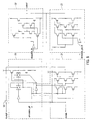
- FIG. 4 illustrates the block diagram of a bidirectional buffer 11, delimited by a discontinuous closed line, of a connection according to the invention, to achieve bidirectional CMOS links suitable for both transmission and reception.
- the transmitter stage 7 of the bidirectional buffer 11 is a three-state amplifier receiving the data to be transmitted dingd and the command signal emission_gd.
- Controlled resistors R A and R B are mounted at the interface between the transmission line and the bidirectional buffer 11.
- the controllable resistors R A and R B must theoretically be 2Z C respectively and be validated in phase opposition with the validation control signal from the three-state transmitter. This validation is obtained by the control signal emission_gd acting respectively on the inverters 12 and 13 of the controlled resistors R A and R B. The setting in phase opposition is symbolized by an inverter 14 and coupled to the output of the bidirectional buffer 11.
- FIG. 5 illustrates a first embodiment of a bidirectional transmitter of a link according to the invention, using MOSNP and MOSN transistors, respectively M A and M B , intended to behave like the resistors R A and R B of the block diagram of Figure 4.
- the MOS "resistors" R A and R B are entirely distinct from the MOS transistors of the three-state amplifier 7.
- the transistor M B is controlled, via a first switching stage 13 delimited by a discontinuous closed line, by the control signal emission_gd validating either the transmission mode or the reception mode and the transistor M A is controlled, via a second switching stage 12 delimited by a discontinuous closed line, by the same inverted control signal.
- the controlled switch 12 of FIG. 4 is produced by MOSP 12 1 and MOSN 12 2 transistors and the controlled switch 13 by MOSP 13 1 and MOSN 13 2 transistors.
- the gates of the transistors 12 1 and 12 2 receive the emission_gd control signal inverted by the inverter 14, and the gates of the transistors 13 1 and 13 2 directly receive this same signal.
- FIG. 5a schematically illustrates the behavior of the transistors 12 1 , 12 2 , 13 1 and 13 2 in switching mode in the case where the control signal emission_gd is worth a logic "1", that is to say when we are in transmission mode.
- the transistors 12 1 and 13 2 behave like closed switches, and the transistors 12 2 and 13 1 behave like open switches.
- the gate of transistor Ma then receives a logic "1" and the gate of transistor M B a logic "0" which amounts to disconnecting the "resistors" M A and M B from the transmission line AB.
- the first switching stage 13 delimited by a discontinuous closed line, behaves like two complementary switches 13 1 and 13 2 , in series with one another and with the low supply potential V SS and the output of the three-state amplifier 7 .
- the common point of the two switches 13 1 and 13 2 is coupled to the gate G B of the transistor M B , and connects the gate G B either to the low supply potential V SS in transmission, the transistor M B then being off, either at point A (drain of transistor M B ), transistor M B behaving like a resistor R B.
- the second switching stage 12 delimited by a discontinuous closed line, behaves like two complementary switches 12 1 and 12 2 , in series with one another and with the high supply potential Vdd and the output of the three-state amplifier 7.
- the common point of the two switches 12 1 and 12 2 is coupled to the gate G A of the transistor M A , and connects the gate G A either to the high supply potential V DD in transmission, the transistor M A then being off, either at point A (drain of transistor M A ), transistor M A behaving like a resistor RA.
- the equivalent scheme of the bidirectional buffer in transmission is thus reduced to diagram of FIG. 5b, and comprises the send buffer 7 which is active and the buffer reception 10 which is in this case a three-state amplifier controlled to be in the high impedance state; the output of the send buffer 7 and the input of the reception buffer 10 being respectively connected to the end A of the AB transmission line not shown.
- FIG. 5c illustrates the behavior of these same transistors when the signal of command emission_gd is worth a logical "0", that is to say when one is in reception mode.
- the transistors 12 1 and 13 2 behave like open switches, and the transistors 12 2 and 13 1 behave like closed switches.
- the gates G A and G B of the transistors M A and M B are then directly connected to the transmission line AB, not shown, and the transistors M A and M B then behave as resistors of respective value 2Z C and thus constitute the matching resistors on the AB transmission line.
- the control signal of the three-state amplifier 7 being at the logic level "0" on reception, the three-state transmitter is in the high impedance state and no longer intervenes in the equivalent scheme of the bidirectional buffer according to the invention, in reception.
- the diagram of FIG. 5c thus reduces to the diagram of FIG. 5d, and includes the reception buffer 14 which is active and the adaptation resistors corresponding respectively to the transistors M A and M B , connected to point A of the transmission line AB.
- FIG. 6 illustrates a second embodiment of a bidirectional buffer, in which the same transistors M A and M B are used both for transmission and as adaptation resistors in reception.
- CMOS switching stages 15 two CMOS switching stages 15 are used. and 16, the equivalent diagram of which is illustrated in FIG. 10.
- the switching stages 15 and 16 respectively comprise a transistor MOSN 17 and a MOSP transistor 18 connected in parallel as illustrated in the figure 10.
- the gates of transistors 17 and 18 receiving the signal respectively and the additional control signal, and the terminals input-output of the data corresponding respectively to the points common gd and dg of the two transistors 17 and 18.
- the transmitter stage comprises an amplifier 19 receiving the data to be transmitted datain, a first switching stage 15 coupled in series, at the output of amplifier 19 and controlled by the control signal emission_gd, and a second switching stage 16 coupled in series, at the output of the first stage switch 15, controlled by the same inverted control signal.
- the transistors M A and M B are mounted at the output of the switching stages 15 and 16 and at the input of the receiver stage 10, the gates G A and G B of the transistors M A and M B being common and coupled on the one hand at the output of amplifier 19 via the first switching stage 15, and on the other hand coupled to the drains D A, B of the transistors M A and M B via the second switching stage 16.
- the first and second switching stages 15 and 16 behave like complementary switches which, in transmission, connect the gates G A and Gb to the output of the amplifier 19 and disconnect the gates from the drains.
- the transistors M A and M B then behave like a CMOS amplifier.
- the switches 15 and 16 on reception, connect the drains to the gates and disconnect the gates from the output of the amplifier 19.
- the transistors then behave like resistors R A and R B.
- the assembly comprising the amplifier 19, the switching stages 15 and 16, the inverter 14 and the transistors M A and M B , defines a transmitter stage 20 of a link according to the invention.
- This transmitter stage 20 is delimited by a discontinuous closed line.
- the MOSN transistor of the first switch 15 receives a "1" logic on its gate and the MOSP transistor of the second switch 16 receives a logic "1" on its gate, and almost simultaneously, the MOSP transistor of the first switch 15 receives a logic "0" on its gate and the MOSN transistor of the second switch 16 receives a logic "0" on its grid.
- the diagram in FIG. 6b illustrates the equivalent diagram obtained in transmission, that is to say when the first switch 15 is closed and the second switch 16 is open.
- the transistors M A and M B are mounted as a transmitter in series with the transmitter buffer 19 receiving the datain data.
- the MOSN transistor of the first switch 15 receives a logic "0" on its gate and the MOSP transistor of the second switch 16 receives a logic "0" on its gate, and almost simultaneously, the MOSP transistor of the first switch 15 receives a logic "1" on its gate and the MOSN transistor of the second switch 16 receives a logic "1" on its grid.
- the diagram in FIG. 6d illustrates the equivalent diagram obtained on reception, that is to say when the first switch 15 is open and the second switch 16 is closed.
- the transistors M A and M B behave in adaptation resistors R A and R B on the end of the transmission line receiving the doutdg data, at the input of the reception buffer 10.
- the polarization conditions are different depending on the logic state "1" or "0" of the inputs / outputs, on transmission and on reception.
- the bias voltages of the gates G A and G B of the transistors M A and M B are equal to V DD or V SS .
- the polarization of the gates of the transistors is equal to 3V DD / 4 or V DD / 4.
- the resistance value will therefore be a little higher for reception than for the show
- the transistors M A and M B which are used as adaptation resistors and also participate in the emission of the datain signal, which makes it possible to use fewer transistors compared to the first embodiment, illustrated in Figure 5, and to choose as transmitter buffer 19 "small" size transistors.
- This embodiment therefore provides an additional advantage in terms of space compared to the first embodiment for which the three-state transmitter buffer 7 participated alone in the transmission proper and where the transistors M A and M B intervened only in mode reception.
- FIG. 7 illustrates a first variant of the bidirectional buffer of a link according to the invention and in which its equivalent resistance to emission can be made weaker regardless of its resistance equivalent to the reception.
- the bidirectional buffer includes a first main transmitter stage 20 corresponding to the transmitter stage, illustrated in Figure 6, and a second stage 21 corresponding to the three-state transmitter illustrated in Figure 3b. These two stages 20 and 21 are delimited respectively by a discontinuous closed line.
- the second stage 21 is mounted in parallel on the first stage 20 between the input receiving the datain data, and the output delivering the dataout data.
- inverter 14 In common and receive on their respective inputs the command signal emission_gd and the data to be transmitted datain.
- the transistors M A and M B conduct simultaneously and their equivalent resistances are found in parallel.
- the size of the transistor Ma being smaller than the transistor M A , its equivalent resistance is therefore higher than that of the transistor M A so as to provide the correction of 10 to 20% mentioned previously.
- the paralleling has the effect of lowering the value of the overall equivalent resistance.
- FIG. 8 illustrates a second variant of a bidirectional buffer of a link according to the invention, allowing additional adjustment, independent of reception and transmission to correct, for example, dispersions too high technological.
- a third stage 22 and a fourth stage 23 are added to stages 20 and 21 of the first variant.
- the stages 20, 21, 22, and 23 are demarcated respectively by a discontinuous closed line.
- the third stage 22 is a receiver stage coupled at the output of stage 20, controlled on its input by a reception control signal reception_bi, and comprising MOS transistors arranged and dimensioned to provide additional conductance in reception regardless of the show. Its output is coupled to the output common to the other three floors 20, 21 and 22 relating to the broadcast.
- Two other switches which in the transmit mode are in the blocking state, set the gates of the output transistors MOSN and MOSP respectively to V SS and V DD , which has the effect of putting them in high impedance mode.
- the fourth stage 23, corresponding to a third transmitting stage, is mounted in parallel on the first and second stages 20 and 21. It receives on a first entry the datain data and on a second entry a second control signal emission_gd_bi and includes transistors MOS arranged and sized to fine-tune the resistance setting equivalent to the broadcast.
- the electrical diagram of module 23 corresponds to that of the three-state transistor of FIG. 3b.
- stage 22 If we only use stages 20 and 22 alone, we can create a buffer bidirectional which has the same resistance values equivalent to the emission and at reception because stage 22 provides the additional conductance which missing for reception.
- FIG. 9 illustrates a third variant of a bidirectional buffer of a link according to the invention.
- floors 23 and 24 of similar architecture receive respectively a control signal emission_bi [2] and emission_bi [1], distinct from the control signal emission_gd of the first stage 20.
- the stages 20, 22, 23, and 24 are delimited respectively by a line discontinuous closed.
- the second transmitter stage 23 and the third transmitter stage 24 are mounted respectively in parallel on the first transmitter stage 20, and receive respectively on their first entries, the datain data to be sent and respectively on their second inputs the second signal emission_gd_bi [2] and the third emission control signal emission_gd_bi [1].
- MOS transistors arranged and dimensioned for fine-tuning the equivalent emission resistance independently of the reception.
- founders Manufacturers of integrated circuits, or chips, also called founders, guarantee characteristics falling within a so-called good range operation limited by an upper limit and a lower limit.
- the upper limit corresponds to the highest flow currents and therefore to the fastest chips. These chips are then stored in a class technology called BC, Anglo-Saxon abbreviations for "Best Case".
- the lower limit corresponds to the lowest flow currents and therefore to slower chips. These chips are then stored in a class technology called WC, Anglo-Saxon abbreviations for "Worst Case”.
- the amplitude of the transmitted signals is equal to V DD / 2. It is the lowest amplitude of the four cases but the two reflection coefficients are zero and the best protection against noise is thus obtained.
- V amplitude V DD Z VS R T + Z VS with R T ⁇ Z C and therefore V amplitude > V DD / 2.
- the reflection coefficient is then zero on the reception side.
- the reflection coefficient is then zero on the emission side.
- the combination BC transmitter / WC receiver results in a certain non-zero rate of return reflection of the signals but in this case the amplitude of the signals is the greatest of all the combinations (> V DD / 2 ) and is therefore most likely to support a certain rate of reflection.
- This unit corresponds to a physical reality linked to engraving technology and actually corresponds to a minimum dimension that can be engraved on the silicon.
- Lambda 0.25 ⁇ m.
- control signal emission_gd V DD
- Figures 11 to 14 give respectively in the form of voltage curves in as a function of propagation time, the results of simulations carried out at from the previous dimensioning for the emission of a pulse train in a real case, i.e. taking into account the imperfections of the line of transmission.
- the signal received at the input of the receiver after transmission on the line is shown in solid lines and the transmitter output signal in dotted.
- the signal at the input of the transmitter is not shown.
- FIG. 11 illustrates the case a) where the transmitter is WC and the receiver BC.
- Figure 12 illustrates case b) where the transmitter is BC and the receiver BC.
- Figure 13 illustrates case c) where the transmitter is WC and the receiver WC.
- FIG. 14 illustrates case d) where the transmitter is BC and the receiver WC.
- FIG. 15 illustrates the diagram, in transmission and in reception, of the current I as a function of the voltage V of the MOSN and MOSP transistors arranged in adaptation resistors, the diagram of which is shown in FIG. 16.
- This diagram illustrates by graphic resolution the dimensioning of MOSN and MOSP transistors.
- MOSN and MOSP are shown in full lines in reception mode and dashed line the characteristics of MOSN and MOSP in transmission mode.
- the resistors R A and R B must have the respective theoretical value 2ZC.
- the MOSN and MOSP transistors are dimensioned and paired so that the algebraic sum of their characteristics in reception coincides with the line ⁇ and so that their characteristics in emission intersect the line ⁇ respectively at the points of intersection E1 and E2, called rest points, for which the MOSN and MOSP respectively discharge the same current and have the same applied voltage, V DD / 4 for E2 and 3V DD / 4 for E1 in the figure.
- the receiving characteristic of the MOSN transistor tangents the abscissa axis at point V TN which corresponds to the threshold voltage of the MOSN transistor, and the receiving characteristic of the MOSN transistor tangents the abscissa axis at point V DD - V TP which corresponds to the threshold voltage of the MOSP transistor.
- the dimensioning of the MOSN and MOSP transistors therefore amounts to position the rest points on the right ⁇ according to the level of supply voltages.
- each resistor R A and R B describe curves of a parabolic nature and not a linear one, is rather an advantage in the sense that they allow adjustments of the rest points E1 and E2 by sizing practically independent of the sizes of the receiving MOSN and MOSP transistors.
- the adaptation is perfect when the line ⁇ joining E1 and E2 has a slope ⁇ V / ⁇ I equal to Z C.
Abstract
Description
La présente invention concerne les transmissions de données numériques échangées entre des circuits intégrés en utilisant des liaisons CMOS bidirectionnelles bipoints adaptées en émission et en réception.The present invention relates to digital data transmissions exchanged between integrated circuits using CMOS links bidirectional two-point adapted for transmission and reception.
L'augmentation des débits de données échangées entre un plus grand nombre de processeurs nécessite des liaisons adaptées pour transmettre ces données d'un bout à l'autre de la liaison tout en garantissant leur intégrité.The increase in data rates exchanged between a larger number of processors requires adapted links to transmit this data from one end of the link to the other while ensuring their integrity.
En effet pour des débits élevés, c'est-à-dire des fréquences élevées, il faut tenir compte de l'inductance et de la capacitance du support de transmission, dont les effets font que les variations de potentiels se propagent sous forme d'ondes progressives le long du support.Indeed for high bit rates, that is to say high frequencies, it is necessary take into account the inductance and the capacitance of the transmission medium, whose effects cause variations in potentials to propagate in the form traveling waves along the support.
La vitesse de propagation de cette onde sur la ligne est fonction de l'inductance et de la capacitance de la ligne qui définissent alors l'impédance caractéristique de la ligne.The speed of propagation of this wave on the line is a function of inductance and capacitance of the line which then define the impedance characteristic of the line.
Toute variation d'impédance ou désadaptation provoque une variation de la vitesse de propagation de l'onde qui se décompose alors en une onde transmise et une onde réfléchie qui peuvent interférer et conduire à une perte partielle ou totale des informations échangées sur la ligne.Any variation in impedance or mismatching causes a variation in the speed of propagation of the wave which then breaks down into a wave transmitted and a reflected wave that can interfere and lead to loss partial or total of the information exchanged on the line.
Pour éviter ce phénomène, on fait en sorte que la ligne possède une structure et donc une impédance caractéristique constante sur toute sa longueur.To avoid this phenomenon, we make sure that the line has a structure and therefore a constant characteristic impedance over its entire length.
Cependant il est difficile d'éviter les phénomènes de désadaptation liés notamment aux différents branchements sur la ligne, en particulier les connexions des processeurs sur la ligne. However, it is difficult to avoid the phenomena of mismatching linked in particular to the various connections on the line, in particular the processor connections on the line.
De façon générale, une transmission bidirectionnelle nécessite au niveau de chaque processeur la présence d'un étage tampon à la fois émetteur et récepteur, appelé également "buffer" bidirectionnel, couplé à la ligne de transmission par une impédance d'adaptation.In general, a two-way transmission requires at the level of each processor the presence of a buffer stage both transmitter and receiver, also called bidirectional "buffer", coupled to the line of transmission by an adaptation impedance.
La ligne de transmission tout en étant adaptée peut conserver certaines imperfections.The transmission line while being adapted can keep certain imperfections.
Le sens de transmission doit pouvoir être bidirectionnel, c'est-à-dire que sous le contrôle d'un signal de commande déterminé, chaque extrémité de la liaison peut être tantôt réceptrice, tantôt émettrice.The direction of transmission must be bidirectional, that is to say that under control of a determined control signal, each end of the link can be sometimes receiving, sometimes sending.
On peut choisir de faire des transmissions bidirectionnelles simultanément dans les deux sens ou non , mais l'option de transmission simultanée nécessite des buffers de conception extrêmement délicate capables de séparer les données émises des données reçues.You can choose to make bidirectional transmissions simultaneously in either direction or not, but the simultaneous transmission option requires extremely delicate buffers capable of separating the data sent data received.
On connaít une liaison de type GTL, abréviations anglo-saxonnes pour "Gunning Transceiver Logic" spécifiquement conçue pour réaliser des transmissions multipoints et donc capable de gérer des transmissions bipoints bidirectionnelles. Ce type de liaison est défini par le standard JEDEC et a fait l'objet d'un brevet US5023488A, intitulé "Drivers and receivers for interfacing VLSI CMOS circuits to transmission lines".We know a link type GTL, English abbreviations for "Gunning Transceiver Logic" specifically designed to perform multi-point transmissions and therefore capable of managing two-point transmissions bidirectional. This type of connection is defined by the JEDEC standard and has the subject of a patent US5023488A, entitled "Drivers and receivers for interfacing VLSI CMOS circuits to transmission lines ".
Cependant, si cette solution convient bien a des transmissions multipoints, elle est néanmoins lourde à utiliser dans le cas de liaisons bipoints. Elle a notamment pour inconvénient de ne pas utiliser toutes les capacités du GTL destiné à gérer des liaisons multipoints, tout en devant en gérer les inconvénients. However, if this solution is well suited for multipoint transmissions, it is nevertheless cumbersome to use in the case of two-point connections. She has especially for the disadvantage of not using all the capacities of the GTL intended to manage multipoint links, while having to manage them disadvantages.
Ces inconvénients sont notamment des courants et des pics de courant élevés, une alimentation spécifique, et une tension de référence à générer et à distribuer.These drawbacks are in particular high currents and current peaks, a specific supply, and a reference voltage to be generated and distribute.
On connaít également des dispositifs d'adaptation basés sur des barrettes de résistances de grande précision et de valeur ajustable, disposées en dehors des boítiers. Ces barrettes présentent un encombrement qui n'est plus négligeable sur des cartes dont les dimensions déjà limitées supportent un nombre de processeurs toujours grandissant.There are also known adaptation devices based on bars of resistors of high precision and adjustable value, arranged outside boxes. These bars have a size which is no longer negligible on maps whose already limited dimensions support a number of processors always growing.
On connaít des circuits intégrés comportant une ou plusieurs conductances réglées sur une valeur de consigne. L'intégration de conductances dans le circuit intégré permet un gain de place appréciable et réduit le problème de connexions.We know integrated circuits with one or more conductances set to a setpoint. The integration of conductances in the integrated circuit saves considerable space and reduces the problem of connections.
Un tel circuit est notamment décrit dans le brevet français n° 2 730 365 déposé par la demanderesse et intitulé "Circuit intégré avec conductance réglable à partir d'un signal numérique de commande". Ce document décrit un circuit intégré comportant au moins une conductance réglable à partir d'un signal numérique de consigne codant des échelons de valeur pour discrétiser une valeur exacte avec une précision relative fixée. La conductance est constituée de conductances élémentaires définissant chacune un échelon de valeur, tel que chaque conductance élémentaire est dimensionnée de façon à ce qu'à deux échelons de valeur successifs du signal numérique de consigne correspond un seul échelon de valeur de la conductance. S'il résulte du premier des deux échelons de valeur du signal numérique de consigne une valeur inférieure, respectivement supérieure, à la valeur exacte, conductance élémentaire correspondante est activée, respectivement désactivée. Ainsi, la valeur totale ajustée de conductance est égale à la valeur exacte avec la même précision relative, sans osciller entre deux valeurs encadrant cette valeur exacte. Such a circuit is described in particular in French patent No. 2,730,365 filed by the applicant and entitled "Integrated circuit with conductance adjustable to from a digital control signal ". This document describes a circuit integrated with at least one conductance adjustable from a signal setpoint numeric encoding value steps to discretize a exact value with fixed relative precision. Conductance is made up of elementary conductances each defining a value step, such that each elementary conductance is dimensioned so that at two successive value steps of the digital setpoint signal corresponds to only one step of value of conductance. If it results from first of the two value steps of the digital setpoint signal one value respectively higher than the exact value, conductance corresponding elementary is activated, respectively deactivated. So the adjusted total value of conductance is equal to the exact value with the same relative precision, without oscillating between two values framing this value exact.
Ce type de solution nécessite une logique complexe pour élaborer un signal de consigne permettant de commander les conductances servant à l'adaptation du circuit intégré. Cette logique de commande est de mise en oeuvre relativement lourde et augmente de façon non négligeable la taille du circuit intégré recevant ces conductances d'adaptation.This type of solution requires complex logic to develop a signal setpoint for controlling the conductances used to adapt the integrated circuit. This control logic is implemented relatively heavy and significantly increases the size of the integrated circuit receiving these adaptive conductances.
Un but de la présente invention est d'obtenir des performances équivalentes à celles obtenues sur une liaison de type GTL pour la transmission des données au premier "aller" des signaux, sans attendre un "aller-retour" sur la ligne, tout en ayant des contraintes plus faibles sur l'environnement : courants, alimentations, encapsulation (packaging).An object of the present invention is to obtain performances equivalent to those obtained on a GTL type link for data transmission at the first "go" of the signals, without waiting for a "round trip" on the line, everything by having lower constraints on the environment: currents, power supplies, encapsulation (packaging).
A cet effet, l'invention a pour premier objet une liaison CMOS bidirectionnelle bipoint du type comportant une ligne de transmission adaptée reliant respectivement à ses deux extrémités deux circuits intégrés comportant respectivement un dispositif émetteur-récepteur comportant un étage émetteur et un étage récepteur, en interface sur la ligne et commandé pour émettre ou recevoir des données numériques échangées sur la ligne de transmission en fonction d'un signal de commande pour être soit en mode émission, soit en mode réception, les dispositifs émetteur-récepteur n'étant jamais simultanément dans le même mode.To this end, the first object of the invention is a bidirectional CMOS link bipoint of the type comprising a suitable transmission line connecting respectively at its two ends two integrated circuits comprising respectively a transmitter-receiver device comprising a transmitter stage and a receiving stage, interfacing on the line and controlled to transmit or receive digital data exchanged on the transmission line in function of a control signal to be either in transmission mode or in reception mode, the transceiver devices never being simultaneously in the same mode.
Selon l'invention, la liaison est caractérisée en ce que chaque dispositif émetteur-récepteur comporte au moins un transistor MOSN et un transistor MOSP commandés respectivement par le signal de commande, dimensionnés et agencés pour adapter la liaison aux deux extrémités de la ligne de transmission. According to the invention, the connection is characterized in that each device transceiver has at least one MOSN transistor and one transistor MOSP controlled respectively by the control signal, dimensioned and arranged to adapt the connection to the two ends of the line of transmission.
Selon une caractéristique, les transistors MOSN et MOSP sont dimensionnés et agencés pour se comporter comme des résistances d'adaptation, en mode réception.According to one characteristic, the MOSN and MOSP transistors are dimensioned and arranged to behave like adaptation resistors, in reception.
Selon une autre caractéristique, les résistances d'adaptation ont des caractéristiques paraboliques et leur somme algébrique définit une caractéristique quasi linéaire dont la pente est sensiblement égale à la valeur de l'impédance caractéristique de la ligne de transmission.According to another characteristic, the adaptation resistors have parabolic characteristics and their algebraic sum defines a almost linear characteristic whose slope is substantially equal to the value characteristic impedance of the transmission line.
L'invention a notamment pour avantage d'amortir les effets dus au boítier, vu du côté récepteur, et d'utiliser les transistors des buffers, implantés sur le circuit intégré, pour réaliser l'adaptation de la liaison tout en réduisant le nombre et la taille des transistors MOS.The invention particularly has the advantage of absorbing the effects due to the housing, seen on the receiver side, and use the buffers transistors, located on the integrated circuit, to adapt the link while reducing the number and size of MOS transistors.
L'invention n'utilise pas des signaux de commande particuliers mais uniquement les signaux de validation des dispositifs émetteur-récepteur des circuits intégrés.The invention does not use particular control signals but only the validation signals from the transceiver devices of the integrated circuits.
Un autre avantage est de supprimer le besoin de résistances externes entraínant un moindre coût, et donc de faciliter le tracé de la carte imprimée.Another advantage is to eliminate the need for external resistors resulting in a lower cost, and therefore facilitate the layout of the printed map.
Cet avantage est loin d'être négligeable et peut même devenir primordial quand on envisage des centaines et même au-delà du millier de liaisons à partir d'un même boítier.This advantage is far from negligible and can even become essential when we consider hundreds and even beyond a thousand links to from the same box.
Un autre avantage de résistances d'adaptation intégrées selon l'invention, est que si la dispersion technologique est telle que les transistors MOSP et MOSN ont une dispersion d'appariement par rapport à une technologie parfaitement centrée, le sens de variation du générateur de tension de Thévenin, équivalent des résistances intégrées, varie dans le même sens que la tension de basculement de l'inverseur utilisé en détecteur d'entrée. Il y a donc au moins une compensation partielle des dispersions.Another advantage of integrated adaptation resistors according to the invention is that if the technological dispersion is such that the MOSP and MOSN transistors have a matching dispersion compared to a technology perfectly centered, the direction of variation of the Thévenin voltage generator, equivalent integrated resistors, varies in the same direction as the voltage of tilting of the inverter used as an input detector. So there is at least partial compensation for dispersions.
Enfin, l'implantation des résistances terminales RT sur le circuit intégré est ce qui donne la meilleure atténuation des oscillations parasites induites par les désadaptations du fait des connecteurs du boítier.Finally, the implantation of the terminal resistors R T on the integrated circuit is what gives the best attenuation of the parasitic oscillations induced by the mismatches due to the connectors of the case.
D'autres avantages et caractéristiques de la présente invention apparaítront à la lecture de la description qui suit faite en référence aux figures annexées qui représentent :
- la figure 1, un schéma de principe d'une liaison monodirectionnelle CMOS adaptée en émission et en réception ;
- la figure 1a, un schéma électrique d'un émetteur représenté par un inverseur sur la figure 1 ;
- la figure 1b, le schéma équivalent de l'émetteur ;
- la figure 2, un schéma de principe d'une liaison bidirectionnelle adaptée en réception en utilisant des résistances fixes ;
- la figure 2a, le schéma équivalent de l'émetteur de la liaison bidirectionnelle de la figure 2 ;
- les figures 3a et 3b, respectivement deux exemples de schémas d'émetteurs à trois états ;
- la figure 4, un schéma de principe d'un buffer bidirectionnel d'une liaison selon l'invention, avec des résistances commandées distinctes de l'émetteur ;
- la figure 5, le schéma électrique du buffer de la figure 4 ;
- la figure 5a, le schéma comportemental des étages de commutation du buffer de la figure 4 en émission ;
- la figure 5b, le schéma équivalent du buffer de la figure 4 en émission ;
- la figure 5c, le schéma comportemental des étages de commutation du buffer de la figure 4 en réception ;
- la figure 5d, le schéma équivalent du buffer de la figure 4 en réception ;
- la figure 6, un schéma électrique d'un buffer d'une liaison selon l'invention avec des résistances commandées et fusionnées avec l'émetteur ;
- la figure 6a, le schéma comportemental des étages de commutation du buffer de la figure 6, en émission ;
- la figure 6b, le schéma équivalent du buffer de la figure 6, en émission ;
- la figure 6c, le schéma comportemental des étages de commutation du buffer de la figure 6, en réception ;
- la figure 6d, le schéma équivalent du buffer de la figure 6, en réception ;
- la figure 7, un schéma de principe d'un émetteur mixte ayant une résistance à l'émission inférieure à la résistance à la réception ;
- la figure 8, un schéma de principe d'un émetteur mixte ayant une résistance à l'émission inférieure à la résistance à la réception avec un réglage d'impédance indépendant à l'émission et à la réception ;
- la figure 9, un schéma de principe d'un émetteur mixte ayant une résistance à l'émission inférieure à la résistance à la réception, avec des réglages d'impédance indépendants à l'émission et à la réception ;
- la figure 10, le schéma électrique des étages de commutation du buffer de la figure 6 ;
- la figure 11, la réponse d'un buffer selon la figure 7 configuré en émetteur WC et en récepteur BC, à un train d'impulsions dans le cas réel ;
- la figure 12, la réponse d'un buffer selon la figure 7 configuré en émetteur BC et en récepteur BC, à un train d'impulsions dans le cas réel ;
- la figure 13, la réponse d'un buffer selon la figure 7 configuré en émetteur WC et en récepteur WC, à un train d'impulsions dans le cas réel ;
- la figure 14, la réponse d'un buffer selon la figure 7 configuré en émetteur BC et en récepteur WC, à un train d'impulsions dans le cas réel ;
- la figure 1 5, le schéma électrique des transistors MOS d'adaptation montés en résistances d'adaptation ; et
- la figure 16, un diagramme de la résolution graphique du dimensionnement des transistors MOS d'adaptation.
- Figure 1, a block diagram of a CMOS one-way link suitable for transmission and reception;
- FIG. 1a, an electrical diagram of a transmitter represented by an inverter in FIG. 1;
- Figure 1b, the equivalent diagram of the transmitter;
- Figure 2, a block diagram of a bidirectional link adapted for reception using fixed resistors;
- Figure 2a, the equivalent diagram of the transmitter of the bidirectional link of Figure 2;
- FIGS. 3a and 3b, respectively two examples of diagrams of transmitters with three states;
- Figure 4, a block diagram of a bidirectional buffer of a link according to the invention, with controlled resistors distinct from the transmitter;
- Figure 5, the electrical diagram of the buffer of Figure 4;
- FIG. 5a, the behavioral diagram of the switching stages of the buffer of FIG. 4 in transmission;
- FIG. 5b, the equivalent diagram of the buffer of FIG. 4 in transmission;
- FIG. 5c, the behavioral diagram of the switching stages of the buffer of FIG. 4 on reception;
- FIG. 5d, the equivalent diagram of the buffer of FIG. 4 on reception;
- FIG. 6, an electrical diagram of a buffer of a link according to the invention with resistors controlled and merged with the transmitter;
- FIG. 6a, the behavioral diagram of the switching stages of the buffer of FIG. 6, in transmission;
- FIG. 6b, the equivalent diagram of the buffer of FIG. 6, in transmission;
- FIG. 6c, the behavioral diagram of the switching stages of the buffer of FIG. 6, on reception;
- FIG. 6d, the equivalent diagram of the buffer of FIG. 6, on reception;
- FIG. 7, a block diagram of a mixed transmitter having a resistance to transmission lower than the resistance to reception;
- FIG. 8, a block diagram of a mixed transmitter having a resistance to transmission lower than the resistance to reception with an independent impedance setting at transmission and reception;
- FIG. 9, a block diagram of a mixed transmitter having a transmission resistance lower than the reception resistance, with independent impedance settings on transmission and reception;
- Figure 10, the electrical diagram of the switching stages of the buffer of Figure 6;
- FIG. 11, the response of a buffer according to FIG. 7 configured as a WC transmitter and a BC receiver, to a train of pulses in the real case;
- FIG. 12, the response of a buffer according to FIG. 7 configured as a transmitter BC and a receiver BC, to a train of pulses in the real case;
- FIG. 13, the response of a buffer according to FIG. 7 configured as a WC transmitter and a WC receiver, to a train of pulses in the real case;
- FIG. 14, the response of a buffer according to FIG. 7 configured as a BC transmitter and a WC receiver, to a train of pulses in the real case;
- Figure 1 5, the electrical diagram of the MOS adaptation transistors mounted in adaptation resistors; and
- FIG. 16, a diagram of the graphic resolution of the dimensioning of the adaptation MOS transistors.
Sur ces figures, les mêmes éléments sont désignés par le même repère.In these figures, the same elements are designated by the same reference.
La figure 1 illustre schématiquement un exemple de liaison CMOS monodirectionnelle en émission et en réception, adaptée à ses deux extrémités.Figure 1 schematically illustrates an example of CMOS link unidirectional in transmission and reception, suitable for both extremities.
On a représenté une ligne de transmission AB de longueur déterminée et
d'impédance caractéristique ZC reliant un émetteur 1 connecté à son entré A, à
un récepteur 2 connecté à sa sortie B. L'émetteur 1 et le récepteur 2 sont
représentés respectivement par un inverseur. Un pont 3 de deux résistances,
respectivement de valeur R = 2ZC, est connecté en B. Le pont 3 est alimenté
entre une tension d'alimentation haute VDD et une tension d'alimentation basse
VSS.There is shown a transmission line AB of determined length and characteristic impedance Z C connecting a
Vu du côté récepteur 2, le pont de résistances 3 présente un schéma de
Thévenin équivalent d'impédance ZC en série avec un générateur de tension
de valeur égale à VDD/2.Seen from the
La figure 1a illustre le schéma électrique de l'émetteur 1, réalisé à partir d'un
CMOS constitué d'un transistor MOSN 4 et d'un transistor MOSP 5 montés de
manière connue.FIG. 1a illustrates the electrical diagram of the
La figure 1b illustre le schéma équivalent de l'émetteur 1 se comportant comme
un inverseur 6 commandé par un signal de commande din et délivrant un
signal de sortie dout.FIG. 1b illustrates the equivalent diagram of the
Si le dimensionnement des transistors est correct, c'est-à-dire si les
résistances équivalentes des transistors MOSN 4 et MOSP 5 sont de valeur
identique, le schéma équivalent peut se réduire à une résistance RT = ZC
commutée entre VDD et VSS, RT sera appelée par la suite, résistance terminale
du schéma équivalent de Thévenin de l'émetteur ou du récepteur. If the sizing of the transistors is correct, that is to say if the equivalent resistances of the
Dans ces conditions, l'amplitude des signaux transmis est égale à VDD/2 centré sur VDD/2, ce qui signifie que le niveau bas transmis est égal à VDD/4 et le niveau haut à 3VDD/4.Under these conditions, the amplitude of the transmitted signals is equal to V DD / 2 centered on V DD / 2, which means that the low level transmitted is equal to V DD / 4 and the high level to 3V DD / 4.
Le coefficient de réflexion à une extrémité quelconque de la ligne est égale à :
Creflex est compris entre -1 (quand la ligne est branchée sur un court-circuit ou
sur un générateur de tension pur, dans ce cas RT = 0) et +1 (quand l'extrémité
de la ligne est en l'air ou branchée sur un générateur de courant).
L'intérêt de l'adaptation aux deux extrémités est que si l'adaptation n'est pas
parfaite, la résistance terminale s'exprime par :
Par exemple, si la résistance terminale RT est à +/- 20% de la valeur Zc à chaque extrémité de la ligne, la première réflexion a une amplitude de 10% du premier signal transmis, la seconde réflexion du coté récepteur aura une amplitude de 1% du premier signal.For example, if the terminal resistance R T is +/- 20% of the value Z c at each end of the line, the first reflection has an amplitude of 10% of the first transmitted signal, the second reflection on the receiver side will have a amplitude of 1% of the first signal.
La seconde réflexion se mélange avec le nouveau signal émis, car on n'attend pas qu'un signal soit arrivé pour émettre le suivant. Il est donc important que l'atténuation des réflexions après un "aller-retour-aller" soit forte pour éviter des intermodulations de signaux. Ces réflexions multiples sont vues comme un bruit pour les signaux transmis au premier "aller". The second reflection mixes with the new signal emitted, because we do not wait not that a signal has arrived to send the next one. It is therefore important that the attenuation of reflections after a "round trip-round trip" is strong to avoid signal intermodulations. These multiple reflections are seen as a noise for signals transmitted on the first "go".
On constate donc que la double adaptation même non parfaite conduit à de fortes atténuations des réflexions et garantit donc une bonne intégrité des signaux transmis.It can therefore be seen that the double adaptation, even if not perfect, leads to strong attenuation of reflections and therefore guarantees good integrity of transmitted signals.
Un autre effet de l'adaptation en réception est l'atténuation et l'amortissement des signaux parasites oscillatoires induits par des désadaptations locales telles que les traversées des connecteurs intermédiaires et des connecteurs du boítier des circuits intégrés.Another effect of reception adaptation is attenuation and damping oscillatory parasitic signals induced by local mismatches such that the bushings of the intermediate connectors and the connectors of the case of integrated circuits.
Quand on ne peut pas assurer une adaptation exacte, il vaut mieux en réception avoir RT > ZC avec un coefficient Creflex > 0 , ce qui augmente l'amplitude du signal reçu, et en émission RT < ZC, ce qui augmente également l'amplitude du signal émis.When one cannot ensure an exact adaptation, it is better in reception to have R T > Z C with a Creflex coefficient> 0, which increases the amplitude of the received signal, and in emission R T <Z C , which increases also the amplitude of the signal transmitted.
Le bruit généré par les réflexions multiples sera en effet d'autant plus "tolérable" que les niveaux transmis sont élevés.The noise generated by the multiple reflections will indeed be all the more "tolerable" that the transmitted levels are high.
On désignera par le critère CNOP, abréviations de "Critère de Non Optimisation Préférable", cette tolérance de désadaptation.We will designate by the CNOP criterion, abbreviations of "No Criterion Preferable Optimization ", this mismatch tolerance.
Le schéma de la figure 2 illustre la liaison précédente modifiée pour réaliser une liaison bidirectionnelle, avec des résistances fixes pour conserver l'adaptation en réception.The diagram in Figure 2 illustrates the previous link modified to achieve a bidirectional link, with fixed resistors to keep adaptation in reception.
Les extrémités de la ligne AB sont couplées respectivement au point milieu
d'un pont de résistances 3 similaire à celui de la figure 1.The ends of the line AB are coupled respectively to the midpoint
a
L'émetteur utilisé pour une liaison bidirectionnelle est un amplificateur 7
"tristates", ou trois états, dont le schéma équivalent est illustré à la figure 2a
dans son état actif, c'est-à-dire quand le premier inverseur 8 commandé est
branché sur VDD (ou VSS). The transmitter used for a bidirectional link is an
Pour conserver une même amplitude des signaux autour de VDD/2, il faut que
l'amplificateur 7 présente une résistance équivalente Re = ZC /2.To keep the same amplitude of the signals around V DD / 2, the
On a représenté un deuxième interrupteur 9 en série avec la résistance
équivalente Re. Ce deuxième interrupteur 9 est commandé par un signal de
validation qui à l'état logique "1" commande l'émission et qui à l'état logique "0"
met l'émetteur dans l'état haute impédance ; l'amplificateur 7 est désactivé et
peut être alors considéré comme un circuit ouvert au point A.A
Pour la réception, un récepteur ou un buffer de réception 10, également
représenté comme un inverseur, est couplé au point A et délivre le signal
doutdg véhiculé par la ligne de transmission AB. L'amplificateur trois états 7 et
le récepteur 10 constituent un étage émetteur-récepteur bidirectionnel appelé
également buffer bidirectionnel 11 et délimité par une ligne fermée discontinue.For reception, a receiver or a
On a représenté de manière symétrique au point B, un buffer bidirectionnel 11' identique au buffer 11.We have represented symmetrically at point B, a bidirectional buffer 11 ' identical to buffer 11.
Du fait de cette symétrie, on ne représentera dans les figures qui suivent, et donc on ne décrira dans la suite de la description, que le buffer bidirectionnel disposé à gauche de la ligne de transmission AB.Because of this symmetry, we will not represent in the following figures, and so we will only describe in the following description, the bidirectional buffer located to the left of the AB transmission line.
Les figures 3a et 3b illustrent respectivement deux schémas d'amplificateur trois états parmi d'autres schémas possibles. Un amplificateur trois états est nécessaire dans le cas d'une transmission bidirectionnelle telle que celle illustrée à la figure 2 et permet d'inverser le sens de transmission.Figures 3a and 3b respectively illustrate two amplifier diagrams three states among other possible schemes. A three-state amplifier is necessary in the case of a bidirectional transmission such as that illustrated in Figure 2 and allows to reverse the direction of transmission.
L'amplificateur de la figure 3b utilise moins de transistors que celui de la figure 3a (6 au lieu de 8) tout en conservant des caractéristiques électriques similaires. The amplifier of figure 3b uses fewer transistors than that of figure 3a (6 instead of 8) while retaining electrical characteristics similar.
Une première conséquence néfaste liée à la configuration de la figure 2 est une consommation en courant doublée, toutes les impédances étant divisées par deux.A first harmful consequence related to the configuration of FIG. 2 is double current consumption, all impedances divided by two.
Une deuxième conséquence néfaste est que, étant donné que du côté émetteur la liaison n'est plus adaptée, en effet on a ZC/2 en parallèle avec ZC soit ZC/3, le coefficient de réflexion ne vaut plus théoriquement 0 même si la ligne est parfaitement adaptée, mais vaut (ZC/3 - ZC) / (ZC/3 + ZC) soit - 1/2, si bien que la liaison est moins bien protégée contre les réflexions multiples, en cas d'adaptation approximative de la ligne.A second harmful consequence is that, given that on the transmitter side the link is no longer suitable, in fact we have Z C / 2 in parallel with Z C, ie Z C / 3, the reflection coefficient is no longer theoretically equal to 0 if the line is perfectly adapted, but is equal to (Z C / 3 - Z C ) / (Z C / 3 + Z C ) or - 1/2, so that the connection is less well protected against multiple reflections, in case approximate line adaptation.
L'idée de l'invention consiste à intégrer des résistances d'adaptation sur le circuit intégré lui-même, sous forme de transistors MOS et aptes à être commandés par les signaux de commande validant l'émission ou la réception, de façon à contrôler la mise en oeuvre ou au contraire la mise hors-circuit des résistances d'adaptation. On cherche donc à se ramener au schéma de principe de la figure 1, et ceci quel que soit le sens de transfert des données.The idea of the invention consists in integrating adaptation resistors on the integrated circuit itself, in the form of MOS transistors and capable of being controlled by control signals validating transmission or reception, so as to control the implementation or on the contrary the deactivation of the adaptation resistances. We therefore seek to reduce ourselves to the diagram of principle of Figure 1, regardless of the direction of data transfer.
La figure 4 illustre le schéma de principe d'un buffer bidirectionnel 11, délimité
par une ligne fermée discontinue, d'une liaison selon l'invention, pour réaliser
des liaisons CMOS bidirectionnelles adaptées à la fois en émission et en
réception.FIG. 4 illustrates the block diagram of a
L'étage émetteur 7 du buffer bidirectionnel 11 est un amplificateur trois états
recevant les données à émettre dingd et le signal de commande émission_gd.The
Des résistances commandées RA et RB, délimitées respectivement par une
ligne fermée discontinue, sont montées en interface entre la ligne de
transmission et le buffer bidirectionnel 11. Controlled resistors R A and R B , delimited respectively by a discontinuous closed line, are mounted at the interface between the transmission line and the
Les résistances commandables RA et RB doivent valoir théoriquement
respectivement 2ZC et être validées en opposition de phase avec le signal de
commande de validation de l'émetteur trois états. Cette validation est obtenue
par le signal de commande émission_gd agissant respectivement sur les
inverseurs 12 et 13 des résistances commandées RA et RB. La mise en
opposition de phase est symbolisée par un inverseur 14 et couplé à la sortie du
buffer bidirectionnel 11.The controllable resistors R A and R B must theoretically be 2Z C respectively and be validated in phase opposition with the validation control signal from the three-state transmitter. This validation is obtained by the control signal emission_gd acting respectively on the
Le fonctionnement d'un buffer CMOS bidirectionnel d'une liaison selon l'invention est maintenant décrit en référence aux schémas électriques des modes de réalisation illustrés aux figures 5 et 6.The operation of a bidirectional CMOS buffer of a link according to the invention is now described with reference to the electrical diagrams of embodiments illustrated in FIGS. 5 and 6.
La figure 5 illustre un premier mode de réalisation d'un émetteur bidirectionnel d'une liaison selon l'invention, mettant en oeuvre des transistors MOSNP et MOSN, respectivement MA et MB, destinés à se comporter comme les résistances RA et RB du schéma de principe de la figure 4.FIG. 5 illustrates a first embodiment of a bidirectional transmitter of a link according to the invention, using MOSNP and MOSN transistors, respectively M A and M B , intended to behave like the resistors R A and R B of the block diagram of Figure 4.
Dans ce mode de réalisation, les "résistances" MOS RA et RB sont tout à fait
distinctes des transistors MOS de l'amplificateur trois états 7.In this embodiment, the MOS "resistors" R A and R B are entirely distinct from the MOS transistors of the three-
Le transistor MB est commandé, via un premier étage de commutation 13
délimité par une ligne fermée discontinue, par le signal de commande
émission_gd validant soit le mode émission soit le mode réception et le
transistor MA est commandé, via un deuxième étage de commutation 12
délimité par une ligne fermée discontinue, par le même signal de commande
inversé.The transistor M B is controlled, via a
L'interrupteur commandé 12 de la figure 4 est réalisé par des transistors MOSP
121 et MOSN 122 et l'interrupteur commandé 13 par les transistors MOSP 131
et MOSN 132. Les grilles des transistors 121 et 122 reçoivent le signal de
commande émission_gd inversé par l'inverseur 14, et les grilles des transistors
131 et 132 reçoivent directement ce même signal.The controlled
La figure 5a illustre de façon schématique le comportement des transistors 121,
122, 131 et 132 en régime de commutation dans le cas où le signal de
commande émission_gd vaut un "1" logique, c'est-à-dire quand on est dans le
mode émission.FIG. 5a schematically illustrates the behavior of the
Dans le mode émission, les transistors 121 et 132 se comportent comme des
interrupteurs fermés, et les transistors 122 et 131 se comportent comme des
interrupteurs ouverts. La grille du transistor Ma reçoit alors un "1" logique et la
grille du transistor MB un "0" logique ce qui revient à déconnecter les
"résistances" MA et MB de la ligne de transmission AB.In the transmission mode, the
Le premier étage de commutation 13, délimité par une ligne fermée
discontinue, se comporte comme deux interrupteurs complémentaires 131 et
132, en série entre eux et avec le potentiel d'alimentation basse VSS et la sortie
de l'amplificateur trois états 7.The
Le point commun des deux interrupteurs 131 et 132 est couplé à la grille GB du
transistor MB, et connecte la grille GB soit au potentiel d'alimentation basse
VSS en émission, le transistor MB étant alors hors circuit, soit au point A (drain
du transistor MB), le transistor MB se comportant comme une résistance RB.The common point of the two
Le deuxième étage de commutation 12, délimité par une ligne fermée
discontinue, se comporte comme deux interrupteurs complémentaires 121 et
122, en série entre eux et avec le potentiel d'alimentation haute Vdd et la sortie
le l'amplificateur trois états 7.The
Le point commun des deux interrupteurs 121 et 122 est couplé à la grille GA du
transistor MA, et connecte la grille GA soit au potentiel d'alimentation haute
VDD en émission, le transistor MA étant alors hors circuit, soit au point A (drain
du transistor MA), le transistor MA se comportant comme une résistance RA.The common point of the two
Le schéma équivalent du buffer bidirectionnel en émission se réduit ainsi au
schéma de la figure 5b, et comporte le buffer émission 7 qui est actif et le
buffer réception 10 qui est dans ce cas un amplificateur trois états commandé
pour être dans l'état haute impédance ; la sortie du buffer émission 7 et l'entrée
du buffer réception 10 étant respectivement connectées à l'extrémité A de la
ligne de transmission AB non représentée.The equivalent scheme of the bidirectional buffer in transmission is thus reduced to
diagram of FIG. 5b, and comprises the
La figure 5c illustre le comportement de ces mêmes transistors quand le signal de commande émission_gd vaut un "0" logique, c'est-à-dire quand on est dans le mode réception.FIG. 5c illustrates the behavior of these same transistors when the signal of command emission_gd is worth a logical "0", that is to say when one is in reception mode.
Dans le mode réception, les transistors 121 et 132 se comportent comme des
interrupteurs ouverts, et les transistors 122 et 131 se comportent comme des
interrupteurs fermés. Les grilles GA et GB des transistors MA et MB sont alors
directement branchées à la ligne de transmission AB, non représentée, et les
transistors MA et MB se comportent alors comme des résistances de valeur
respective 2ZC et constituent ainsi les résistances d'adaptation sur la ligne de
transmission AB.In the reception mode, the
Le signal de commande de l'amplificateur trois états 7 étant au niveau logique
"0" en réception, l'émetteur trois états est dans l'état haute impédance et
n'intervient donc plus dans le schéma équivalent du buffer bidirectionnel selon
l'invention, en réception.The control signal of the three-
Le schéma de la figure 5c se réduit ainsi au schéma de la figure 5d, et
comporte le buffer réception 14 qui est actif et les résistances d'adaptation
correspondant respectivement aux transistors MA et MB, connectés au point A
de la ligne de transmission AB. The diagram of FIG. 5c thus reduces to the diagram of FIG. 5d, and includes the
La figure 6 illustre un deuxième mode de réalisation d'un buffer bidirectionnel, dans lequel les mêmes transistors MA et MB sont utilisés à la fois pour l'émission et comme résistances d'adaptation en réception.FIG. 6 illustrates a second embodiment of a bidirectional buffer, in which the same transistors M A and M B are used both for transmission and as adaptation resistors in reception.
Dans ce mode de réalisation, on utilise deux étages de commutation CMOS 15 et 16 dont le schéma équivalent est illustré à la figure 10.In this embodiment, two CMOS switching stages 15 are used. and 16, the equivalent diagram of which is illustrated in FIG. 10.
Les étages de commutation 15 et 16, comportent respectivement un transistor
MOSN 17 et un transistor MOSP 18 montés en parallèle comme illustré à la
figure 10. Les grilles des transistors 17 et 18 recevant respectivement le signal
de commande et le signal de commande complémentaire, et les bornes
d'entrée-sortie des données correspondant respectivement aux points
communs gd et dg des deux transistors 17 et 18.The switching stages 15 and 16, respectively comprise a
Si une tension positive est appliquée sur la borne gd et une tension négative
est appliquée sur la borne dg de l'étage de commutation 15 ou 16, alors la
source du transistor 17 sera du côté de la borne dg.If a positive voltage is applied to the gd terminal and a negative voltage
is applied to terminal dg of switching
Un tel montage permet d'optimiser la conduction ou la non conduction du
MOSN 17 et du MOSP 18 dans les deux sens de passage du courant à travers
l'interrupteur 15 ou 16. On réalise ainsi un interrupteur presque parfait. Il faut
également que les signaux de commande arrivant respectivement sur les
grilles des MOSN 17 et du MOSP 18 soient en opposition de phase.Such an arrangement makes it possible to optimize the conduction or non-conduction of the
L'étage émetteur comporte un amplificateur 19 recevant les données à émettre
datain, un premier étage de commutation 15 couplé en série, en sortie de
l'amplificateur 19 et commandé par le signal de commande émission_gd, et un
deuxième étage de commutation 16 couplé en série, en sortie du premier étage
de commutation 15, commandé par le même signal de commande inversé. The transmitter stage comprises an
Les transistors MA et MB sont montés en sortie des étages de commutation 15
et 16 et en entrée de l'étage récepteur 10, les grilles GA et GB des transistors
MA et MB étant communes et couplées d'une part à la sortie de l'amplificateur
19 via le premier étage de commutation 15, et couplées d'autre part aux drains
DA,B des transistors MA et MB via le deuxième étage de commutation 16.The transistors M A and M B are mounted at the output of the switching stages 15 and 16 and at the input of the
Le premier et le deuxième étages de commutation 15 et 16 se comportent
comme des interrupteurs complémentaires qui, en émission, connectent les
grilles GA et Gb à la sortie de l'amplificateur 19 et déconnectent les grilles des
drains. Les transistors MA et MB se comportent alors comme un amplificateur
CMOS.The first and second switching stages 15 and 16 behave like complementary switches which, in transmission, connect the gates G A and Gb to the output of the
Les interrupteurs 15 et 16, en réception, connectent les drains aux grilles et
déconnectent les grilles de la sortie de l'amplificateur 19. Les transistors se
comportent alors comme des résistances RA et RB.The
L'ensemble comportant l'amplificateur 19, les étages de commutation 15 et 16,
l'inverseur 14 et les transistors MA et MB, définit un étage émetteur 20 d'une
liaison selon l'invention. Cet étage émetteur 20 est délimité par une ligne
fermée discontinue.The assembly comprising the
La figure 6a illustre de façon schématique le comportement des interrupteurs
CMOS 15 et 16 dans le cas où le signal de commande émission_gd = "1"
logique, c'est-à-dire quand on est dans le mode émission.FIG. 6a schematically illustrates the behavior of the
A l'émission, le transistor MOSN du premier interrupteur 15 reçoit un "1"
logique sur sa grille et le transistor MOSP du deuxième interrupteur 16 reçoit
un "1" logique sur sa grille, et quasi simultanément, le transistor MOSP du
premier interrupteur 15 reçoit un "0" logique sur sa grille et le transistor MOSN
du deuxième interrupteur 16 reçoit un "0" logique sur sa grille. On transmission, the MOSN transistor of the
Le schéma de la figure 6b illustre le schéma équivalent obtenu en émission,
c'est-à-dire quand le premier interrupteur 15 est fermé et le deuxième
interrupteur 16 est ouvert. Les transistors MA et MB sont montés en émetteur
en série avec le buffer émetteur 19 recevant les données datain.The diagram in FIG. 6b illustrates the equivalent diagram obtained in transmission, that is to say when the
La figure 6c illustre de façon schématique le comportement des interrupteurs
CMOS 15 et 16 dans le cas où le signal de commande émission_gd = "0"
logique, c'est-à-dire quand on est dans le mode réception.FIG. 6c schematically illustrates the behavior of the
Le transistor MOSN du premier interrupteur 15 reçoit un "0" logique sur sa
grille et le transistor MOSP du deuxième interrupteur 16 reçoit un "0" logique
sur sa grille, et quasi simultanément, le transistor MOSP du premier
interrupteur 15 reçoit un "1" logique sur sa grille et le transistor MOSN du
deuxième interrupteur 16 reçoit un "1" logique sur sa grille.The MOSN transistor of the
Le schéma de la figure 6d illustre le schéma équivalent obtenu en réception,
c'est-à-dire quand le premier interrupteur 15 est ouvert et le deuxième
interrupteur 16 est fermé. Les transistors MA et MB se comportent en
résistances d'adaptation RA et RB sur l'extrémité de la ligne de transmission
recevant les données doutdg, en entrée du buffer de réception 10.The diagram in FIG. 6d illustrates the equivalent diagram obtained on reception, that is to say when the
Les conditions de polarisation sont différentes suivant l'état logique "1" ou "0" des entrées/sorties, à l'émission et à la réception. A l'émission, les tensions de polarisation des grilles GA et GB des transistors MA et MB sont égales à VDD ou VSS. A la réception, la polarisation des grilles des transistors est égale à 3VDD/4 ou VDD/4.The polarization conditions are different depending on the logic state "1" or "0" of the inputs / outputs, on transmission and on reception. On transmission, the bias voltages of the gates G A and G B of the transistors M A and M B are equal to V DD or V SS . On reception, the polarization of the gates of the transistors is equal to 3V DD / 4 or V DD / 4.
La valeur des résistances sera donc un peu plus élevée pour la réception que pour l'émission The resistance value will therefore be a little higher for reception than for the show
Il y a aussi la mise en parallèle partielle des résistances effectives des transistors MOSN et MOSP dont il faut tenir compte et qui aurait tendance à agir dans le sens contraire ; le transistor MOSN étant surtout efficace au niveau haut et le transistor MOSP au niveau bas. Cet effet étant cependant peu sensible, l'ensemble des considérations précédentes fera que le critère CNOP, dans le sens précédemment défini, sera automatiquement rempli.There is also the partial paralleling of the effective resistances of MOSN and MOSP transistors which must be taken into account and which would tend to act in the opposite direction; the MOSN transistor being especially effective at high level and the MOSP transistor low. This effect being however little sensitive, all of the above considerations will make the CNOP criterion, in the direction previously defined, will be automatically filled.
Dans ce mode de réalisation, les transistors MA et MB qui sont utilisés comme
résistances d'adaptation et participent également à l'émission du signal datain,
ce qui permet d'utiliser moins de transistors par rapport au premier mode de
réalisation, illustré à la figure 5, et de choisir comme buffer émetteur 19 des
transistors "petits" en dimension. Ce mode de réalisation apporte donc un
avantage supplémentaire en terme de place par rapport au premier mode de
réalisation pour lequel le buffer émetteur trois états 7, participait seul à
l'émission proprement dite et où les transistors MA et MB intervenaient
uniquement en mode réception.In this embodiment, the transistors M A and M B which are used as adaptation resistors and also participate in the emission of the datain signal, which makes it possible to use fewer transistors compared to the first embodiment, illustrated in Figure 5, and to choose as
La figure 7 illustre une première variante du buffer bidirectionnel d'une liaison selon l'invention et dans laquelle sa résistance équivalente à l'émission peut être rendue plus faible indépendamment de sa résistance équivalente à la réception.FIG. 7 illustrates a first variant of the bidirectional buffer of a link according to the invention and in which its equivalent resistance to emission can be made weaker regardless of its resistance equivalent to the reception.
Dans cette première variante, le buffer bidirectionnel comporte un premier
étage émetteur principal 20 correspondant à l'étage émetteur, illustré à la
figure 6, et un deuxième étage 21 correspondant à l'émetteur trois états illustré
à la figure 3b. Ces deux étages 20 et 21 sont délimités respectivement par une
ligne fermée discontinue.In this first variant, the bidirectional buffer includes a first
Le deuxième étage 21 est monté en parallèle sur le premier étage 20 entre
l'entrée recevant les données datain, et la sortie délivrant les données dataout. The
Ils ont en commun l'inverseur 14 et reçoivent sur leurs entrées respectives le
signal de commande émission_gd et les données à transmettre datain.They have the
Dans le cas où un ajustement de 10 ou 20% de la résistance équivalente est nécessaire, seuls les transistors MA et MB sont "gros" du point de vue dimensionnel; les transistors Ma et Mb servant juste à donner un complément de conductance gardent une taille en proportion relativement modeste.In the case where an adjustment of 10 or 20% of the equivalent resistance is necessary, only the transistors M A and M B are "large" from the dimensional point of view; the Ma and Mb transistors just used to give additional conductance keep a relatively modest size.
En émission, les transistors MA et MB conduisent simultanément et leurs résistances équivalente se retrouvent en parallèle. La taille du transistor Ma étant plus réduite que le transistor MA, sa résistance équivalente est donc plus forte que celle du transistor MA de façon à apporter la correction de 10 à 20 % citée précédemment. La mise en parallèle a pour effet d'abaisser la valeur de la résistance équivalente globale.In transmission, the transistors M A and M B conduct simultaneously and their equivalent resistances are found in parallel. The size of the transistor Ma being smaller than the transistor M A , its equivalent resistance is therefore higher than that of the transistor M A so as to provide the correction of 10 to 20% mentioned previously. The paralleling has the effect of lowering the value of the overall equivalent resistance.
La figure 8 illustre une deuxième variante d'un buffer bidirectionnel d'une liaison selon l'invention, permettant un réglage supplémentaire, indépendant à la réception et à l'émission pour corriger par exemple des dispersions technologiques trop élevées.FIG. 8 illustrates a second variant of a bidirectional buffer of a link according to the invention, allowing additional adjustment, independent of reception and transmission to correct, for example, dispersions too high technological.
Un troisième étage 22 et un quatrième étage 23 sont ajoutés aux étages 20 et
21 de la première variante. Les étages 20, 21, 22, et 23 sont délimités
respectivement par une ligne fermée discontinue.A
Le troisième étage 22 est un étage récepteur couplé en sortie de l'étage 20,
commandé sur son entrée par un signal de commande de réception
reception_bi, et comportant des transistors MOS agencés et dimensionnés
pour fournir un complément de conductance en réception indépendamment de
l'émission. Sa sortie est couplée sur la sortie commune aux trois autres étages
20, 21et 22 relatif à l'émission. The
Dans cet étage 22, et suivant un comportement déjà décrit, on retrouve la
fonction de deux interrupteurs qui dans le mode réception, sont dans l'état
passant et transforment les transistors MOSN et MOSP de sortie en
résistances d'adaptation.In this
Deux autres interrupteurs qui dans le mode émission sont dans l'état bloquant, mettent les grilles des transistors de sortie MOSN et MOSP respectivement à VSS et VDD, ce qui a pour effet de les mettre en mode haute impédance.Two other switches which in the transmit mode are in the blocking state, set the gates of the output transistors MOSN and MOSP respectively to V SS and V DD , which has the effect of putting them in high impedance mode.
Le quatrième étage 23, correspondant à un troisième étage émetteur, est
monté en parallèle sur les premier et deuxième étages 20 et 21. Il reçoit sur
une première entrée les données datain et sur une deuxième entrée un
deuxième signal de commande émission_gd_bi et comporte des transistors
MOS agencés et dimensionnés pour affiner le réglage de la résistance
équivalente à l'émission. Le schéma électrique du module 23 correspond à
celui du transistor trois états de la figure 3b.The
Si on n'utilise que les étages 20 et 22 seuls, on peut réaliser un buffer
bidirectionnel qui a les mêmes valeurs de résistance équivalente à l'émission
et à la réception car l'étage 22 fournit le complément de conductance qui
manque pour la réception.If we only use
En multipliant les étages 22 et 23 en parallèle, on augmente les possibilités de
réglage. Ces réglages sont mis en oeuvre en positionnant les divers signaux
de commande réception_bi et/ou émission_gd_bi en fonction des réglages
souhaités en mode réception ou émission.By multiplying
La figure 9 illustre une troisième variante d'un buffer bidirectionnel d'une liaison selon l'invention. FIG. 9 illustrates a third variant of a bidirectional buffer of a link according to the invention.
Dans cette troisième variante, les étages 23 et 24 d'architecture similaire
reçoivent respectivement un signal de commande émission_bi[2] et
émission_bi[1], distincts du signal de commande émission_gd du premier étage
20. Les étages 20, 22, 23, et 24 sont délimités respectivement par une ligne
fermée discontinue.In this third variant,
Le deuxième étage émetteur 23 et le troisième étage émetteur 24 sont montés
respectivement en parallèle sur le premier étage émetteur 20, et reçoivent
respectivement sur leurs premières entrées, les données datain à émettre et
respectivement sur leurs deuxièmes entrées le deuxième signal
émission_gd_bi[2] et le troisième signal de commande d'émission
émission_gd_bi[1].The
Ils comportent chacun des transistors MOS agencés et dimensionnés pour affiner le réglage de la résistance équivalente en émission indépendamment de la réception.They each include MOS transistors arranged and dimensioned for fine-tuning the equivalent emission resistance independently of the reception.
En fonction des dispersions technologiques des lots de transistors MOS et des désadaptations vérifiant le critère CNOP énoncé précédemment, on peut définir des plages de valeurs pour les résistances d'adaptation à l'émission et en réception.Depending on the technological dispersions of the lots of MOS transistors and mismatches verifying the CNOP criterion stated above, we can define ranges of values for the emission adaptation resistors and in reception.
Les fabriquants de circuits intégrés, ou puces, appelés également fondeurs, garantissent des caractéristiques rentrant dans une fourchette dite de bon fonctionnement bornée par une limite supérieure et une limite inférieure.Manufacturers of integrated circuits, or chips, also called founders, guarantee characteristics falling within a so-called good range operation limited by an upper limit and a lower limit.
La limite supérieure correspond à des courants débités les plus élevés et donc à des puces les plus rapides. Ces puces sont alors rangées dans une classe technologique appelée BC, abréviations anglo-saxonnes pour "Best Case". The upper limit corresponds to the highest flow currents and therefore to the fastest chips. These chips are then stored in a class technology called BC, Anglo-Saxon abbreviations for "Best Case".
La limite inférieure correspond à des courants débités les plus faibles et donc à des puces les plus lentes. Ces puces sont alors rangées dans une classe technologique appelée WC, abréviations anglo-saxonnes pour "Worst Case".The lower limit corresponds to the lowest flow currents and therefore to slower chips. These chips are then stored in a class technology called WC, Anglo-Saxon abbreviations for "Worst Case".
On vise, de préférence, des valeurs de résistances équivalentes en réception égales à 2ZC de façon à avoir une résistance de Thévenin équivalente égale à ZC quand on est dans une technologie BC.It is preferably aimed at equivalent resistance values at reception equal to 2Z C so as to have an equivalent Thévenin resistance equal to Z C when we are in a BC technology.
Dans le cas général, on aura donc une résistance équivalente en réception plutôt plus grande que ZC.In the general case, we will therefore have an equivalent resistance in reception rather greater than Z C.
On vise également, de préférence, des valeurs des résistances équivalentes en émission égales à ZC quand on est dans une technologie WC.It is also preferably aimed at equivalent emission resistance values equal to Z C when one is in a WC technology.
Dans le cas général, on aura donc une résistance équivalente en émission plutôt plus petite que ZC.In the general case, one will thus have an equivalent resistance in emission rather smaller than Z C.
Avec les plages de valeurs définies ci-dessus pour les résistances équivalentes en émission et en réception, on vérifie toujours le critère CNOP cité plus haut.With the ranges of values defined above for the resistors equivalent in transmission and reception, we always check the CNOP criterion cited above.
Parmi les quatre combinaisons suivantes :
Dans le cas a), l'amplitude des signaux transmis est égale à VDD/2. C'est l'amplitude la plus faible des quatre cas mais les deux coefficients de réflexion sont nuls et on obtient ainsi la meilleure protection contre le bruit.In case a), the amplitude of the transmitted signals is equal to V DD / 2. It is the lowest amplitude of the four cases but the two reflection coefficients are zero and the best protection against noise is thus obtained.
Dans le cas b), l'amplitude des signaux en émission s'exprime par la formule
suivante :
Le coefficient de réflexion est alors nul du côté réception.The reflection coefficient is then zero on the reception side.
Dans le cas c), on applique la formule (1) au niveau de la réception :
Le coefficient de réflexion est alors nul du côté émission.The reflection coefficient is then zero on the emission side.
Dans le cas d), la combinaison émetteur BC / récepteur WC aboutit à un certain taux non nul de réflexion aller - retour des signaux mais dans ce cas l'amplitude des signaux est la plus grande du toutes les combinaisons (> VDD/2) et est donc la plus à même de supporter un certain taux de réflexion.In case d), the combination BC transmitter / WC receiver results in a certain non-zero rate of return reflection of the signals but in this case the amplitude of the signals is the greatest of all the combinations (> V DD / 2 ) and is therefore most likely to support a certain rate of reflection.
Ce centrage de valeurs dès la conception peut éviter tout réglage technologique ultérieur si les dispersions de technologies garanties par le fondeur ne sont pas trop élevées.This centering of values from conception can avoid any adjustment technological development if the dispersions of technologies guaranteed by the cross-country skiers are not too high.
on donne ci-après un exemple de dimensionnement dans la technologie 0,25 µ d'un buffer CMOS bidirectionnel avec résistance d'adaptation incorporée au circuit intégré, selon l'invention conforme au deuxième mode de réalisation illustré à la figure 7, pour attaquer une ligne 50 Ohms.an example of dimensioning in 0.25 µ technology is given below a bidirectional CMOS buffer with adaptation resistor incorporated in the integrated circuit according to the invention according to the second embodiment illustrated in figure 7, to attack a 50 Ohms line.
On définit généralement la taille physique d'un transistor par la longueur de sa grille qui doit être la plus faible possible pour limiter le trajet du courant traversant le transistor, et par la largeur de sa source W exprimée en nombre entier d'unité de longueur appelée "Lambda".We generally define the physical size of a transistor by the length of its grid which must be as low as possible to limit the current path passing through the transistor, and by the width of its source W expressed in number integer unit of length called "Lambda".
Cette unité correspond à une réalité physique liée à la technologie de gravure et correspond en fait à une dimension minimale pouvant être gravée sur le silicium. Dans l'exemple traité, Lambda = 0,25 µm.This unit corresponds to a physical reality linked to engraving technology and actually corresponds to a minimum dimension that can be engraved on the silicon. In the example treated, Lambda = 0.25 µm.
A titre d'exemple, une simulation donne les résultats suivants :
Soit WA et WB les largeurs respectives des transistors MA et MB, Wa et Wb les
largeurs respectives des transistors Ma et Mb :
Let WA and WB be the respective widths of the transistors M A and M B , Wa and Wb the respective widths of the transistors Ma and Mb:
En émission, le signal de commande émission_gd = VDD, la dimension du transistor MOSP équivalent vaut : WP = WB + Wb, et la dimension du transistor MOSN équivalent vaut : WN = WA + Wa.In transmission, the control signal emission_gd = V DD , the dimension of the equivalent MOSP transistor is worth: WP = W B + Wb, and the dimension of the equivalent MOSN transistor is worth: WN = W A + Wa.
En réception, le signal de commande émission_gd = VSS, la dimension du transistor MOSP équivalent vaut : WP = WB et la dimension du transistor MOSN vaut : WN = WA.On reception, the control signal emission_gd = V SS , the dimension of the equivalent MOSP transistor is worth: WP = W B and the dimension of the MOSN transistor is worth: WN = W A.
On a donc en émission une résistance terminale RT < ZC et en réception une résistance terminale RT > ZC. There is therefore in transmission a terminal resistance R T <Z C and in reception a terminal resistance R T > Z C.
Les figures 11 à 14 donnent respectivement sous forme de courbes tension en fonction du temps de propagation, les résultats des simulations effectuées à partir du dimensionnement précédent pour l'émission d'un train d'impulsions dans un cas réel, c'est-à-dire en tenant compte des imperfections de la ligne de transmission.Figures 11 to 14 give respectively in the form of voltage curves in as a function of propagation time, the results of simulations carried out at from the previous dimensioning for the emission of a pulse train in a real case, i.e. taking into account the imperfections of the line of transmission.
Ces imperfections sont notamment dues au câblage des puces dans leurs boítiers, au câblage interne des boítiers, à la soudure des boítiers sur le circuit imprimé, qui provoquent des ruptures d'impédance.These imperfections are notably due to the wiring of the chips in their enclosures, internal wiring of enclosures, soldering of enclosures on the circuit printed, which cause impedance breaks.
Sur ces courbes, le signal reçu à l'entrée du récepteur après transmission sur la ligne, est représenté en trait plein et le signal de sortie de l'émetteur en pointillés. Le signal à l'entrée de l'émetteur n'est pas représenté.On these curves, the signal received at the input of the receiver after transmission on the line is shown in solid lines and the transmitter output signal in dotted. The signal at the input of the transmitter is not shown.
La figure 11 illustre le cas a) où l'émetteur est WC et le récepteur BC.FIG. 11 illustrates the case a) where the transmitter is WC and the receiver BC.
La figure 12 illustre le cas b) où l'émetteur est BC et le récepteur BC.Figure 12 illustrates case b) where the transmitter is BC and the receiver BC.
La figure 13 illustre le cas c) où l'émetteur est WC et le récepteur WC.Figure 13 illustrates case c) where the transmitter is WC and the receiver WC.
La figure 14 illustre le cas d) où l'émetteur est BC et le récepteur WC.FIG. 14 illustrates case d) where the transmitter is BC and the receiver WC.
Enfin, la figure 15, illustre le diagramme, en émission et en réception, du courant I en fonction de la tension V des transistors MOSN et MOSP agencés en résistances d'adaptation dont le schéma est représenté à la figure 16.Finally, FIG. 15 illustrates the diagram, in transmission and in reception, of the current I as a function of the voltage V of the MOSN and MOSP transistors arranged in adaptation resistors, the diagram of which is shown in FIG. 16.
Ce diagramme illustre par une résolution graphique le dimensionnement des transistors MOSN et MOSP.This diagram illustrates by graphic resolution the dimensioning of MOSN and MOSP transistors.
On a représenté en trait plein les caractéristiques du MOSN et du MOSP en mode réception et en trait mixte les caractéristiques du MOSN et du MOSP en mode émission. The features of MOSN and MOSP are shown in full lines in reception mode and dashed line the characteristics of MOSN and MOSP in transmission mode.
Comme décrit précédemment, les résistances RA et RB doivent avoir pour valeur théorique respective 2ZC.As described above, the resistors R A and R B must have the respective theoretical value 2ZC.
C'est théoriquement vrai si les caractéristiques des résistances RA et RB sont linéaires. Dans la réalité elles ne le sont pas. La somme algébrique des caractéristiques est par contre quasiment linéaire.This is theoretically true if the characteristics of the resistors R A and R B are linear. In reality they are not. On the other hand, the algebraic sum of the characteristics is almost linear.
La droite Δ a une pente égale à l'impédance caractéristique ZC = 50 Ohms. Les transistors MOSN et MOSP sont dimensionnés et appairés pour que la somme algébrique de leurs caractéristiques en réception coïncide avec la droite Δ et pour que leurs caractéristiques en émission coupent respectivement la droite Δ aux points d'intersection E1 et E2, appelés points de repos, pour lesquels les MOSN et MOSP débitent respectivement le même courant et ont la même tension appliquée, VDD/4 pour E2 et 3VDD /4 pour E1 sur la figure.The line Δ has a slope equal to the characteristic impedance Z C = 50 Ohms. The MOSN and MOSP transistors are dimensioned and paired so that the algebraic sum of their characteristics in reception coincides with the line Δ and so that their characteristics in emission intersect the line Δ respectively at the points of intersection E1 and E2, called rest points, for which the MOSN and MOSP respectively discharge the same current and have the same applied voltage, V DD / 4 for E2 and 3V DD / 4 for E1 in the figure.
La caractéristique en réception du transistor MOSN tangente l'axe des abscisses au point VTN qui correspond à la tension de seuil du transistor MOSN, et la caractéristique en réception du transistor MOSP tangente l'axe des abscisses au point VDD - VTP qui correspond à la tension de seuil du transistor MOSP.The receiving characteristic of the MOSN transistor tangents the abscissa axis at point V TN which corresponds to the threshold voltage of the MOSN transistor, and the receiving characteristic of the MOSN transistor tangents the abscissa axis at point V DD - V TP which corresponds to the threshold voltage of the MOSP transistor.
Le dimensionnement des transistors MOSN et MOSP revient donc à positionner les points de repos sur la droite Δ en fonction du niveau des tensions d'alimentation.The dimensioning of the MOSN and MOSP transistors therefore amounts to position the rest points on the right Δ according to the level of supply voltages.
Le fait que les caractéristiques de chaque résistance RA et RB décrivent des courbes de nature parabolique et non pas linéaire, est plutôt un avantage en ce sens qu'elles permettent des réglages des point de repos E1 et E2 par des dimensionnements pratiquement indépendants des tailles des transistors MOSN et MOSP de réception. The fact that the characteristics of each resistor R A and R B describe curves of a parabolic nature and not a linear one, is rather an advantage in the sense that they allow adjustments of the rest points E1 and E2 by sizing practically independent of the sizes of the receiving MOSN and MOSP transistors.
L'adaptation est parfaite quand la droite Δ joignant E1 et E2 a une pente ΔV/ΔI égale à ZC.The adaptation is perfect when the line Δ joining E1 and E2 has a slope ΔV / ΔI equal to Z C.
Claims (12)
Applications Claiming Priority (2)
| Application Number | Priority Date | Filing Date | Title |
|---|---|---|---|
| FR9813640 | 1998-10-30 | ||
| FR9813640A FR2785409B1 (en) | 1998-10-30 | 1998-10-30 | TWO-WAY BIPINT CMOS LINK ADAPTED FOR RECEPTION AND TRANSMISSION |
Publications (1)
| Publication Number | Publication Date |
|---|---|
| EP0998082A1 true EP0998082A1 (en) | 2000-05-03 |
Family
ID=9532183
Family Applications (1)
| Application Number | Title | Priority Date | Filing Date |
|---|---|---|---|
| EP99402681A Withdrawn EP0998082A1 (en) | 1998-10-30 | 1999-10-28 | Input/output matched bidirectional CMOS link |
Country Status (3)
| Country | Link |
|---|---|
| US (1) | US6470054B1 (en) |
| EP (1) | EP0998082A1 (en) |
| FR (1) | FR2785409B1 (en) |
Cited By (1)
| Publication number | Priority date | Publication date | Assignee | Title |
|---|---|---|---|---|
| EP1324554A3 (en) * | 2001-12-21 | 2006-05-03 | Sun Microsystems, Inc. | Bi-directional buffer with impedance matching |
Families Citing this family (8)
| Publication number | Priority date | Publication date | Assignee | Title |
|---|---|---|---|---|
| US7075976B1 (en) * | 2001-03-19 | 2006-07-11 | Cisco Technology, Inc. | Tri-state transmitter |
| GB2407721B (en) * | 2003-10-28 | 2008-01-02 | Micron Technology Europ Ltd | MOS linear region impedance curvature correction. |
| KR100729916B1 (en) | 2004-04-08 | 2007-06-18 | 주식회사 하이닉스반도체 | On die termination circuit |
| TWI501361B (en) * | 2012-12-27 | 2015-09-21 | Ind Tech Res Inst | Through silicon via repair circuit |
| US10886612B2 (en) | 2018-09-17 | 2021-01-05 | Qualcomm Incorporated | Bi-directional active phase shifting |
| US11316489B2 (en) | 2019-08-30 | 2022-04-26 | Qualcomm Incorporated | Bidirectional variable gain amplification |
| US10784636B1 (en) | 2019-10-14 | 2020-09-22 | Qualcomm Incorporated | Asymmetrical quadrature hybrid coupler |
| KR20230110443A (en) * | 2022-01-11 | 2023-07-24 | 창신 메모리 테크놀로지즈 아이엔씨 | Signal line structure, signal line driving method and signal line circuit |
Citations (5)
| Publication number | Priority date | Publication date | Assignee | Title |
|---|---|---|---|---|
| EP0620649A2 (en) * | 1993-03-18 | 1994-10-19 | AT&T GLOBAL INFORMATION SOLUTIONS INTERNATIONAL INC. | Transceiver circuit for an integrated circuit |
| US5514983A (en) * | 1993-12-28 | 1996-05-07 | Hitachi, Ltd. | CMOS full duplex transmission-reception circuit |
| US5578939A (en) * | 1995-01-23 | 1996-11-26 | Beers; Gregory E. | Bidirectional transmission line driver/receiver |
| US5675584A (en) * | 1994-06-06 | 1997-10-07 | Sun Microsystems, Inc. | High speed serial link for fully duplexed data communication |
| US5760601A (en) * | 1996-08-26 | 1998-06-02 | International Business Machines Corporation | Transmission line driver circuit for matching transmission line characteristic impedance |
Family Cites Families (5)
| Publication number | Priority date | Publication date | Assignee | Title |
|---|---|---|---|---|
| US4763021A (en) * | 1987-07-06 | 1988-08-09 | Unisys Corporation | CMOS input buffer receiver circuit with ultra stable switchpoint |
| US5122691A (en) * | 1990-11-21 | 1992-06-16 | Balu Balakrishnan | Integrated backplane interconnection architecture |
| US5666354A (en) * | 1995-12-20 | 1997-09-09 | International Business Machines Corporation | CMOS bi-directional differential link |
| JP3579856B2 (en) * | 1997-07-08 | 2004-10-20 | 株式会社日立製作所 | Semiconductor integrated circuit system |
| US6204683B1 (en) * | 1999-05-18 | 2001-03-20 | Intel Corporation | Apparatus and method for reducing crosstalk in an integrated circuit which includes a signal bus |
-
1998
- 1998-10-30 FR FR9813640A patent/FR2785409B1/en not_active Expired - Fee Related
-
1999
- 1999-10-28 EP EP99402681A patent/EP0998082A1/en not_active Withdrawn
- 1999-10-29 US US09/430,141 patent/US6470054B1/en not_active Expired - Lifetime
Patent Citations (5)
| Publication number | Priority date | Publication date | Assignee | Title |
|---|---|---|---|---|
| EP0620649A2 (en) * | 1993-03-18 | 1994-10-19 | AT&T GLOBAL INFORMATION SOLUTIONS INTERNATIONAL INC. | Transceiver circuit for an integrated circuit |
| US5514983A (en) * | 1993-12-28 | 1996-05-07 | Hitachi, Ltd. | CMOS full duplex transmission-reception circuit |
| US5675584A (en) * | 1994-06-06 | 1997-10-07 | Sun Microsystems, Inc. | High speed serial link for fully duplexed data communication |
| US5578939A (en) * | 1995-01-23 | 1996-11-26 | Beers; Gregory E. | Bidirectional transmission line driver/receiver |
| US5760601A (en) * | 1996-08-26 | 1998-06-02 | International Business Machines Corporation | Transmission line driver circuit for matching transmission line characteristic impedance |
Non-Patent Citations (3)
| Title |
|---|
| HYEONGHO LEE ET AL: "A CMOS SERIAL LINK FOR FULLY DUPLEXED DATA COMMUNICATION", IEEE JOURNAL OF SOLID-STATE CIRCUITS, vol. 30, no. 4, 1 April 1995 (1995-04-01), pages 353 - 363, XP000506438, ISSN: 0018-9200 * |
| KNIGHT T F ET AL: "A SELF-TERMINATING LOW-VOLTAGE SWING CMOS OUTPUT DRIVER", IEEE JOURNAL OF SOLID-STATE CIRCUITS, vol. 23, no. 2, 1 April 1988 (1988-04-01), pages 457 - 464, XP002031275, ISSN: 0018-9200 * |
| TOSHIRO TAKAHASHI ET AL: "WP 2.5: A CMOS GATE ARRAY WITH 600MB/S SIMULTANEOUS BIDIRECTIONAL I/O CIRCUITS", IEEE INTERNATIONAL SOLID STATE CIRCUITS CONFERENCE, vol. 38, 1 February 1995 (1995-02-01), pages 40 - 41, XP000557545, ISSN: 0193-6530 * |
Cited By (1)
| Publication number | Priority date | Publication date | Assignee | Title |
|---|---|---|---|---|
| EP1324554A3 (en) * | 2001-12-21 | 2006-05-03 | Sun Microsystems, Inc. | Bi-directional buffer with impedance matching |
Also Published As
| Publication number | Publication date |
|---|---|
| FR2785409A1 (en) | 2000-05-05 |
| US6470054B1 (en) | 2002-10-22 |
| FR2785409B1 (en) | 2001-09-21 |
Similar Documents
| Publication | Publication Date | Title |
|---|---|---|
| EP0639912B1 (en) | Method for parallel impedance matching of a transmitter and/or receiver and integrated circuit and transmission system for implementing the method | |
| FR2811099A1 (en) | SIGNAL TRANSMISSION BUS SYSTEM | |
| FR2918826A1 (en) | PSEUDO-DIFFERENTIAL INTERFACE DEVICE WITH SWITCHING CIRCUIT | |
| KR101642831B1 (en) | Equalizer and semiconductor memory device comprising the same | |
| EP0998082A1 (en) | Input/output matched bidirectional CMOS link | |
| JP2007505577A (en) | Tx line driver with common mode idle state and selectable slew rate | |
| FR2917921A1 (en) | PSEUDO-DIFFERENTIAL INTERFACE DEVICE WITH TERMINATION CIRCUIT | |
| FR3065339B1 (en) | TRANSMISSION LINE WITH DEVICE FOR LIMITING LOSSES BY DISAPPOINTMENT | |
| JP3821982B2 (en) | Transmission line termination circuit for receiving apparatus and communication apparatus | |
| EP3381138B1 (en) | On-chip test interface for voltage-mode mach-zehnder modulator driver | |
| EP0962869B1 (en) | Dual-standard interface circuit for serial link | |
| US20110186715A1 (en) | Dynamic Impedance Receiver Circuit For Ultrafast Low-power Photodetector | |
| EP0726667A1 (en) | Input-output coupler for integrated circuit | |
| US7157931B2 (en) | Termination circuits having pull-down and pull-up circuits and related methods | |
| EP0347985B1 (en) | Active allpass ultra-high frequency circuit | |
| FR2905211A1 (en) | Transmitter i.e. processor, output impedance matching method for communication device, involves sending control signal, based on comparison signal, to programmable resistive element to reduce gap between reference and measurement voltages | |
| EP0493150A1 (en) | Controllable delay device | |
| EP0476764B1 (en) | Spectrum equalizing device | |
| EP0899921B1 (en) | Balanced line driver | |
| CA2489826C (en) | Input arrangement for ultrasonic echography | |
| US20010013803A1 (en) | Method and apparatus for providing self-terminating signal lines | |
| EP0533549B1 (en) | Impedance matching device for transmission lines between one or more transmitters and one or more receivers of signals | |
| FR2805686A1 (en) | High speed signal transmission reflection removal system having command circuit/receivers having multipoint topology and opposite sign/timing sequence equalisation producing algebraic summed null reflection. | |
| EP0497068A1 (en) | Threshold circuit | |
| KR100469155B1 (en) | Device and System Having Self-terminated Driver and Active Terminator for High Speed Interface |
Legal Events
| Date | Code | Title | Description |
|---|---|---|---|
| PUAI | Public reference made under article 153(3) epc to a published international application that has entered the european phase |
Free format text: ORIGINAL CODE: 0009012 |
|
| AK | Designated contracting states |
Kind code of ref document: A1 Designated state(s): DE FR GB |
|
| AX | Request for extension of the european patent |
Free format text: AL;LT;LV;MK;RO;SI |
|
| 17P | Request for examination filed |
Effective date: 20001103 |
|
| AKX | Designation fees paid |
Free format text: DE FR GB |
|
| 17Q | First examination report despatched |
Effective date: 20061212 |
|
| STAA | Information on the status of an ep patent application or granted ep patent |
Free format text: STATUS: THE APPLICATION IS DEEMED TO BE WITHDRAWN |
|
| 18D | Application deemed to be withdrawn |
Effective date: 20070424 |