EP1001516A2 - Power supply employing circulating capacitor and method of operation thereof - Google Patents
Power supply employing circulating capacitor and method of operation thereof Download PDFInfo
- Publication number
- EP1001516A2 EP1001516A2 EP99308669A EP99308669A EP1001516A2 EP 1001516 A2 EP1001516 A2 EP 1001516A2 EP 99308669 A EP99308669 A EP 99308669A EP 99308669 A EP99308669 A EP 99308669A EP 1001516 A2 EP1001516 A2 EP 1001516A2
- Authority
- EP
- European Patent Office
- Prior art keywords
- power switch
- side power
- power supply
- coupled
- output
- Prior art date
- Legal status (The legal status is an assumption and is not a legal conclusion. Google has not performed a legal analysis and makes no representation as to the accuracy of the status listed.)
- Withdrawn
Links
- 239000003990 capacitor Substances 0.000 title claims abstract description 37
- 238000000034 method Methods 0.000 title claims description 12
- 238000004804 winding Methods 0.000 claims abstract description 47
- 238000002955 isolation Methods 0.000 claims abstract description 32
- 238000012546 transfer Methods 0.000 claims abstract description 17
- 238000001914 filtration Methods 0.000 claims 1
- 101100310856 Drosophila melanogaster spri gene Proteins 0.000 abstract description 21
- 238000010586 diagram Methods 0.000 description 6
- 230000005669 field effect Effects 0.000 description 3
- 230000004907 flux Effects 0.000 description 3
- 230000003071 parasitic effect Effects 0.000 description 3
- 230000001105 regulatory effect Effects 0.000 description 3
- 239000004065 semiconductor Substances 0.000 description 3
- 230000002457 bidirectional effect Effects 0.000 description 2
- 229910044991 metal oxide Inorganic materials 0.000 description 2
- 150000004706 metal oxides Chemical class 0.000 description 2
- 238000012545 processing Methods 0.000 description 2
- 230000004075 alteration Effects 0.000 description 1
- 238000013459 approach Methods 0.000 description 1
- 230000000903 blocking effect Effects 0.000 description 1
- 238000006243 chemical reaction Methods 0.000 description 1
- 238000010276 construction Methods 0.000 description 1
- 230000008878 coupling Effects 0.000 description 1
- 238000010168 coupling process Methods 0.000 description 1
- 238000005859 coupling reaction Methods 0.000 description 1
- 230000007812 deficiency Effects 0.000 description 1
- 238000013461 design Methods 0.000 description 1
- 230000009977 dual effect Effects 0.000 description 1
- 238000006467 substitution reaction Methods 0.000 description 1
- 239000013589 supplement Substances 0.000 description 1
Images


Classifications
-
- H—ELECTRICITY
- H02—GENERATION; CONVERSION OR DISTRIBUTION OF ELECTRIC POWER
- H02M—APPARATUS FOR CONVERSION BETWEEN AC AND AC, BETWEEN AC AND DC, OR BETWEEN DC AND DC, AND FOR USE WITH MAINS OR SIMILAR POWER SUPPLY SYSTEMS; CONVERSION OF DC OR AC INPUT POWER INTO SURGE OUTPUT POWER; CONTROL OR REGULATION THEREOF
- H02M7/00—Conversion of ac power input into dc power output; Conversion of dc power input into ac power output
- H02M7/42—Conversion of dc power input into ac power output without possibility of reversal
- H02M7/44—Conversion of dc power input into ac power output without possibility of reversal by static converters
- H02M7/48—Conversion of dc power input into ac power output without possibility of reversal by static converters using discharge tubes with control electrode or semiconductor devices with control electrode
- H02M7/4807—Conversion of dc power input into ac power output without possibility of reversal by static converters using discharge tubes with control electrode or semiconductor devices with control electrode having a high frequency intermediate AC stage
-
- H—ELECTRICITY
- H02—GENERATION; CONVERSION OR DISTRIBUTION OF ELECTRIC POWER
- H02M—APPARATUS FOR CONVERSION BETWEEN AC AND AC, BETWEEN AC AND DC, OR BETWEEN DC AND DC, AND FOR USE WITH MAINS OR SIMILAR POWER SUPPLY SYSTEMS; CONVERSION OF DC OR AC INPUT POWER INTO SURGE OUTPUT POWER; CONTROL OR REGULATION THEREOF
- H02M3/00—Conversion of dc power input into dc power output
- H02M3/22—Conversion of dc power input into dc power output with intermediate conversion into ac
- H02M3/24—Conversion of dc power input into dc power output with intermediate conversion into ac by static converters
- H02M3/28—Conversion of dc power input into dc power output with intermediate conversion into ac by static converters using discharge tubes with control electrode or semiconductor devices with control electrode to produce the intermediate ac
- H02M3/325—Conversion of dc power input into dc power output with intermediate conversion into ac by static converters using discharge tubes with control electrode or semiconductor devices with control electrode to produce the intermediate ac using devices of a triode or a transistor type requiring continuous application of a control signal
- H02M3/335—Conversion of dc power input into dc power output with intermediate conversion into ac by static converters using discharge tubes with control electrode or semiconductor devices with control electrode to produce the intermediate ac using devices of a triode or a transistor type requiring continuous application of a control signal using semiconductor devices only
- H02M3/33561—Conversion of dc power input into dc power output with intermediate conversion into ac by static converters using discharge tubes with control electrode or semiconductor devices with control electrode to produce the intermediate ac using devices of a triode or a transistor type requiring continuous application of a control signal using semiconductor devices only having more than one ouput with independent control
Definitions
- the present invention is directed, in general, to power conversion and, more specifically, to a power supply employing a circulating capacitor for current circulation and a method of operating the same.
- a power converter is a power processing circuit that converts an input voltage waveform into a specified output voltage waveform.
- a switched-mode power converter is a frequently employed power converter that converts an input voltage waveform into a specified output voltage waveform.
- a buck power converter is one example of a switched-mode converter that converts the input voltage to an output voltage that is lower than the input voltage.
- the buck power converter is employed in applications wherein a stable, regulated voltage is desired at the output of the power converter.
- a buck power converter generally includes an active switch coupled to a source of input voltage.
- the active switch intermittently switches to provide an output voltage to a load at an output of the buck power converter.
- a controller regulates the output voltage by varying a duty cycle of the active switch. Depending on the duty cycle of the active switch, the output voltage may be regulated to any desired voltage between zero and the input voltage.
- Employing a high switching frequency in the power converter may cause ripple fluctuations in the output voltage.
- Conventional buck power converters therefore, typically include a low pass output filter having an inductor and an output capacitor. The corner frequency of the output filter may be set sufficiently lower than the switching frequency of the active switch to minimize the ripple fluctuations.
- the active switch Since the active switch is coupled in series with the inductor, an inductor current is established during a conduction interval of the active switch. Opening the active switch may, therefore, result in a high voltage across the active switch unless an alternative path is provided for the inductor current.
- the problem of inductor current may be overcome by coupling a diode between the active switch and the inductor. During the conduction interval of the active switch, the diode is reversed biased. Then, during a nonconduction interval of the active switch, the inductor current flows through the diode, transferring some of its stored energy to the load.
- the buck power converter like other switched-mode power converters, thus preferably includes at least two semiconductor switches, the active switch and the diode, to execute a switching cycle.
- Switched-mode power supplies may also be required to operate in four quadrants (e.g., provide a bipolar output voltage or transmit power in either direction at the input or output). If four-quadrant operation is required, conventional switched-mode power supplies typically employ a bipolar source of input power and an auxiliary active switch in place of the diode. While the use of two active switches may enable four-quadrant operation, circuit complexity is increased. Further, unlike the active switches employed in the buck power converter previously discussed, the active switches of the four-quadrant power supply may be required to block or conduct currents in both directions.
- each active switch may consist of two series-coupled FETs.
- custom controllers may also be required to provide isolated drive signals to the control terminals of the active switches, further increasing the cost and complexity of the power supply.
- the present invention provides a power supply and method of operation thereof.
- the power supply includes: (1) a primary side power switch, (2) an isolation transformer having a primary winding coupled to the primary side power switch, the primary side power switch conducting intermittently to transfer current from an input of the power supply to the isolation transformer, (3) a secondary side power switch, coupled to a secondary winding of the isolation transformer, that is operable to conduct within a conduction period of the primary side power switch to transfer current from the isolation transformer to an output of the power supply, a portion of the current being contained within the power supply during a nonconduction period of the secondary side power switch and (4) a capacitor, coupled to the secondary side power switch, that circulates the portion toward the output during the nonconduction period.
- the present invention therefore introduces the broad concept of employing a capacitor for current circulation.
- the capacitor may be employed in lieu of a diode for current circulation.
- the capacitor is, of course, capable of bi-directional operation and may advantageously be employed in four-quadrant switched-mode power supplies in lieu of an auxiliary bi-directional active switch.
- the capacitor avoids the high cost and complexities associated with the use of the bi-directional active switch.
- the power supply further includes an output capacitor coupled across the output.
- the output capacitor filters and smooths the output voltage, thus minimizing ripple fluctuations therein.
- the power supply further includes an inductor coupled to the output.
- the power supply further includes a filter resistor coupled to the output.
- the inductor or filter resistor filters the output voltage to minimize ripple fluctuations therein.
- the power supply further includes a resistor series-coupled to the secondary side power switch.
- the resistor supplements a parasitic resistance of the secondary side power switch and reduces a peak current therethrough.
- the secondary side power switch is at least one metal oxide semiconductor field-effect transistor (MOSFET).
- the secondary side power switch is at least one insulated gate bipolar junction transistor (IGBT).
- IGBT insulated gate bipolar junction transistor
- the input of the power supply is couplable to a source of direct current (DC) power.
- the input may be coupled to a DC-DC converter via an isolation transformer.
- the DC-DC converter includes a primary inverter selected from the group consisting of an asymmetrical half bridge, a half bridge, a full bridge, a forward, a flyback, a Sepic, and a Zeta.
- Conventional inverter topologies are familiar to those skilled in the art. Of course, the present invention is not limited to the inverter topologies disclosed herein.
- the DC-DC converter further includes a rectifier selected from the group consisting of a half wave rectifier, a full wave rectifier, a hybridge rectifier, a multiple transformer rectifier and a flyback rectifier.
- a rectifier selected from the group consisting of a half wave rectifier, a full wave rectifier, a hybridge rectifier, a multiple transformer rectifier and a flyback rectifier.
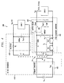
- the forward power converter 100 is an isolated version of the buck power converter previously discussed.
- the forward power converter 100 has an input coupled to a source of input power 110 and an output couplable to a load 150.
- the forward power converter 100 includes a primary inverter 120 having a primary side power switch Spri coupled to the input.
- the forward power converter 100 further includes an isolation transformer T1 having a primary winding P1 coupled to the primary side power switch Spri and secondary and reset windings S1, S2.
- the primary side power switch Spri conducts intermittently to transfer current from the input to the isolation transformer T1.
- a diode D1 coupled to the reset winding S2, cooperates therewith to reset the flux in the transformer T1 during a nonconduction period of the primary side power switch Spri.
- the diode D1 and reset winding S2 represent only one method for resetting the flux in the transformer T1 and that other methods of resetting the flux in the transformer T1 may also be employed.
- the forward power converter 100 further includes a rectifier 130 having an active switch Sw and a freewheeling diode Df coupled to the secondary winding S1.
- the active switch Sw conducts in synchronism with the primary side power switch Spri to transfer current to the output of the forward power converter 100.
- the forward power converter 100 still further includes an output filter 140 having an inductor L and an output capacitor Cout coupled to the rectifier 130.
- the freewheeling diode Df is reverse biased and power from the source of input power 110 is provided to both the inductor L and the load 150. Then, during the nonconduction period of the primary side power switch Spri, the active switch Sw opens, isolating the output from the secondary winding S1. The voltage impressed across the output filter 140 is, therefore, substantially zero during the nonconduction period of the primary side power switch Spri. Current now flows through the freewheeling diode Df to transfer some of the energy stored in the inductor L to the load 150.
- the output filter 140 filters and dampens the voltage fluctuations caused by the switching of the primary side power switch Spri and the active switch Sw to provide a substantially constant output voltage Vout at the output of the forward power converter 100.
- the freewheeling diode Df is adequate for power supplies that provide DC outputs, the freewheeling diode Df is a unidirectional device and thus is not capable of supporting four-quadrant operation.
- the present invention therefore, introduces a circulating capacitor employable (in a preferred embodiment) in power supplies capable of four-quadrant operation.
- FIGURE 2 illustrated is a schematic diagram of an embodiment of a power supply 200 constructed in accordance with the principles of the present invention.
- the power supply 200 has an input coupled to a source of input power 210 and an output couplable to a load 250.
- the power supply 200 includes a primary inverter 220 having a primary side power switch Spri coupled to the input.
- the power supply 200 further includes an isolation transformer T1 having a primary winding P1 coupled to the primary side power switch Spri and secondary and reset windings S1, S2.
- the primary side power switch Spri conducts intermittently to transfer current from the input to the isolation transformer T1.
- the primary inverter 220 operates analogously to the primary inverter 120 of the forward power converter 100 of FIGURE 1.
- the power supply 200 further includes a secondary side power switch Sw coupled to the secondary winding S1.
- the secondary side power switch Sw is operable to conduct within a conduction period of the primary side power switch to transfer current from the isolation transformer T1 to the output. In the illustrated embodiment, a portion of the current is contained within the power supply 200 during a nonconduction period of the secondary side power switch Sw.
- the power supply 200 therefore, further includes a capacitor (circulating capacitor Cf), coupled to the secondary side power switch Sw, that circulates the portion of the current toward the output during the nonconduction period of the secondary side power switch Sw.
- the power supply 200 further includes a resistor R coupled in series with the source of input power 210 and the circulating capacitor Cf. While the resistor R is illustrated as a discrete component, those skilled in the art realize that the resistor R may be a parasitic resistance of the secondary side power switch Sw.
- FIGURE 3 illustrated is a graph of a voltage Vcf across the circulating capacitor Cf of the power supply 200 of FIGURE 2.
- the power supply 200 operates as follows.
- the primary side power switch Spri conducts for a primary period D to impress the input voltage Vin across the isolation transformer T1.
- the primary side power switch Spri is nonconducting.
- the primary side power switch Spri thus develops an alternating voltage across the isolation transformer T1.
- the secondary side power switch Sw conducts within the primary period D or the auxiliary period 1-D (depending on a desired polarity of the output voltage) to impress the alternating voltage from the secondary winding S1 across the circulating capacitor Cf and the resistor R.
- the circulating capacitor Cf quickly charges to a portion of the alternating voltage from the secondary winding S1. (See FIGURE 3). Since the voltage Vcf across the circulating capacitor Cf may not always be equal to the alternating voltage from the secondary winding S1, the resistor R allows some energy to be dissipated. Then, during a nonconduction period 1-Dsec of the secondary side power switch Sw, the output is isolated from the alternating voltage at the isolation transformer T1. The circulating capacitor Cf now discharges to the load 250. The circulating capacitor Cf thus allows current to circulate toward the output during the nonconduction period 1-Dsec of the secondary side power switch Sw.
- the power supply 200 is therefore capable of supplying a bipolar output waveform at the output.
- FIGURE 4 illustrated is a schematic diagram of another embodiment of a power supply 400 constructed in accordance with the principles of the present invention.
- the power supply 400 includes a DC-DC converter 410 that receives a DC input voltage Vin at an input of the power supply 400 and generates a DC output voltage V DC at a first output of the power supply 400.
- the power supply 400 further includes a four-quadrant inverter 450, coupled to the DC-DC converter 410, that generates an AC output waveform having a voltage V AC at a second output of the power supply 400.
- a first load requiring a DC voltage is coupled to the first output.
- a second load requiring an AC voltage is coupled to the second output.
- the DC-DC converter 410 includes a primary inverter 420 (e.g., a full-bridge, half-bridge, forward, flyback, Sepic or Zeta inverter) having a primary side power switch Spri coupled to an input of the power supply 400.
- the DC-DC converter 410 further includes an isolation transformer T1 having a primary winding P1 coupled to the primary side power switch Spri and first and second secondary windings S1, S2.
- the DC-DC converter 410 further includes a rectifier 430 coupled to the first secondary winding S1.
- the rectifier 430 includes a rectifying diode Dr.
- the DC-DC converter 410 still further includes a first output capacitor Cout1 coupled to the rectifier 430.
- the DC-DC converter 410 provides the DC output voltage V DC at the first output of the power supply 400.
- the isolation transformer T1 has a second secondary winding S2.
- the four-quadrant inverter 450 is thus coupled to the DC-DC converter 410 via the second secondary winding S2.
- the present invention is also applicable to topologies having more than one transformer or to topologies without transformers.
- the four-quadrant inverter 450 includes a secondary side power switch Sa, coupled between the second secondary winding S2 and the second output of the power supply 400.
- the secondary side power switch Sa is a bidirectional switch having opposing first and second unidirectional switches, Sw1, Sw2.
- first and second unidirectional switches Sw1, Sw2 are illustrated as metal oxide semiconductor field-effect transistors (MOSFETs), those skilled in the art realize that the first and second unidirectional switches Sw1, Sw2 may be insulated gate bipolar junction transistors (IGBTs) or other conventional active switches.
- first and second unidirectional switches Sw1, Sw2 of the secondary side power switch Sa are hereinafter described as concurrently switched, those skilled in the art will realize that the first and second unidirectional switches Sw1, Sw2 may also be switched individually, based on a level of current therethrough.
- the four-quadrant inverter 450 further includes a circulating capacitor Cf coupled to the secondary side power switch Sa.
- the four-quadrant inverter 450 further includes a resistor R, series coupled to the secondary side power switch Sa. While the resistor R is illustrated as a separate element, those skilled in the art realize that the resistor R may be a parasitic resistance of the secondary side power switch Sa.
- the four-quadrant inverter 450 still further includes an output filter 460 having an inductor L and a second output capacitor Cout2. Alternatively, the output filter 460 may have a resistor in lieu of the inductor L. While the illustrated embodiment includes the output filter 460, those skilled in the art realize that the output filter 460 is not required to practice the present invention.
- the four-quadrant inverter 450 thus provides the AC output waveform at the second output of the power supply 400.
- Specific component values and output voltages are disclosed in the illustrated embodiment. Those skilled in the art will realize, of course, that the values shown are for illustrative purposes only and that the present invention is not restricted to such values and output voltages.
- the power supply 400 operates as follows.
- the primary side power switch Spri of the primary inverter 420 conducts intermittently to transfer current from the input of the DC-DC converter 410 to the isolation transformer T1.
- the primary side power switch Spri thus applies an alternating voltage across the primary winding P1.
- the primary inverter 420 is controlled by pulse-width modulation (PWM).
- PWM pulse-width modulation
- the alternating voltage therefore, exhibits a substantially rectangular and bipolar waveform.
- the isolation transformer T1 then conveys the alternating voltage between the primary winding P1 and the first and second secondary windings S1, S2.
- the rectifier 430 rectifies an alternating voltage waveform from the first secondary winding S1.
- the first output capacitor Cout1 then filters the rectified waveform to supply the DC output voltage V DC at the first output of the power supply 400.
- the duty cycle of the primary side power switch Spri is regulated to maintain the DC output voltage V DC at a substantially constant voltage.
- the primary inverter 420 may be free-running, providing an unregulated DC output voltage V DC .
- rectifiers having active switches may be also employed, the rectifier switching to regulate the DC output voltage V DC .
- the four-quadrant inverter 450 is coupled to the second secondary winding S2.
- the four-quadrant inverter 450 receives an alternating voltage from the second secondary winding S2 and develops therefrom an AC waveform.
- the alternating voltage from the second secondary winding S2 is at about a first frequency (e.g., 100 kHz) and exhibits both positive and negative voltages in each switching cycle of the primary inverter 420.
- the alternating voltage from the second secondary winding S2 may be substantially negative.
- the alternating voltage from the second secondary winding S2 may be substantially positive.
- the secondary side power switch Sa conducts to transfer a portion of the alternating voltage from the second secondary winding S2 to the output filter 460.
- the secondary side power switch Sa may, for example, conduct during the primary period D of the switching cycle to couple the negative voltage on the second secondary winding S2 to the output filter 460.
- the secondary side power switch Sa may conduct during the auxiliary period 1-D of the switching cycle to couple the positive voltage on the second secondary winding S2 to the output filter 460.
- the bi-directional switch Sa may conduct during both the primary and auxiliary periods D, 1-D of the switching cycle.
- the circulating capacitor Cf charges to a voltage that may be as large as the alternating voltage from the second secondary winding S2. Since the voltage Vcf across the circulating capacitor Cf may not initially be equal to the alternating voltage from the second secondary winding S2, some energy will be dissipated in the resistor R.
- the alternating voltage from the second secondary winding S2 provides power to both the inductor L and the second load. The second load establishes a current through both the second load and the inductor L. Then, during a nonconduction period of the secondary side power switch Sa, the alternating voltage from the second secondary winding S2 is isolated from the second output.
- the circulating capacitor Cf now discharges in a resonant manner through the inductor L to the second output capacitor Cout2 and the second load.
- the circulating capacitor Cf thus allows the current to circulate toward the second output during the nonconduction period of the secondary side power switch Sa.
- the output filter 460 then filters and dampens the voltage fluctuations caused by the switching of the secondary side power switch Sa to provide the AC output waveform.
Abstract
Description
- This application is related to the following applications:
Reference No. Title Inventor(s) Date Farrington 19-44-22-19 Dual Output Power Supply and Method of Operation Thereof Farrington, et al. Nov. 12, 1998 Jacobs 45-23-20 Controller for Power Supply and Method of Operation Thereof Jacobs, et al. Nov. 12, 1998 - The above-listed applications are commonly assigned with the present invention and are incorporated herein by reference as if reproduced herein in their entirety.
- The present invention is directed, in general, to power conversion and, more specifically, to a power supply employing a circulating capacitor for current circulation and a method of operating the same.
- A power converter is a power processing circuit that converts an input voltage waveform into a specified output voltage waveform. A switched-mode power converter is a frequently employed power converter that converts an input voltage waveform into a specified output voltage waveform. A buck power converter is one example of a switched-mode converter that converts the input voltage to an output voltage that is lower than the input voltage. Typically, the buck power converter is employed in applications wherein a stable, regulated voltage is desired at the output of the power converter.
- A buck power converter generally includes an active switch coupled to a source of input voltage. The active switch intermittently switches to provide an output voltage to a load at an output of the buck power converter. A controller regulates the output voltage by varying a duty cycle of the active switch. Depending on the duty cycle of the active switch, the output voltage may be regulated to any desired voltage between zero and the input voltage. Employing a high switching frequency in the power converter may cause ripple fluctuations in the output voltage. Conventional buck power converters, therefore, typically include a low pass output filter having an inductor and an output capacitor. The corner frequency of the output filter may be set sufficiently lower than the switching frequency of the active switch to minimize the ripple fluctuations.
- Since the active switch is coupled in series with the inductor, an inductor current is established during a conduction interval of the active switch. Opening the active switch may, therefore, result in a high voltage across the active switch unless an alternative path is provided for the inductor current. The problem of inductor current may be overcome by coupling a diode between the active switch and the inductor. During the conduction interval of the active switch, the diode is reversed biased. Then, during a nonconduction interval of the active switch, the inductor current flows through the diode, transferring some of its stored energy to the load. The buck power converter, like other switched-mode power converters, thus preferably includes at least two semiconductor switches, the active switch and the diode, to execute a switching cycle.
- A principal advantage of switched-mode power supplies is an improved power processing efficiency over other circuit approaches such as linear regulators. Switched-mode power supplies may also be required to operate in four quadrants (e.g., provide a bipolar output voltage or transmit power in either direction at the input or output). If four-quadrant operation is required, conventional switched-mode power supplies typically employ a bipolar source of input power and an auxiliary active switch in place of the diode. While the use of two active switches may enable four-quadrant operation, circuit complexity is increased. Further, unlike the active switches employed in the buck power converter previously discussed, the active switches of the four-quadrant power supply may be required to block or conduct currents in both directions. Since many commonly available active switches, such as field-effect transistors (FETs), provide only unidirectional current blocking, each active switch may consist of two series-coupled FETs. In addition to the increased costs of providing the two active switches, custom controllers may also be required to provide isolated drive signals to the control terminals of the active switches, further increasing the cost and complexity of the power supply.
- Accordingly, what is needed in the art is a current circulation device for a power supply and, additionally, a power supply that employs the current circulation device and is thus capable of bidirectional operation, thereby overcoming the high cost and complexities associated with the use of the two switches of the prior art.
- To address the above-discussed deficiencies of the prior art, the present invention provides a power supply and method of operation thereof. In one embodiment, the power supply includes: (1) a primary side power switch, (2) an isolation transformer having a primary winding coupled to the primary side power switch, the primary side power switch conducting intermittently to transfer current from an input of the power supply to the isolation transformer, (3) a secondary side power switch, coupled to a secondary winding of the isolation transformer, that is operable to conduct within a conduction period of the primary side power switch to transfer current from the isolation transformer to an output of the power supply, a portion of the current being contained within the power supply during a nonconduction period of the secondary side power switch and (4) a capacitor, coupled to the secondary side power switch, that circulates the portion toward the output during the nonconduction period.
- The present invention therefore introduces the broad concept of employing a capacitor for current circulation. In conventional power supplies that provide DC outputs, the capacitor may be employed in lieu of a diode for current circulation. The capacitor is, of course, capable of bi-directional operation and may advantageously be employed in four-quadrant switched-mode power supplies in lieu of an auxiliary bi-directional active switch. As a passive device, the capacitor avoids the high cost and complexities associated with the use of the bi-directional active switch.
- In one embodiment of the present invention, the power supply further includes an output capacitor coupled across the output. The output capacitor filters and smooths the output voltage, thus minimizing ripple fluctuations therein.
- In a related embodiment, the power supply further includes an inductor coupled to the output. In an alternative embodiment, the power supply further includes a filter resistor coupled to the output. The inductor or filter resistor filters the output voltage to minimize ripple fluctuations therein. Those skilled in the art will realize, of course, that neither the output capacitor, the inductor nor the filter resistor is necessary to practice the present invention.
- In one embodiment of the present invention, the power supply further includes a resistor series-coupled to the secondary side power switch. The resistor supplements a parasitic resistance of the secondary side power switch and reduces a peak current therethrough.
- In one embodiment of the present invention, the secondary side power switch is at least one metal oxide semiconductor field-effect transistor (MOSFET). In an alternative embodiment, the secondary side power switch is at least one insulated gate bipolar junction transistor (IGBT). Those skilled in the art are familiar with conventional active switches such as MOSFETs and IGBTs. Of course, the use of other active switches is well within the broad scope of the present invention.
- In one embodiment of the present invention, the input of the power supply is couplable to a source of direct current (DC) power. In an alternative embodiment, the input may be coupled to a DC-DC converter via an isolation transformer. In a related embodiment, the DC-DC converter includes a primary inverter selected from the group consisting of an asymmetrical half bridge, a half bridge, a full bridge, a forward, a flyback, a Sepic, and a Zeta. Conventional inverter topologies are familiar to those skilled in the art. Of course, the present invention is not limited to the inverter topologies disclosed herein. In another related embodiment, the DC-DC converter further includes a rectifier selected from the group consisting of a half wave rectifier, a full wave rectifier, a hybridge rectifier, a multiple transformer rectifier and a flyback rectifier. Those skilled in the art will realize, of course, that the use of other rectifier topologies is well within the broad scope of the present invention.
- The foregoing has outlined, rather broadly, preferred and alternative features of the present invention so that those skilled in the art may better understand the detailed description of the invention that follows. Additional features of the invention will be described hereinafter that form the subject of the claims of the invention. Those skilled in the art should appreciate that they can readily use the disclosed conception and specific embodiment as a basis for designing or modifying other structures for carrying out the same purposes of the present invention. Those skilled in the art should also realize that such equivalent constructions do not depart from the spirit and scope of the invention in its broadest form.
- For a more complete understanding of the present invention, reference is now made to the following descriptions taken in conjunction with the accompanying drawings, in which:
- FIGURE 1 illustrates a schematic diagram of a prior art forward power converter;
- FIGURE 2 illustrates a schematic diagram of an embodiment of a power supply constructed in accordance with the principles of the present invention;
- FIGURE 3 illustrates a graph of a voltage across the capacitor of the power supply of FIGURE 2; and
- FIGURE 4 illustrates a schematic diagram of another embodiment of a power supply constructed in accordance with the principles of the present invention.
-
- Referring initially to FIGURE 1, illustrated is a schematic diagram of a prior art forward
power converter 100. Theforward power converter 100 is an isolated version of the buck power converter previously discussed. Theforward power converter 100 has an input coupled to a source ofinput power 110 and an output couplable to aload 150. Theforward power converter 100 includes aprimary inverter 120 having a primary side power switch Spri coupled to the input. Theforward power converter 100 further includes an isolation transformer T1 having a primary winding P1 coupled to the primary side power switch Spri and secondary and reset windings S1, S2. The primary side power switch Spri conducts intermittently to transfer current from the input to the isolation transformer T1. A diode D1, coupled to the reset winding S2, cooperates therewith to reset the flux in the transformer T1 during a nonconduction period of the primary side power switch Spri. Those skilled in the art will realize that the diode D1 and reset winding S2 represent only one method for resetting the flux in the transformer T1 and that other methods of resetting the flux in the transformer T1 may also be employed. - The
forward power converter 100 further includes arectifier 130 having an active switch Sw and a freewheeling diode Df coupled to the secondary winding S1. In the illustrated embodiment, the active switch Sw conducts in synchronism with the primary side power switch Spri to transfer current to the output of theforward power converter 100. Theforward power converter 100 still further includes anoutput filter 140 having an inductor L and an output capacitor Cout coupled to therectifier 130. - During a conduction period of the primary side power switch Spri, the freewheeling diode Df is reverse biased and power from the source of
input power 110 is provided to both the inductor L and theload 150. Then, during the nonconduction period of the primary side power switch Spri, the active switch Sw opens, isolating the output from the secondary winding S1. The voltage impressed across theoutput filter 140 is, therefore, substantially zero during the nonconduction period of the primary side power switch Spri. Current now flows through the freewheeling diode Df to transfer some of the energy stored in the inductor L to theload 150. Theoutput filter 140 filters and dampens the voltage fluctuations caused by the switching of the primary side power switch Spri and the active switch Sw to provide a substantially constant output voltage Vout at the output of theforward power converter 100. - While the freewheeling diode Df is adequate for power supplies that provide DC outputs, the freewheeling diode Df is a unidirectional device and thus is not capable of supporting four-quadrant operation. The present invention, therefore, introduces a circulating capacitor employable (in a preferred embodiment) in power supplies capable of four-quadrant operation.
- Turning now to FIGURE 2, illustrated is a schematic diagram of an embodiment of a
power supply 200 constructed in accordance with the principles of the present invention. Thepower supply 200 has an input coupled to a source ofinput power 210 and an output couplable to aload 250. Thepower supply 200 includes a primary inverter 220 having a primary side power switch Spri coupled to the input. Thepower supply 200 further includes an isolation transformer T1 having a primary winding P1 coupled to the primary side power switch Spri and secondary and reset windings S1, S2. The primary side power switch Spri conducts intermittently to transfer current from the input to the isolation transformer T1. The primary inverter 220 operates analogously to theprimary inverter 120 of theforward power converter 100 of FIGURE 1. - The
power supply 200 further includes a secondary side power switch Sw coupled to the secondary winding S1. The secondary side power switch Sw is operable to conduct within a conduction period of the primary side power switch to transfer current from the isolation transformer T1 to the output. In the illustrated embodiment, a portion of the current is contained within thepower supply 200 during a nonconduction period of the secondary side power switch Sw. Thepower supply 200, therefore, further includes a capacitor (circulating capacitor Cf), coupled to the secondary side power switch Sw, that circulates the portion of the current toward the output during the nonconduction period of the secondary side power switch Sw. Thepower supply 200 further includes a resistor R coupled in series with the source ofinput power 210 and the circulating capacitor Cf. While the resistor R is illustrated as a discrete component, those skilled in the art realize that the resistor R may be a parasitic resistance of the secondary side power switch Sw. - Turning now to FIGURE 3, illustrated is a graph of a voltage Vcf across the circulating capacitor Cf of the
power supply 200 of FIGURE 2. With continuing reference to FIGURE 2, thepower supply 200 operates as follows. The primary side power switch Spri conducts for a primary period D to impress the input voltage Vin across the isolation transformer T1. Then, for an auxiliary period 1-D, the primary side power switch Spri is nonconducting. The primary side power switch Spri thus develops an alternating voltage across the isolation transformer T1. The secondary side power switch Sw conducts within the primary period D or the auxiliary period 1-D (depending on a desired polarity of the output voltage) to impress the alternating voltage from the secondary winding S1 across the circulating capacitor Cf and the resistor R. During a conduction period Dsec of the secondary side power switch Sw, the circulating capacitor Cf quickly charges to a portion of the alternating voltage from the secondary winding S1. (See FIGURE 3). Since the voltage Vcf across the circulating capacitor Cf may not always be equal to the alternating voltage from the secondary winding S1, the resistor R allows some energy to be dissipated. Then, during a nonconduction period 1-Dsec of the secondary side power switch Sw, the output is isolated from the alternating voltage at the isolation transformer T1. The circulating capacitor Cf now discharges to theload 250. The circulating capacitor Cf thus allows current to circulate toward the output during the nonconduction period 1-Dsec of the secondary side power switch Sw. Thepower supply 200 is therefore capable of supplying a bipolar output waveform at the output. - Turning now to FIGURE 4, illustrated is a schematic diagram of another embodiment of a
power supply 400 constructed in accordance with the principles of the present invention. Thepower supply 400 includes a DC-DC converter 410 that receives a DC input voltage Vin at an input of thepower supply 400 and generates a DC output voltage VDC at a first output of thepower supply 400. Conventional converter topologies are familiar to those skilled in the art and, as a result, the DC-DC converter 410 will not be described in detail. Thepower supply 400 further includes a four-quadrant inverter 450, coupled to the DC-DC converter 410, that generates an AC output waveform having a voltage VAC at a second output of thepower supply 400. In the illustrated embodiment, a first load requiring a DC voltage is coupled to the first output. A second load requiring an AC voltage is coupled to the second output. - The DC-
DC converter 410 includes a primary inverter 420 (e.g., a full-bridge, half-bridge, forward, flyback, Sepic or Zeta inverter) having a primary side power switch Spri coupled to an input of thepower supply 400. The DC-DC converter 410 further includes an isolation transformer T1 having a primary winding P1 coupled to the primary side power switch Spri and first and second secondary windings S1, S2. The DC-DC converter 410 further includes arectifier 430 coupled to the first secondary winding S1. In the illustrated embodiment, therectifier 430 includes a rectifying diode Dr. Of course, other rectifier topologies (e.g., a half wave rectifier, full wave rectifier, hybridge rectifier, multiple transformer rectifier or flyback rectifier) may also be advantageously employed with the principles of the present invention. The DC-DC converter 410 still further includes a first output capacitor Cout1 coupled to therectifier 430. The DC-DC converter 410 provides the DC output voltage VDC at the first output of thepower supply 400. - In the illustrated embodiment, the isolation transformer T1 has a second secondary winding S2. The four-
quadrant inverter 450 is thus coupled to the DC-DC converter 410 via the second secondary winding S2. Of course, the present invention is also applicable to topologies having more than one transformer or to topologies without transformers. - The four-
quadrant inverter 450 includes a secondary side power switch Sa, coupled between the second secondary winding S2 and the second output of thepower supply 400. In the illustrated embodiment, the secondary side power switch Sa is a bidirectional switch having opposing first and second unidirectional switches, Sw1, Sw2. Those skilled in the art will realize, of course, that other implementations of the secondary side power switch Sa are well within the broad scope of the present invention. Additionally, while the first and second unidirectional switches Sw1, Sw2 are illustrated as metal oxide semiconductor field-effect transistors (MOSFETs), those skilled in the art realize that the first and second unidirectional switches Sw1, Sw2 may be insulated gate bipolar junction transistors (IGBTs) or other conventional active switches. Further, while the first and second unidirectional switches Sw1, Sw2 of the secondary side power switch Sa are hereinafter described as concurrently switched, those skilled in the art will realize that the first and second unidirectional switches Sw1, Sw2 may also be switched individually, based on a level of current therethrough. - The four-
quadrant inverter 450 further includes a circulating capacitor Cf coupled to the secondary side power switch Sa. The four-quadrant inverter 450 further includes a resistor R, series coupled to the secondary side power switch Sa. While the resistor R is illustrated as a separate element, those skilled in the art realize that the resistor R may be a parasitic resistance of the secondary side power switch Sa. The four-quadrant inverter 450 still further includes anoutput filter 460 having an inductor L and a second output capacitor Cout2. Alternatively, theoutput filter 460 may have a resistor in lieu of the inductor L. While the illustrated embodiment includes theoutput filter 460, those skilled in the art realize that theoutput filter 460 is not required to practice the present invention. The four-quadrant inverter 450 thus provides the AC output waveform at the second output of thepower supply 400. Specific component values and output voltages are disclosed in the illustrated embodiment. Those skilled in the art will realize, of course, that the values shown are for illustrative purposes only and that the present invention is not restricted to such values and output voltages. - The
power supply 400 operates as follows. The primary side power switch Spri of theprimary inverter 420 conducts intermittently to transfer current from the input of the DC-DC converter 410 to the isolation transformer T1. The primary side power switch Spri thus applies an alternating voltage across the primary winding P1. In the illustrated embodiment, theprimary inverter 420 is controlled by pulse-width modulation (PWM). The alternating voltage, therefore, exhibits a substantially rectangular and bipolar waveform. Those skilled in the art are familiar with conventional PWM techniques and the waveforms resulting therefrom. The isolation transformer T1 then conveys the alternating voltage between the primary winding P1 and the first and second secondary windings S1, S2. - The
rectifier 430 rectifies an alternating voltage waveform from the first secondary winding S1. The first output capacitor Cout1 then filters the rectified waveform to supply the DC output voltage VDC at the first output of thepower supply 400. In one embodiment of the present invention, the duty cycle of the primary side power switch Spri is regulated to maintain the DC output voltage VDC at a substantially constant voltage. In another embodiment, theprimary inverter 420 may be free-running, providing an unregulated DC output voltage VDC. Of course, rectifiers having active switches may be also employed, the rectifier switching to regulate the DC output voltage VDC. - The four-
quadrant inverter 450 is coupled to the second secondary winding S2. The four-quadrant inverter 450 receives an alternating voltage from the second secondary winding S2 and develops therefrom an AC waveform. In the illustrated embodiment, the alternating voltage from the second secondary winding S2 is at about a first frequency (e.g., 100 kHz) and exhibits both positive and negative voltages in each switching cycle of theprimary inverter 420. For example, during a primary period D of the switching cycle, the alternating voltage from the second secondary winding S2 may be substantially negative. Then, during an auxiliary period 1-D of the switching cycle, the alternating voltage from the second secondary winding S2 may be substantially positive. The secondary side power switch Sa conducts to transfer a portion of the alternating voltage from the second secondary winding S2 to theoutput filter 460. The secondary side power switch Sa may, for example, conduct during the primary period D of the switching cycle to couple the negative voltage on the second secondary winding S2 to theoutput filter 460. Alternatively, the secondary side power switch Sa may conduct during the auxiliary period 1-D of the switching cycle to couple the positive voltage on the second secondary winding S2 to theoutput filter 460. Of course, the bi-directional switch Sa may conduct during both the primary and auxiliary periods D, 1-D of the switching cycle. - During the conduction period of the secondary side power switch Sa, the circulating capacitor Cf charges to a voltage that may be as large as the alternating voltage from the second secondary winding S2. Since the voltage Vcf across the circulating capacitor Cf may not initially be equal to the alternating voltage from the second secondary winding S2, some energy will be dissipated in the resistor R. The alternating voltage from the second secondary winding S2 provides power to both the inductor L and the second load. The second load establishes a current through both the second load and the inductor L. Then, during a nonconduction period of the secondary side power switch Sa, the alternating voltage from the second secondary winding S2 is isolated from the second output. The circulating capacitor Cf now discharges in a resonant manner through the inductor L to the second output capacitor Cout2 and the second load. The circulating capacitor Cf thus allows the current to circulate toward the second output during the nonconduction period of the secondary side power switch Sa. The
output filter 460 then filters and dampens the voltage fluctuations caused by the switching of the secondary side power switch Sa to provide the AC output waveform. - For a better understanding of power electronics, including power supplies and four-quadrant inverters, see Power Electronics: Converters, Applications and Design, by N. Mohan, T. M. Undeland and W. P. Robbins, John Wiley & Sons Publishing Company (1989); Power Electronics and Variable Frequency Drives, by B. K. Bose, IEEE Press (1997); Power Electronics: Circuits, Devices, and Applications, Second Edition, by M. H. Rashid, Prentice Hall (1993); and A New Family of Isolated Zero-Voltage-Switched Converters, by R. Farrington, M. M. Jovanovic and F. C. Lee, in Proceedings of the Power Electronics Society Conference (1991). The aforementioned references are incorporated herein by reference.
- Although the present invention has been described in detail, those skilled in the art should understand that they can make various changes, substitutions and alterations herein without departing from the spirit and scope of the invention in its broadest form.
Claims (11)
- A power supply, comprising:a primary side power switch;an isolation transformer having a primary winding coupled to said primary side power switch, said primary side power switch conducting intermittently to transfer current from an input of said power supply to said isolation transformer;a secondary side power switch, coupled to a secondary winding of said isolation transformer, that is operable to conduct within a conduction period of said primary side power switch to transfer current from said isolation transformer to an output of said power supply, a portion of said current being contained within said power supply during a nonconduction period of said secondary side power switch; anda capacitor, coupled to said secondary side power switch, that circulates said portion toward said output during said nonconduction period.
- The power supply as recited in Claim 1 further comprising a filter resistor coupled to said output.
- The power supply as recited in Claim 1 further comprising a resistor series-coupled to said secondary side power switch.
- A method of operating a power supply having a primary side power switch and an isolation transformer having a primary winding coupled to said primary side power switch, said primary side power switch conducting intermittently to transfer current from an input of said power supply to said isolation transformer, said method comprising:causing a secondary side power switch coupled to a secondary winding of said isolation transformer to conduct within a conduction period of said primary side power switch to transfer current from said isolation transformer to an output of said power supply, a portion of said current being contained within said power supply during a nonconduction period of said secondary side power switch; andcirculating said portion toward said output with a capacitor, coupled to said secondary side power switch, during said nonconduction period.
- The method as recited in Claim 4 further comprising filtering said current with a filter resistor coupled to said output.
- The method as recited in Claim 4 further comprising attenuating said current with a resistor series-coupled to said power switch.
- A power supply, comprising:a DC-DC converter including:a primary inverter having a primary side power switch,an isolation transformer having a primary winding coupled to said primary side power switch and first and second secondary windings, said primary side power switch conducting intermittently to transfer current from an input of said DC-DC converter to said isolation transformer; anda rectifier, coupled to said first secondary winding; anda four-quadrant inverter, coupled to said second secondary winding, including:a secondary side power switch, coupled to said second secondary winding, that is operable to conduct within a conduction period of said primary side power switch to transfer current from said isolation transformer to an output of said power supply, a portion of said current being contained within said power supply during a nonconduction period of said secondary side power switch; anda capacitor, coupled to said secondary side power switch, that circulates said portion toward said output during said nonconduction period.
- The power supply as recited in Claim 7 wherein said four-quadrant inverter further includes an output filter, coupled to said capacitor, that filters said current for delivery to said output.
- The power supply as recited in Claim 7 wherein said four-quadrant inverter further includes a resistor series-coupled to said secondary side power switch.
- The power supply as recited in Claim 7 wherein said primary inverter is selected from the group consisting of:an asymmetrical half bridge,a half bridge,a full bridge,a forward,a flyback,a Sepic, anda Zeta.
- The power supply as recited in Claim 7 wherein said rectifier is selected from the group consisting of:a half wave rectifier,a full wave rectifier,a hybridge rectifier,a multiple transformer rectifier, anda flyback rectifier.
Applications Claiming Priority (2)
| Application Number | Priority Date | Filing Date | Title |
|---|---|---|---|
| US191441 | 1998-11-12 | ||
| US09/191,441 US6038147A (en) | 1998-11-12 | 1998-11-12 | Power supply employing circulating capacitor and method of operation thereof |
Publications (2)
| Publication Number | Publication Date |
|---|---|
| EP1001516A2 true EP1001516A2 (en) | 2000-05-17 |
| EP1001516A3 EP1001516A3 (en) | 2001-12-12 |
Family
ID=22705525
Family Applications (1)
| Application Number | Title | Priority Date | Filing Date |
|---|---|---|---|
| EP99308669A Withdrawn EP1001516A3 (en) | 1998-11-12 | 1999-11-02 | Power supply employing circulating capacitor and method of operation thereof |
Country Status (3)
| Country | Link |
|---|---|
| US (1) | US6038147A (en) |
| EP (1) | EP1001516A3 (en) |
| JP (1) | JP2000152615A (en) |
Cited By (2)
| Publication number | Priority date | Publication date | Assignee | Title |
|---|---|---|---|---|
| WO2003041254A2 (en) * | 2001-11-05 | 2003-05-15 | Koninklijke Philips Electronics N.V. | Multiple-output flyback converter |
| WO2004100614A1 (en) * | 2003-05-07 | 2004-11-18 | Koninklijke Philips Electronics N.V. | Current control method and circuit for light emitting diodes |
Families Citing this family (12)
| Publication number | Priority date | Publication date | Assignee | Title |
|---|---|---|---|---|
| FR2773013B1 (en) * | 1997-12-23 | 2000-03-03 | Sextant Avionique | METHOD FOR CONTROLLING A CONTINUOUS-CONTINUOUS VOLTAGE CONVERTER WITH INDUCTIVE STORAGE |
| US6104623A (en) * | 1999-10-21 | 2000-08-15 | Lucent Technologies, Inc. | Multiple output converter having secondary regulator using self-driven synchronous rectifiers |
| DE10110239A1 (en) * | 2001-01-24 | 2002-07-25 | Patent Treuhand Ges Fuer Elektrische Gluehlampen Mbh | Electronic operating device for lamps with SEPIC converters, has first stage designed as SEPIC converter with time discrete regulation with control intervals longer than half mains period |
| CN100555829C (en) * | 2005-03-11 | 2009-10-28 | Nxp股份有限公司 | Switched mode power converter and method of operating thereof |
| US9036538B2 (en) | 2005-04-19 | 2015-05-19 | Qualcomm Incorporated | Frequency hopping design for single carrier FDMA systems |
| JP4320336B2 (en) * | 2006-10-24 | 2009-08-26 | Tdk株式会社 | Switching power supply |
| JP5783796B2 (en) | 2010-05-26 | 2015-09-24 | 株式会社半導体エネルギー研究所 | Photoelectric conversion device |
| JP2012015491A (en) | 2010-06-04 | 2012-01-19 | Semiconductor Energy Lab Co Ltd | Photoelectric conversion device |
| US8493126B2 (en) * | 2010-07-15 | 2013-07-23 | Qualcomm Incorporated | Wideband balun having a single primary and multiple secondaries |
| US8598737B2 (en) | 2010-12-13 | 2013-12-03 | Light-Based Technologies Incorporated | Synchronous switching power supply |
| KR101443760B1 (en) | 2013-11-28 | 2014-09-29 | 동양하이테크산업주식회사 | Switching mode power supply using on chip micro transformer |
| CN104852587B (en) * | 2015-06-03 | 2018-02-16 | 矽力杰半导体技术(杭州)有限公司 | Switched mode converter |
Citations (6)
| Publication number | Priority date | Publication date | Assignee | Title |
|---|---|---|---|---|
| DE2714152A1 (en) * | 1977-03-30 | 1978-10-12 | Siemens Ag | Static inverter generating pulses of alternate polarity - uses switched power transistors feeding pulse-shaping integrator |
| GB2087171A (en) * | 1980-11-05 | 1982-05-19 | Chloride Group Ltd | Static inverter |
| US4675797A (en) * | 1985-11-06 | 1987-06-23 | Vicor Corporation | Current-fed, forward converter switching at zero current |
| US4788634A (en) * | 1987-06-22 | 1988-11-29 | Massachusetts Institute Of Technology | Resonant forward converter |
| US5057986A (en) * | 1990-03-12 | 1991-10-15 | Unisys Corporation | Zero-voltage resonant transition switching power converter |
| US5742496A (en) * | 1995-10-31 | 1998-04-21 | Nec Corporation | Invertor apparatus for converting a DC voltage to a single-phase AC voltage |
Family Cites Families (10)
| Publication number | Priority date | Publication date | Assignee | Title |
|---|---|---|---|---|
| US3573597A (en) * | 1969-12-29 | 1971-04-06 | Gen Electric | High current switching regulator with overlapped output current pulses |
| US3839668A (en) * | 1973-06-13 | 1974-10-01 | Bell Northern Research Ltd | Electronic converter with regulated output current and frequency |
| US4357524A (en) * | 1980-01-29 | 1982-11-02 | Westinghouse Electric Corp. | Electrical heater controller for aircraft window heat control |
| US4785387A (en) * | 1986-04-28 | 1988-11-15 | Virginia Tech Intellectual Properties, Inc. | Resonant converters with secondary-side resonance |
| US4841220A (en) * | 1987-09-23 | 1989-06-20 | Tabisz Wojciech A | Dc-to-Dc converters using multi-resonant switches |
| US4866585A (en) * | 1988-06-08 | 1989-09-12 | Das Pawan K | AC to DC solid state power supply using high frequency pulsed power switching |
| US5291385A (en) * | 1992-04-02 | 1994-03-01 | Vlt Corporation | Zero-current switching forward power converter operating in damped reverse boost mode |
| US5623397A (en) * | 1994-01-27 | 1997-04-22 | Vlt Corporation | Power conversion in anticipatory reverse boost mode |
| KR0144540B1 (en) * | 1994-08-25 | 1998-10-01 | 김광호 | Surge protection circuit of smps |
| US5774351A (en) * | 1996-05-21 | 1998-06-30 | National Science Council | Series resonant DC-to-AC inverter system |
-
1998
- 1998-11-12 US US09/191,441 patent/US6038147A/en not_active Expired - Fee Related
-
1999
- 1999-11-02 EP EP99308669A patent/EP1001516A3/en not_active Withdrawn
- 1999-11-12 JP JP11321873A patent/JP2000152615A/en active Pending
Patent Citations (6)
| Publication number | Priority date | Publication date | Assignee | Title |
|---|---|---|---|---|
| DE2714152A1 (en) * | 1977-03-30 | 1978-10-12 | Siemens Ag | Static inverter generating pulses of alternate polarity - uses switched power transistors feeding pulse-shaping integrator |
| GB2087171A (en) * | 1980-11-05 | 1982-05-19 | Chloride Group Ltd | Static inverter |
| US4675797A (en) * | 1985-11-06 | 1987-06-23 | Vicor Corporation | Current-fed, forward converter switching at zero current |
| US4788634A (en) * | 1987-06-22 | 1988-11-29 | Massachusetts Institute Of Technology | Resonant forward converter |
| US5057986A (en) * | 1990-03-12 | 1991-10-15 | Unisys Corporation | Zero-voltage resonant transition switching power converter |
| US5742496A (en) * | 1995-10-31 | 1998-04-21 | Nec Corporation | Invertor apparatus for converting a DC voltage to a single-phase AC voltage |
Non-Patent Citations (2)
| Title |
|---|
| CHUNG Y H ET AL: "BILATERAL SERIES RESONANT INVERTER FOR HIGH FREQUENCY LINK UPS" IEE PROCEEDINGS B. ELECTRICAL POWER APPLICATIONS, INSTITUTION OF ELECTRICAL ENGINEERS. STEVENAGE, GB, vol. 138, no. 4 PART B, 1 July 1991 (1991-07-01), pages 159-166, XP000240570 * |
| LO D S ET AL: "A COMPACT DC-TO-DC POWER CONVERTER FOR DISTRIBUTED POWER PROCESSING" PROCEEDINGS OF THE ANNUAL APPLIED POWER ELECTRONICS CONFERENCE AND EXPOSITION. (APEC),US,NEW YORK, IEEE, vol. CONF. 5, 11 March 1990 (1990-03-11), pages 33-42, XP000143281 * |
Cited By (5)
| Publication number | Priority date | Publication date | Assignee | Title |
|---|---|---|---|---|
| WO2003041254A2 (en) * | 2001-11-05 | 2003-05-15 | Koninklijke Philips Electronics N.V. | Multiple-output flyback converter |
| WO2003041254A3 (en) * | 2001-11-05 | 2003-10-16 | Koninkl Philips Electronics Nv | Multiple-output flyback converter |
| WO2004100614A1 (en) * | 2003-05-07 | 2004-11-18 | Koninklijke Philips Electronics N.V. | Current control method and circuit for light emitting diodes |
| US7511436B2 (en) | 2003-05-07 | 2009-03-31 | Koninklijke Philips Electronics N.V. | Current control method and circuit for light emitting diodes |
| KR101160588B1 (en) * | 2003-05-07 | 2013-11-27 | 코닌클리케 필립스 엔.브이. | Current control method and circuit for light emitting diodes |
Also Published As
| Publication number | Publication date |
|---|---|
| US6038147A (en) | 2000-03-14 |
| EP1001516A3 (en) | 2001-12-12 |
| JP2000152615A (en) | 2000-05-30 |
Similar Documents
| Publication | Publication Date | Title |
|---|---|---|
| US6831847B2 (en) | Synchronous rectifier drive circuit and power supply including same | |
| US6201719B1 (en) | Controller for power supply and method of operation thereof | |
| US6069798A (en) | Asymmetrical power converter and method of operation thereof | |
| US6570268B1 (en) | Synchronous rectifier drive circuit and power supply including same | |
| Panov et al. | Design and performance evaluation of low-voltage/high-current DC/DC on-board modules | |
| US9812977B2 (en) | Resonant converters with an improved voltage regulation range | |
| US6058026A (en) | Multiple output converter having a single transformer winding and independent output regulation | |
| US8520414B2 (en) | Controller for a power converter | |
| US8488355B2 (en) | Driver for a synchronous rectifier and power converter employing the same | |
| US6246592B1 (en) | Unique power supply architecture with cascaded converters for large input-to-output step-down ratio | |
| US9118259B2 (en) | Phase-shifted dual-bridge DC/DC converter with wide-range ZVS and zero circulating current | |
| US7830684B2 (en) | Reverse biasing active snubber | |
| EP2421137B1 (en) | Switching power supply unit | |
| US6545883B2 (en) | Integrated boost-asymmetrical half-bridge converter | |
| US6191960B1 (en) | Active clamp for isolated power converter and method of operating thereof | |
| US6344768B1 (en) | Full-bridge DC-to-DC converter having an unipolar gate drive | |
| US6038147A (en) | Power supply employing circulating capacitor and method of operation thereof | |
| CN107431438B (en) | Switched mode power supply including a primary side clamp circuit controlled based on a secondary side signal | |
| EP1229635B1 (en) | Active gate clamp circuit for self driven synchronous rectifiers | |
| US6980447B1 (en) | Active snubber circuit for synchronous rectifier | |
| US6104623A (en) | Multiple output converter having secondary regulator using self-driven synchronous rectifiers | |
| US11075582B2 (en) | Switching converter | |
| US20020110010A1 (en) | Reverse recovery circuit, method of operation thereof and asymmetrical half-bridge power converter | |
| JP4605532B2 (en) | Multi-output type switching power supply | |
| Rodriguez et al. | A novel adaptive synchronous rectification system for low output voltage isolated converters |
Legal Events
| Date | Code | Title | Description |
|---|---|---|---|
| PUAI | Public reference made under article 153(3) epc to a published international application that has entered the european phase |
Free format text: ORIGINAL CODE: 0009012 |
|
| AK | Designated contracting states |
Kind code of ref document: A2 Designated state(s): AT BE CH CY DE DK ES FI FR GB GR IE IT LI LU MC NL PT SE |
|
| AX | Request for extension of the european patent |
Free format text: AL;LT;LV;MK;RO;SI |
|
| PUAL | Search report despatched |
Free format text: ORIGINAL CODE: 0009013 |
|
| AK | Designated contracting states |
Kind code of ref document: A3 Designated state(s): AT BE CH CY DE DK ES FI FR GB GR IE IT LI LU MC NL PT SE |
|
| AX | Request for extension of the european patent |
Free format text: AL;LT;LV;MK;RO;SI |
|
| AKX | Designation fees paid | ||
| REG | Reference to a national code |
Ref country code: DE Ref legal event code: 8566 |
|
| STAA | Information on the status of an ep patent application or granted ep patent |
Free format text: STATUS: THE APPLICATION IS DEEMED TO BE WITHDRAWN |
|
| 18D | Application deemed to be withdrawn |
Effective date: 20020602 |