EP1003214A2 - Semiconductor device and method of producing the same - Google Patents
Semiconductor device and method of producing the same Download PDFInfo
- Publication number
- EP1003214A2 EP1003214A2 EP99304340A EP99304340A EP1003214A2 EP 1003214 A2 EP1003214 A2 EP 1003214A2 EP 99304340 A EP99304340 A EP 99304340A EP 99304340 A EP99304340 A EP 99304340A EP 1003214 A2 EP1003214 A2 EP 1003214A2
- Authority
- EP
- European Patent Office
- Prior art keywords
- wiring board
- semiconductor device
- sealing resin
- heat spreading
- spreading plate
- Prior art date
- Legal status (The legal status is an assumption and is not a legal conclusion. Google has not performed a legal analysis and makes no representation as to the accuracy of the status listed.)
- Withdrawn
Links
Images


Classifications
-
- H—ELECTRICITY
- H01—ELECTRIC ELEMENTS
- H01L—SEMICONDUCTOR DEVICES NOT COVERED BY CLASS H10
- H01L24/00—Arrangements for connecting or disconnecting semiconductor or solid-state bodies; Methods or apparatus related thereto
- H01L24/01—Means for bonding being attached to, or being formed on, the surface to be connected, e.g. chip-to-package, die-attach, "first-level" interconnects; Manufacturing methods related thereto
- H01L24/26—Layer connectors, e.g. plate connectors, solder or adhesive layers; Manufacturing methods related thereto
- H01L24/31—Structure, shape, material or disposition of the layer connectors after the connecting process
- H01L24/32—Structure, shape, material or disposition of the layer connectors after the connecting process of an individual layer connector
-
- H—ELECTRICITY
- H04—ELECTRIC COMMUNICATION TECHNIQUE
- H04N—PICTORIAL COMMUNICATION, e.g. TELEVISION
- H04N23/00—Cameras or camera modules comprising electronic image sensors; Control thereof
- H04N23/50—Constructional details
- H04N23/54—Mounting of pick-up tubes, electronic image sensors, deviation or focusing coils
-
- H—ELECTRICITY
- H01—ELECTRIC ELEMENTS
- H01L—SEMICONDUCTOR DEVICES NOT COVERED BY CLASS H10
- H01L23/00—Details of semiconductor or other solid state devices
- H01L23/28—Encapsulations, e.g. encapsulating layers, coatings, e.g. for protection
- H01L23/31—Encapsulations, e.g. encapsulating layers, coatings, e.g. for protection characterised by the arrangement or shape
- H01L23/3107—Encapsulations, e.g. encapsulating layers, coatings, e.g. for protection characterised by the arrangement or shape the device being completely enclosed
- H01L23/3121—Encapsulations, e.g. encapsulating layers, coatings, e.g. for protection characterised by the arrangement or shape the device being completely enclosed a substrate forming part of the encapsulation
- H01L23/3128—Encapsulations, e.g. encapsulating layers, coatings, e.g. for protection characterised by the arrangement or shape the device being completely enclosed a substrate forming part of the encapsulation the substrate having spherical bumps for external connection
-
- H—ELECTRICITY
- H01—ELECTRIC ELEMENTS
- H01L—SEMICONDUCTOR DEVICES NOT COVERED BY CLASS H10
- H01L23/00—Details of semiconductor or other solid state devices
- H01L23/34—Arrangements for cooling, heating, ventilating or temperature compensation ; Temperature sensing arrangements
- H01L23/36—Selection of materials, or shaping, to facilitate cooling or heating, e.g. heatsinks
-
- H—ELECTRICITY
- H04—ELECTRIC COMMUNICATION TECHNIQUE
- H04N—PICTORIAL COMMUNICATION, e.g. TELEVISION
- H04N23/00—Cameras or camera modules comprising electronic image sensors; Control thereof
- H04N23/50—Constructional details
- H04N23/55—Optical parts specially adapted for electronic image sensors; Mounting thereof
-
- H—ELECTRICITY
- H01—ELECTRIC ELEMENTS
- H01L—SEMICONDUCTOR DEVICES NOT COVERED BY CLASS H10
- H01L2224/00—Indexing scheme for arrangements for connecting or disconnecting semiconductor or solid-state bodies and methods related thereto as covered by H01L24/00
- H01L2224/01—Means for bonding being attached to, or being formed on, the surface to be connected, e.g. chip-to-package, die-attach, "first-level" interconnects; Manufacturing methods related thereto
- H01L2224/02—Bonding areas; Manufacturing methods related thereto
- H01L2224/04—Structure, shape, material or disposition of the bonding areas prior to the connecting process
- H01L2224/05—Structure, shape, material or disposition of the bonding areas prior to the connecting process of an individual bonding area
- H01L2224/0554—External layer
- H01L2224/05599—Material
-
- H—ELECTRICITY
- H01—ELECTRIC ELEMENTS
- H01L—SEMICONDUCTOR DEVICES NOT COVERED BY CLASS H10
- H01L2224/00—Indexing scheme for arrangements for connecting or disconnecting semiconductor or solid-state bodies and methods related thereto as covered by H01L24/00
- H01L2224/01—Means for bonding being attached to, or being formed on, the surface to be connected, e.g. chip-to-package, die-attach, "first-level" interconnects; Manufacturing methods related thereto
- H01L2224/26—Layer connectors, e.g. plate connectors, solder or adhesive layers; Manufacturing methods related thereto
- H01L2224/31—Structure, shape, material or disposition of the layer connectors after the connecting process
- H01L2224/32—Structure, shape, material or disposition of the layer connectors after the connecting process of an individual layer connector
- H01L2224/3205—Shape
- H01L2224/32057—Shape in side view
-
- H—ELECTRICITY
- H01—ELECTRIC ELEMENTS
- H01L—SEMICONDUCTOR DEVICES NOT COVERED BY CLASS H10
- H01L2224/00—Indexing scheme for arrangements for connecting or disconnecting semiconductor or solid-state bodies and methods related thereto as covered by H01L24/00
- H01L2224/01—Means for bonding being attached to, or being formed on, the surface to be connected, e.g. chip-to-package, die-attach, "first-level" interconnects; Manufacturing methods related thereto
- H01L2224/26—Layer connectors, e.g. plate connectors, solder or adhesive layers; Manufacturing methods related thereto
- H01L2224/31—Structure, shape, material or disposition of the layer connectors after the connecting process
- H01L2224/32—Structure, shape, material or disposition of the layer connectors after the connecting process of an individual layer connector
- H01L2224/321—Disposition
- H01L2224/32151—Disposition the layer connector connecting between a semiconductor or solid-state body and an item not being a semiconductor or solid-state body, e.g. chip-to-substrate, chip-to-passive
- H01L2224/32221—Disposition the layer connector connecting between a semiconductor or solid-state body and an item not being a semiconductor or solid-state body, e.g. chip-to-substrate, chip-to-passive the body and the item being stacked
- H01L2224/32225—Disposition the layer connector connecting between a semiconductor or solid-state body and an item not being a semiconductor or solid-state body, e.g. chip-to-substrate, chip-to-passive the body and the item being stacked the item being non-metallic, e.g. insulating substrate with or without metallisation
-
- H—ELECTRICITY
- H01—ELECTRIC ELEMENTS
- H01L—SEMICONDUCTOR DEVICES NOT COVERED BY CLASS H10
- H01L2224/00—Indexing scheme for arrangements for connecting or disconnecting semiconductor or solid-state bodies and methods related thereto as covered by H01L24/00
- H01L2224/01—Means for bonding being attached to, or being formed on, the surface to be connected, e.g. chip-to-package, die-attach, "first-level" interconnects; Manufacturing methods related thereto
- H01L2224/42—Wire connectors; Manufacturing methods related thereto
- H01L2224/47—Structure, shape, material or disposition of the wire connectors after the connecting process
- H01L2224/48—Structure, shape, material or disposition of the wire connectors after the connecting process of an individual wire connector
- H01L2224/4805—Shape
- H01L2224/4809—Loop shape
- H01L2224/48091—Arched
-
- H—ELECTRICITY
- H01—ELECTRIC ELEMENTS
- H01L—SEMICONDUCTOR DEVICES NOT COVERED BY CLASS H10
- H01L2224/00—Indexing scheme for arrangements for connecting or disconnecting semiconductor or solid-state bodies and methods related thereto as covered by H01L24/00
- H01L2224/01—Means for bonding being attached to, or being formed on, the surface to be connected, e.g. chip-to-package, die-attach, "first-level" interconnects; Manufacturing methods related thereto
- H01L2224/42—Wire connectors; Manufacturing methods related thereto
- H01L2224/47—Structure, shape, material or disposition of the wire connectors after the connecting process
- H01L2224/48—Structure, shape, material or disposition of the wire connectors after the connecting process of an individual wire connector
- H01L2224/481—Disposition
- H01L2224/48151—Connecting between a semiconductor or solid-state body and an item not being a semiconductor or solid-state body, e.g. chip-to-substrate, chip-to-passive
- H01L2224/48221—Connecting between a semiconductor or solid-state body and an item not being a semiconductor or solid-state body, e.g. chip-to-substrate, chip-to-passive the body and the item being stacked
- H01L2224/48225—Connecting between a semiconductor or solid-state body and an item not being a semiconductor or solid-state body, e.g. chip-to-substrate, chip-to-passive the body and the item being stacked the item being non-metallic, e.g. insulating substrate with or without metallisation
- H01L2224/48227—Connecting between a semiconductor or solid-state body and an item not being a semiconductor or solid-state body, e.g. chip-to-substrate, chip-to-passive the body and the item being stacked the item being non-metallic, e.g. insulating substrate with or without metallisation connecting the wire to a bond pad of the item
-
- H—ELECTRICITY
- H01—ELECTRIC ELEMENTS
- H01L—SEMICONDUCTOR DEVICES NOT COVERED BY CLASS H10
- H01L2224/00—Indexing scheme for arrangements for connecting or disconnecting semiconductor or solid-state bodies and methods related thereto as covered by H01L24/00
- H01L2224/01—Means for bonding being attached to, or being formed on, the surface to be connected, e.g. chip-to-package, die-attach, "first-level" interconnects; Manufacturing methods related thereto
- H01L2224/42—Wire connectors; Manufacturing methods related thereto
- H01L2224/47—Structure, shape, material or disposition of the wire connectors after the connecting process
- H01L2224/48—Structure, shape, material or disposition of the wire connectors after the connecting process of an individual wire connector
- H01L2224/484—Connecting portions
- H01L2224/48463—Connecting portions the connecting portion on the bonding area of the semiconductor or solid-state body being a ball bond
- H01L2224/48465—Connecting portions the connecting portion on the bonding area of the semiconductor or solid-state body being a ball bond the other connecting portion not on the bonding area being a wedge bond, i.e. ball-to-wedge, regular stitch
-
- H—ELECTRICITY
- H01—ELECTRIC ELEMENTS
- H01L—SEMICONDUCTOR DEVICES NOT COVERED BY CLASS H10
- H01L2224/00—Indexing scheme for arrangements for connecting or disconnecting semiconductor or solid-state bodies and methods related thereto as covered by H01L24/00
- H01L2224/73—Means for bonding being of different types provided for in two or more of groups H01L2224/10, H01L2224/18, H01L2224/26, H01L2224/34, H01L2224/42, H01L2224/50, H01L2224/63, H01L2224/71
- H01L2224/732—Location after the connecting process
- H01L2224/73251—Location after the connecting process on different surfaces
- H01L2224/73265—Layer and wire connectors
-
- H—ELECTRICITY
- H01—ELECTRIC ELEMENTS
- H01L—SEMICONDUCTOR DEVICES NOT COVERED BY CLASS H10
- H01L2224/00—Indexing scheme for arrangements for connecting or disconnecting semiconductor or solid-state bodies and methods related thereto as covered by H01L24/00
- H01L2224/80—Methods for connecting semiconductor or other solid state bodies using means for bonding being attached to, or being formed on, the surface to be connected
- H01L2224/83—Methods for connecting semiconductor or other solid state bodies using means for bonding being attached to, or being formed on, the surface to be connected using a layer connector
- H01L2224/8338—Bonding interfaces outside the semiconductor or solid-state body
- H01L2224/83385—Shape, e.g. interlocking features
-
- H—ELECTRICITY
- H01—ELECTRIC ELEMENTS
- H01L—SEMICONDUCTOR DEVICES NOT COVERED BY CLASS H10
- H01L2224/00—Indexing scheme for arrangements for connecting or disconnecting semiconductor or solid-state bodies and methods related thereto as covered by H01L24/00
- H01L2224/80—Methods for connecting semiconductor or other solid state bodies using means for bonding being attached to, or being formed on, the surface to be connected
- H01L2224/85—Methods for connecting semiconductor or other solid state bodies using means for bonding being attached to, or being formed on, the surface to be connected using a wire connector
- H01L2224/8538—Bonding interfaces outside the semiconductor or solid-state body
- H01L2224/85399—Material
-
- H—ELECTRICITY
- H01—ELECTRIC ELEMENTS
- H01L—SEMICONDUCTOR DEVICES NOT COVERED BY CLASS H10
- H01L24/00—Arrangements for connecting or disconnecting semiconductor or solid-state bodies; Methods or apparatus related thereto
- H01L24/01—Means for bonding being attached to, or being formed on, the surface to be connected, e.g. chip-to-package, die-attach, "first-level" interconnects; Manufacturing methods related thereto
- H01L24/42—Wire connectors; Manufacturing methods related thereto
- H01L24/47—Structure, shape, material or disposition of the wire connectors after the connecting process
- H01L24/48—Structure, shape, material or disposition of the wire connectors after the connecting process of an individual wire connector
-
- H—ELECTRICITY
- H01—ELECTRIC ELEMENTS
- H01L—SEMICONDUCTOR DEVICES NOT COVERED BY CLASS H10
- H01L2924/00—Indexing scheme for arrangements or methods for connecting or disconnecting semiconductor or solid-state bodies as covered by H01L24/00
- H01L2924/0001—Technical content checked by a classifier
- H01L2924/00014—Technical content checked by a classifier the subject-matter covered by the group, the symbol of which is combined with the symbol of this group, being disclosed without further technical details
-
- H—ELECTRICITY
- H01—ELECTRIC ELEMENTS
- H01L—SEMICONDUCTOR DEVICES NOT COVERED BY CLASS H10
- H01L2924/00—Indexing scheme for arrangements or methods for connecting or disconnecting semiconductor or solid-state bodies as covered by H01L24/00
- H01L2924/01—Chemical elements
- H01L2924/01005—Boron [B]
-
- H—ELECTRICITY
- H01—ELECTRIC ELEMENTS
- H01L—SEMICONDUCTOR DEVICES NOT COVERED BY CLASS H10
- H01L2924/00—Indexing scheme for arrangements or methods for connecting or disconnecting semiconductor or solid-state bodies as covered by H01L24/00
- H01L2924/01—Chemical elements
- H01L2924/01006—Carbon [C]
-
- H—ELECTRICITY
- H01—ELECTRIC ELEMENTS
- H01L—SEMICONDUCTOR DEVICES NOT COVERED BY CLASS H10
- H01L2924/00—Indexing scheme for arrangements or methods for connecting or disconnecting semiconductor or solid-state bodies as covered by H01L24/00
- H01L2924/01—Chemical elements
- H01L2924/01013—Aluminum [Al]
-
- H—ELECTRICITY
- H01—ELECTRIC ELEMENTS
- H01L—SEMICONDUCTOR DEVICES NOT COVERED BY CLASS H10
- H01L2924/00—Indexing scheme for arrangements or methods for connecting or disconnecting semiconductor or solid-state bodies as covered by H01L24/00
- H01L2924/01—Chemical elements
- H01L2924/01029—Copper [Cu]
-
- H—ELECTRICITY
- H01—ELECTRIC ELEMENTS
- H01L—SEMICONDUCTOR DEVICES NOT COVERED BY CLASS H10
- H01L2924/00—Indexing scheme for arrangements or methods for connecting or disconnecting semiconductor or solid-state bodies as covered by H01L24/00
- H01L2924/01—Chemical elements
- H01L2924/01033—Arsenic [As]
-
- H—ELECTRICITY
- H01—ELECTRIC ELEMENTS
- H01L—SEMICONDUCTOR DEVICES NOT COVERED BY CLASS H10
- H01L2924/00—Indexing scheme for arrangements or methods for connecting or disconnecting semiconductor or solid-state bodies as covered by H01L24/00
- H01L2924/01—Chemical elements
- H01L2924/01061—Promethium [Pm]
-
- H—ELECTRICITY
- H01—ELECTRIC ELEMENTS
- H01L—SEMICONDUCTOR DEVICES NOT COVERED BY CLASS H10
- H01L2924/00—Indexing scheme for arrangements or methods for connecting or disconnecting semiconductor or solid-state bodies as covered by H01L24/00
- H01L2924/01—Chemical elements
- H01L2924/01078—Platinum [Pt]
-
- H—ELECTRICITY
- H01—ELECTRIC ELEMENTS
- H01L—SEMICONDUCTOR DEVICES NOT COVERED BY CLASS H10
- H01L2924/00—Indexing scheme for arrangements or methods for connecting or disconnecting semiconductor or solid-state bodies as covered by H01L24/00
- H01L2924/10—Details of semiconductor or other solid state devices to be connected
- H01L2924/11—Device type
- H01L2924/12—Passive devices, e.g. 2 terminal devices
- H01L2924/1204—Optical Diode
- H01L2924/12042—LASER
-
- H—ELECTRICITY
- H01—ELECTRIC ELEMENTS
- H01L—SEMICONDUCTOR DEVICES NOT COVERED BY CLASS H10
- H01L2924/00—Indexing scheme for arrangements or methods for connecting or disconnecting semiconductor or solid-state bodies as covered by H01L24/00
- H01L2924/15—Details of package parts other than the semiconductor or other solid state devices to be connected
- H01L2924/151—Die mounting substrate
- H01L2924/153—Connection portion
- H01L2924/1531—Connection portion the connection portion being formed only on the surface of the substrate opposite to the die mounting surface
- H01L2924/15311—Connection portion the connection portion being formed only on the surface of the substrate opposite to the die mounting surface being a ball array, e.g. BGA
-
- H—ELECTRICITY
- H01—ELECTRIC ELEMENTS
- H01L—SEMICONDUCTOR DEVICES NOT COVERED BY CLASS H10
- H01L2924/00—Indexing scheme for arrangements or methods for connecting or disconnecting semiconductor or solid-state bodies as covered by H01L24/00
- H01L2924/15—Details of package parts other than the semiconductor or other solid state devices to be connected
- H01L2924/151—Die mounting substrate
- H01L2924/153—Connection portion
- H01L2924/1532—Connection portion the connection portion being formed on the die mounting surface of the substrate
-
- H—ELECTRICITY
- H01—ELECTRIC ELEMENTS
- H01L—SEMICONDUCTOR DEVICES NOT COVERED BY CLASS H10
- H01L2924/00—Indexing scheme for arrangements or methods for connecting or disconnecting semiconductor or solid-state bodies as covered by H01L24/00
- H01L2924/15—Details of package parts other than the semiconductor or other solid state devices to be connected
- H01L2924/181—Encapsulation
Definitions
- the present invention generally relates to a semiconductor device and a method of producing the semiconductor device. More particularly, the present invention relates to a semiconductor device suitable for mounting a semiconductor chip which generates heat during an operation and to a method producing such a semiconductor device.
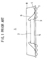
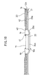
- Fig. 1 illustrates a conventional fine-pitch type semiconductor device 1.
- This semiconductor device 1 has a package structure called FBGA (Fine-pitch Ball Grid Array).
- FBGA Fe-pitch Ball Grid Array
- This structure includes a semiconductor chip 2, a wiring board 3, solder balls 7, and a sealing resin 8.
- the semiconductor chip 2 has a high density, and is fixed with an adhesive 5 onto the upper surface of the wiring board 3, which functions as an interposer.
- the wiring board 3 is a printed wiring board or a flexible printed board (in Fig. 1, a flexible printed board is shown).
- the wiring board 3 has a wiring layer 4 formed on a polyimide tape.
- the wiring layer 4 and the semiconductor chip 2 are electrically connected by a wire 6.
- An opening is formed in a predetermined position of the polyimide tape, and the solder balls 7 are bonded to the wiring layer 4 through the opening.
- the semiconductor chip 2 is electrically connected to the solder balls 7 as external connecting terminals via the wiring layer 4.
- the sealing resin 8 is molded to cover the semiconductor chip mounting surface of the wiring board 3, so as to protect the semiconductor chip 2, the wiring layer 4, and the wire 6.
- a fine pitch is obtained by arranging the solder balls 7 in a grid pattern on the wiring board 3, so that the semiconductor device 1 is compatible with the large number of terminals.
- the semiconductor chip As a semiconductor chip has a higher density, the semiconductor chip generates a larger amount of heat.
- the only heat releasing passage for the heat generated from the semiconductor chip 2 is the sealing resin 8 or the wiring board 3.
- the resin material used for the sealing resin 8 and the wiring board 3 is poor in thermal conductivity.
- the heat releasing efficiency of the semiconductor device 1 is low, and the heat generated from the semiconductor chip 2 stays inside the device. As a result, the semiconductor chip 2 is overheated, and causes a faulty operation.
- the principal object of the present invention is to provide a semiconductor device and a method of producing the semiconductor device, which semiconductor device is smaller than a conventional semiconductor device while maintaining high heat spreading properties.
- the object of the present invention is achieved by a semiconductor device including a semiconductor chip, a heat spreading plate, a wiring board, and a sealing resin.
- the semiconductor chip is mounted on the heat spreading plate having a stage portion.
- the sealing resin seals the semiconductor chip and the heat spreading plate so that the stage portion is exposed from the sealing resin.
- heat generated from the semiconductor chip can be efficiently released through the stage portion to the outside, so that the semiconductor chip can be efficiently cooled to avoid faulty operations.
- the object of the present invention is also achieved by a method of producing a semiconductor device which includes the following steps of: forming a wiring board having a first wiring layer and an opening portion; forming a heat spreading plate having a fixed portion and a stage portion; temporarily fixing the heat spreading plate to the wiring board so that the stage portion facing the opening portion; mounting a semiconductor chip onto the stage portion; forming a sealing resin for permanently fixing the heat spreading plate to the wiring board so that the stage portion is exposed from the sealing resin; and cutting collectively the heat spreading plate, the wiring board, and the sealing resin, to form individual semiconductor devices.
- the heat spreading plate formed in the heat spreading plate forming step is temporarily fixed to the wiring board formed in the wiring board forming step, so that the heat spreading plate and the wiring board can be collectively assembled. In this manner, the workability is improved compared with a method in which the heat spreading plate and the wiring board are handled and assembled separately.
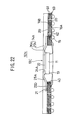
- Fig. 2 shows a semiconductor device 10A of a first embodiment of the present invention.
- the semiconductor device 10A comprises a semiconductor chip 11, a printed wiring board 12A, a heat spreader 13A, a sealing resin 14A, and solder balls 15.
- the semiconductor chip 11 is a high density and high power dissipation device. When operated, the semiconductor chip 11 generates a large amount of heat.
- the printed wiring board 12A is used as a wiring board.
- the printed wiring board 12A is a glass-epoxy resin substrate, and a wiring layer 16 is formed on the side of the wiring board 12A provided with the solder balls 15 (hereinafter referred to as a packaging side surface 28).
- the wiring layer 16 is made of copper (Cu), for instance, and its surface is protected by a resist 20.
- solder balls 15 which serve as external connecting terminals, are connected to the outer portion of the wiring layer 16 via holes 42 (shown in Fig. 10) formed through the resist 20. Bonding pads 17, to which wires 19 to be electrically connected to the semiconductor chip 11 are bonded, are formed on the inner portion of the wiring layer 16.
- a rectangular opening 40 is formed in the center of the printed wiring board 12A.
- the size of the opening 40 seen on a plane is larger than the size of the semiconductor chip 11 seen on a plane, so that the semiconductor chip 11 can be attached within the opening 40.
- the heat spreader 13A functions as a heat radiating plate, and therefore is made of a metallic material having excellent thermal conductivity, such as copper (Cu) or aluminum (Al).
- the heat spreader 13A is integrally made up of a fixed portion 23A, a stage portion 24A, and connecting portions 25A.
- Fig. 5 is a plan view of the heat spreader 13A.
- the heat spreader 13A shown in Fig. 5 is not yet integrated into the semiconductor device 10A (Fig. 5 is an enlarged view of the region circled by a broken line A in Fig. 4).
- the fixed portion 23A is fixed onto the upper surface 29 of the printed wiring board 12A.
- the upper surface 29 is the opposite surface to the packaging side surface 28, and provided with a plurality of anchor holes 33A.
- the fixed portion 23A extends to the outer periphery of the printed wiring board 12A, and the peripheral portion is exposed to the outside.
- a first adhesive 21 for temporarily fixing the heat spreader 13A to the printed wiring board 12A in a heat spreader temporary fixing process is disposed between the fixed portion 23A and the printed wiring board 12A.
- the stage portion 24A faces the opening 40 formed in the printed wiring board 12A, and is caved in the direction of an arrow Z shown in Fig. 2 with respect to the fixed portion 23A.
- the semiconductor chip 11 is mounted onto the stage portion 24A, and a concave portion 35 is formed in the position where the semiconductor chip 11 is to be disposed, as indicated by the shaded portion in Fig. 5.
- a second adhesive 22 is used in bonding the semiconductor chip 11 to the stage portion 24A.
- the second adhesive 22 contains metallic powder so as to have high thermal conductivity.
- the stage portion 24A and the semiconductor chip 11 are thermally bonded with the second adhesive 22.
- Other types of adhesive can be used as the second adhesive 22, as long as they have high thermal conductivity.
- the semiconductor chip mounting surface of the stage portion 24A is not flat.
- the second adhesive 22 fills in the uneven portions, so that a larger amount of adhesive assures the sealing between the stage portion 24A and the semiconductor chip 11.
- the concave portion 35 has a grid pattern, the design of the concave portion 35 is not limited to this. As long as the sealing between the stage portion 24A and the semiconductor chip 11 is surely maintained, the concave portion 35 can have other shapes, such as circles or triangles.
- the connecting portions 25A connect the fixed portion 23A and the stage portion 24A, and are situated between the fixed portion 23A and the four corners of the stage portion 24A. As shown in Fig. 2, the connecting portions 25A, the fixed portion 23A, and the stage portion 24A are at angles so that the stage portion 24A is caved in the direction of the arrow Z with respect to the fixed portion 23A. Furthermore, the inner rims of the fixed portion 23A conform to the rim of the opening 40. Because of this, the connecting portions 25A extend from the rim of the opening 40 formed in the printed wiring board 12A.
- a space (a cavity portion 41) is formed in the center of the semiconductor device 10A.
- the semiconductor chip 11 is disposed in the cavity portion 41.
- the sealing resin 14A is made up of a first sealing resin portion 26A and a second sealing resin portion 27A.
- the first sealing resin portion 26A and the second sealing resin portion 27A are integrally formed via resin filling openings 43A (shown in Fig. 5) formed on the sides of the connecting portions 25.
- the first sealing resin portion 26A is formed on the bonding side of the semiconductor chip 11 of the heat spreader 13A to protect the semiconductor chip 11 and the wires 19.
- the second sealing resin portion 27A is formed on the opposite surface to the bonding side of the semiconductor chip 11, and the stage portion 24A is exposed from the second sealing resin portion 27A.
- the second sealing resin portion 27A bonds the heat spreader 13A to the printed wiring board 12A.
- the solder balls 15 are used as the external connecting terminals, and are electrically connected to the wiring layer 16 via the holes 42 formed through the resist 20.
- the solder balls 15 can be formed on the entire surface of the packaging side surface 28 of the printed wiring board 12A (except the position of the opening 40), and can have grid patterns. Because of this, a large number of solder balls 15 can be arranged on the printed wiring board 12A while maintaining relatively wide intervals between the balls.
- the semiconductor chip 11 has high density, and is compatible with a large number of terminals.
- the semiconductor chip 11 is thermally bonded to the heat spreader 13A, and the stage portion 24A of the heat spreader 13A, to which stage portion 24A the semiconductor chip 11 is bonded, is exposed from the sealing resin (the second sealing resin portion 27A).
- the sealing resin the second sealing resin portion 27A
- the fixed portion 23A is exposed to the outside from the second sealing resin portion 27A so as to release the heat from this end also.
- the semiconductor chip 11 can be efficiently cooled down so as to surely avoid faulty operation of the semiconductor chip 11.
- the cavity portion 41 is formed in the position of the semiconductor chip 11.
- the semiconductor chip 11 With the semiconductor chip 11 being placed on the heat spreader 13A, a part of the semiconductor chip 11 is situated inside the printed wiring board 12A.
- the circuit formation surface (the surface to which the wires 19 are bonded) of the semiconductor chip 11 becomes level with the packaging side surface 28 of the printed wiring board 12A or slightly caved from the packaging side surface 28.
- the semiconductor device 10A can be thinner than the conventional semiconductor device 1 shown in Fig. 1 having the semiconductor chip 2 on the circuit board 3.
- the sealing resin 14A is made up of the first and second sealing resin portions 26A and 27A, which sandwich the heat spreader 13A. As a result, when subjected to heat, the first and second sealing resin portions 26A and 27A are heat-deformed in the same manner. Thus, the heat spreader 13A (the semiconductor device 10A) can be well prevented from being deformed, compared with a structure having the sealing resin 14A only on one surface of the heat spreader 13A.
- the inner rim of the fixed portion 23A conforms to the rim of the opening 40, so that the connecting portions 25A extend outward from the rim of the opening formed through the printed wiring board 12A.
- the bonding pads 17, to which the wires 19 are bonded, are formed around the outer periphery of the opening 40 of the printed wiring board 12A. Accordingly, the fixed portion 23A of the heat spreader 13A is always situated on the side of the printed wiring board 12A reverse to the positions of the bonding pads 17.
- the fixed portion 23A of the heat spreader 13A functions as a backing board at the time of wire bonding.
- the fixed portion 23A can accurately transmit ultrasonic vibration applied at the time of wire bonding to the wires 19 and the printed wiring board 12A, thereby maintaining good wire bonding workability.
- the connecting portions 25A extend outward from the rim of the opening 40, so that the rim of the opening 40 does not face the connecting portions 25A and the stage portion 24A of the heat spreader 13A.
- the printed wiring board 12A does not face the connecting portions 25A and the stage portion 24A.
- the printed wiring board 12A When wire-bonding the semiconductor chip 11 on the stage portion 24A, the printed wiring board 12A never hinders a capillary operation, thereby maintaining smooth wire bonding workability.
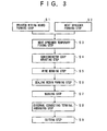
- Fig. 3 is a flowchart of the method of producing the semiconductor device 10A.
- the method of producing the semiconductor device 10A comprises a printed wiring board forming step (step 1: “step” will be hereinafter referred to as "S"), a heat spreader forming step (S2), a heat spreader temporary fixing step (S3), a semiconductor chip mounting step (S4), a wire bonding step (S5), a sealing resin forming step (S6), a marking step (S7), an external connecting terminal arranging step (S8), and a cutting step (S9).
- step 1 printed wiring board forming step
- S2 heat spreader forming step
- S3 heat spreader temporary fixing step
- S4 semiconductor chip mounting step
- S5 wire bonding step
- S6 sealing resin forming step
- S7 marking step
- S8 an external connecting terminal arranging step
- S9 a cutting step
- the printed wiring board forming step (S1) is a step of forming the printed wiring board 12A.
- the wiring layer 16 having junction electrodes 18 (shown in Fig. 8) to which the solder balls 15 are attached are formed on a glass-epoxy resin basic material by a plating method and an etching method.
- the opening 40 through which the semiconductor chip 11 is attached, is formed in the center of the wiring layer 16.
- the opening 40 is formed by stamping. The stamping can be carried out before or after the formation of the wiring layer 16.
- a so-called multi-cavity molding is performed to form a basic material into a plurality of printed wiring boards 12A. More specifically, twenty printed wiring boards 12A are formed from one basic material.
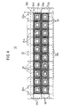
- Fig. 8 is a partially enlarged view of one of the printed wiring boards 12A formed in the printed wiring board forming step (S1). As shown in Fig. 8, the bonding pads 17 are arranged in a grid pattern, and gap portions 37 are formed at intervals in the bonding pad formation area.
- the area in which the bonding pads 17 are formed needs to be small.
- the bolding pads 17 are arranged in a grid pattern so as to make the bonding pad formation area small.
- the gap portions 37 are formed at intervals in the bonding pad formation area. The gap portions 37 reverse the wire bonding positions in the gap portions 37, thereby allowing more space of the wires 19. Thus, crossings of the wires 19 can be avoided.
- the heat spreader forming step (S2) is a step of forming the heat spreader 13A.
- stamping is carried out on a basic material, such as a copper plate or an aluminum plate having good thermal conductivity, to form the heat spreader 31A.
- Fig. 4 shows a heat spreader 13 formed in the heat spreader temporary fixing step. As shown in Fig. 4, multi-cavity molding is performed in this embodiment, and one heat spreader 13 includes twenty heat spreaders 13A.
- each thermal conducting plate disposed in the semiconductor device 10A is referred to as the heat spreader 13A, and thermal conducting plates connected to each other (as shown in Fig. 4) are referred to as the heat spreader 13.
- the twenty heat spreaders 13A are surrounded by outer periphery anchor holes 31A on the outer periphery of the heat spreader 13. Cutting slits are also formed in a grid pattern. Positioning holes 32A are also formed, and the stage portion 24A is formed in the center of each heat spreader 13A. The stage portion 24A is caved with respect to the fixed portion 23A.
- the outer periphery anchor holes 31A improve the bond between the sealing resin 14A and the heat spreader 13 in the sealing resin forming step (S6).
- the cutting slits 30 are formed along the cutting positions of a blade used in cutting the semiconductor device 10A in the cutting step (S9).
- the positioning holes 32A position the printed wiring board 12A with respect to the heat spreader 13, and metal molds 45 and 46 (shown in Fig. 11) with respect to the heat spreader 13, in the heat spreader temporary fixing step (S3) and the sealing resin forming step (S6).
- the outer periphery anchor holes 31A are circular on a plan view, and the cutting slits 30 are narrow rectangular on a plan view in this embodiment.
- the outer periphery anchor holes 31A and the cutting slits 30 may have other shapes.
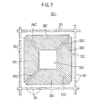
- Fig. 5 shows one of the heat spreaders 13A in the heat spreader 13.
- Each heat spreader 13A comprises the fixed portion 23A, the stage portion 24A, connecting portions 25A, cutting slits 30, anchor holes 33A, slits 34, and resin filling openings 43A.
- the fixed portion 23A, the stage portion 24A, the connecting portions 25A, the cutting slits 30, and the resin filling openings 43A have already been explained in the foregoing description.
- Each of the anchor holes 33A is circular on a plan view in this embodiment. Eighty of the anchor holes 33A are formed through the fixed portion 23A, surrounding the stage portion 24A.
- Each of the heat spreaders 13A is bonded to one printed wiring board 12A, and in the bonded condition, anchor grooves or anchor holes (not shown) of the printed wiring board 12A face the anchor holes 33A of he heat spreader 13A.
- the slits 34 are formed in the bonding positions between the fixed portion 23A and the connecting portions 25A.
- Each slit 34 is U-shaped, and 0.15 mm in width and 0.5 mm in length.
- the slits 34 formed in the stress applied positions become deformed to absorb the applied stress.
- unwanted deformation or distortion is not caused to the fixed portion 23A, the stage portion 24A, and the connecting portions 25A.
- the slits 34 are formed at the bonding positions between the connecting portions 25A and the fixed portion 23A in this embodiment, the slits 34 may be formed at the bonding positions between the stage portion 24a and the connecting portions 25A.
- Figs. 6 and 7 illustrate heat spreaders 13B and 13C which are modifications of the heat spreader 13A shown in Fig. 5.
- the heat spreader 13B of Fig. 6 is characterized by rectangular anchor holes 33B.
- the anchor holes 33A in the heat spreader 13A of Fig. 5 are circular, but the anchor holes 33A may have rectangular shapes as shown in Fig. 6 or other shapes.
- the heat spreader 13C of Fig. 7 has connecting portions 25C which are smaller in area.
- anchor holes 33C can also function as the resin filling openings. Accordingly, the anchor holes 33C can improve the bond with the printed wiring board 12A, and as the resin filling openings, the anchor holes 33C can improve the performance in filling the sealing resin 14A in the sealing resin forming step.
- the printed wiring board forming step (S1) and the heat spreader forming step (S2) can be carried out at the same time as separate steps.
- the order of the two steps is not particularly fixed.
- the printed wiring board forming step (S1) and the heat spreader forming step (S2) are followed by the heat spreader temporary fixing step (S3).
- the heat spreader 13 (13A) is temporarily fixed to the printed wiring board 12A.
- the stage portion 24A of the heat spreader 13A is positioned by the positioning openings 32 and others so as to face the opening 40 formed through the printed wiring board 12A.
- the heat spreader 13 (13A) is then temporarily fixed to the printed wiring board 12A.
- the first adhesive 21 is used in temporarily fixing the heat spreader 13 (13A) to the printed wiring board 12A.
- the heat spreader 13 (13A) and the printed wiring board 12A can be handled as a unit, and the workability in assembling the semiconductor device 10A is improved.
- the means for temporarily fixing the heat spreader is not limited to the adhesive 21. It is also possible to perform laser welding as shown in Fig. 9. When the heat spreader 13 (13A) is temporarily fixed to the printed wiring board 12A by laser welding, a dummy pattern should be formed in advance in a position where no bonding pads 17 of the printed wiring board 12A exist.
- a laser welding device is used to weld the fixed portion 23A of the heat spreader 13 (13A) to the dummy pattern 38 on the printed wiring board 12A.
- the heat spreader 13 (13A) can be bonded to the printed wiring board 12A by laser welding.
- bonding can be carried out in positions which require a particularly tight bond. Even if the wiring density on the printed wiring board 12A is high (in a case where wiring is carried out on the upper surface 29 of the printed wiring board 12A), the printed wiring board 12A and the heat spreader 13 (13A) can be tightly bonded.
- the heat spreader 13 (13A) and the printed wiring board 12A can be permanently bonded by welding.
- the welding means described above is not limited to laser welding, but other welding means (such as spot welding) can be used.
- the heat spreader temporary fixing step (S3) is followed by the semiconductor chip mounting step (S4) and the wire bonding step (S5) in that order.
- Fig. 10 illustrates the conditions after the semiconductor chip mounting step (S4) and the wire bonding step (S5).
- the semiconductor mounting step (S4) and the wire bonding step (S5) are followed by the sealing resin forming step (S6).
- the sealing resin forming step the sealing resin 14A (i.e., the first sealing resin portion 26A and the second sealing resin portion 27A) is formed.
- the sealing resin 14A is formed by a transfer molding method, for instance.
- Figs. 11A and 11B illustrate a metal mold for forming the sealing resin 14A.
- the heat spreader 13 having the semiconductor chip 11 and the printed wiring board 12A are inserted in the metal mold so as to form the sealing resin 14A.
- Fig. 11A illustrates an upper mold 45
- Fig. 11B illustrates a lower mold 46.
- the upper mold 45 is provided with upper cavities 47 and positioning holes 48.
- the upper cavities 47 face the semiconductor chip 11 when the heat spreader 13 and the printed wiring board 12A are attached to the upper mold 45.
- the upper cavities 47 are mainly used for forming the first sealing resin portion 26A.
- the lower mold 46 is provided with a lower cavity 49, a runner 50 for filling resin, gates 51, area vents 52, and positioning pins 53 for positioning the upper mold 45.
- the lower cavity 49 is mainly used for forming the second sealing resin portion 27A, which is provided to the twenty heat spreaders 13A at once.
- the lower mold 46 has a number of gates 51 formed on the runner 50, so that resin filling can be smoothly carried out even if the lower cavity 49 is large in area (or volume).
- the resin injected from an injection molding machine (not shown) is filled in the runner 50 in the direction indicated by the arrow in Fig. 11B, and the resin enters from the gates 50 into the lower cavity 49. Since each heat spreader 13A is provided with the resin filling openings 43A (shown in Fig. 5), the resin in the lower cavity 49 then enters the upper cavities 47 of the upper mold 45 through the resin filling openings 43A. Thus, the first and second sealing resin portions 26A and 27 are formed simultaneously in the sealing resin forming step.
- the large-area second sealing portion 27A is collectively formed on the entire surface of the heat spreader 13 (except in the position of the stage portion 24A) in the sealing resin forming step, so that large-area molding can be carried out.
- the production efficiency is high, compared with the conventional structure in which the heat spreaders 13A and the printed wiring board 12A are divided in advance, and the sealing resin is formed individually. In this embodiment, the production costs can also be reduced.
- the heat spreaders 13A and the printed wiring board 12A are collectively formed. This also improves the production efficiency and reduces the production costs.
- Figs. 12 and 13 illustrate the heat spreader 13 and the printed wiring board 12A after the sealing resin forming step.
- Fig. 12 is a view from the heat spreader 13 side
- Fig. 13 is a view from the printed wiring board 12A side.
- the second sealing resin portion 27A is filled in the anchor holes 33 formed in the fixed portion 34A of each heat spreader 13A, and in the anchor grooves (or the anchor holes) in the printed wiring board 12A.
- the anchor grooves face the anchor holes 33A.
- the resin is also filled in the outer periphery anchor holes 31A (shown in Fig. 4) formed on the outer periphery of the heat spreader 13.
- the sealing resin 14A also functions as a fixing member for fixing the heat spreader 13 onto the printed wiring board 12A.
- the sealing resin forming step (S6) After the sealing resin forming step (S6), the heat spreader 13 and the printed wiring board 12A provided with the sealing resin 14A are separated from the metal mold (45 and 46).
- the marking step (S7) is then carried out for putting a mark for identifying the semiconductor device 10A in a predetermined position in the sealing resin 14A.
- the marking step is followed by the external connecting terminal arranging step (S8) carried out for arranging the solder balls 15.
- the solder balls 15 are arranged on the printed wiring board 12A by a transferring method, for instance.
- the external connecting terminal arranging step (S8) is followed by the cutting step (S9).
- the heat spreader 13, the printed wiring board 12A, and the sealing resin 14A are collectively cut with a blade at the outer periphery of a corresponding semiconductor device 10A.
- the semiconductor device 10A shown in Fig. 2 can be obtained.
- the heat spreader 13 is provided with the cutting slits 30 formed along the cutting line of the blade.
- the cutting slits 30 are formed even on the outer periphery of the heat spreader 13. In this manner, a load applied to the blade is reduced, and the life of the blade is prolonged.
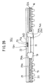
- Fig. 14 illustrates a semiconductor device 10B of a second embodiment of the present invention.
- the same components as in the first embodiment are indicated by the same reference numerals as in the semiconductor device 10A shown in Fig. 2.
- the printed wiring board 12A is used as a wiring board.
- a film-type board 55 having a tape material as a base material is used as the wiring board.
- the base material of the film-type board 55 is polyimide, and the wiring layer 16 is copper foil as in the printed wiring board 12A.
- the film-type board 55 can improve the wiring density, because the wiring layer 16 can be made more minute compared with the printed wiring board 12A.
- the film-type board 55 used as the wiring board is compatible with the high-density semiconductor chip 11.
- the semiconductor device 10B can be made thinner than the semiconductor device 10A.
- the relationship between each line and space can be 30/30 pm.
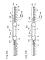
- Figs. 15A and 15B illustrate semiconductor devices 10C and 10D of third and fourth embodiments of the present invention.
- the semiconductor device 10C of the third embodiment shown in Fig. 15A has a first resist 20A formed on the packaging side surface 28 of the printed wiring board 12A and a second resist 20B formed on the upper surface 29 opposite to the packaging side surface 28.
- the first and second resists 20A and 20B function as solder resists, and are made of a resin material.
- the first and second resin resists 20A and 20B sandwich the printed wiring board 12A, so that the first and second resin resists 20A and 20B are deformed in the same way when heat is applied.
- the printed wiring board 12A (or the semiconductor device 10C) is thus prevented from bending.
- the semiconductor device 10D of the fourth embodiment shown in Fig. 15B has the film-type board 55 instead of the printed wiring board 12A in the semiconductor device 10C of the third embodiment shown in Fig. 15A.
- the length of a fixed portion 23D of a heat spreader 13C is shorter than that of the semiconductor device 10A or 10B. As long as the bonding between the heat spreader 13C and the printed wiring board 12A is maintained, the fixed portion 23D can be shorter. This can reduce the material cost.
- Figs. 16A and 16B illustrate semiconductor devices 10E and 10F of fifth and sixth embodiments of the present invention.
- the semiconductor device 10E of the fifth embodiment shown in Fig. 16A has an elastic portion 56 at each connecting portion 25D connecting the stage portion 24A and the fixed portion 23D formed in a heat spreader 13D.
- each connecting portion 25D is crimped to form the elastic portion 56.
- the stage portion 24A can be shifted with respect to the fixed portion 23D. Even if the semiconductor chip 11 and the printed wiring board 12A change in thickness, resin molding can be carried out using the same metal mold (45 and 46) used for forming the sealing resin 14A.
- the semiconductor chip 11 and the printed wiring board 12A might change in thickness depending on the structure of the semiconductor device.
- the connecting portions are inelastic like the connecting portions 25A of the first embodiment, the heat spreader 13 needs to be adjusted to the thicknesses of the semiconductor chip and the printed wiring board 12A. Because of this, it also becomes necessary to form the metal mold for the sealing resin 14A in accordance with the adjustment. As is well known, the cost for producing a metal mold is high, resulting in an increase of the production costs of the semiconductor device.
- the elastic portion 56 at each connecting portion 25 of the present invention is designed to absorb a change in thickness of the semiconductor chip 11 or the printed wiring board 12A.
- the sealing resin 14A can be formed, without changing or adjusting the metal molds. Accordingly, a change in the semiconductor chip 11 or the printed wiring board 12A can be quickly accommodated, without causing an increase of the production costs of the semiconductor device 10E.
- the semiconductor device 10F of the sixth embodiment shown in Fig. 16B has the film-type board 55 instead of the printed wiring board 12A in the semiconductor device 10E of the fifth embodiment shown in Fig. 16A.
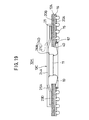
- Figs. 17A and 17B illustrate semiconductor devices 10G and 10H of seventh and eighth embodiments of the present invention.
- the semiconductor device 10G of the seventh embodiment shown in Fig. 17A is characterized by the stage portion 24A protruding from the surface of a second sealing resin portion 27B.
- the stage portion 24A protrudes by the length indicated by arrows H1 in Fig. 17A.
- the stage portion 24A protruding from the surface of the second sealing resin portion 27B can be easily obtained by forming a cavity for accommodating the stage portion 24A in the lower cavity 49 (shown in Fig. 11B) of the lower mold 46 used in the sealing resin forming step (S6).
- the stage portion 24A protruding from the surface of the second sealing resin portion 27B of this embodiment has a larger area exposed from the second sealing resin portion 27B than in the foregoing embodiments, and the exposed area is the heat releasing area.
- the heat generated from the semiconductor chip 11 can be more efficiently released.
- the semiconductor device 10H of the eighth embodiment shown in Fig. 17B has the film-type board 55 instead of the printed wiring board 12A in the semiconductor device 10G of the seventh embodiment shown in Fig. 17A.
- Figs. 18A and 18B illustrate semiconductor devices 10I and 10J of ninth and tenth embodiments of the present invention.
- the semiconductor device 10I of the ninth embodiment shown in Fig. 18A is characterized by a second sealing resin portion 27C having a smaller area than the printed wiring board 12A.
- the upper surface 29 of the printed wiring board 12A is exposed, and the second resist 20B is formed on the upper surface 29 to protect the printed wiring board 12.
- the first sealing resin portion 26A and the second sealing resin portion 27C can be similar in area. If heating is performed at the time of packaging, the thermal expansion of the first sealing resin portion 26A can be almost the same as the thermal expansion of the second sealing resin portion 27C. Thus, the heat spreader 13C can be prevented from being bent due to the heat.
- the semiconductor device 10J of the tenth embodiment shown in Fig. 18B has the film-type board 55 instead of the printed wiring board 12A in the semiconductor device 10I of the ninth embodiment shown in Fig. 18A.
- Fig. 19 illustrates a semiconductor device 10K of an eleventh embodiment of the present invention.
- the semiconductor device 10K of this embodiment has a first sealing resin portion 26B formed by a screen printing method.
- a dam member 57 for preventing resin flow at the time of printing is formed near the opening 40 of the printed wiring board 12A.
- the resin filling pressure can be lower than the pressure caused in resin formation by the transfer molding method.
- the wires 19 can be prevented from moving at the time of resin formation. If the wire pitch of the wires 19 becomes narrow due to a high density, a short circuit among the wires can be avoided.
- the screen printing method can also reduce the equipment cost, thereby reducing the costs of the semiconductor device 10K.
- the first sealing resin portion 26B and the second sealing resin portion 27C need to be produced separately. More specifically, the first sealing resin portion 26B is formed by the screen printing method, and cured. After the curing, the second sealing resin portion 27C is formed by the transfer molding method.
- the film-type board 55 can be employed in place of the printed wiring board 12A.
- Fig. 20 illustrates a semiconductor device 10L of a twelfth embodiment of the present invention.
- the semiconductor device 10L of this embodiment has an inorganic material board 60 as a wiring board made of an inorganic material such as ceramic (hereinafter referred to as a ceramic wiring board).
- the ceramic wiring board 60 of this embodiment can have a higher wire density, and is compatible with a high density semiconductor chip 11. As the ceramic wiring board 60 does not absorb moisture, cracking due to vapor can be avoided at the time of heating. Thus, the semiconductor device 10L can have high reliability.
- Figs. 21 and 22 illustrate semiconductor devices 10M and 10N of thirteenth and fourteenth embodiments of the present invention.
- the semiconductor device 10M of the thirteenth embodiment shown in Fig. 21 has a first wiring layer 16A formed on the packaging side surface 18 of a printed wiring board 12C, and a second wiring layer 16B formed on the upper surface 29 of the printed wiring board 12C opposite to the packaging side surface 28.
- the semiconductor device 10N of the fourteenth embodiment shown in Fig. 22 has a multilayer printed wiring board 63 having a laminated structure as a wiring board.
- the multi layer printed wiring board 63 of this embodiment is provided with the first and second wiring layers 16A and 16B on opposite surfaces.
- the semiconductor devices 10M and 10N both have the first and second wiring layers 16A and 16B on opposite surfaces of the printed wiring board 12C and the multi layer printed wiring board 63 as the circuit boards, an internal wiring layer 61 and vias 62 for electrically connecting the wiring layers 16A and 16B are formed inside each of the wiring boards 12C and 63.
- the semiconductor device 10M of the thirteenth embodiment is provided with the second wiring layer 16B on the upper surface 29.
- the semiconductor device 10N employs the multi layer printed wiring board 63 having a laminated structure. These factors can improve the degree of freedom and also narrow the gaps in the wiring pattern. Thus, the high density semiconductor chip 11 can be accommodated.
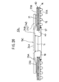
- Figs. 23 and 24 illustrate semiconductor devices 10P and 10Q of fifteenth and sixteenth embodiments of the present invention.
- the semiconductor device 10P of the fifteenth embodiment shown in Fig. 23 has an anchor portion 64 wedged into the printed wiring board 12A.
- the anchor portion 64 is integrally formed with the fixed portion 23D of a heat spreader 13E in the heat spreader forming step (S2).
- the anchor portion 64 is long enough to fix the heat spreader 13E to the printed wiring board 12A.
- the semiconductor device 10Q of the sixteenth embodiment shown in Fig. 24 has an engaging portion 65 extending downward from a heat spreader 13F.
- the engaging portion 65 is engaged with the opening 40.
- the anchor portion 64 provided to the heat spreader 13E and the engaging portion 65 provided to the heat spreader 13F can mechanically fix both heat spreaders 13E and 13F to the respective printed wiring boards 12A.
- Fig. 25 illustrates a semiconductor device 10R of a seventeenth embodiment of the present invention.
- the semiconductor device 10R of this embodiment has a protruding portion 66 integrally formed with a first sealing resin portion 26C.
- the protruding portion 66 protrudes in the same direction as the protruding direction of the solder balls 15.
- the protruding portion 66 is more protruding than the packaging side surface 28 of the printed wiring board 12A, but the solder balls 15 are more protruding than the protruding portion 66 by the length indicated by arrows H2 in Fig. 25.
- the protruding portion 66 provided to the first sealing resin portion 26C can prevent the semiconductor device 10R from shifting at the time of packaging.
- the semiconductor device 10R is mounted to a packaging substrate (not shown)
- the semiconductor device 10R is supported by the solder balls 15 onto the packaging substrate prior to the melting of the solder balls 15. After heat is applied for the packaging, the melted solder balls 15 can no longer support the semiconductor device 10R.
- the printed wiring board 12A shifts toward the packaging substrate due to the weight of the semiconductor device 10R itself. This causes bridging between the melted solder balls 15.
- the semiconductor device 10R floats on the melted solder balls 15, and can be deviated by even a small external force.
- the protruding portion 66 protruding from the printed wiring board 12A can support the semiconductor device 10R on the packaging substrate even after the melting of the solder balls 15. Thus, bridging between the melted solder balls 15 can be avoided, and the semiconductor device 10R can be prevented from deviating on the packaging substrate.
- the height of the protruding portion 66 is smaller than the height of the solder balls 15, so that the protruding portion 66 is not brought into contact with the packaging substrate.
- Figs. 26 and 27 illustrate semiconductor devices 10S and 10T of eighteenth and nineteenth embodiments of the present invention.
- the semiconductor device 10S of the eighteenth embodiment shown in Fig. 26 has a thin portion 67 on the outer periphery of a fixed portion 23E of a heat spreader 13G.
- the outer periphery of the heat spreader 13G is where the blade cutting is carried out in the cutting step (S9).
- the thin portion 67 is formed in the blade cutting position. As for the process of forming the thin portion 67, it is possible to form the thin portion 67 at the same time as forming the cutting slits 30 by stamping in the heat spreader forming step (S2), for instance.
- the thin portion 67 formed on the outer periphery of the heat spreader 13G, where the cutting step is carried out, can reduce the load applied to the blade used for the cutting.
- a second sealing resin portion 27D enters the thin portion 67 to form an anchor portion 68, so that the bond between the second sealing resin portion 27D and the heat spreader 13G can be improved.
- the semiconductor device 10T of the nineteenth embodiment shown in Fig. 27 has a base thin portion 69 on the outer periphery of a printed wiring board 12D.
- the base thin portion 69 formed on the outer periphery of the printed wiring board 12D, where the cutting step is carried out, can reduce the load applied to the blade used for the cutting, as in the eighteenth embodiment.
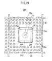
- Figs. 28 and 29 illustrate a semiconductor device 10U of a twentieth embodiment of the present invention.
- Fig. 28 is a sectional view of the semiconductor device 10U of this embodiment
- Fig. 29 is an enlarged plan view of a heat spreader 13H disposed in the semiconductor device 10U.
- the semiconductor device 10U has a vent hole 70 for releasing vapor from inside the device at the time of packaging.
- the vent hole 70 is formed in a stage portion 24D provided to the heat spreader 13H. As shown in Fig. 29, the vent hole 70 is formed in the center of the stage portion 24D, and has a circular shape. However, the position of the vent hole 70 is not limited to the center of the stage portion 24D, and the number and shape of the vent hole 70 can be different from those in this embodiment.
- the vent hole 70 formed in the stage portion 24D exposed from the sealing resin 14A (or the first sealing resin portion 26A) can release vapor caused by the heat applied at the time of packaging. Accordingly, when heating is carried out, the semiconductor device 10U can be prevented from sustaining damage such as cracks, and the reliability of the semiconductor device 10U can be improved.
- the second adhesive 22 leaks from the vent hole 70 formed in the stage portion 24D.
- a tape member 71A for blocking the vent hole 70 is attached to the surface on the semiconductor chip mounting side of the stage 24D in this embodiment.
- the tape member 71A for blocking the vent hole 70 can prevent the second adhesive 22 from leaking from the vent hole 70 in the semiconductor chip mounting step (S4), thereby assuring the mounting of the semiconductor chip 11 to the stage portion 24D.
- the tape member 71A of this embodiment is holed prior to the heating of the semiconductor device 10U.
- the vent hole 70 is subjected to laser irradiation, or a jig is inserted into the vent hole 70.
- a tape having high heat resistance such as Kapton
- Kapton can be used as the tape member 71A of this embodiment.
- the tape member 71A is not limited to Kapton, and other materials can be employed as long as they have strong adhesion and heat resistance.
- Fig. 30 illustrates a semiconductor device 10V of a twenty-first embodiment of the present invention.
- the semiconductor device 10V of this embodiment has the vent hole 70 for releasing vapor at the time of heating, as in the semiconductor device 10U of the twentieth embodiment.
- the tape member 71A for preventing the second adhesive 22 from leaking is attached to the semiconductor chip mounting surface of the stage portion 24D in the twentieth embodiment
- a tape member 71B is attached to the outer exposed surface of the stage portion 24D in this embodiment.
- the tape member 71B of this embodiment can be removed from the outside of the semiconductor device 10V. Compared with the twentieth embodiment, removing the tape member 71B is easier.
- a UV tape which loses adhesion by ultraviolet rays can be used as the tape member 71B.
- Fig. 31 illustrates a semiconductor device 10W of a twenty-second embodiment of the present invention.
- the semiconductor device 10W of the twenty-second embodiment has a plating portion 72 having corrosion resistance on the exposed surface of the stage portion 24A.
- the heat spreader 13A If copper (Cu) is used for the heat spreader 13A, and epoxy resin is used for the sealing resin 14A, it is advantageous to bond the heat spreader 13A and the sealing resin 14A without plating, because both copper and epoxy have excellent bonding properties. However, copper easily discolors or corrodes when exposed to the air. In the semiconductor device 10W having the stage portion 24A exposed from the first sealing resin portion 26A, the stage portion 24A made of copper discolors or corrodes, and lowers the quality of the device.
- the plating portion 72 is formed only in the stage portion 24a exposed to the outside.
- the plating portion 72 prevents the stage portion 24A from discoloring and corroding while maintaining the bond between the heat spreader 13A and the sealing resin 14A.
- the quality of the semiconductor device 10W can be maintained for a long period of time.
Abstract
Description
- The present invention generally relates to a semiconductor device and a method of producing the semiconductor device. More particularly, the present invention relates to a semiconductor device suitable for mounting a semiconductor chip which generates heat during an operation and to a method producing such a semiconductor device.
- As the density of a semiconductor chip has increased in recent years, the number of terminals in a semiconductor chip has increased accordingly. Also, there is a growing tendency for a semiconductor chip to consume a large amount of electric power and to generate a large amount of heat.
- In the meantime, electric devices mounted with semiconductor chips have rapidly become smaller, and there is a demand for smaller semiconductor chips. Therefore, it is necessary to develop a semiconductor chip which is small and thin, even if the number of terminals is large.
- Fig. 1 illustrates a conventional fine-pitch
type semiconductor device 1. Thissemiconductor device 1 has a package structure called FBGA (Fine-pitch Ball Grid Array). This structure includes asemiconductor chip 2, awiring board 3,solder balls 7, and asealing resin 8. - The
semiconductor chip 2 has a high density, and is fixed with anadhesive 5 onto the upper surface of thewiring board 3, which functions as an interposer. Thewiring board 3 is a printed wiring board or a flexible printed board (in Fig. 1, a flexible printed board is shown). Thewiring board 3 has awiring layer 4 formed on a polyimide tape. Thewiring layer 4 and thesemiconductor chip 2 are electrically connected by awire 6. - An opening is formed in a predetermined position of the polyimide tape, and the
solder balls 7 are bonded to thewiring layer 4 through the opening. Thus, thesemiconductor chip 2 is electrically connected to thesolder balls 7 as external connecting terminals via thewiring layer 4. - The sealing
resin 8 is molded to cover the semiconductor chip mounting surface of thewiring board 3, so as to protect thesemiconductor chip 2, thewiring layer 4, and thewire 6. - In the
semiconductor device 1 shown in Fig. 1, a fine pitch is obtained by arranging thesolder balls 7 in a grid pattern on thewiring board 3, so that thesemiconductor device 1 is compatible with the large number of terminals. - As a semiconductor chip has a higher density, the semiconductor chip generates a larger amount of heat. In the
semiconductor device 1, the only heat releasing passage for the heat generated from thesemiconductor chip 2 is thesealing resin 8 or thewiring board 3. However, the resin material used for the sealingresin 8 and thewiring board 3 is poor in thermal conductivity. The heat releasing efficiency of thesemiconductor device 1 is low, and the heat generated from thesemiconductor chip 2 stays inside the device. As a result, thesemiconductor chip 2 is overheated, and causes a faulty operation. - The principal object of the present invention is to provide a semiconductor device and a method of producing the semiconductor device, which semiconductor device is smaller than a conventional semiconductor device while maintaining high heat spreading properties.
- The object of the present invention is achieved by a semiconductor device including a semiconductor chip, a heat spreading plate, a wiring board, and a sealing resin. The semiconductor chip is mounted on the heat spreading plate having a stage portion. The sealing resin seals the semiconductor chip and the heat spreading plate so that the stage portion is exposed from the sealing resin.
- In this structure, heat generated from the semiconductor chip can be efficiently released through the stage portion to the outside, so that the semiconductor chip can be efficiently cooled to avoid faulty operations.
- The object of the present invention is also achieved by a method of producing a semiconductor device which includes the following steps of: forming a wiring board having a first wiring layer and an opening portion; forming a heat spreading plate having a fixed portion and a stage portion; temporarily fixing the heat spreading plate to the wiring board so that the stage portion facing the opening portion; mounting a semiconductor chip onto the stage portion; forming a sealing resin for permanently fixing the heat spreading plate to the wiring board so that the stage portion is exposed from the sealing resin; and cutting collectively the heat spreading plate, the wiring board, and the sealing resin, to form individual semiconductor devices.
- By this method, the heat spreading plate formed in the heat spreading plate forming step is temporarily fixed to the wiring board formed in the wiring board forming step, so that the heat spreading plate and the wiring board can be collectively assembled. In this manner, the workability is improved compared with a method in which the heat spreading plate and the wiring board are handled and assembled separately.
- The above and other objects and features of the present invention will become more apparent from the following description taken in conjunction with the accompanying drawings.
-
- Fig. 1 illustrates one example of a conventional semiconductor device;
- Fig. 2 illustrates a first embodiment of a semiconductor device of the present invention;
- Fig. 3 is a flowchart of a method of producing the semiconductor device of the first embodiment;
- Fig. 4 illustrates the semiconductor device of the first embodiment in a heat spreader forming step;
- Fig. 5 illustrates the semiconductor device of the first embodiment in the heat spreader forming step;
- Fig. 6 illustrates the semiconductor device of the first embodiment in the heat spreader forming step;
- Fig. 7 illustrates the semiconductor device of the first embodiment in the heat spreader forming step;
- Fig. 8 illustrates the semiconductor device of the first embodiment in a printed wiring board forming step;
- Fig. 9 illustrates the semiconductor device of the first embodiment in a heat spreader temporary fixing step;
- Fig. 10 illustrates the semiconductor device of the first embodiment in a semiconductor chip mounting step and a wire bonding step;
- Figs. 11A and 11B illustrate the semiconductor device of the first embodiment in a sealing resin forming step;
- Fig. 12 illustrates the semiconductor device of the first embodiment in the sealing resin forming step;
- Fig. 13 illustrates the semiconductor device of the first embodiment in the sealing resin forming step;
- Fig. 14 illustrates a second embodiment of the semiconductor device of the present invention;
- Figs. 15A and 15B illustrate third and fourth embodiments of the semiconductor device of the present invention;
- Figs. 16A and 16B illustrate fifth and sixth embodiments of the semiconductor device of the present invention;
- Figs. 17A and 17B illustrate seventh and eighth embodiments of the semiconductor device of the present invention;
- Figs. 18A and 18B illustrate ninth and tenth embodiments of the semiconductor device of the present invention;
- Fig. 19 illustrates an eleventh embodiment of the semiconductor device of the present invention;
- Fig. 20 illustrates a twelfth embodiment of the semiconductor device of the present invention;
- Fig. 21 illustrates a thirteenth embodiment of the semiconductor device of the present invention;
- Fig. 22 illustrates a fourteenth embodiment of the semiconductor device of the present invention;
- Fig. 23 illustrates a fifteenth embodiment of the semiconductor device of the present invention;
- Fig. 24 illustrates a sixteenth embodiment of the semiconductor device of the present invention;
- Fig. 25 illustrates a seventeenth embodiment of the semiconductor device of the present invention;
- Fig. 26 illustrates an eighteenth embodiment of the semiconductor device of the present invention;
- Fig. 27 illustrates a nineteenth embodiment of the semiconductor device of the present invention;
- Fig. 28 illustrates a twentieth embodiment of the semiconductor device of the present invention;
- Fig. 29 is an enlarged view of a heat spreader in the semiconductor device of the twentieth embodiment;
- Fig. 30 illustrates a twenty-first embodiment of the semiconductor device of the present invention; and
- Fig. 31 illustrates a twenty-second embodiment of the semiconductor device of the present invention.
-
- The following is a description of the embodiments of the present invention, with reference to the accompanying drawings.
- Fig. 2 shows a
semiconductor device 10A of a first embodiment of the present invention. Thesemiconductor device 10A comprises asemiconductor chip 11, a printedwiring board 12A, aheat spreader 13A, a sealingresin 14A, andsolder balls 15. - The
semiconductor chip 11 is a high density and high power dissipation device. When operated, thesemiconductor chip 11 generates a large amount of heat. - In this embodiment, the printed
wiring board 12A is used as a wiring board. The printedwiring board 12A is a glass-epoxy resin substrate, and awiring layer 16 is formed on the side of thewiring board 12A provided with the solder balls 15 (hereinafter referred to as a packaging side surface 28). Thewiring layer 16 is made of copper (Cu), for instance, and its surface is protected by a resist 20. - The
solder balls 15, which serve as external connecting terminals, are connected to the outer portion of thewiring layer 16 via holes 42 (shown in Fig. 10) formed through the resist 20.Bonding pads 17, to whichwires 19 to be electrically connected to thesemiconductor chip 11 are bonded, are formed on the inner portion of thewiring layer 16. - A
rectangular opening 40 is formed in the center of the printedwiring board 12A. The size of theopening 40 seen on a plane is larger than the size of thesemiconductor chip 11 seen on a plane, so that thesemiconductor chip 11 can be attached within theopening 40. - The
heat spreader 13A functions as a heat radiating plate, and therefore is made of a metallic material having excellent thermal conductivity, such as copper (Cu) or aluminum (Al). Theheat spreader 13A is integrally made up of a fixedportion 23A, astage portion 24A, and connectingportions 25A. - Fig. 5 is a plan view of the
heat spreader 13A. For ease of explanation, theheat spreader 13A shown in Fig. 5 is not yet integrated into thesemiconductor device 10A (Fig. 5 is an enlarged view of the region circled by a broken line A in Fig. 4). - The fixed
portion 23A is fixed onto theupper surface 29 of the printedwiring board 12A. Theupper surface 29 is the opposite surface to thepackaging side surface 28, and provided with a plurality ofanchor holes 33A. In this embodiment, the fixedportion 23A extends to the outer periphery of the printedwiring board 12A, and the peripheral portion is exposed to the outside. - A
first adhesive 21 for temporarily fixing theheat spreader 13A to the printedwiring board 12A in a heat spreader temporary fixing process (shown in Fig. 3) is disposed between the fixedportion 23A and the printedwiring board 12A. - The
stage portion 24A faces theopening 40 formed in the printedwiring board 12A, and is caved in the direction of an arrow Z shown in Fig. 2 with respect to the fixedportion 23A. Thesemiconductor chip 11 is mounted onto thestage portion 24A, and aconcave portion 35 is formed in the position where thesemiconductor chip 11 is to be disposed, as indicated by the shaded portion in Fig. 5. - A
second adhesive 22 is used in bonding thesemiconductor chip 11 to thestage portion 24A. The second adhesive 22 contains metallic powder so as to have high thermal conductivity. Thestage portion 24A and thesemiconductor chip 11 are thermally bonded with thesecond adhesive 22. Other types of adhesive can be used as thesecond adhesive 22, as long as they have high thermal conductivity. - With the
concave portion 35, the semiconductor chip mounting surface of thestage portion 24A is not flat. When bonding thesemiconductor chip 11 to thestage portion 24A, thesecond adhesive 22 fills in the uneven portions, so that a larger amount of adhesive assures the sealing between thestage portion 24A and thesemiconductor chip 11. - Although the
concave portion 35 has a grid pattern, the design of theconcave portion 35 is not limited to this. As long as the sealing between thestage portion 24A and thesemiconductor chip 11 is surely maintained, theconcave portion 35 can have other shapes, such as circles or triangles. - The connecting
portions 25A connect the fixedportion 23A and thestage portion 24A, and are situated between the fixedportion 23A and the four corners of thestage portion 24A. As shown in Fig. 2, the connectingportions 25A, the fixedportion 23A, and thestage portion 24A are at angles so that thestage portion 24A is caved in the direction of the arrow Z with respect to the fixedportion 23A. Furthermore, the inner rims of the fixedportion 23A conform to the rim of theopening 40. Because of this, the connectingportions 25A extend from the rim of theopening 40 formed in the printedwiring board 12A. - By caving the
stage portion 24A in the direction of the arrow Z with respect to the fixedportion 23A and forming theopening 40 in a position facing thestage portion 24A of the printedwiring board 12A, a space (a cavity portion 41) is formed in the center of thesemiconductor device 10A. Thesemiconductor chip 11 is disposed in thecavity portion 41. - The sealing
resin 14A is made up of a firstsealing resin portion 26A and a secondsealing resin portion 27A. The firstsealing resin portion 26A and the secondsealing resin portion 27A are integrally formed viaresin filling openings 43A (shown in Fig. 5) formed on the sides of the connecting portions 25. - The first
sealing resin portion 26A is formed on the bonding side of thesemiconductor chip 11 of theheat spreader 13A to protect thesemiconductor chip 11 and thewires 19. The secondsealing resin portion 27A is formed on the opposite surface to the bonding side of thesemiconductor chip 11, and thestage portion 24A is exposed from the secondsealing resin portion 27A. The secondsealing resin portion 27A bonds theheat spreader 13A to the printedwiring board 12A. - In this embodiment, the
solder balls 15 are used as the external connecting terminals, and are electrically connected to thewiring layer 16 via theholes 42 formed through the resist 20. Thesolder balls 15 can be formed on the entire surface of thepackaging side surface 28 of the printedwiring board 12A (except the position of the opening 40), and can have grid patterns. Because of this, a large number ofsolder balls 15 can be arranged on the printedwiring board 12A while maintaining relatively wide intervals between the balls. Thus, thesemiconductor chip 11 has high density, and is compatible with a large number of terminals. - In the
semiconductor device 10A having the above structure, thesemiconductor chip 11 is thermally bonded to theheat spreader 13A, and thestage portion 24A of theheat spreader 13A, to whichstage portion 24A thesemiconductor chip 11 is bonded, is exposed from the sealing resin (the secondsealing resin portion 27A). With this structure, heat generated from thesemiconductor chip 11 is efficiently released from thestage portion 24A to the outside. - In this embodiment, the fixed
portion 23A is exposed to the outside from the secondsealing resin portion 27A so as to release the heat from this end also. By doing so, thesemiconductor chip 11 can be efficiently cooled down so as to surely avoid faulty operation of thesemiconductor chip 11. - With the
stage portion 24A being caved in the direction of the arrow Z with respect to the fixedportion 23A and theopening 40 being formed through the printedwiring board 12A, thecavity portion 41 is formed in the position of thesemiconductor chip 11. With thesemiconductor chip 11 being placed on theheat spreader 13A, a part of thesemiconductor chip 11 is situated inside the printedwiring board 12A. - More specifically, in this embodiment, the circuit formation surface (the surface to which the
wires 19 are bonded) of thesemiconductor chip 11 becomes level with thepackaging side surface 28 of the printedwiring board 12A or slightly caved from thepackaging side surface 28. Thus, thesemiconductor device 10A can be thinner than theconventional semiconductor device 1 shown in Fig. 1 having thesemiconductor chip 2 on thecircuit board 3. - The sealing
resin 14A is made up of the first and second sealingresin portions heat spreader 13A. As a result, when subjected to heat, the first and second sealingresin portions heat spreader 13A (thesemiconductor device 10A) can be well prevented from being deformed, compared with a structure having the sealingresin 14A only on one surface of theheat spreader 13A. - As described above, the inner rim of the fixed
portion 23A conforms to the rim of theopening 40, so that the connectingportions 25A extend outward from the rim of the opening formed through the printedwiring board 12A. Thebonding pads 17, to which thewires 19 are bonded, are formed around the outer periphery of theopening 40 of the printedwiring board 12A. Accordingly, the fixedportion 23A of theheat spreader 13A is always situated on the side of the printedwiring board 12A reverse to the positions of thebonding pads 17. - The fixed
portion 23A of theheat spreader 13A functions as a backing board at the time of wire bonding. The fixedportion 23A can accurately transmit ultrasonic vibration applied at the time of wire bonding to thewires 19 and the printedwiring board 12A, thereby maintaining good wire bonding workability. - As described above, the connecting
portions 25A extend outward from the rim of theopening 40, so that the rim of theopening 40 does not face the connectingportions 25A and thestage portion 24A of theheat spreader 13A. In other words, the printedwiring board 12A does not face the connectingportions 25A and thestage portion 24A. - When wire-bonding the
semiconductor chip 11 on thestage portion 24A, the printedwiring board 12A never hinders a capillary operation, thereby maintaining smooth wire bonding workability. - The following is a description of a method of producing the
semiconductor device 10A of the first embodiment, with reference to Figs. 3 to 13. - Fig. 3 is a flowchart of the method of producing the
semiconductor device 10A. As shown in Fig. 3, the method of producing thesemiconductor device 10A comprises a printed wiring board forming step (step 1: "step" will be hereinafter referred to as "S"), a heat spreader forming step (S2), a heat spreader temporary fixing step (S3), a semiconductor chip mounting step (S4), a wire bonding step (S5), a sealing resin forming step (S6), a marking step (S7), an external connecting terminal arranging step (S8), and a cutting step (S9). - The printed wiring board forming step (S1) is a step of forming the printed
wiring board 12A. In this step, thewiring layer 16 having junction electrodes 18 (shown in Fig. 8) to which thesolder balls 15 are attached are formed on a glass-epoxy resin basic material by a plating method and an etching method. - The
opening 40, through which thesemiconductor chip 11 is attached, is formed in the center of thewiring layer 16. Theopening 40 is formed by stamping. The stamping can be carried out before or after the formation of thewiring layer 16. - In this embodiment, a so-called multi-cavity molding is performed to form a basic material into a plurality of printed
wiring boards 12A. More specifically, twenty printedwiring boards 12A are formed from one basic material. - Fig. 8 is a partially enlarged view of one of the printed
wiring boards 12A formed in the printed wiring board forming step (S1). As shown in Fig. 8, thebonding pads 17 are arranged in a grid pattern, andgap portions 37 are formed at intervals in the bonding pad formation area. - As described above, the larger the number of terminals of the
semiconductor chip 11, the larger the number of bonding pads formed on the printedwiring board 12A. To make thesemiconductor device 10A compact, the area in which thebonding pads 17 are formed needs to be small. In view of this, thebolding pads 17 are arranged in a grid pattern so as to make the bonding pad formation area small. - If the
bonding pads 17 are arranged too close to each other, crossings might occur betweenadjacent wires 19 when thewires 19 are bonded to thebonding pads 17. To prevent this, thegap portions 37 are formed at intervals in the bonding pad formation area. Thegap portions 37 reverse the wire bonding positions in thegap portions 37, thereby allowing more space of thewires 19. Thus, crossings of thewires 19 can be avoided. - The heat spreader forming step (S2) is a step of forming the
heat spreader 13A. In this step, stamping is carried out on a basic material, such as a copper plate or an aluminum plate having good thermal conductivity, to form theheat spreader 31A. - Fig. 4 shows a
heat spreader 13 formed in the heat spreader temporary fixing step. As shown in Fig. 4, multi-cavity molding is performed in this embodiment, and oneheat spreader 13 includes twentyheat spreaders 13A. - In the following description, each thermal conducting plate disposed in the
semiconductor device 10A is referred to as theheat spreader 13A, and thermal conducting plates connected to each other (as shown in Fig. 4) are referred to as theheat spreader 13. - As shown in Fig. 4, the twenty
heat spreaders 13A are surrounded by outer periphery anchor holes 31A on the outer periphery of theheat spreader 13. Cutting slits are also formed in a grid pattern. Positioning holes 32A are also formed, and thestage portion 24A is formed in the center of eachheat spreader 13A. Thestage portion 24A is caved with respect to the fixedportion 23A. - The outer periphery anchor holes 31A improve the bond between the sealing
resin 14A and theheat spreader 13 in the sealing resin forming step (S6). The cutting slits 30 are formed along the cutting positions of a blade used in cutting thesemiconductor device 10A in the cutting step (S9). - Furthermore, the positioning holes 32A position the printed
wiring board 12A with respect to theheat spreader 13, andmetal molds 45 and 46 (shown in Fig. 11) with respect to theheat spreader 13, in the heat spreader temporary fixing step (S3) and the sealing resin forming step (S6). - The outer periphery anchor holes 31A are circular on a plan view, and the cutting slits 30 are narrow rectangular on a plan view in this embodiment. However, the outer periphery anchor holes 31A and the cutting slits 30 may have other shapes.
- Fig. 5 shows one of the
heat spreaders 13A in theheat spreader 13. Eachheat spreader 13A comprises the fixedportion 23A, thestage portion 24A, connectingportions 25A, cutting slits 30, anchor holes 33A, slits 34, andresin filling openings 43A. The fixedportion 23A, thestage portion 24A, the connectingportions 25A, the cutting slits 30, and theresin filling openings 43A have already been explained in the foregoing description. - Each of the anchor holes 33A is circular on a plan view in this embodiment. Eighty of the anchor holes 33A are formed through the fixed
portion 23A, surrounding thestage portion 24A. Each of theheat spreaders 13A is bonded to one printedwiring board 12A, and in the bonded condition, anchor grooves or anchor holes (not shown) of the printedwiring board 12A face the anchor holes 33A of he heatspreader 13A. - The
slits 34 are formed in the bonding positions between the fixedportion 23A and the connectingportions 25A. Each slit 34 is U-shaped, and 0.15 mm in width and 0.5 mm in length. By forming theslits 34 in the bonding positions between the fixedportion 23A and the connectingportions 25A, unwanted deformation and distortion can be avoided when stamping thestage portion 24A with respect to the fixedportion 23A. - When stamping the
stage portion 24A, stress is applied to the bonding positions between the fixedportion 23A and the connectingportions 25A, which are the folded portions. If a mechanism for releasing the stress is not employed, deformation and distortion are caused by the stress at the bonding positions. - In this embodiment, the
slits 34 formed in the stress applied positions become deformed to absorb the applied stress. Thus, unwanted deformation or distortion is not caused to the fixedportion 23A, thestage portion 24A, and the connectingportions 25A. Although theslits 34 are formed at the bonding positions between the connectingportions 25A and the fixedportion 23A in this embodiment, theslits 34 may be formed at the bonding positions between the stage portion 24a and the connectingportions 25A. - Figs. 6 and 7 illustrate
heat spreaders 13B and 13C which are modifications of theheat spreader 13A shown in Fig. 5. - The heat spreader 13B of Fig. 6 is characterized by rectangular anchor holes 33B. The anchor holes 33A in the
heat spreader 13A of Fig. 5 are circular, but the anchor holes 33A may have rectangular shapes as shown in Fig. 6 or other shapes. - The
heat spreader 13C of Fig. 7 has connectingportions 25C which are smaller in area. By making the areas of the connectingportions 25C smaller, anchor holes 33C can also function as the resin filling openings. Accordingly, the anchor holes 33C can improve the bond with the printedwiring board 12A, and as the resin filling openings, the anchor holes 33C can improve the performance in filling the sealingresin 14A in the sealing resin forming step. - The printed wiring board forming step (S1) and the heat spreader forming step (S2) can be carried out at the same time as separate steps. The order of the two steps is not particularly fixed.
- The printed wiring board forming step (S1) and the heat spreader forming step (S2) are followed by the heat spreader temporary fixing step (S3). In this step, the heat spreader 13 (13A) is temporarily fixed to the printed
wiring board 12A. - More specifically, the
stage portion 24A of theheat spreader 13A is positioned by thepositioning openings 32 and others so as to face theopening 40 formed through the printedwiring board 12A. The heat spreader 13 (13A) is then temporarily fixed to the printedwiring board 12A. In this embodiment, thefirst adhesive 21 is used in temporarily fixing the heat spreader 13 (13A) to the printedwiring board 12A. - By carrying out the heat spreader temporary fixing step, the heat spreader 13 (13A) and the printed
wiring board 12A can be handled as a unit, and the workability in assembling thesemiconductor device 10A is improved. - The means for temporarily fixing the heat spreader is not limited to the adhesive 21. It is also possible to perform laser welding as shown in Fig. 9. When the heat spreader 13 (13A) is temporarily fixed to the printed
wiring board 12A by laser welding, a dummy pattern should be formed in advance in a position where nobonding pads 17 of the printedwiring board 12A exist. - A laser welding device is used to weld the fixed
portion 23A of the heat spreader 13 (13A) to thedummy pattern 38 on the printedwiring board 12A. Thus, the heat spreader 13 (13A) can be bonded to the printedwiring board 12A by laser welding. - In the above manner, bonding can be carried out in positions which require a particularly tight bond. Even if the wiring density on the printed
wiring board 12A is high (in a case where wiring is carried out on theupper surface 29 of the printedwiring board 12A), the printedwiring board 12A and the heat spreader 13 (13A) can be tightly bonded. - Since the bond by welding in this embodiment is tighter than the bond by the adhesive 21, the heat spreader 13 (13A) and the printed
wiring board 12A can be permanently bonded by welding. The welding means described above is not limited to laser welding, but other welding means (such as spot welding) can be used. - The heat spreader temporary fixing step (S3) is followed by the semiconductor chip mounting step (S4) and the wire bonding step (S5) in that order.
- Since the rim of the
opening 40 does not extend to the position facing the connectingportions 25A and thestage portion 24A of theheat spreader 13A, thesemiconductor chip 11 can be smoothly attached to thestage portion 24A, and thewires 19 can be smoothly bonded in these two steps. Fig. 10 illustrates the conditions after the semiconductor chip mounting step (S4) and the wire bonding step (S5). - The semiconductor mounting step (S4) and the wire bonding step (S5) are followed by the sealing resin forming step (S6). In the sealing resin forming step, the sealing
resin 14A (i.e., the firstsealing resin portion 26A and the secondsealing resin portion 27A) is formed. In this embodiment, the sealingresin 14A is formed by a transfer molding method, for instance. - Figs. 11A and 11B illustrate a metal mold for forming the sealing
resin 14A. Theheat spreader 13 having thesemiconductor chip 11 and the printedwiring board 12A are inserted in the metal mold so as to form the sealingresin 14A. Fig. 11A illustrates anupper mold 45, and Fig. 11B illustrates alower mold 46. - The
upper mold 45 is provided withupper cavities 47 and positioning holes 48. Theupper cavities 47 face thesemiconductor chip 11 when theheat spreader 13 and the printedwiring board 12A are attached to theupper mold 45. Theupper cavities 47 are mainly used for forming the firstsealing resin portion 26A. - The
lower mold 46 is provided with alower cavity 49, arunner 50 for filling resin,gates 51, area vents 52, and positioning pins 53 for positioning theupper mold 45. - The
lower cavity 49 is mainly used for forming the secondsealing resin portion 27A, which is provided to the twentyheat spreaders 13A at once. Thelower mold 46 has a number ofgates 51 formed on therunner 50, so that resin filling can be smoothly carried out even if thelower cavity 49 is large in area (or volume). - The resin injected from an injection molding machine (not shown) is filled in the
runner 50 in the direction indicated by the arrow in Fig. 11B, and the resin enters from thegates 50 into thelower cavity 49. Since eachheat spreader 13A is provided with theresin filling openings 43A (shown in Fig. 5), the resin in thelower cavity 49 then enters theupper cavities 47 of theupper mold 45 through theresin filling openings 43A. Thus, the first and second sealingresin portions 26A and 27 are formed simultaneously in the sealing resin forming step. - The large-area second sealing
portion 27A is collectively formed on the entire surface of the heat spreader 13 (except in the position of thestage portion 24A) in the sealing resin forming step, so that large-area molding can be carried out. Thus, the production efficiency is high, compared with the conventional structure in which theheat spreaders 13A and the printedwiring board 12A are divided in advance, and the sealing resin is formed individually. In this embodiment, the production costs can also be reduced. - In the printed wiring board step (S1) and the heat spreader forming step (S2), the
heat spreaders 13A and the printedwiring board 12A are collectively formed. This also improves the production efficiency and reduces the production costs. - Figs. 12 and 13 illustrate the
heat spreader 13 and the printedwiring board 12A after the sealing resin forming step. Fig. 12 is a view from theheat spreader 13 side, and Fig. 13 is a view from the printedwiring board 12A side. - With the sealing
resin 14A, the secondsealing resin portion 27A is filled in the anchor holes 33 formed in the fixed portion 34A of eachheat spreader 13A, and in the anchor grooves (or the anchor holes) in the printedwiring board 12A. The anchor grooves face the anchor holes 33A. - The resin is also filled in the outer periphery anchor holes 31A (shown in Fig. 4) formed on the outer periphery of the
heat spreader 13. The sealingresin 14A also functions as a fixing member for fixing theheat spreader 13 onto the printedwiring board 12A. - After the sealing resin forming step (S6), the
heat spreader 13 and the printedwiring board 12A provided with the sealingresin 14A are separated from the metal mold (45 and 46). The marking step (S7) is then carried out for putting a mark for identifying thesemiconductor device 10A in a predetermined position in the sealingresin 14A. The marking step is followed by the external connecting terminal arranging step (S8) carried out for arranging thesolder balls 15. Thesolder balls 15 are arranged on the printedwiring board 12A by a transferring method, for instance. - The external connecting terminal arranging step (S8) is followed by the cutting step (S9). In this cutting step, the
heat spreader 13, the printedwiring board 12A, and the sealingresin 14A are collectively cut with a blade at the outer periphery of acorresponding semiconductor device 10A. Thus, thesemiconductor device 10A shown in Fig. 2 can be obtained. - The
heat spreader 13 is provided with the cutting slits 30 formed along the cutting line of the blade. The cutting slits 30 are formed even on the outer periphery of theheat spreader 13. In this manner, a load applied to the blade is reduced, and the life of the blade is prolonged. - Fig. 14 illustrates a
semiconductor device 10B of a second embodiment of the present invention. In the following descriptions of the embodiments of the present invention, the same components as in the first embodiment are indicated by the same reference numerals as in thesemiconductor device 10A shown in Fig. 2. - In the
semiconductor device 10A of the first embodiment, the printedwiring board 12A is used as a wiring board. In thesemiconductor device 10B of this embodiment, a film-type board 55 having a tape material as a base material is used as the wiring board. - The base material of the film-
type board 55 is polyimide, and thewiring layer 16 is copper foil as in the printedwiring board 12A. The film-type board 55 can improve the wiring density, because thewiring layer 16 can be made more minute compared with the printedwiring board 12A. - The film-
type board 55 used as the wiring board is compatible with the high-density semiconductor chip 11. As the film-type board 55 is thinner than the printedwiring board 12A, thesemiconductor device 10B can be made thinner than thesemiconductor device 10A. As for a specific rule in pattern, the relationship between each line and space can be 30/30 pm. - Figs. 15A and 15B illustrate
semiconductor devices - The
semiconductor device 10C of the third embodiment shown in Fig. 15A has a first resist 20A formed on thepackaging side surface 28 of the printedwiring board 12A and a second resist 20B formed on theupper surface 29 opposite to thepackaging side surface 28. Like the resist 20 provided to thesemiconductor device 10A of the first embodiment, the first and second resists 20A and 20B function as solder resists, and are made of a resin material. - The first and second resin resists 20A and 20B sandwich the printed
wiring board 12A, so that the first and second resin resists 20A and 20B are deformed in the same way when heat is applied. The printedwiring board 12A (or thesemiconductor device 10C) is thus prevented from bending. - The
semiconductor device 10D of the fourth embodiment shown in Fig. 15B has the film-type board 55 instead of the printedwiring board 12A in thesemiconductor device 10C of the third embodiment shown in Fig. 15A. - In the
semiconductor devices portion 23D of aheat spreader 13C is shorter than that of thesemiconductor device heat spreader 13C and the printedwiring board 12A is maintained, the fixedportion 23D can be shorter. This can reduce the material cost. - Figs. 16A and 16B illustrate
semiconductor devices - The
semiconductor device 10E of the fifth embodiment shown in Fig. 16A has anelastic portion 56 at each connectingportion 25D connecting thestage portion 24A and the fixedportion 23D formed in aheat spreader 13D. In this embodiment, each connectingportion 25D is crimped to form theelastic portion 56. - By forming the
elastic portion 56 at each connectingportion 25D, thestage portion 24A can be shifted with respect to the fixedportion 23D. Even if thesemiconductor chip 11 and the printedwiring board 12A change in thickness, resin molding can be carried out using the same metal mold (45 and 46) used for forming the sealingresin 14A. - The
semiconductor chip 11 and the printedwiring board 12A might change in thickness depending on the structure of the semiconductor device. In such a case, if the connecting portions are inelastic like the connectingportions 25A of the first embodiment, theheat spreader 13 needs to be adjusted to the thicknesses of the semiconductor chip and the printedwiring board 12A. Because of this, it also becomes necessary to form the metal mold for the sealingresin 14A in accordance with the adjustment. As is well known, the cost for producing a metal mold is high, resulting in an increase of the production costs of the semiconductor device. - The
elastic portion 56 at each connecting portion 25 of the present invention is designed to absorb a change in thickness of thesemiconductor chip 11 or the printedwiring board 12A. Thus, the sealingresin 14A can be formed, without changing or adjusting the metal molds. Accordingly, a change in thesemiconductor chip 11 or the printedwiring board 12A can be quickly accommodated, without causing an increase of the production costs of thesemiconductor device 10E. - The
semiconductor device 10F of the sixth embodiment shown in Fig. 16B has the film-type board 55 instead of the printedwiring board 12A in thesemiconductor device 10E of the fifth embodiment shown in Fig. 16A. - Figs. 17A and 17B illustrate
semiconductor devices - The
semiconductor device 10G of the seventh embodiment shown in Fig. 17A is characterized by thestage portion 24A protruding from the surface of a secondsealing resin portion 27B. In this embodiment, thestage portion 24A protrudes by the length indicated by arrows H1 in Fig. 17A. - The
stage portion 24A protruding from the surface of the secondsealing resin portion 27B can be easily obtained by forming a cavity for accommodating thestage portion 24A in the lower cavity 49 (shown in Fig. 11B) of thelower mold 46 used in the sealing resin forming step (S6). - The
stage portion 24A protruding from the surface of the secondsealing resin portion 27B of this embodiment has a larger area exposed from the secondsealing resin portion 27B than in the foregoing embodiments, and the exposed area is the heat releasing area. Thus, the heat generated from thesemiconductor chip 11 can be more efficiently released. - The
semiconductor device 10H of the eighth embodiment shown in Fig. 17B has the film-type board 55 instead of the printedwiring board 12A in thesemiconductor device 10G of the seventh embodiment shown in Fig. 17A. - Figs. 18A and 18B illustrate
semiconductor devices 10I and 10J of ninth and tenth embodiments of the present invention. - The semiconductor device 10I of the ninth embodiment shown in Fig. 18A is characterized by a second
sealing resin portion 27C having a smaller area than the printedwiring board 12A. In this structure, theupper surface 29 of the printedwiring board 12A is exposed, and the second resist 20B is formed on theupper surface 29 to protect the printedwiring board 12. - By making the area of the second
sealing resin portion 27C small, the firstsealing resin portion 26A and the secondsealing resin portion 27C can be similar in area. If heating is performed at the time of packaging, the thermal expansion of the firstsealing resin portion 26A can be almost the same as the thermal expansion of the secondsealing resin portion 27C. Thus, theheat spreader 13C can be prevented from being bent due to the heat. - The
semiconductor device 10J of the tenth embodiment shown in Fig. 18B has the film-type board 55 instead of the printedwiring board 12A in the semiconductor device 10I of the ninth embodiment shown in Fig. 18A. - Fig. 19 illustrates a
semiconductor device 10K of an eleventh embodiment of the present invention. - The
semiconductor device 10K of this embodiment has a firstsealing resin portion 26B formed by a screen printing method. Adam member 57 for preventing resin flow at the time of printing is formed near theopening 40 of the printedwiring board 12A. - By employing the screen printing method to form the first
sealing resin portion 26B, the resin filling pressure can be lower than the pressure caused in resin formation by the transfer molding method. Thus, thewires 19 can be prevented from moving at the time of resin formation. If the wire pitch of thewires 19 becomes narrow due to a high density, a short circuit among the wires can be avoided. Compared with the transfer molding method, the screen printing method can also reduce the equipment cost, thereby reducing the costs of thesemiconductor device 10K. - In this embodiment, the first
sealing resin portion 26B and the secondsealing resin portion 27C need to be produced separately. More specifically, the firstsealing resin portion 26B is formed by the screen printing method, and cured. After the curing, the secondsealing resin portion 27C is formed by the transfer molding method. - Although the printed
wiring board 12A is used as a wiring board in this embodiment, the film-type board 55 can be employed in place of the printedwiring board 12A. - Fig. 20 illustrates a
semiconductor device 10L of a twelfth embodiment of the present invention. - The
semiconductor device 10L of this embodiment has aninorganic material board 60 as a wiring board made of an inorganic material such as ceramic (hereinafter referred to as a ceramic wiring board). - Compared with the printed
wiring board 12A, theceramic wiring board 60 of this embodiment can have a higher wire density, and is compatible with a highdensity semiconductor chip 11. As theceramic wiring board 60 does not absorb moisture, cracking due to vapor can be avoided at the time of heating. Thus, thesemiconductor device 10L can have high reliability. - Figs. 21 and 22 illustrate
semiconductor devices - The
semiconductor device 10M of the thirteenth embodiment shown in Fig. 21 has afirst wiring layer 16A formed on thepackaging side surface 18 of a printedwiring board 12C, and asecond wiring layer 16B formed on theupper surface 29 of the printedwiring board 12C opposite to thepackaging side surface 28. - The
semiconductor device 10N of the fourteenth embodiment shown in Fig. 22 has a multilayer printed wiring board 63 having a laminated structure as a wiring board. The multi layer printed wiring board 63 of this embodiment is provided with the first andsecond wiring layers - Since the
semiconductor devices second wiring layers wiring board 12C and the multi layer printed wiring board 63 as the circuit boards, aninternal wiring layer 61 and vias 62 for electrically connecting the wiring layers 16A and 16B are formed inside each of thewiring boards 12C and 63. - Besides the
first wiring layer 16A formed on thepackaging side surface 28 of each of thewiring boards 12C and 63, thesemiconductor device 10M of the thirteenth embodiment is provided with thesecond wiring layer 16B on theupper surface 29. On the other hand, thesemiconductor device 10N employs the multi layer printed wiring board 63 having a laminated structure. These factors can improve the degree of freedom and also narrow the gaps in the wiring pattern. Thus, the highdensity semiconductor chip 11 can be accommodated. - Figs. 23 and 24 illustrate
semiconductor devices - The
semiconductor device 10P of the fifteenth embodiment shown in Fig. 23 has ananchor portion 64 wedged into the printedwiring board 12A. Theanchor portion 64 is integrally formed with the fixedportion 23D of aheat spreader 13E in the heat spreader forming step (S2). Theanchor portion 64 is long enough to fix theheat spreader 13E to the printedwiring board 12A. - The
semiconductor device 10Q of the sixteenth embodiment shown in Fig. 24 has an engagingportion 65 extending downward from aheat spreader 13F. The engagingportion 65 is engaged with theopening 40. - The
anchor portion 64 provided to theheat spreader 13E and the engagingportion 65 provided to theheat spreader 13F can mechanically fix bothheat spreaders wiring boards 12A. - In this embodiment, no adhesives are necessary in bonding the heat spreader and the printed wiring board, because the
heat spreaders wiring boards 12A. Accordingly, the number of components can be smaller, and the production procedures can be simpler. - Fig. 25 illustrates a
semiconductor device 10R of a seventeenth embodiment of the present invention. - The
semiconductor device 10R of this embodiment has a protrudingportion 66 integrally formed with a firstsealing resin portion 26C. The protrudingportion 66 protrudes in the same direction as the protruding direction of thesolder balls 15. The protrudingportion 66 is more protruding than thepackaging side surface 28 of the printedwiring board 12A, but thesolder balls 15 are more protruding than the protrudingportion 66 by the length indicated by arrows H2 in Fig. 25. - The protruding
portion 66 provided to the firstsealing resin portion 26C can prevent thesemiconductor device 10R from shifting at the time of packaging. When thesemiconductor device 10R is mounted to a packaging substrate (not shown), thesemiconductor device 10R is supported by thesolder balls 15 onto the packaging substrate prior to the melting of thesolder balls 15. After heat is applied for the packaging, the meltedsolder balls 15 can no longer support thesemiconductor device 10R. - Without the protruding
portion 66, the printedwiring board 12A shifts toward the packaging substrate due to the weight of thesemiconductor device 10R itself. This causes bridging between the meltedsolder balls 15. Thesemiconductor device 10R floats on the meltedsolder balls 15, and can be deviated by even a small external force. - In this embodiment, the protruding
portion 66 protruding from the printedwiring board 12A can support thesemiconductor device 10R on the packaging substrate even after the melting of thesolder balls 15. Thus, bridging between the meltedsolder balls 15 can be avoided, and thesemiconductor device 10R can be prevented from deviating on the packaging substrate. - When the
solder balls 15 have not yet melted, the height of the protrudingportion 66 is smaller than the height of thesolder balls 15, so that the protrudingportion 66 is not brought into contact with the packaging substrate. - Figs. 26 and 27 illustrate
semiconductor devices - The
semiconductor device 10S of the eighteenth embodiment shown in Fig. 26 has athin portion 67 on the outer periphery of a fixedportion 23E of aheat spreader 13G. The outer periphery of theheat spreader 13G is where the blade cutting is carried out in the cutting step (S9). - The
thin portion 67 is formed in the blade cutting position. As for the process of forming thethin portion 67, it is possible to form thethin portion 67 at the same time as forming the cutting slits 30 by stamping in the heat spreader forming step (S2), for instance. - The
thin portion 67 formed on the outer periphery of theheat spreader 13G, where the cutting step is carried out, can reduce the load applied to the blade used for the cutting. In the sealing resin forming step (S6), a second sealing resin portion 27D enters thethin portion 67 to form ananchor portion 68, so that the bond between the second sealing resin portion 27D and theheat spreader 13G can be improved. - The
semiconductor device 10T of the nineteenth embodiment shown in Fig. 27 has a basethin portion 69 on the outer periphery of a printedwiring board 12D. The basethin portion 69 formed on the outer periphery of the printedwiring board 12D, where the cutting step is carried out, can reduce the load applied to the blade used for the cutting, as in the eighteenth embodiment. - Figs. 28 and 29 illustrate a
semiconductor device 10U of a twentieth embodiment of the present invention. - Fig. 28 is a sectional view of the
semiconductor device 10U of this embodiment, and Fig. 29 is an enlarged plan view of aheat spreader 13H disposed in thesemiconductor device 10U. - The
semiconductor device 10U has avent hole 70 for releasing vapor from inside the device at the time of packaging. Thevent hole 70 is formed in astage portion 24D provided to theheat spreader 13H. As shown in Fig. 29, thevent hole 70 is formed in the center of thestage portion 24D, and has a circular shape. However, the position of thevent hole 70 is not limited to the center of thestage portion 24D, and the number and shape of thevent hole 70 can be different from those in this embodiment. - The
vent hole 70 formed in thestage portion 24D exposed from the sealingresin 14A (or the firstsealing resin portion 26A) can release vapor caused by the heat applied at the time of packaging. Accordingly, when heating is carried out, thesemiconductor device 10U can be prevented from sustaining damage such as cracks, and the reliability of thesemiconductor device 10U can be improved. - When the
semiconductor chip 11 is mounted to thestage portion 24D in the semiconductor chip mounting step (S4), the second adhesive 22 leaks from thevent hole 70 formed in thestage portion 24D. To avoid this, atape member 71A for blocking thevent hole 70 is attached to the surface on the semiconductor chip mounting side of thestage 24D in this embodiment. - The
tape member 71A for blocking thevent hole 70 can prevent the second adhesive 22 from leaking from thevent hole 70 in the semiconductor chip mounting step (S4), thereby assuring the mounting of thesemiconductor chip 11 to thestage portion 24D. - The
tape member 71A of this embodiment is holed prior to the heating of thesemiconductor device 10U. To form a hole in thetape member 71A, thevent hole 70 is subjected to laser irradiation, or a jig is inserted into thevent hole 70. - A tape having high heat resistance, such as Kapton, can be used as the
tape member 71A of this embodiment. However, thetape member 71A is not limited to Kapton, and other materials can be employed as long as they have strong adhesion and heat resistance. - Fig. 30 illustrates a
semiconductor device 10V of a twenty-first embodiment of the present invention. - The
semiconductor device 10V of this embodiment has thevent hole 70 for releasing vapor at the time of heating, as in thesemiconductor device 10U of the twentieth embodiment. Although thetape member 71A for preventing the second adhesive 22 from leaking is attached to the semiconductor chip mounting surface of thestage portion 24D in the twentieth embodiment, atape member 71B is attached to the outer exposed surface of thestage portion 24D in this embodiment. - Being attached to the outer exposed surface of the
stage portion 24D, thetape member 71B of this embodiment can be removed from the outside of thesemiconductor device 10V. Compared with the twentieth embodiment, removing thetape member 71B is easier. - A UV tape which loses adhesion by ultraviolet rays can be used as the
tape member 71B. - Fig. 31 illustrates a
semiconductor device 10W of a twenty-second embodiment of the present invention. - The
semiconductor device 10W of the twenty-second embodiment has aplating portion 72 having corrosion resistance on the exposed surface of thestage portion 24A. - If copper (Cu) is used for the
heat spreader 13A, and epoxy resin is used for the sealingresin 14A, it is advantageous to bond theheat spreader 13A and the sealingresin 14A without plating, because both copper and epoxy have excellent bonding properties. However, copper easily discolors or corrodes when exposed to the air. In thesemiconductor device 10W having thestage portion 24A exposed from the firstsealing resin portion 26A, thestage portion 24A made of copper discolors or corrodes, and lowers the quality of the device. - To avoid such discoloration and corrosion, the plating
portion 72 is formed only in the stage portion 24a exposed to the outside. The platingportion 72 prevents thestage portion 24A from discoloring and corroding while maintaining the bond between theheat spreader 13A and the sealingresin 14A. Thus, the quality of thesemiconductor device 10W can be maintained for a long period of time. - Although the present invention has been fully described by way of examples with reference to the accompanying drawings, it is to be noted that various changes and modifications will be apparent to those skilled in the art. Therefore, unless otherwise such changes and modifications depart from the scope of the present invention, they should be construed as being included therein.
- The present application is based on Japanese priority application No. 10-327193, filed on November 17, 1998, the entire contents of which are hereby incorporated by reference.
Claims (37)
- A semiconductor device comprising:a semiconductor chip;a heat spreading plate having a stage portion, the semiconductor chip being mounted on the heat spreading plate;a wiring board supported by the heat spreading plate; anda sealing resin which seals the semiconductor chip and the heat spreading plate so that the stage portion is exposed from the sealing resin.
- The semiconductor device according to claim 1, wherein:the wiring board includes a first wiring layer formed on a packaging side surface of the wiring board, and an opening portion through which the semiconductor chip is mounted; andthe first wiring layer includes an outer portion having external connecting terminals, and an inner portion having wires electrically connected to the semiconductor chip.
- The semiconductor device according to claim 1, wherein:the heat spreading plate further includes a fixed portion on a side surface opposite to a packaging side surface of the wiring board, and connecting portions for connecting the fixed portion and the stage portion; andthe stage portion of the heat spreading plate is sunken from the fixed portion in a position facing an opening portion of the wiring board, and is thermally connected to the semiconductor chip.
- The semiconductor device according to claim 1, wherein:the sealing rein includes a first sealing resin portion formed on a semiconductor chip bonding surface of the heat spreading plate, and a second sealing resin portion of the sealing resin formed on a surface opposite to the semiconductor chip bonding surface of the heat spreading plate; andthe stage portion is exposed from the second sealing resin portion.
- The semiconductor device according to claim 1, wherein the wiring board is a film-type board having a tape material as a base material.
- The semiconductor device according to claim 1, wherein the wiring board is an inorganic board made of an inorganic material.
- The semiconductor device according to claim 1, wherein a first resist is formed on a packaging side surface of the wiring board, and a second resist is formed on a side surface opposite to the packaging side surface of the wiring board.
- The semiconductor device according to claim 1, wherein the heat spreading plate extends to an edge of the wiring board.
- The semiconductor device according to claim 3, wherein an elastic portion is formed at each of the connecting portions connecting the fixed portion and the stage portion.
- The semiconductor device according to claim 4, wherein the stage portion protrudes from a surface of the second sealing resin portion.
- The semiconductor device according to claim 4, wherein an area of the second sealing resin portion is smaller than an area of the wiring board.
- The semiconductor device according to claim 2, wherein the wiring board further includes a second wiring layer formed on a side surface opposite to the packaging side surface of the wiring board.
- The semiconductor device according to claim 1, wherein the wiring board has a laminated structure.
- The semiconductor device according to claim 1, wherein the heat spreading plate has an anchor portion to be wedged into the wiring board.
- The semiconductor device according to claim 2, wherein the heat spreading plate has an engaging portion for engaging the heat spreading plate with a rim of the opening portion.
- The semiconductor device according to claim 2, wherein the heat spreading plate is disposed in a position opposite to a bonding position of the wires to the wiring board.
- The semiconductor device according to claim 3, wherein the connecting portions extend outward from the rim of the opening portion formed in the wiring board.
- The semiconductor device according to claim 1, wherein a thin portion is formed on an outer periphery of the heat spreading plate.
- The semiconductor device according to claim 1, wherein a thin portion is formed on an outer periphery of the wiring board.
- The semiconductor device according to claim 1, wherein the stage portion is provided with a vent hole for releasing vapor existing inside the semiconductor device upon packaging.
- The semiconductor device according to claim 20, wherein the stage portion is provided with a tape member for blocking the vent hole on a semiconductor chip mounting side.
- The semiconductor device according to claim 20, wherein the stage portion is provided with a tape member for blocking the vent hole on an opposite side to a semiconductor chip mounting side.
- The semiconductor device according to claim 1, wherein the stage portion has a plating portion having corrosion resistance on an exposed region of the stage portion from the sealing resin.
- The semiconductor device according to claim 4, wherein the wiring board has solder balls as external connecting terminals, and the first sealing resin portion has a protruding portion protruding from the wiring board.
- A method of producing a semiconductor device, comprising the steps of:forming a wiring board having a first wiring layer and an opening portion;forming a heat spreading plate having a fixed portion and a stage portion;temporarily fixing the heat spreading plate to the wiring board, with the stage portion facing the opening portion;mounting a semiconductor chip to the stage portion;forming a sealing resin for permanently fixing the heat spreading plate to the wiring board, with the stage portion being exposed from the sealing resin; andcutting collectively the heat spreading plate, the wiring board, and the sealing resin, to form individual semiconductor devices.
- The method according to claim 25, wherein:the first wiring layer of the wiring board includes an outer portion provided with external connecting terminals, and an inner portion having wires electrically connected to the semiconductor chip;the semiconductor chip is mounted through the opening portion; andthe first wiring layer is formed on a packaging side surface of the wiring board.
- The method according to claim 25, wherein:the fixed portion of the heat spreading plate is fixed to the wiring board;the stage portion is sunken from the fixed portion; andthe heat spreading plate further includes connecting portions for connecting the fixed portion and the stage portion.
- The method according to claim 26, further comprising the step of bonding wires between the semiconductor chip and the first wiring layer provided to the wiring board.
- The method according to claim 25, the sealing resin includes a first sealing resin portion for sealing the semiconductor chip mounted onto the heat spreading plate, and a second sealing resin portion on a surface opposite to a semiconductor chip boding surface of the heat spreading plate.
- The method according to claim 27, wherein the step of forming the heat spreading plate includes the step of forming slits for reducing stress at junctions of the connecting portions and the fixed portion and at junctions of the connecting portions and the stage portion.
- The method according to claim 25, wherein the step of forming the heat spreading plate includes the step of forming an anchor hole for improving sealing between the wiring board and the sealing resin.
- The method according to claim 25, wherein the step of forming the heat spreading plate includes the step of forming a slit hole along a cutting position where cutting is to be carried out in the cutting step.
- The method according to claim 25, wherein the step of forming the heat spreading plate includes the step of forming an irregular surface portion on a semiconductor chip mounting surface of the stage portion.
- The method according to claim 25, wherein the step of forming the wiring board includes the step of forming gaps where no bonding pads exist within a bonding pad forming region, the bonding pads being arranged in a grid pattern.
- The method according to claim 25, wherein:the step of forming the wiring board includes the step of forming a dummy pattern in a position where the bonding pads do not exist on the wiring board; andthe step of temporarily fixing the heat spreading plate includes the step of fixing the dummy pattern and the fixed portion of the heat spreading plate by welding.
- The method according to claim 25, wherein:a plurality of semiconductor chips are provided to the wiring board and the heat spreading plate; andthe step of forming the sealing resin includes the step of forming a large-area sealing resin collectively on surfaces of the wiring board and the heat spreading plate.
- The method according to claim 25, wherein the sealing resin is formed by a transfer molding method or a screen printing method.
Applications Claiming Priority (2)
| Application Number | Priority Date | Filing Date | Title |
|---|---|---|---|
| JP32719398 | 1998-11-17 | ||
| JP10327193A JP2000150730A (en) | 1998-11-17 | 1998-11-17 | Semiconductor device and its manufacture |
Publications (2)
| Publication Number | Publication Date |
|---|---|
| EP1003214A2 true EP1003214A2 (en) | 2000-05-24 |
| EP1003214A3 EP1003214A3 (en) | 2002-09-11 |
Family
ID=18196359
Family Applications (1)
| Application Number | Title | Priority Date | Filing Date |
|---|---|---|---|
| EP99304340A Withdrawn EP1003214A3 (en) | 1998-11-17 | 1999-06-03 | Semiconductor device and method of producing the same |
Country Status (4)
| Country | Link |
|---|---|
| US (2) | US6288444B1 (en) |
| EP (1) | EP1003214A3 (en) |
| JP (1) | JP2000150730A (en) |
| KR (1) | KR20000034871A (en) |
Cited By (3)
| Publication number | Priority date | Publication date | Assignee | Title |
|---|---|---|---|---|
| EP1291912A2 (en) * | 2001-09-06 | 2003-03-12 | Delphi Technologies, Inc. | Overmolded circuit board with underfilled surface-mount component and method therefor |
| EP1465249A2 (en) * | 2003-04-02 | 2004-10-06 | STMicroelectronics, Inc. | System and method for venting pressure from an integrated circuit package sealed with a lid |
| TWI501371B (en) * | 2009-01-13 | 2015-09-21 | Dainippon Printing Co Ltd | A wiring member for a semiconductor device, a composite wiring member for a semiconductor device, and a resin-sealed type semiconductor device |
Families Citing this family (40)
| Publication number | Priority date | Publication date | Assignee | Title |
|---|---|---|---|---|
| JP2000150730A (en) * | 1998-11-17 | 2000-05-30 | Fujitsu Ltd | Semiconductor device and its manufacture |
| US6352881B1 (en) | 1999-07-22 | 2002-03-05 | National Semiconductor Corporation | Method and apparatus for forming an underfill adhesive layer |
| US6210992B1 (en) * | 1999-08-31 | 2001-04-03 | Micron Technology, Inc. | Controlling packaging encapsulant leakage |
| JP3269815B2 (en) * | 1999-12-13 | 2002-04-02 | 富士通株式会社 | Semiconductor device and manufacturing method thereof |
| KR100456816B1 (en) * | 2000-06-13 | 2004-11-10 | 앰코 테크놀로지 코리아 주식회사 | Semiconductor package |
| US6882042B2 (en) * | 2000-12-01 | 2005-04-19 | Broadcom Corporation | Thermally and electrically enhanced ball grid array packaging |
| US7132744B2 (en) | 2000-12-22 | 2006-11-07 | Broadcom Corporation | Enhanced die-up ball grid array packages and method for making the same |
| US6906414B2 (en) * | 2000-12-22 | 2005-06-14 | Broadcom Corporation | Ball grid array package with patterned stiffener layer |
| US20020079572A1 (en) * | 2000-12-22 | 2002-06-27 | Khan Reza-Ur Rahman | Enhanced die-up ball grid array and method for making the same |
| US7161239B2 (en) | 2000-12-22 | 2007-01-09 | Broadcom Corporation | Ball grid array package enhanced with a thermal and electrical connector |
| US6853070B2 (en) * | 2001-02-15 | 2005-02-08 | Broadcom Corporation | Die-down ball grid array package with die-attached heat spreader and method for making the same |
| JP4641635B2 (en) * | 2001-03-05 | 2011-03-02 | イビデン株式会社 | Heat sink assembly |
| US7259448B2 (en) | 2001-05-07 | 2007-08-21 | Broadcom Corporation | Die-up ball grid array package with a heat spreader and method for making the same |
| US6879039B2 (en) | 2001-12-18 | 2005-04-12 | Broadcom Corporation | Ball grid array package substrates and method of making the same |
| KR20030055410A (en) * | 2001-12-26 | 2003-07-04 | 주식회사 심텍 | A printed circuit board for EBGA semiconductor package having dummy pattern for resistive welding and the fabrication method of EBGA semiconductor package using the printed circuit board |
| US7550845B2 (en) * | 2002-02-01 | 2009-06-23 | Broadcom Corporation | Ball grid array package with separated stiffener layer |
| US7245500B2 (en) * | 2002-02-01 | 2007-07-17 | Broadcom Corporation | Ball grid array package with stepped stiffener layer |
| US6861750B2 (en) | 2002-02-01 | 2005-03-01 | Broadcom Corporation | Ball grid array package with multiple interposers |
| US6825108B2 (en) | 2002-02-01 | 2004-11-30 | Broadcom Corporation | Ball grid array package fabrication with IC die support structures |
| US6876553B2 (en) * | 2002-03-21 | 2005-04-05 | Broadcom Corporation | Enhanced die-up ball grid array package with two substrates |
| US7196415B2 (en) | 2002-03-22 | 2007-03-27 | Broadcom Corporation | Low voltage drop and high thermal performance ball grid array package |
| TW582100B (en) | 2002-05-30 | 2004-04-01 | Fujitsu Ltd | Semiconductor device having a heat spreader exposed from a seal resin |
| JP3539952B2 (en) * | 2002-06-13 | 2004-07-07 | 沖電気工業株式会社 | Level identification circuit |
| US7423337B1 (en) | 2002-08-19 | 2008-09-09 | National Semiconductor Corporation | Integrated circuit device package having a support coating for improved reliability during temperature cycling |
| US7301222B1 (en) | 2003-02-12 | 2007-11-27 | National Semiconductor Corporation | Apparatus for forming a pre-applied underfill adhesive layer for semiconductor wafer level chip-scale packages |
| CN100336218C (en) * | 2003-08-25 | 2007-09-05 | 威盛电子股份有限公司 | High-frequency IC multi-bus knot tying structure and method |
| CN1332445C (en) * | 2003-10-09 | 2007-08-15 | 威盛电子股份有限公司 | A high-frequency integrated circuit multi-in-line throwing structure |
| US20050136664A1 (en) * | 2003-12-22 | 2005-06-23 | Taiwan Semiconductor Manufacturing Co. | Novel process for improved hot carrier injection |
| US7282375B1 (en) | 2004-04-14 | 2007-10-16 | National Semiconductor Corporation | Wafer level package design that facilitates trimming and testing |
| US7482686B2 (en) | 2004-06-21 | 2009-01-27 | Braodcom Corporation | Multipiece apparatus for thermal and electromagnetic interference (EMI) shielding enhancement in die-up array packages and method of making the same |
| US7411281B2 (en) | 2004-06-21 | 2008-08-12 | Broadcom Corporation | Integrated circuit device package having both wire bond and flip-chip interconnections and method of making the same |
| US6969640B1 (en) | 2004-09-02 | 2005-11-29 | Stats Chippac Ltd. | Air pocket resistant semiconductor package system |
| KR100631403B1 (en) | 2004-09-23 | 2006-10-09 | 삼성전자주식회사 | semiconductor package having heat slug and method for manufacturing the same |
| US7786591B2 (en) | 2004-09-29 | 2010-08-31 | Broadcom Corporation | Die down ball grid array package |
| JP4485460B2 (en) * | 2004-12-16 | 2010-06-23 | 三井金属鉱業株式会社 | Flexible printed wiring board |
| US8183680B2 (en) | 2006-05-16 | 2012-05-22 | Broadcom Corporation | No-lead IC packages having integrated heat spreader for electromagnetic interference (EMI) shielding and thermal enhancement |
| JP2008016630A (en) * | 2006-07-06 | 2008-01-24 | Matsushita Electric Ind Co Ltd | Printed circuit board, and its manufacturing method |
| US7833456B2 (en) | 2007-02-23 | 2010-11-16 | Micron Technology, Inc. | Systems and methods for compressing an encapsulant adjacent a semiconductor workpiece |
| KR20120036446A (en) * | 2010-10-08 | 2012-04-18 | 삼성전자주식회사 | Printed circuit board for board-on-chip package, the package and method of fabricating the same |
| US20120126399A1 (en) * | 2010-11-22 | 2012-05-24 | Bridge Semiconductor Corporation | Thermally enhanced semiconductor assembly with bump/base/flange heat spreader and build-up circuitry |
Citations (7)
| Publication number | Priority date | Publication date | Assignee | Title |
|---|---|---|---|---|
| US5045921A (en) * | 1989-12-26 | 1991-09-03 | Motorola, Inc. | Pad array carrier IC device using flexible tape |
| US5583377A (en) * | 1992-07-15 | 1996-12-10 | Motorola, Inc. | Pad array semiconductor device having a heat sink with die receiving cavity |
| US5586010A (en) * | 1995-03-13 | 1996-12-17 | Texas Instruments Incorporated | Low stress ball grid array package |
| US5612576A (en) * | 1992-10-13 | 1997-03-18 | Motorola | Self-opening vent hole in an overmolded semiconductor device |
| US5661086A (en) * | 1995-03-28 | 1997-08-26 | Mitsui High-Tec, Inc. | Process for manufacturing a plurality of strip lead frame semiconductor devices |
| EP0854513A2 (en) * | 1997-01-21 | 1998-07-22 | Texas Instruments Incorporated | Improvements in or relating to semiconductor device packaging |
| GB2325340A (en) * | 1997-05-17 | 1998-11-18 | Hyundai Electronics Ind | Ball grid array package |
Family Cites Families (19)
| Publication number | Priority date | Publication date | Assignee | Title |
|---|---|---|---|---|
| US5202288A (en) * | 1990-06-01 | 1993-04-13 | Robert Bosch Gmbh | Method of manufacturing an electronic circuit component incorporating a heat sink |
| US5102829A (en) * | 1991-07-22 | 1992-04-07 | At&T Bell Laboratories | Plastic pin grid array package |
| JP2602380B2 (en) * | 1991-10-23 | 1997-04-23 | 富士通株式会社 | Semiconductor device and manufacturing method thereof |
| US5387554A (en) * | 1992-09-10 | 1995-02-07 | Vlsi Technology, Inc. | Apparatus and method for thermally coupling a heat sink to a lead frame |
| JPH06275759A (en) * | 1993-03-17 | 1994-09-30 | Fujitsu Ltd | Semiconductor device and its manufacture |
| JP2600617B2 (en) * | 1994-08-18 | 1997-04-16 | 日本電気株式会社 | Semiconductor device and manufacturing method thereof |
| JPH08125051A (en) | 1994-10-27 | 1996-05-17 | Hitachi Ltd | Semiconductor device |
| US5972736A (en) * | 1994-12-21 | 1999-10-26 | Sun Microsystems, Inc. | Integrated circuit package and method |
| JPH08241940A (en) * | 1995-03-03 | 1996-09-17 | Hitachi Ltd | Semiconductor device and its manufacture |
| JPH08250529A (en) * | 1995-03-09 | 1996-09-27 | Citizen Watch Co Ltd | Plastic molded type semiconductor device and manufacture thereof |
| US5691567A (en) * | 1995-09-19 | 1997-11-25 | National Semiconductor Corporation | Structure for attaching a lead frame to a heat spreader/heat slug structure |
| JPH09148481A (en) * | 1995-11-24 | 1997-06-06 | Hitachi Ltd | Semiconductor device, and its manufacture |
| US6013948A (en) * | 1995-11-27 | 2000-01-11 | Micron Technology, Inc. | Stackable chip scale semiconductor package with mating contacts on opposed surfaces |
| JP3695893B2 (en) * | 1996-12-03 | 2005-09-14 | 沖電気工業株式会社 | Semiconductor device, manufacturing method and mounting method thereof |
| US5869889A (en) * | 1997-04-21 | 1999-02-09 | Lsi Logic Corporation | Thin power tape ball grid array package |
| KR100211421B1 (en) * | 1997-06-18 | 1999-08-02 | 윤종용 | Semiconductor chip package using flexible circuit board with central opening |
| JP2000150730A (en) * | 1998-11-17 | 2000-05-30 | Fujitsu Ltd | Semiconductor device and its manufacture |
| TW409377B (en) * | 1999-05-21 | 2000-10-21 | Siliconware Precision Industries Co Ltd | Small scale ball grid array package |
| US6146924A (en) * | 1999-08-06 | 2000-11-14 | Vanguard International Semiconductor Corporation | Magnetic insert into mold cavity to prevent resin bleeding from bond area of pre-mold (open cavity) plastic chip carrier during molding process |
-
1998
- 1998-11-17 JP JP10327193A patent/JP2000150730A/en active Pending
-
1999
- 1999-06-03 EP EP99304340A patent/EP1003214A3/en not_active Withdrawn
- 1999-06-04 US US09/325,747 patent/US6288444B1/en not_active Expired - Fee Related
- 1999-06-14 KR KR1019990021991A patent/KR20000034871A/en not_active Application Discontinuation
-
2001
- 2001-07-13 US US09/903,604 patent/US20010052653A1/en not_active Abandoned
Patent Citations (7)
| Publication number | Priority date | Publication date | Assignee | Title |
|---|---|---|---|---|
| US5045921A (en) * | 1989-12-26 | 1991-09-03 | Motorola, Inc. | Pad array carrier IC device using flexible tape |
| US5583377A (en) * | 1992-07-15 | 1996-12-10 | Motorola, Inc. | Pad array semiconductor device having a heat sink with die receiving cavity |
| US5612576A (en) * | 1992-10-13 | 1997-03-18 | Motorola | Self-opening vent hole in an overmolded semiconductor device |
| US5586010A (en) * | 1995-03-13 | 1996-12-17 | Texas Instruments Incorporated | Low stress ball grid array package |
| US5661086A (en) * | 1995-03-28 | 1997-08-26 | Mitsui High-Tec, Inc. | Process for manufacturing a plurality of strip lead frame semiconductor devices |
| EP0854513A2 (en) * | 1997-01-21 | 1998-07-22 | Texas Instruments Incorporated | Improvements in or relating to semiconductor device packaging |
| GB2325340A (en) * | 1997-05-17 | 1998-11-18 | Hyundai Electronics Ind | Ball grid array package |
Non-Patent Citations (4)
| Title |
|---|
| KARNEZOS M ET AL: "FLEX TAPE BALL GRID ARRAY" , 1996 PROCEEDINGS OF THE 46TH. ELECTRONIC COMPONENTS AND TECHNOLOGY CONFERENCE. ORLANDO, MAY 28 - 31, 1996, PROCEEDINGS OF THE ELECTRONIC COMPONENTS AND TECHNOLOGY CONFERENCE, NEW YORK, IEEE, US, VOL. CONF. 46, PAGE(S) 1271-1277 XP000684990 ISBN: 0-7803-3287-3 * the whole document * * |
| PATENT ABSTRACTS OF JAPAN vol. 1997, no. 01, 31 January 1997 (1997-01-31) -& JP 08 241940 A (HITACHI LTD;HITACHI HOKKAI SEMICONDUCTOR LTD), 17 September 1996 (1996-09-17) * |
| PATENT ABSTRACTS OF JAPAN vol. 1997, no. 01, 31 January 1997 (1997-01-31) -& JP 08 250529 A (CITIZEN WATCH CO LTD), 27 September 1996 (1996-09-27) * |
| PATENT ABSTRACTS OF JAPAN vol. 1997, no. 10, 31 October 1997 (1997-10-31) -& JP 09 148481 A (HITACHI LTD;HITACHI MICROCOMPUT SYST LTD; HITACHI HOKKAI SEMICONDUCTOR), 6 June 1997 (1997-06-06) * |
Cited By (7)
| Publication number | Priority date | Publication date | Assignee | Title |
|---|---|---|---|---|
| EP1291912A2 (en) * | 2001-09-06 | 2003-03-12 | Delphi Technologies, Inc. | Overmolded circuit board with underfilled surface-mount component and method therefor |
| EP1291912A3 (en) * | 2001-09-06 | 2005-01-12 | Delphi Technologies, Inc. | Overmolded circuit board with underfilled surface-mount component and method therefor |
| EP1465249A2 (en) * | 2003-04-02 | 2004-10-06 | STMicroelectronics, Inc. | System and method for venting pressure from an integrated circuit package sealed with a lid |
| EP1465249A3 (en) * | 2003-04-02 | 2004-10-20 | STMicroelectronics, Inc. | System and method for venting pressure from an integrated circuit package sealed with a lid |
| US7126210B2 (en) | 2003-04-02 | 2006-10-24 | Stmicroelectronics, Inc. | System and method for venting pressure from an integrated circuit package sealed with a lid |
| US7534716B2 (en) | 2003-04-02 | 2009-05-19 | Stmicroelectronics, Inc. | System and method for venting pressure from an integrated circuit package sealed with a lid |
| TWI501371B (en) * | 2009-01-13 | 2015-09-21 | Dainippon Printing Co Ltd | A wiring member for a semiconductor device, a composite wiring member for a semiconductor device, and a resin-sealed type semiconductor device |
Also Published As
| Publication number | Publication date |
|---|---|
| US6288444B1 (en) | 2001-09-11 |
| EP1003214A3 (en) | 2002-09-11 |
| US20010052653A1 (en) | 2001-12-20 |
| JP2000150730A (en) | 2000-05-30 |
| KR20000034871A (en) | 2000-06-26 |
Similar Documents
| Publication | Publication Date | Title |
|---|---|---|
| US6288444B1 (en) | Semiconductor device and method of producing the same | |
| JP3269815B2 (en) | Semiconductor device and manufacturing method thereof | |
| US6333564B1 (en) | Surface mount type semiconductor device and method of producing the same having an interposing layer electrically connecting the semiconductor chip with protrusion electrodes | |
| JP2875139B2 (en) | Method for manufacturing semiconductor device | |
| KR100384260B1 (en) | Semiconductor device and manufacturing method of the same | |
| KR0152700B1 (en) | Semiconductor device moulding capable of accomplishing a high moisture-proof | |
| JP3611948B2 (en) | Semiconductor device and manufacturing method thereof | |
| EP0915505B1 (en) | Semiconductor device package, manufacturing method thereof and circuit board therefor | |
| KR100342455B1 (en) | Semiconductor device and method of manufacturing the same | |
| US6204564B1 (en) | Semiconductor device and method for making the same | |
| US8614119B2 (en) | Semiconductor device with heat spreader | |
| JPH07147379A (en) | Semiconductor device and its manufacture | |
| JP2003017518A (en) | Method for manufacturing hybrid integrated circuit device | |
| US7476811B2 (en) | Semiconductor device and manufacturing method therefor | |
| US5757068A (en) | Carrier film with peripheral slits | |
| US6501160B1 (en) | Semiconductor device and a method of manufacturing the same and a mount structure | |
| JP2829925B2 (en) | Semiconductor package and electronic circuit board | |
| US6429372B1 (en) | Semiconductor device of surface mounting type and method for fabricating the same | |
| JP3502377B2 (en) | Lead frame, resin-encapsulated semiconductor device and method of manufacturing the same | |
| JP4038021B2 (en) | Manufacturing method of semiconductor device | |
| JP3745705B2 (en) | Semiconductor device and manufacturing method thereof | |
| JP3367272B2 (en) | Lead frame and semiconductor device | |
| JP3281864B2 (en) | Manufacturing method of hybrid integrated circuit device | |
| JP3213578B2 (en) | Manufacturing method of hybrid integrated circuit device | |
| JP3930162B2 (en) | Manufacturing method of semiconductor device |
Legal Events
| Date | Code | Title | Description |
|---|---|---|---|
| PUAI | Public reference made under article 153(3) epc to a published international application that has entered the european phase |
Free format text: ORIGINAL CODE: 0009012 |
|
| AK | Designated contracting states |
Kind code of ref document: A2 Designated state(s): AT BE CH CY DE DK ES FI FR GB GR IE IT LI LU MC NL PT SE |
|
| AX | Request for extension of the european patent |
Free format text: AL;LT;LV;MK;RO;SI |
|
| PUAL | Search report despatched |
Free format text: ORIGINAL CODE: 0009013 |
|
| AK | Designated contracting states |
Kind code of ref document: A3 Designated state(s): AT BE CH CY DE DK ES FI FR GB GR IE IT LI LU MC NL PT SE |
|
| AX | Request for extension of the european patent |
Free format text: AL;LT;LV;MK;RO;SI |
|
| 17P | Request for examination filed |
Effective date: 20021113 |
|
| STAA | Information on the status of an ep patent application or granted ep patent |
Free format text: STATUS: THE APPLICATION HAS BEEN WITHDRAWN |
|
| 18W | Application withdrawn |
Effective date: 20030224 |