EP1008876A2 - Prise à fibres optiques et procédé pour dériver un signal optique d'un câble optique - Google Patents
Prise à fibres optiques et procédé pour dériver un signal optique d'un câble optique Download PDFInfo
- Publication number
- EP1008876A2 EP1008876A2 EP99123869A EP99123869A EP1008876A2 EP 1008876 A2 EP1008876 A2 EP 1008876A2 EP 99123869 A EP99123869 A EP 99123869A EP 99123869 A EP99123869 A EP 99123869A EP 1008876 A2 EP1008876 A2 EP 1008876A2
- Authority
- EP
- European Patent Office
- Prior art keywords
- optical
- indenter
- optical waveguide
- arrangement
- indent
- Prior art date
- Legal status (The legal status is an assumption and is not a legal conclusion. Google has not performed a legal analysis and makes no representation as to the accuracy of the status listed.)
- Withdrawn
Links
Images

Classifications
-
- G—PHYSICS
- G02—OPTICS
- G02B—OPTICAL ELEMENTS, SYSTEMS OR APPARATUS
- G02B6/00—Light guides; Structural details of arrangements comprising light guides and other optical elements, e.g. couplings
- G02B6/24—Coupling light guides
- G02B6/42—Coupling light guides with opto-electronic elements
- G02B6/4201—Packages, e.g. shape, construction, internal or external details
- G02B6/4204—Packages, e.g. shape, construction, internal or external details the coupling comprising intermediate optical elements, e.g. lenses, holograms
- G02B6/4214—Packages, e.g. shape, construction, internal or external details the coupling comprising intermediate optical elements, e.g. lenses, holograms the intermediate optical element having redirecting reflective means, e.g. mirrors, prisms for deflecting the radiation from horizontal to down- or upward direction toward a device
-
- G—PHYSICS
- G02—OPTICS
- G02B—OPTICAL ELEMENTS, SYSTEMS OR APPARATUS
- G02B6/00—Light guides; Structural details of arrangements comprising light guides and other optical elements, e.g. couplings
- G02B6/24—Coupling light guides
- G02B6/26—Optical coupling means
- G02B6/28—Optical coupling means having data bus means, i.e. plural waveguides interconnected and providing an inherently bidirectional system by mixing and splitting signals
- G02B6/2804—Optical coupling means having data bus means, i.e. plural waveguides interconnected and providing an inherently bidirectional system by mixing and splitting signals forming multipart couplers without wavelength selective elements, e.g. "T" couplers, star couplers
- G02B6/2817—Optical coupling means having data bus means, i.e. plural waveguides interconnected and providing an inherently bidirectional system by mixing and splitting signals forming multipart couplers without wavelength selective elements, e.g. "T" couplers, star couplers using reflective elements to split or combine optical signals
-
- G—PHYSICS
- G02—OPTICS
- G02B—OPTICAL ELEMENTS, SYSTEMS OR APPARATUS
- G02B6/00—Light guides; Structural details of arrangements comprising light guides and other optical elements, e.g. couplings
- G02B6/24—Coupling light guides
- G02B6/26—Optical coupling means
- G02B6/28—Optical coupling means having data bus means, i.e. plural waveguides interconnected and providing an inherently bidirectional system by mixing and splitting signals
- G02B6/2804—Optical coupling means having data bus means, i.e. plural waveguides interconnected and providing an inherently bidirectional system by mixing and splitting signals forming multipart couplers without wavelength selective elements, e.g. "T" couplers, star couplers
- G02B6/2852—Optical coupling means having data bus means, i.e. plural waveguides interconnected and providing an inherently bidirectional system by mixing and splitting signals forming multipart couplers without wavelength selective elements, e.g. "T" couplers, star couplers using tapping light guides arranged sidewardly, e.g. in a non-parallel relationship with respect to the bus light guides (light extraction or launching through cladding, with or without surface discontinuities, bent structures)
-
- G—PHYSICS
- G02—OPTICS
- G02B—OPTICAL ELEMENTS, SYSTEMS OR APPARATUS
- G02B6/00—Light guides; Structural details of arrangements comprising light guides and other optical elements, e.g. couplings
- G02B6/24—Coupling light guides
- G02B6/42—Coupling light guides with opto-electronic elements
- G02B6/4201—Packages, e.g. shape, construction, internal or external details
- G02B6/4204—Packages, e.g. shape, construction, internal or external details the coupling comprising intermediate optical elements, e.g. lenses, holograms
- G02B6/4213—Packages, e.g. shape, construction, internal or external details the coupling comprising intermediate optical elements, e.g. lenses, holograms the intermediate optical elements being polarisation selective optical elements
-
- G—PHYSICS
- G02—OPTICS
- G02B—OPTICAL ELEMENTS, SYSTEMS OR APPARATUS
- G02B6/00—Light guides; Structural details of arrangements comprising light guides and other optical elements, e.g. couplings
- G02B6/24—Coupling light guides
- G02B6/42—Coupling light guides with opto-electronic elements
- G02B6/4201—Packages, e.g. shape, construction, internal or external details
- G02B6/4204—Packages, e.g. shape, construction, internal or external details the coupling comprising intermediate optical elements, e.g. lenses, holograms
- G02B6/4215—Packages, e.g. shape, construction, internal or external details the coupling comprising intermediate optical elements, e.g. lenses, holograms the intermediate optical elements being wavelength selective optical elements, e.g. variable wavelength optical modules or wavelength lockers
-
- G—PHYSICS
- G02—OPTICS
- G02B—OPTICAL ELEMENTS, SYSTEMS OR APPARATUS
- G02B6/00—Light guides; Structural details of arrangements comprising light guides and other optical elements, e.g. couplings
- G02B6/24—Coupling light guides
- G02B6/42—Coupling light guides with opto-electronic elements
- G02B6/4201—Packages, e.g. shape, construction, internal or external details
- G02B6/4246—Bidirectionally operating package structures
-
- G—PHYSICS
- G02—OPTICS
- G02B—OPTICAL ELEMENTS, SYSTEMS OR APPARATUS
- G02B6/00—Light guides; Structural details of arrangements comprising light guides and other optical elements, e.g. couplings
- G02B6/24—Coupling light guides
- G02B6/42—Coupling light guides with opto-electronic elements
- G02B6/4201—Packages, e.g. shape, construction, internal or external details
- G02B6/4286—Optical modules with optical power monitoring
-
- G—PHYSICS
- G02—OPTICS
- G02B—OPTICAL ELEMENTS, SYSTEMS OR APPARATUS
- G02B6/00—Light guides; Structural details of arrangements comprising light guides and other optical elements, e.g. couplings
- G02B6/24—Coupling light guides
- G02B6/42—Coupling light guides with opto-electronic elements
- G02B6/4201—Packages, e.g. shape, construction, internal or external details
- G02B6/4287—Optical modules with tapping or launching means through the surface of the waveguide
- G02B6/429—Optical modules with tapping or launching means through the surface of the waveguide by surface irregularities on the light guide, e.g. by mechanical modification of the surface of the light guide on its exterior
Definitions
- the present invention relates generally to optical fiber taps, and more particularly, to an optical fiber tap in which the optical fiber is deformed, but not fractured or cracked.
- an optical tap extracts a portion of the through signal carried by the optical fiber.
- Such optical taps typically extract the optical signal by reflecting the light into a light sensor. The optical signal can then be converted to an electrical signal using known techniques.
- Such optical taps are used, for example, in multiple-access, local area distribution networks.
- the optical waveguide can be an optical cable or optical fiber.
- the optical waveguide can be kept in a straight condition and not substantially weakened because the optical waveguide is indented or deformed, but not bent.
- the optical waveguide is indented using an indenting assembly having an upper member and a lower member. An indenting portion is positioned in the upper member.
- the optical fiber is indented when the upper member and the lower member are fastened together forming an indent in the optical waveguide.
- One or more reflective surfaces may be formed in the indent of the optical waveguide.
- the indenter may also have one or more reflective surfaces. One or more of the reflective surfaces can reflect a portion of the optical signal carried by the optical fiber either inwardly or outwardly relative to the optical waveguide into a corresponding light sensor positioned adjacent the optical waveguide.
- the foregoing objects of the present invention are achieved by an arrangement for tapping an optical signal from an intermediate portion of an optical waveguide.
- the optical waveguide has an outer surface.
- a first member has an indenter.
- the indenter is at least partially positioned in an indent formed in the intermediate portion of the optical waveguide. At least one of the indent and the indenter has a reflective surface.
- An optical device is optically coupled to the optical waveguide for transmitting/receiving light reflected off the reflective surface and carried in the optical waveguide.
- an apparatus including an optical waveguide provided in a substantially straight condition.
- a first member has an indenter.
- the indenter is at least partially positioned in an indent formed in an intermediate portion of the optical waveguide.
- At least one of the indent and the indenter has a reflective surface.
- An optical device is optically coupled to the optical waveguide for transmitting/receiving light reflected off the reflective surface and carried in the optical waveguide.
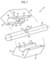
- an indenting assembly generally indicated at 20, which is constructed in accordance with the principles of the present invention.
- terms such as “left”, “right”, “above” and “below” are to be construed in the relative sense. It is to be understood that the present invention is usable in any orientation.
- the optical waveguide extends in a longitudinal direction and the indent or deformation extends in a transverse direction.
- deform means to alter the shape of the optical fiber by pressure or stress.
- fracture means a break, rupture or crack.
- indent means to form an indentation by deforming the optical waveguide, but without mechanically weakening the optical fiber by causing a fracture.
- Either or both of the reflective surfaces can be used for transversely reflecting light carried by the light carrying core of the optical fiber either inwardly or outwardly and then pass through the outer surface of the optical waveguide into a light sensor.
- a light transmitter can inject light transversely through the outside diameter of the optical fiber to be reflected off a reflective surface into the light carrying core of the optical fiber.
- Indenting assembly 20 includes an upper member 22 having a housing 23 and a lower member 24 having a housing 25. Located within upper member 22 is an indenting portion 26.
- the indenting portion 26 can either be made of a light transmissive material or a light reflective material or a combination thereof.
- the indenting portion 26 can be integral to upper member 22 or can be a separate member as depicted in Figure 2A.
- Indenting portion 26 is centrally located within housing 23.
- a portion of a longitudinally extending optical waveguide 28 is positioned between upper member 22 and lower member 24. Although optical waveguide 28 is depicted without an outer cover in Figure 1, the present invention is usable with either an optical fiber (cladding only but no buffer) or an optical cable (cladding and buffer).
- the buffer waveguide on the optical cable does not necessarily need to be removed to use the present invention if the buffer is optically transparent.
- the optical cable has a light carrying core surrounded by an outer cover which would include a cladding and a buffer.
- the buffer must be transparent for the wavelength used, otherwise the buffer has to be stripped.
- the optical waveguide preferably has a circular outer diameter and can also have a rectangular cross-section.
- the cladding has lower index of refraction than the light carrying core and is immediately adjacent. The cladding causes light to travel within the light carrying core by internal reflection.
- the light carrying core of the optical waveguide 28 is formed from a deformable optical material such as plastic.
- Plastic optical fibers permit data transmission rate of up to 3 Gbit/s and are available commercially from companies including, for example, Boston Optical Fiber.
- Plastic can be deformed when subjected to pressure and if indenting portion 26 has the proper geometry, the plastic will deform but not crack or fracture or rupture. Glass is not usable with the present invention.
- Upper member 22 includes a longitudinally extending semi-circular recess 30 having an inner surface 32. Indenting portion 26 is located within recess 30. Lower member 24 has a longitudinally extending semi-circular recess 34 having an inner surface 36. Together, recesses 30, 34 form a circular through bore extending through indenting assembly 20. Recesses 30, 34 are sized to prevent movement of optical waveguide 28 relative to housings 23, 25.
- Upper member 22 has a flat lower surface 38 located on either side of recess 30.
- Lower member 24 has a flat upper surface 40 located on either side of recess 34.
- Upper member 22 has four bolt holes 42 and lower member 24 has four corresponding bolt holes 44.
- Bolt holes 42 and 44 extend through surfaces 38, 40, respectively.
- Other known means of fastening together upper member 22 and lower member 24 can be used, including snapping the assembly together.
- indenting assembly 20 remains secured to the optical waveguide 28 to prevent relaxation of the indented plastic optical material. If the indenting assembly 20 were removed, the plastic light carrying center might distort and reflective surface 57 might not properly reflect the optical signal.
- Recesses 30 and 34 are sized for a particular outside diameter of the optical waveguide 28.
- indenting portion 26 is brought into engagement with an outer diameter of the optical waveguide 28 so as to form an indent or deformation 50 as depicted in Figure 1.
- the indenting portion 26 includes a first surface 52, an intermediate surface 53 and a second surface 54.
- Surfaces 52, 53, 54 form a triangularly shaped indenting portion 26 with intermediate surface 53 being located at the apex of the triangle.
- Surfaces 52 and 54 are flat and surface 53 is preferably curved and is convex as depicted in Figure 1.
- Indent 50 has a first outer flat surface 57, a curved outer intermediate surface 59 and a second flat outer surface 58.
- Outer surfaces 57, 59, 58 can be the cladding or the buffer (if transparent) depending on whether an optical cable or optical fiber is used as the optical waveguide.
- Surfaces 57, 58, 59 correspond in shape to surfaces 52, 53, 54, respectively and are in contact therewith.
- Flat surfaces 57, 59 can be reflective surfaces depending on the angle as discussed below with respect to Figure 3A.
- surfaces 52, 53, 54 extend transversely.
- Surfaces 52, 53 and 54 have a transverse width greater than the width of recess 30.
- an indented optical fiber 28 is depicted with housings 23, 25 of upper member 22 and lower member 24 being omitted, respectively, for clarity.
- an optical signal is being carried by optical waveguide 28 and is travelling from left to right as depicted in Figure 3.
- a portion of the optical signal carried by the optical waveguide 28 strikes first surface 57 and is reflected transversely.
- the optical signal will exit through the outer diameter of the optical cable 28 and through any cladding.
- the optical signal is reflected at a 90° angle because surface 57 is at approximately a 45° angle. The angle at which surface 57 is located can be changed by varying the angle of surface 52.
- the indenter 26 is depicted within indent 50.
- Light travelling in the light carrying core can be reflected off of any one of three surfaces depending on the geometry of the indenter 26, the angle of the cladding, and the material used for the indenter.
- light ray A can be reflected as light ray B, light ray C or light ray D.
- the optical signal will be reflected off of surface 59 of cladding 29 inwardly as light ray B.
- the optical signal will pass through surface 59 and cladding 29 (if the angle ⁇ of surface 59 is less than 45°) and will be reflected of surface 57 of indenter 26 inwardly as light ray C if surface 57 is light reflective.
- the optical signal will be reflected off of surface 50 outwardly as light ray D.
- the reflective surface reflects the optical signal carried by the light carrying core according to Snells law where the angle of reflectance is equal to the angle of incidence.
- indenting portion 26 which permit the indenter and/or the cladding of the optical fiber to be either reflective or light transmissive.
- the discussion for indenting portion 26 is applicable for all alternative indenting portions 26', 26'', 26'''.
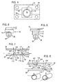
- an alternative indenting portion 26' is depicted.
- Indenting portion 26' has a first surface 60, an intermediate surface 61 and a second surface 62.
- the indent 50 will be formed to conform to the shape of indenter 26'.
- First surface 60 is a curved surface, preferably concave. Surfaces 60 and 62 will be partially light transmissive and partially reflective depending on the curvature of the surfaces 60, 62.
- a convexly curved intermediate surface 61 joins a flat second surface 62.
- Surface 62 is preferably relatively flat and surface 61 is curved. As depicted, light travelling from left to right would pass through the cladding (not shown) adjacent surface 60. Light travelling from right to left would be reflected by the cladding surface adjacent surface 62.
- FIG. 2A A second alternative indenting portion 26'' is depicted in Figure 2A.
- Indenting portion 26' has a first surface 64, an intermediate surface 65 and a second surface 66.
- the first surface 64 has a convex curved shape which will be reflective.
- Intermediate surface 66 has a convexly curved shape and will be light transmissive.
- Second surface 66 is flat. As depicted, light travelling from left to right would be reflected off the cladding (not shown) adjacent surface 64. Light travelling from right to left would pass through the cladding adjacent surface 66.
- a third alternative indenting portion 26''' is depicted in Figure 2A.
- Indenting portion 26''' has a first flat surface 67 and a second flat surface 69 joined by a convexly curved intermediate surface 68. Both surfaces 67 and 69 will be light reflective.
- the indenting portion advantageously does not cause the optical waveguide to crack, rupture or break when the indent is formed. As depicted, light travelling from left to right would be reflected off the cladding (not shown) adjacent surface 67. Light travelling from right to left would be reflected off the cladding (not shown) adjacent surface 69.
- the amount of light reflected by surface 57 can be varied by varying the depth of indent 50.
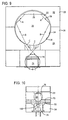
- the depth of indent 50 as defined by surface 59 is approximately ten percent of the diameter of optical waveguide 28 towards a ⁇ filter 70 which is a wavelength filter positioned adjacent to waveguide 28.
- a polarizer 72 is positioned adjacent to and below filter 70 and a light sensor 74 is positioned adjacent to and beneath polarizer 72.
- the indenting portion 26 would be located in upper housing 23 and ⁇ filter 70, polarizer 72 and light sensor 74 would be located in lower housing 25.
- the reflective surface 57 and the light sensor 74 are diametrically opposite from each other as depicted in Figure 3.
- Each of the devices 70, 72, 76 is centrally located relative to indent 50.
- the ⁇ filter 70 is depicted as positioned within a recess 73 in the lower member 24.
- the filter 70 is preferably centrally positioned within the recess 73 and the filter 70 has a larger diameter than the width of recess 34.
- a tab 71 is used to orient filter 70.
- FIG 5-8 various alternative arrangements of indents, filters, polarizers and light sensors are illustrated in schematic form.
- light sensor 74 is located diametrically opposite from indent 50 and light reflected from indent 50 is reflected transversely into sensor 74.
- light sensor 74 has a curved surface 75 which is directly positioned on an outside diameter of the optical waveguide 28, transversely opposite from indent 50.
- the operation of the Figure 5 arrangement is otherwise identical to the Figure 3 arrangement.
- a conforming pad 76 is located diametrically opposite the indent 50 formed in the optical waveguide 28. Located directly above the conforming pad 76 is ⁇ filter 70 and directly above ⁇ filter 70 is a polarizer 72. A light sensor is located directly above polarizer 72. Each of the devices 70, 72, 74, 76 is centrally located relative to indent 50.
- the first recess 100 is formed by a first indenting portion (not depicted for clarity) and the second recess 102 is formed by a second indenting portion (not depicted for clarity).
- the first and second indenting portions can be located in housing 23.
- the first recess 100 includes a first recess surface 104, a second recess surface 108 and an intermediate surface 107 adjacent surfaces 110, 109, 103 of cladding 29.
- the second recess includes a first surface 114, a second surface 118 and an intermediate surface 117 adjacent surfaces 116, 119, 118 of cladding 29.
- light traveling through optical waveguide 28 can travel in opposite directions and be reflected transversely by surfaces 104, 118, respectively, of cladding 29 inwardly through diametrically opposite cladding 29 into light sensors (not shown).
- a first indent 120 is longitudinally spaced and diametrically opposite from a second indent 130.
- an indenter and two light sensors are located in the upper housing 23.
- An indent 120 has a first surface 121, a second surface 124 and an intermediate surface 122 formed by an indenter forming surfaces 127, 126, 129, respectively in cladding 29.
- the indenter is located within upper housing 23.
- the second indent has a first surface 137, an intermediate surface 133 and a second surface 134 formed by indenter 136 having surfaces 132, 133, 135, respectively.
- the indenter is made of a transparent optically transmissive material. A portion of the light traveling from left to right passes through surfaces 121, 127 and is reflected off surface 126 into a light sensor. A portion of the light traveling from left to right is reflected off of surface 134, through the optical waveguide 28 and through the outside diameter into a light sensor.
- Figure 9 depicts light rays being reflected from surface 57 ( Figure 1) into ⁇ filter 70 into light sensor 74. Some of the light rays are reflected by indent 26 into the cladding on the outer diameter of the optical waveguide 28 and then the angle of incidence is such that the light rays are focused by the cladding on the optical waveguide outer diameter into a through hole. Light rays are then impinged on ⁇ filter 70 and are received by light sensor 74.
- Figure 10 expands upon the principles explained with respect to Figure 9 and shows the light rays being further focused by a lens 150 positioned below optical waveguide 28. This arrangement improves the amount of light received by the light sensor 74.
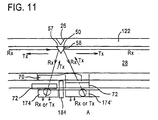
- indent 50 can be formed so that light is reflected off of two surfaces 57, 58 in a direction other than perpendicular.
- surface 57 can be angled so that an optical signal is reflected so the light sensor is positioned longitudinally offset relative to indent 50.
- a pair of light sensors or transmitters 174, 174' are each longitudinally offset relative to indent 50 so that surface 57 reflects light into light sensor 174 through filter 70 and surface 58 reflects light into light sensor 174' through filter 70.
- a spacer 184 is positioned between light sensors 174 and 174' to prevent dispersed light from impinging on the light sensors 174, 174'. In this manner, a single indent 50 can be used to transmit/receive two optical signals, traveling in two directions in the optical waveguide 28.
- a light transmitter can be substituted for a light sensor.
- light could be injected into the optical waveguide 28 and reflected off of indent 50.
- arrays of fibers and detectors and receiving diodes can be used with the present invention.
- the tapped light can also be carried directly to an integrated circuit such as OPTOFET transformer amplifier.
Applications Claiming Priority (2)
| Application Number | Priority Date | Filing Date | Title |
|---|---|---|---|
| US20977298A | 1998-12-11 | 1998-12-11 | |
| US209772 | 1998-12-11 |
Publications (2)
| Publication Number | Publication Date |
|---|---|
| EP1008876A2 true EP1008876A2 (fr) | 2000-06-14 |
| EP1008876A3 EP1008876A3 (fr) | 2003-03-26 |
Family
ID=22780212
Family Applications (1)
| Application Number | Title | Priority Date | Filing Date |
|---|---|---|---|
| EP99123869A Withdrawn EP1008876A3 (fr) | 1998-12-11 | 1999-12-01 | Prise à fibres optiques et procédé pour dériver un signal optique d'un câble optique |
Country Status (3)
| Country | Link |
|---|---|
| EP (1) | EP1008876A3 (fr) |
| JP (1) | JP2000180653A (fr) |
| CA (1) | CA2291905A1 (fr) |
Cited By (7)
| Publication number | Priority date | Publication date | Assignee | Title |
|---|---|---|---|---|
| WO2002095470A1 (fr) * | 2001-05-23 | 2002-11-28 | Infineon Technologies Ag | Module electro-optique destine a l'emission et / ou a la reception de signaux optiques d'au moins deux voies de donnees optiques |
| EP1311882A1 (fr) * | 2000-07-25 | 2003-05-21 | Optical Air Data Systems, LP | Systeme a fibre optique |
| EP1357684A2 (fr) * | 2002-04-26 | 2003-10-29 | Agilent Technologies, Inc. | Systèmes émetteur-récepteur optiques et méthodes correspondantes |
| EP1417522A1 (fr) * | 2001-07-24 | 2004-05-12 | The Government of the United States of America as represented by the Secretary of the Navy | Procede de couplage de rayonnement lumineux dans des sources de fibres a pompage de gaine par utilisation d'un miroir integre |
| EP1442328A1 (fr) * | 2001-11-08 | 2004-08-04 | Hantech Co., Ltd | Dispositif optique renfermant un bloc matriciel de fibres optiques |
| WO2004083917A2 (fr) * | 2003-03-17 | 2004-09-30 | Eigenlight Corporation | Prise de fibre optique a faible perte a surface reflechissante integree |
| US7058267B2 (en) | 2002-11-12 | 2006-06-06 | Toptica Photonics Ag | Method for manufacturing of an optical fiber with a decoupling interface for scattered light, use of an optical fiber and device for monitoring of the light power guided through an optical fiber |
Families Citing this family (3)
| Publication number | Priority date | Publication date | Assignee | Title |
|---|---|---|---|---|
| JP2006171642A (ja) * | 2004-12-20 | 2006-06-29 | Sony Corp | 光導波シート、光電子装置およびそれらの製造方法 |
| EP2073406B1 (fr) * | 2007-12-17 | 2014-02-12 | Siemens Aktiengesellschaft | Machine dotée d'une communication optique entre une première partie de machine et une seconde partie de machine pivotant en fonction de la première partie de machine |
| JP5273616B2 (ja) * | 2009-10-20 | 2013-08-28 | 独立行政法人情報通信研究機構 | 光エネルギー伝送装置 |
Citations (9)
| Publication number | Priority date | Publication date | Assignee | Title |
|---|---|---|---|---|
| JPS6170512A (ja) * | 1984-09-14 | 1986-04-11 | Nippon Telegr & Teleph Corp <Ntt> | 光フアイバ伝搬光検出方法及びその検出器 |
| GB2168165A (en) * | 1984-12-10 | 1986-06-11 | Electronic Components Ltd | Tap for data transmission system |
| WO1990002349A1 (fr) * | 1988-08-31 | 1990-03-08 | Raynet Corporation | Procede de deformation d'une fibre optique polymere pour former des prises |
| JPH05116592A (ja) * | 1991-10-30 | 1993-05-14 | Ishikawajima Harima Heavy Ind Co Ltd | 車体衝突検出装置 |
| GB2266160A (en) * | 1992-04-16 | 1993-10-20 | Ericsson Telefon Ab L M | Tapping into optical waveguides |
| US5305401A (en) * | 1990-12-21 | 1994-04-19 | Thomson-Csf | Optical connection device and data processing apparatus fitted with optical transmission means |
| DE4406335A1 (de) * | 1994-02-28 | 1995-09-07 | Ant Nachrichtentech | Anordnung zur strahlteilenden Abzweigung oder zur wellenlängenselektiven Abzweigung oder Einkopplung von Licht und Verfahren zur Herstellung der Anordnung |
| WO1996007117A1 (fr) * | 1994-08-29 | 1996-03-07 | Akzo Nobel N.V. | Connecteur destine a des structures de guide d'onde optique polymere |
| DE19711121A1 (de) * | 1997-03-05 | 1998-10-01 | Siemens Ag | Verzweigende Lichtwellenleiteranordnung |
-
1999
- 1999-12-01 EP EP99123869A patent/EP1008876A3/fr not_active Withdrawn
- 1999-12-09 CA CA002291905A patent/CA2291905A1/fr not_active Abandoned
- 1999-12-10 JP JP11352398A patent/JP2000180653A/ja not_active Withdrawn
Patent Citations (9)
| Publication number | Priority date | Publication date | Assignee | Title |
|---|---|---|---|---|
| JPS6170512A (ja) * | 1984-09-14 | 1986-04-11 | Nippon Telegr & Teleph Corp <Ntt> | 光フアイバ伝搬光検出方法及びその検出器 |
| GB2168165A (en) * | 1984-12-10 | 1986-06-11 | Electronic Components Ltd | Tap for data transmission system |
| WO1990002349A1 (fr) * | 1988-08-31 | 1990-03-08 | Raynet Corporation | Procede de deformation d'une fibre optique polymere pour former des prises |
| US5305401A (en) * | 1990-12-21 | 1994-04-19 | Thomson-Csf | Optical connection device and data processing apparatus fitted with optical transmission means |
| JPH05116592A (ja) * | 1991-10-30 | 1993-05-14 | Ishikawajima Harima Heavy Ind Co Ltd | 車体衝突検出装置 |
| GB2266160A (en) * | 1992-04-16 | 1993-10-20 | Ericsson Telefon Ab L M | Tapping into optical waveguides |
| DE4406335A1 (de) * | 1994-02-28 | 1995-09-07 | Ant Nachrichtentech | Anordnung zur strahlteilenden Abzweigung oder zur wellenlängenselektiven Abzweigung oder Einkopplung von Licht und Verfahren zur Herstellung der Anordnung |
| WO1996007117A1 (fr) * | 1994-08-29 | 1996-03-07 | Akzo Nobel N.V. | Connecteur destine a des structures de guide d'onde optique polymere |
| DE19711121A1 (de) * | 1997-03-05 | 1998-10-01 | Siemens Ag | Verzweigende Lichtwellenleiteranordnung |
Non-Patent Citations (2)
| Title |
|---|
| PATENT ABSTRACTS OF JAPAN vol. 010, no. 241 (P-488), 20 August 1986 (1986-08-20) -& JP 61 070512 A (NIPPON TELEGR & TELEPH CORP), 11 April 1986 (1986-04-11) * |
| PATENT ABSTRACTS OF JAPAN vol. 017, no. 483 (M-1472), 2 September 1993 (1993-09-02) -& JP 05 116592 A (ISHIKAWAJIMA HARIMA HEAVY IND CO LTD), 14 May 1993 (1993-05-14) * |
Cited By (15)
| Publication number | Priority date | Publication date | Assignee | Title |
|---|---|---|---|---|
| EP1311882A1 (fr) * | 2000-07-25 | 2003-05-21 | Optical Air Data Systems, LP | Systeme a fibre optique |
| EP1311882A4 (fr) * | 2000-07-25 | 2005-05-11 | Optical Air Data Systems Lp | Systeme a fibre optique |
| US6757460B2 (en) | 2001-05-23 | 2004-06-29 | Infineon Technologies Ag | Electro-optical module for transmitting and/or receiving optical signals on at least two optical data channels |
| WO2002095470A1 (fr) * | 2001-05-23 | 2002-11-28 | Infineon Technologies Ag | Module electro-optique destine a l'emission et / ou a la reception de signaux optiques d'au moins deux voies de donnees optiques |
| EP1417522A1 (fr) * | 2001-07-24 | 2004-05-12 | The Government of the United States of America as represented by the Secretary of the Navy | Procede de couplage de rayonnement lumineux dans des sources de fibres a pompage de gaine par utilisation d'un miroir integre |
| EP1417522A4 (fr) * | 2001-07-24 | 2006-08-02 | Us Gov Sec Navy | Procede de couplage de rayonnement lumineux dans des sources de fibres a pompage de gaine par utilisation d'un miroir integre |
| EP1442328A1 (fr) * | 2001-11-08 | 2004-08-04 | Hantech Co., Ltd | Dispositif optique renfermant un bloc matriciel de fibres optiques |
| EP1442328A4 (fr) * | 2001-11-08 | 2005-11-16 | Hantech Co Ltd | Dispositif optique renfermant un bloc matriciel de fibres optiques |
| US7010192B2 (en) | 2001-11-08 | 2006-03-07 | Hantech Co., Ltd. | Optical fiber array block embedding optical device therein |
| EP1357684A3 (fr) * | 2002-04-26 | 2005-04-06 | Agilent Technologies, Inc. | Systèmes émetteur-récepteur optiques et méthodes correspondantes |
| EP1357684A2 (fr) * | 2002-04-26 | 2003-10-29 | Agilent Technologies, Inc. | Systèmes émetteur-récepteur optiques et méthodes correspondantes |
| US7184669B2 (en) | 2002-04-26 | 2007-02-27 | Avago Technologies Fiber Ip (Singapore) Pte. Ltd. | Optical transceiver systems and methods |
| US7058267B2 (en) | 2002-11-12 | 2006-06-06 | Toptica Photonics Ag | Method for manufacturing of an optical fiber with a decoupling interface for scattered light, use of an optical fiber and device for monitoring of the light power guided through an optical fiber |
| WO2004083917A2 (fr) * | 2003-03-17 | 2004-09-30 | Eigenlight Corporation | Prise de fibre optique a faible perte a surface reflechissante integree |
| WO2004083917A3 (fr) * | 2003-03-17 | 2004-12-23 | Eigenlight Corp | Prise de fibre optique a faible perte a surface reflechissante integree |
Also Published As
| Publication number | Publication date |
|---|---|
| CA2291905A1 (fr) | 2000-06-11 |
| JP2000180653A (ja) | 2000-06-30 |
| EP1008876A3 (fr) | 2003-03-26 |
Similar Documents
| Publication | Publication Date | Title |
|---|---|---|
| EP1008876A2 (fr) | Prise à fibres optiques et procédé pour dériver un signal optique d'un câble optique | |
| EP0168261B1 (fr) | Connecteur pour rayon à haute énergie | |
| JP5875984B2 (ja) | 角度劈開光ファイバ並びにその製造及び使用方法 | |
| US5315680A (en) | Optical fiber connector structure including three ferrules and an optical baffle | |
| US20080019646A1 (en) | Optical fiber mechanical splice connector | |
| JPH0618793A (ja) | 可変光減衰装置 | |
| WO2000039617A3 (fr) | Reseau de fibres place dans un tube | |
| IL206115A (en) | Stub having an optical fiber | |
| WO2000037914A3 (fr) | Sonde manometrique a reseau de bragg | |
| US4950046A (en) | Fiber optic coupler | |
| WO2011066122A2 (fr) | Guide d'ondes plan et couplage de fibre optique | |
| WO2000003279A1 (fr) | Procede et dispositif de connexion de fibres optiques | |
| CA2336886A1 (fr) | Procede et appareil servant a aligner des fibres optiques | |
| JP2002124687A (ja) | 双方向光通信器および双方向光通信装置並びに双方向光通信器の組み立て方法 | |
| WO2000003281A1 (fr) | Procede et dispositif de presentation de fibres optiques en utilisant un gabarit de presentation | |
| KR100254086B1 (ko) | 광섬유접속기 | |
| KR100309119B1 (ko) | 광파이버접속장치 | |
| JPH09145957A (ja) | 光コネクタ | |
| US6445854B1 (en) | Optical fiber having first and second reflective surfaces and method of operation | |
| JPH06501565A (ja) | 光タップ | |
| GB2158607A (en) | Fiber optic coupler | |
| US20090080833A1 (en) | Apparatus and methods for remakeable connections to optical waveguides | |
| US6470114B1 (en) | Retroreflective conductors for optical fiber interconnects | |
| EP1043608A1 (fr) | Dispositif optique et module optique a dispositif optique | |
| US6519392B2 (en) | Optical tap collimator using an uncoated GRIN lens |
Legal Events
| Date | Code | Title | Description |
|---|---|---|---|
| PUAI | Public reference made under article 153(3) epc to a published international application that has entered the european phase |
Free format text: ORIGINAL CODE: 0009012 |
|
| AK | Designated contracting states |
Kind code of ref document: A2 Designated state(s): AT BE CH CY DE DK ES FI FR GB GR IE IT LI LU MC NL PT SE |
|
| AX | Request for extension of the european patent |
Free format text: AL;LT;LV;MK;RO;SI |
|
| RIN1 | Information on inventor provided before grant (corrected) |
Inventor name: WINDEBANK, ROBERT W. |
|
| PUAL | Search report despatched |
Free format text: ORIGINAL CODE: 0009013 |
|
| AK | Designated contracting states |
Kind code of ref document: A3 Designated state(s): AT BE CH CY DE DK ES FI FR GB GR IE IT LI LU MC NL PT SE Designated state(s): AT BE CH CY DE DK ES FI FR GB GR IE IT LI LU MC NL PT SE |
|
| AX | Request for extension of the european patent |
Extension state: AL LT LV MK RO SI |
|
| RIC1 | Information provided on ipc code assigned before grant |
Ipc: 7G 02B 6/28 B Ipc: 7G 02B 6/42 B Ipc: 7G 02B 6/26 A |
|
| AKX | Designation fees paid | ||
| REG | Reference to a national code |
Ref country code: DE Ref legal event code: 8566 |
|
| STAA | Information on the status of an ep patent application or granted ep patent |
Free format text: STATUS: THE APPLICATION IS DEEMED TO BE WITHDRAWN |
|
| 18D | Application deemed to be withdrawn |
Effective date: 20030927 |