EP1014300A1 - Capacitive modulation in a electromagnetic transponder - Google Patents
Capacitive modulation in a electromagnetic transponder Download PDFInfo
- Publication number
- EP1014300A1 EP1014300A1 EP99410180A EP99410180A EP1014300A1 EP 1014300 A1 EP1014300 A1 EP 1014300A1 EP 99410180 A EP99410180 A EP 99410180A EP 99410180 A EP99410180 A EP 99410180A EP 1014300 A1 EP1014300 A1 EP 1014300A1
- Authority
- EP
- European Patent Office
- Prior art keywords
- transponder
- modulation
- circuit
- terminal
- electronic circuit
- Prior art date
- Legal status (The legal status is an assumption and is not a legal conclusion. Google has not performed a legal analysis and makes no representation as to the accuracy of the status listed.)
- Granted
Links
Images

Classifications
-
- G—PHYSICS
- G06—COMPUTING; CALCULATING OR COUNTING
- G06K—GRAPHICAL DATA READING; PRESENTATION OF DATA; RECORD CARRIERS; HANDLING RECORD CARRIERS
- G06K19/00—Record carriers for use with machines and with at least a part designed to carry digital markings
- G06K19/06—Record carriers for use with machines and with at least a part designed to carry digital markings characterised by the kind of the digital marking, e.g. shape, nature, code
- G06K19/067—Record carriers with conductive marks, printed circuits or semiconductor circuit elements, e.g. credit or identity cards also with resonating or responding marks without active components
- G06K19/07—Record carriers with conductive marks, printed circuits or semiconductor circuit elements, e.g. credit or identity cards also with resonating or responding marks without active components with integrated circuit chips
- G06K19/077—Constructional details, e.g. mounting of circuits in the carrier
- G06K19/07749—Constructional details, e.g. mounting of circuits in the carrier the record carrier being capable of non-contact communication, e.g. constructional details of the antenna of a non-contact smart card
- G06K19/07773—Antenna details
- G06K19/07777—Antenna details the antenna being of the inductive type
-
- G—PHYSICS
- G06—COMPUTING; CALCULATING OR COUNTING
- G06K—GRAPHICAL DATA READING; PRESENTATION OF DATA; RECORD CARRIERS; HANDLING RECORD CARRIERS
- G06K19/00—Record carriers for use with machines and with at least a part designed to carry digital markings
- G06K19/06—Record carriers for use with machines and with at least a part designed to carry digital markings characterised by the kind of the digital marking, e.g. shape, nature, code
- G06K19/067—Record carriers with conductive marks, printed circuits or semiconductor circuit elements, e.g. credit or identity cards also with resonating or responding marks without active components
- G06K19/07—Record carriers with conductive marks, printed circuits or semiconductor circuit elements, e.g. credit or identity cards also with resonating or responding marks without active components with integrated circuit chips
- G06K19/0723—Record carriers with conductive marks, printed circuits or semiconductor circuit elements, e.g. credit or identity cards also with resonating or responding marks without active components with integrated circuit chips the record carrier comprising an arrangement for non-contact communication, e.g. wireless communication circuits on transponder cards, non-contact smart cards or RFIDs
Definitions
- the present invention relates to the field of transponders electromagnetic, i.e. transceivers (generally mobile) likely to be questioned without contact and wireless by a unit (generally fixed), called reading terminal and writing.
- the present invention relates, more particularly, transponders without autonomous power supply, that is to say which extract the power necessary for the circuits radiated high frequency field by an antenna of the read and write unit.
- the invention applies to such transponders, whether they are transponders read-only, i.e. suitable for operation with a terminal simply reading the data from the transponder, or read-write transponders whose data they contain can be modified by the terminal.
- the electromagnetic transponders are based on the use of oscillating circuits, transponder side and unit side read-write. These circuits are intended to be coupled by near magnetic field when the transponder enters the read-write unit field.
- the scope of a system to transponder i.e. the maximum distance from the terminal to which a transponder is activated (awake) depends, in particular, the size of the transponder antenna, the excitation frequency of the coil of the oscillating circuit generating the field magnetic, and the intensity of this excitation.
- FIG. 1 very schematically represents a classic example of a data exchange system between a unit 1 read-write and a transponder 10.
- unit 1 is essentially made up of an oscillating circuit formed by an inductor L1 in series with a capacitor C1 between an output terminal 2 of an antenna coupler 3 (COUP) and a terminal 4 at a reference potential (generally, the mass).
- the coupler 3 receives a signal fl from a oscillator 5 (OSC) and constituting a high frequency carrier.
- the signal f1 is used, in the absence of data transmission from the terminal 1 to transponder 10, from "energy source” to activate the transponder 10 if it goes into the field.
- a modulator 6 delivers a data signal data from data to be transmitted, received from an input e and coming from an electronic system (not shown).
- the midpoint of the series association of the capacitor C1 with inductance L1 constitutes, in the example shown in FIG. 1, an rx terminal for sampling a data signal, received from a transponder 10 to a demodulator 7 (DEM).
- An output s of the demodulator communicates the data received from the transponder 10 to the electronic system of the read-write unit.
- the demodulator 7 receives a signal from the oscillator 5 f2 (most often of the same frequency as the signal f1) for allow demodulation. If necessary, demodulation is made from a signal taken from the coupler terminals antenna 3 and not across the inductor L1.
- the inductance L1 of unit 1 By excitation by means of the signal f1, the inductance L1 of unit 1 generates a low intensity high frequency field.
- Transponder side 10 an L2 choke, in parallel with a capacitor C2, forms an oscillating circuit (called circuit resonating in reception) parallel and intended to capture the field generated by the oscillating circuit of unit 1.
- the resonant circuit (L2, C2) of transponder 10 is tuned to the frequency of oscillating circuit (L1, C1) of unit 1.
- Terminals 11, 12 of the resonant circuit are connected to two input terminals alternative of a righting bridge 13 constituted, by example, of four diodes D1, D2, D3, D4.
- the anode of the diode Dl is connected to the terminal 11, as well as the cathode of diode D3.
- the anode of diode D2 and the cathode of diode D4 are connected to terminal 12.
- the cathodes of diodes D1 and D2 constitute a positive terminal 14 of straightened outlet.
- the anodes of diodes D3 and D4 constitute a reference terminal 15 of the rectified voltage.
- a Ca capacitor is connected in parallel with the rectified output terminals 14, 15 of bridge 13 so as to filter the rectified voltage delivered by the bridge.
- transponder 10 When transponder 10 is in the field of unit 1, a high frequency voltage is generated at the terminals of the resonant circuit. This voltage, rectified by bridge 13 and smoothed by the capacitor Ca, provides a supply voltage Goes to electronic transponder circuits via of a voltage regulator 16 (BACKUP). Electronic circuits of the transponder have been symbolized in FIG. 1 by a block 17 (P). It is generally a chip (integrating the most often the regulator 16) containing at least one memory and one processor.
- block 17 controls a modulation stage (retromodulation) of the resonant circuit (L2, C2).
- This modulation stage usually consists of an electronic switch (a transistor 18) and a resistor R, associated in series between the terminals 14 and 15.
- the transistor 18 is controlled at a frequency significantly lower (usually with a ratio of at least 10) with respect to the frequency f1 of the circuit excitation signal oscillating unit 1.
- the oscillating circuit of the transponder is therefore subject to additional depreciation compared to the load consisting of regulator 16 and circuit 17 when the switch 18 is closed. The voltage drops across the winding L2 so that the transponder takes a quantity of energy higher in the high frequency field.
- Another method is to detect the variation of phase due to this change in load on the oscillating circuit of unit 1.
- amplitude modulation representing, or the entire amplitude of the signal f1, (modulation all or nothing), or a small portion (of the order of 10%) of this amplitude due to the power requirement of the transponder 10.
- the modulation is transmitted digitally, by jumping between two binary levels.
- the tuning frequency of the oscillating circuits conditions the transmission rate as far as the frequency modulation, via switch 18 on the transponder side, must be significantly lower than the carrier frequency used to supply power to the transponders. Therefore, the higher the feed carrier frequency, the higher the flow can be important.
- the frequency of the carrier fl is 13.56 MHz and the frequency of the switch control pulses 18, transponder side, is 847 kHz (16 times less).
- a first drawback is that there are “transmission holes”, that is, distances between the transponder and the terminal at which the latter does not detect the transponder even when it is in its field. These transmission holes occur when the transponder is very close to the read-write unit, i.e. when the distance between the two coupling elements L1 and L2 inductive is low compared to the operating range of the system. For example, for application to systems with low distance at a frequency of 13.56 MHz, the range is the order of 10 centimeters and we see appear losses of detection when the transponder is less than three centimeters of the read-write unit.
- a classic solution to solve this problem is to force a minimum gap between the transponder and unit 1.
- a disadvantage of such a solution is that it reduces the scope of the system.
- transponder systems classics Another disadvantage of transponder systems classics is that the use of a resistance R in the stage of modulation of the transponder 10 causes dissipation during the modulation by the transponder. Now, as mentioned earlier, the transponder is not powered independently but draws its power from the high frequency field from of the read-write system. Therefore, any consumption energy should be minimized.
- An object of the present invention is to overcome the disadvantages of conventional transponder systems.
- the present invention aims, in particular, to propose a new transponder architecture that avoids "holes" transmission while preserving the maximum range of reach at system.
- the present invention also aims to provide a solution that is particularly simple to implement and economical from the point of view of the components used, so as to favor miniaturization of the transponder.
- the present invention further aims to minimize the energy consumption of the transponder.
- the solution recommended by the present invention is to use, on the transponder side, an active modulation element on the resonant frequency of the oscillating circuit and not on its amplitude as in the case of a resistance. So this invention proposes to slightly detune the oscillating circuits during modulation (retromodulation) by the transponder.
- the present invention originates from a new analysis of the causes of transmission losses in systems with electromagnetic transponders.
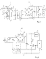
- FIG. 2 represents, for several deviations between a transponder and a read-write unit, examples of voltage-frequency characteristics, where the voltage represents the remote supply voltage of the transponder, for example, the voltage V2 at the terminals of the inductor L2 of the transponder, and where f corresponds to the excitation frequency of the terminal's oscillating circuit.
- the different curves illustrated in Figure 2 are plotted for oscillating circuits tuned to position fi, that is to say the resonance frequency of the circuits L1, C1 and L2, C2.
- the curves g1, g2, g3, g4, g5 and g6 indicate distances decreasing between the transponder and the read-write system.
- the curve g1 which represents a small dome centered on the tuning frequency fi, corresponds substantially at the system range limit.
- the curve g4 illustrates the position optimal coupling, i.e.
- the pace of the voltage as a function of frequency represents, for these distances, two peaks on either side of the tuning frequency linked one to the other by a minimum (hole) at the tuning frequency.
- the more the distance decreases the more the two peaks deviate from each other and the lower the minimum is close to zero voltage.
- the present invention proposes to use a modulation acting on the resonance frequency of the oscillating circuit by modifying the equivalent capacity of the oscillating circuit on the transponder side. Note that, in the absence retromodulation by transponder, oscillating circuits remain tuned, i.e. with the same frequency of resonance. So only when there is a need to transmit data from the transponder to the base which is shifted slightly the resonance frequency of the oscillating circuit of the transponder so as to leave the area of possible "holes" depending on the distance between the transponder and the terminal, and allow thus transmitting data from the transponder to the thick headed.
- the transponder is necessarily detected by the terminal insofar as, in such an electromagnetic system, the transponder necessarily starts with an approach from the far range distance to a longer distance low.
- Capacitive modulation does not disturb resonance in terms of its magnitude from the time the low value of the capacity, which is added to the capacity of the circuit resonant, maintains the coupling in an area close to the chord. Therefore, as there is no longer a resistive voltage drop additional, the remote power supply is preserved.
- Capacitive modulation directly influences the phase of the voltage across the inductance L1 of the terminal because, by coupling, this modulation is brought back on this inductance and it introduces a variation essentially on the imaginary part of the complex impedance of circuit L1, C1, therefore directly on the phase.
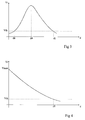
- Figures 3 and 4 illustrate, depending on the distance d (difference between the transponder and the terminal), the amplitudes Vr of the signal recovered, at output s (figure 1) on the terminal side, following retromodulations, respectively resistive and capacitive, for a system in which the oscillating circuits are (in no modulation) granted.
- FIG. 3 shows an example of a characteristic in resistive retromodulation.
- the amplitude of the retromodulation has a shape approximately in bell, centered on a gap d4 corresponding to an optimal coupling (curve g4 in Figure 2).
- the amplitude of the retromodulation is below a Vth threshold of detection by the demodulator. This corresponds to the dl limit of scope of the system.
- the amplitude is below the terminal detection threshold Vth, where the drop in voltage linked to the modulation is superimposed on a remote feed hole.
- Figure 4 shows a similar example, but for capacitive modulation.
- the shape of the amplitude-distance characteristic here has an approximately linear decrease since a maximum Vmax until passing below the detection threshold Vth when the distance reaches the system range limit dl. So the remote feed holes have no effect on capacitive retromodulation.
- a first solution would be to connect a capacitor in series with a control switch between the terminals 11 and 12, that is to say in parallel on the capacitor C2 of the oscillating circuit.
- an object of the present invention is to propose a new solution allowing a modification of the capacity equivalent of the oscillating circuit by simple means.
- the present invention aims to allow the control, by means of simple MOS transistors, of a means of capacitive modulation of the oscillating circuit of the transponder.
- the present invention also aims to ensure that it is not no need to modify the type of classic command operated at circuit means (17, figure 1) in the case of a modulation stage resistive.
- the present invention provides a electromagnetic transponder of the type comprising a circuit oscillating upstream of a rectification means capable of providing a DC supply voltage of an electronic circuit, the electronic circuit comprising means for transmitting digitally encoded information, and the transponder comprising two capacitive modulation means, respectively associated with each end terminal of the inductive element of the oscillating circuit, a reference terminal of each modulation means being connected to the circuit supply reference potential electronic, downstream of the rectifying means.
- each capacitive modulation means consists of a transistor MOS connected between one of the end terminals of the inductor of the oscillating circuit and the voltage reference terminal continuous supply of the electronic circuit, the grid each transistor receiving the modulation signal emitted by the electric circuit.
- each transistor constitutes a control switch of a capacitor with which it is associated in series, between one of end terminals of the inductive element of the oscillating circuit and the reference terminal of the electronic circuit.
- the inductive element of the oscillating circuit includes a midpoint constituting the reference potential of the electronic circuit.
- the transponder further comprises a resistive modulation means, in parallel on a voltage filtering capacitor rectified delivered by said rectifying means.
- the capacitive and resistive modulation means are controlled to from the same signal.
- the resistive modulation means is controlled through a circuit validation of the control signal of said modulation means capacitive.
- the invention also relates to a transmission system.
- electromagnetic of the type comprising a read-write terminal generating an electromagnetic field suitable for cooperation with at least one transponder when the latter enters this field.
- FIG. 5 represents a first embodiment a 10 'transponder according to the present invention.
- this transponder is made from a circuit oscillating formed by an inductance L2 and a capacitor C2 connected in parallel between two terminals 11, 12 of alternative input of a bridge 13.
- Two rectified output terminals 14, 15 of the bridge 13 provide, via a capacitor Ca filtering, a supply voltage of an electronic unit 17, for example a P processor.
- the voltage block 17 is supplied by a regulator circuit 16 (BACKUP).
- BACKUP regulator circuit 16
- the regulation illustrated as being a series type regulation can also be of type parallel to by means of a regulator connected between terminals 14 and 15.
- two capacitors of modulation C3 and C4 are each associated in series with a switch (for example, a MOS transistor) K1, K2, respectively between terminals 11 and 12 and terminal 15.
- a switch for example, a MOS transistor
- K1, K2 a MOS transistor
- a first terminal of capacitor C3 is connected to terminal 11 while that its other terminal is connected, via the transistor K1, at terminal 15.
- a first terminal of capacitor C4 is connected to terminal 12 while its other terminal is connected, via a transistor K2, to terminal 15.
- two capacities are used respectively associated with each sign of the alternating voltage V2.
- the two capacitors C3 and C4 are therefore of the same value, appropriate to perform the desired modulation.
- the two K1 transistors and K2 are controlled by block 17, preferably from a same signal.
- a feature of the present invention is that thanks to the splitting of the capacitors modulation, you can have a reference point (line 15) for controlling switches K1 and K2. So if switches K1 and K2 are made up of MOS transistors N channel, it is now possible, by a logic signal from the block 17, to control these switches all or nothing so to provide the necessary modulation to transmit data to the fixed read-write terminal.
- a retromodulation circuit resistive consisting, as for a conventional transponder, of a resistance R associated with a switch 18 in series between the terminals 14 and 15.
- R a resistance associated with a switch 18 in series between the terminals 14 and 15.
- FIG. 6 shows a second embodiment a 10 "transponder according to the present invention.
- This transponder 10 "contains substantially the same elements as those of the figure 5.
- a feature of this second embodiment is to provide an inductor L2 'at midpoint 15'. This point medium then serves as a reference line for continuous feeding of the electronic circuit on the transponder side. So, a first terminal 11 of the winding L2 'is connected to the anode of a diode rectifier Dl 'whose cathode constitutes the supply terminal 14 of the transponder side circuit. A second terminal 12 of winding L2 'is connected to the anode of a rectifying diode D4 'whose cathode is connected to terminal 14.
- the capacitor C2 is, as before, connected between terminals 11 and 12. Likewise, each modulation stage capacitive is respectively connected between terminals 11 and 15 ' and between terminals 12 and 15 '.
- a first capacitor C3, associated in series with a first switch K1 is connected between terminals 11 and 15 'while a second capacitor C4, associated in series with a second switch K2, is connected between terminals 12 and 15 '.
- the respective control terminals switches K1 and K2 (for example, the respective grids MOS transistors) are connected to an output terminal of the block electronics 17 (for example, the transponder processor).
- a filtering capacitor Ca is connected between terminals 14 and 15 'to filter the supply voltage of the electronic circuit and, in particular, supply the regulator 16.
- a resistive modulation stage consisting of a resistor R associated in series with a switch 18 between terminals 14 and 15 '. Note however that, as for the embodiment In Figure 5, this resistive modulation stage is optional.
- An advantage of the second embodiment is that two diodes are sufficient to carry out the rectification necessary for the power supply to the electronic circuit of the transponder.
- this embodiment requires a point inductor middle.
- the choice between the first and the second embodiment will depend on the application and, in particular, on the frequency of use which conditions the size of the inductor necessary.
- the modulation capacities are constituted by the intrinsic capacities of MOS transistors constituting switches K1 and K2.
- the drain / source capacitance of MOS transistors we use the drain / source capacitance of MOS transistors, so only two MOS transistors are needed.
- the capacity values required for retromodulation by the transponder are compatible with the capacities intrinsic of the MOS transistors produced. Note that the control signals must then be adapted, the capacities parasites being functionally present only when the transistors are blocked.
- the present invention is capable of various variants and modifications which will appear to the man of art.
- the respective dimensions of the capacitors, resistors and inductors, as well as other components of a transponder according to the present invention are at the scope of the skilled person depending on the application.
- the present invention finds a special interest in electromagnetic transmission systems operating at high frequency. Indeed, at such frequencies, the displacement speeds of the transponders by users are negligible compared to the transmission rate information so the electromagnetic coupling is not significantly changed during an exchange of information.
Landscapes
- Engineering & Computer Science (AREA)
- Computer Networks & Wireless Communication (AREA)
- Computer Hardware Design (AREA)
- Microelectronics & Electronic Packaging (AREA)
- Physics & Mathematics (AREA)
- General Physics & Mathematics (AREA)
- Theoretical Computer Science (AREA)
- Near-Field Transmission Systems (AREA)
- Radar Systems Or Details Thereof (AREA)
Abstract
Description
La présente invention concerne le domaine des transpondeurs électromagnétiques, c'est-à-dire des émetteurs-récepteurs (généralement mobiles) susceptibles d'être interrogés sans contact et sans fil par une unité (généralement fixe), dite borne de lecture et d'écriture. La présente invention concerne, plus particulièrement, les transpondeurs dépourvus d'alimentation autonome, c'est-à-dire qui extraient l'alimentation nécessaire aux circuits électroniques qu'ils comportent, du champ haute fréquence rayonné par une antenne de l'unité de lecture et d'écriture. L'invention s'applique à de tels transpondeurs, qu'il s'agisse de transpondeurs à lecture seulement, c'est-à-dire propres à fonctionner avec une borne se contentant de lire les données du transpondeur, ou à des transpondeurs lecture-écriture dont les données qu'ils contiennent peuvent être modifiées par la borne.The present invention relates to the field of transponders electromagnetic, i.e. transceivers (generally mobile) likely to be questioned without contact and wireless by a unit (generally fixed), called reading terminal and writing. The present invention relates, more particularly, transponders without autonomous power supply, that is to say which extract the power necessary for the circuits radiated high frequency field by an antenna of the read and write unit. The invention applies to such transponders, whether they are transponders read-only, i.e. suitable for operation with a terminal simply reading the data from the transponder, or read-write transponders whose data they contain can be modified by the terminal.
Les transpondeurs électromagnétiques sont basés sur l'emploi de circuits oscillants, côté transpondeur et côté unité de lecture-écriture. Ces circuits sont destinés à être couplés par champ magnétique proche lorsque le transpondeur entre dans le champ de l'unité de lecture-écriture. La portée d'un système à transpondeur, c'est-à-dire la distance maximale de la borne à laquelle un transpondeur est activé (réveillé) dépend, notamment, de la taille de l'antenne du transpondeur, de la fréquence d'excitation de la bobine du circuit oscillant engendrant le champ magnétique, et de l'intensité de cette excitation.The electromagnetic transponders are based on the use of oscillating circuits, transponder side and unit side read-write. These circuits are intended to be coupled by near magnetic field when the transponder enters the read-write unit field. The scope of a system to transponder, i.e. the maximum distance from the terminal to which a transponder is activated (awake) depends, in particular, the size of the transponder antenna, the excitation frequency of the coil of the oscillating circuit generating the field magnetic, and the intensity of this excitation.
La figure 1 représente, de façon très schématique, un
exemple classique de système d'échange de données entre une unité
1 de lecture-écriture et un transpondeur 10.FIG. 1 very schematically represents a
classic example of a data exchange system between a
Généralement, l'unité 1 est essentiellement constituée
d'un circuit oscillant formé d'une inductance L1 en série avec un
condensateur C1 entre une borne 2 de sortie d'un coupleur d'antenne
3 (COUP) et une borne 4 à un potentiel de référence (généralement,
la masse). Le coupleur 3 reçoit un signal fl, issu d'un
oscillateur 5 (OSC) et constituant une porteuse haute fréquence.
Le signal f1 sert, en l'absence de transmission de données de la
borne 1 vers le transpondeur 10, de "source d'énergie" pour activer
le transpondeur 10 si celui-ci passe dans le champ. Le cas
échéant, un modulateur 6 délivre un signal de données data à partir
de données à transmettre, reçues d'une entrée e et provenant
d'un système électronique (non représenté).Generally,
Le point milieu de l'association en série du condensateur
C1 avec l'inductance L1 constitue, dans l'exemple représenté
à la figure 1 une borne rx de prélèvement d'un signal de données,
reçues d'un transpondeur 10 à destination d'un démodulateur 7
(DEM). Une sortie s du démodulateur communique les données reçues
du transpondeur 10 au système électronique de l'unité de lecture-écriture.
Le démodulateur 7 reçoit, de l'oscillateur 5, un signal
f2 (le plus souvent de même fréquence que le signal f1) pour
permettre la démodulation. Le cas échéant, la démodulation est
effectuée à partir d'un signal prélevé aux bornes du coupleur
d'antenne 3 et non aux bornes de l'inductance L1.The midpoint of the series association of the capacitor
C1 with inductance L1 constitutes, in the example shown
in FIG. 1, an rx terminal for sampling a data signal,
received from a
Par l'excitation au moyen du signal f1, l'inductance L1
de l'unité 1 engendre un champ haute fréquence de faible intensité.
Côté transpondeur 10, une inductance L2, en parallèle avec
un condensateur C2, forme un circuit oscillant (appelé circuit
résonnant en réception) parallèle et destiné à capter le champ
engendré par le circuit oscillant de l'unité 1. Le circuit résonnant
(L2, C2) du transpondeur 10 est accordé sur la fréquence du
circuit oscillant (L1, C1) de l'unité 1.By excitation by means of the signal f1, the inductance L1
of
Des bornes 11, 12 du circuit résonnant (correspondant
aux bornes du condensateur C2) sont reliées à deux bornes d'entrée
alternative d'un pont de redressement 13 constitué, par
exemple, de quatre diodes D1, D2, D3, D4. Dans la représentation
de la figure 1, l'anode de la diode Dl est connectée à la borne
11, de même que la cathode de la diode D3. L'anode de la diode D2
et la cathode de la diode D4 sont connectées à la borne 12. Les
cathodes des diodes D1 et D2 constituent une borne positive 14 de
sortie redressée. Les anodes des diodes D3 et D4 constituent une
borne de référence 15 de la tension redressée. Un condensateur Ca
est connecté en parallèle avec les bornes de sortie redressée 14,
15 du pont 13 de façon à filtrer la tension redressée délivrée
par le pont.
Quand le transpondeur 10 se trouve dans le champ de
l'unité 1, une tension haute fréquence est engendrée aux bornes
du circuit résonnant. Cette tension, redressée par le pont 13 et
lissée par le condensateur Ca, fournit une tension d'alimentation
Va à des circuits électroniques du transpondeur par l'intermédiaire
d'un régulateur de tension 16 (RECUL). Les circuits électroniques
du transpondeur ont été symbolisés à la figure 1 par un
bloc 17 (P). Il s'agit généralement d'une puce (intégrant le plus
souvent le régulateur 16) contenant au moins une mémoire et un
processeur.When
Pour transmettre des données du transpondeur 10 vers
l'unité 1, le bloc 17 commande un étage de modulation (rétromodulation)
du circuit résonnant (L2, C2). Cet étage de modulation
est généralement constitué d'un interrupteur électronique (un
transistor 18) et d'une résistance R, associés en série entre les
bornes 14 et 15. Le transistor 18 est commandé à une fréquence
nettement inférieure (généralement avec un rapport d'au moins 10)
par rapport à la fréquence f1 du signal d'excitation du circuit
oscillant de l'unité 1. Le circuit oscillant du transpondeur est
donc soumis à un amortissement supplémentaire par rapport à la charge
constituée du régulateur 16 et du circuit 17 lorsque l'interrupteur
18 est fermé. La tension baisse aux bornes de l'enroulement
L2 de sorte que le transpondeur prélève une quantité d'énergie
plus importante du champ haute fréquence. Dans la plage de portée
du système, on distingue deux effets de la présence du transpondeur
dans le champ. A relativement grande distance (c'est-à-dire
sensiblement en limite de portée), le circuit oscillant de la
borne fonctionne sans perturbation. A plus faible distance, cela
entraíne une augmentation de la charge du circuit oscillant de
l'unité 1. Par conséquent, l'amplitude aux bornes de l'inductance
L1 diminue. Il y a donc un transfert de la modulation d'amplitude
opérée par le transpondeur 10 vers l'unité de lecture-écriture 1
qui peut alors détecter la présence du transpondeur 10 dans son
champ.To transmit data from the
Une autre méthode consiste à détecter la variation de
phase due à ce changement de charge sur le circuit oscillant de
l'unité 1.Another method is to detect the variation of
phase due to this change in load on the oscillating circuit of
Différents types de modulation peuvent être utilisés
pour les échanges de données entre l'unité 1 et le transpondeur
10. Le plus souvent, on utilise une modulation d'amplitude représentant,
soit la totalité de l'amplitude du signal f1, (modulation
en tout ou rien), soit une faible portion (de l'ordre de
10%) de cette amplitude en raison du besoin d'alimentation du
transpondeur 10. On notera que, quel que soit le type de modulation
utilisé (par exemple, modulation de phase, de fréquence) et
quel que soit le type de codage des données (NRZ, NRZI, Manchester),
la transmission de la modulation s'effectue de façon numérique,
par saut entre deux niveaux binaires.Different types of modulation can be used
for data exchange between
La fréquence d'accord des circuits oscillants conditionne
le débit de la transmission dans la mesure où la fréquence
de modulation, par l'interrupteur 18 côté transpondeur, doit être
nettement inférieure à la fréquence de la porteuse servant à
fournir l'alimentation aux transpondeurs. Par conséquent, plus la
fréquence de la porteuse d'alimentation est élevée, plus le débit
de données peut être important. The tuning frequency of the oscillating circuits conditions
the transmission rate as far as the frequency
modulation, via
Par exemple, en se conformant à une norme ISO 14443 de
systèmes de transpondeurs à faible distance (inférieure à une
vingtaine de centimètres), la fréquence de la porteuse fl est de
13,56 MHz et la fréquence des impulsions de commande de l'interrupteur
18, côté transpondeur, est de 847 kHz (16 fois moins).For example, by complying with an ISO 14443 standard
short distance transponder systems (less than one
twenty centimeters), the frequency of the carrier fl is
13.56 MHz and the frequency of the
Les systèmes classiques de transpondeurs tels que décrits ci-dessus souffrent de plusieurs inconvénients.Conventional transponder systems such as described above suffer from several disadvantages.
Un premier inconvénient est que l'on constate des "trous de transmission", c'est-à-dire des distances entre le transpondeur et la borne auxquelles celle-ci ne détecte pas le transpondeur alors même que celui-ci se trouve dans son champ. Ces trous de transmission se produisent lorsque le transpondeur est très proche de l'unité de lecture-écriture, c'est-à-dire lorsque la distance entre les deux éléments L1 et L2 de couplage inductif est faible par rapport à la plage du fonctionnement du système. Par exemple, pour une application aux systèmes à faible distance sous une fréquence de 13,56 MHz, la portée est de l'ordre de 10 centimètres et on voit apparaítre des pertes de détection lorsque le transpondeur est à moins de trois centimètres de l'unité de lecture-écriture.A first drawback is that there are "transmission holes", that is, distances between the transponder and the terminal at which the latter does not detect the transponder even when it is in its field. These transmission holes occur when the transponder is very close to the read-write unit, i.e. when the distance between the two coupling elements L1 and L2 inductive is low compared to the operating range of the system. For example, for application to systems with low distance at a frequency of 13.56 MHz, the range is the order of 10 centimeters and we see appear losses of detection when the transponder is less than three centimeters of the read-write unit.
Une solution classique pour résoudre ce problème est de
forcer un écart minimal entre le transpondeur et l'unité 1. Toutefois,
un inconvénient d'une telle solution est qu'elle réduit
d'autant la portée du système.A classic solution to solve this problem is to
force a minimum gap between the transponder and
Un autre inconvénient des systèmes de transpondeurs
classiques est que le recours à une résistance R dans l'étage de
modulation du transpondeur 10 entraíne une dissipation lors de la
modulation par le transpondeur. Or, comme cela a été indiqué précédemment,
le transpondeur n'est pas alimenté de façon autonome
mais prélève son alimentation du champ haute fréquence provenant
du système de lecture-écriture. Par conséquent, toute consommation
d'énergie doit être minimisée.Another disadvantage of transponder systems
classics is that the use of a resistance R in the stage of
modulation of the
Un objet de la présente invention est de pallier les inconvénients des systèmes à transpondeurs classiques. An object of the present invention is to overcome the disadvantages of conventional transponder systems.
La présente invention vise, en particulier, à proposer une nouvelle architecture de transpondeur qui évite les "trous" de transmission tout en préservant la plage de portée maximale au système.The present invention aims, in particular, to propose a new transponder architecture that avoids "holes" transmission while preserving the maximum range of reach at system.
La présente invention vise également à proposer une solution qui soit particulièrement simple à mettre en oeuvre et économe du point de vue des composants utilisés, de façon à favoriser la miniaturisation du transpondeur.The present invention also aims to provide a solution that is particularly simple to implement and economical from the point of view of the components used, so as to favor miniaturization of the transponder.
La présente invention vise en outre à minimiser la consommation d'énergie du transpondeur.The present invention further aims to minimize the energy consumption of the transponder.
La solution préconisée par la présente invention est de recourir, côté transpondeur, à un élément de modulation agissant sur la fréquence de résonance du circuit oscillant et non sur son amplitude comme dans le cas d'une résistance. Ainsi, la présente invention propose de désaccorder légèrement les circuits oscillants lors d'une modulation (rétromodulation) par le transpondeur.The solution recommended by the present invention is to use, on the transponder side, an active modulation element on the resonant frequency of the oscillating circuit and not on its amplitude as in the case of a resistance. So this invention proposes to slightly detune the oscillating circuits during modulation (retromodulation) by the transponder.
La présente invention tire son origine d'une nouvelle analyse des causes des pertes de transmission dans les systèmes à transpondeurs électromagnétiques.The present invention originates from a new analysis of the causes of transmission losses in systems with electromagnetic transponders.
La figure 2 représente, pour plusieurs écarts entre un transpondeur et une unité de lecture-écriture, des exemples de caractéristiques tension-fréquence, où la tension représente la tension de téléalimentation du transpondeur, par exemple, la tension V2 aux bornes de l'inductance L2 du transpondeur, et où f correspond à la fréquence d'excitation du circuit oscillant de la borne.FIG. 2 represents, for several deviations between a transponder and a read-write unit, examples of voltage-frequency characteristics, where the voltage represents the remote supply voltage of the transponder, for example, the voltage V2 at the terminals of the inductor L2 of the transponder, and where f corresponds to the excitation frequency of the terminal's oscillating circuit.
Les différentes courbes illustrées à la figure 2 sont
tracées pour des circuits oscillants accordés sur la position fi,
c'est-à-dire la fréquence de résonance des circuits L1, C1 et L2,
C2. Les courbes g1, g2, g3, g4, g5 et g6 indiquent des distances
décroissantes entre le transpondeur et le système de lecture-écriture.
En d'autres termes, la courbe g1 qui représente un
petit dôme centré sur la fréquence d'accord fi, correspond sensiblement
à la limite de portée du système. On parle de couplage
lâche. Plus la distance se réduit, plus le pic du dôme constitué
par la caractéristique tension-fréquence augmente, comme l'illustrent
les courbes g2, g3 et g4. La courbe g4 illustre la position
de couplage optimal, c'est-à-dire la distance à laquelle le couplage
est optimisé par une amplitude de téléalimentation maximale
reçue par le transpondeur à la fréquence fi. A partir de cette
distance, si on rapproche encore le transpondeur de l'unité 1, on
constate que l'amplitude de la tension diminue (courbe g5) de
plus en plus (courbe g6) au fur et à mesure que l'on se rapproche
d'un "contact" entre les deux inductances L1 et L2.The different curves illustrated in Figure 2 are
plotted for oscillating circuits tuned to position fi,
that is to say the resonance frequency of the circuits L1, C1 and L2,
C2. The curves g1, g2, g3, g4, g5 and g6 indicate distances
decreasing between the transponder and the read-write system.
In other words, the curve g1 which represents a
small dome centered on the tuning frequency fi, corresponds substantially
at the system range limit. We are talking about coupling
loose. The smaller the distance, the higher the peak of the dome formed
by the voltage-frequency characteristic increases, as illustrated
the curves g2, g3 and g4. The curve g4 illustrates the position
optimal coupling, i.e. the distance at which the coupling
is optimized by a maximum remote supply amplitude
received by the transponder at frequency fi. From this
distance, if we move the transponder closer to
On notera que l'apparition de trous de téléalimentation constatée dans les systèmes classiques ressort des courbes g5 et g6 qui correspondent aux distances les plus réduites entre le transpondeur et le système de lecture-écriture.Note that the appearance of remote feeding holes observed in conventional systems is apparent from curves g5 and g6 which correspond to the shortest distances between the transponder and read-write system.
Comme l'illustre la figure 2, lorsque la tension V2 se met à diminuer à la fréquence d'accord fi, l'allure de la tension en fonction de la fréquence représente, pour ces distances, deux pics de part et d'autre de la fréquence d'accord reliés l'un à l'autre par un minimum (trou) à la fréquence d'accord. De plus, on constate également que, plus la distance diminue, plus les deux pics s'écartent l'un par rapport à l'autre et plus le minimum est proche d'une tension nulle.As illustrated in FIG. 2, when the voltage V2 is decreases the frequency of tuning fi, the pace of the voltage as a function of frequency represents, for these distances, two peaks on either side of the tuning frequency linked one to the other by a minimum (hole) at the tuning frequency. Moreover, we also note that, the more the distance decreases, the more the two peaks deviate from each other and the lower the minimum is close to zero voltage.
Si les systèmes peuvent parfois être adaptés pour que
le transpondeur soit toujours alimenté, c'est-à-dire pour que la
faible amplitude suffise au fonctionnement des circuits du transpondeur,
cela n'est plus vrai en cas de modulation résistive. En
effet, cette modulation a pour effet d'engendrer une chute de
tension qui, si elle est combinée à la faible tension liée à la
présence d'un trou de téléalimentation, fait que la borne fixe ne
peut plus distinguer un changement d'état binaire de la modulation
du transpondeur provoquée par une fermeture de l'interrupteur
18, d'une perte de couplage liée à une sortie du transpondeur
du champ. De plus, comme la téléalimentation est alors très
faible, la dissipation résistive est fortement préjudiciable au
maintien d'un fonctionnement correct du transpondeur. If systems can sometimes be adapted so that
the transponder is always supplied, i.e. so that the
low amplitude is sufficient for the operation of the transponder circuits,
this is no longer true in the case of resistive modulation. In
effect, this modulation has the effect of causing a fall of
voltage which if combined with the low voltage related to the
presence of a remote supply hole, so that the fixed terminal does not
can no longer distinguish a change in binary state from modulation
of the transponder caused by a closing of the
A partir de cette analyse, la présente invention propose d'utiliser une modulation agissant sur la fréquence de résonance du circuit oscillant en modifiant la capacité équivalente du circuit oscillant côté transpondeur. On notera que, en l'absence de rétromodulation par le transpondeur, les circuits oscillants restent accordés, c'est-à-dire avec la même fréquence de résonance. Ainsi, ce n'est que lorsqu'il y a besoin de transmettre des données du transpondeur vers la base que l'on décale légèrement la fréquence de résonance du circuit oscillant du transpondeur de manière à sortir de la zone de "trous" éventuels selon la distance qui sépare le transpondeur de la borne, et permettre ainsi la transmission de données du transpondeur vers la borne.From this analysis, the present invention proposes to use a modulation acting on the resonance frequency of the oscillating circuit by modifying the equivalent capacity of the oscillating circuit on the transponder side. Note that, in the absence retromodulation by transponder, oscillating circuits remain tuned, i.e. with the same frequency of resonance. So only when there is a need to transmit data from the transponder to the base which is shifted slightly the resonance frequency of the oscillating circuit of the transponder so as to leave the area of possible "holes" depending on the distance between the transponder and the terminal, and allow thus transmitting data from the transponder to the thick headed.
On notera également que le transpondeur est forcément détecté par la borne dans la mesure où, dans un tel système électromagnétique, le transpondeur commence forcément par une approche depuis la distance de portée lointaine vers une distance plus faible.Note also that the transponder is necessarily detected by the terminal insofar as, in such an electromagnetic system, the transponder necessarily starts with an approach from the far range distance to a longer distance low.
La modulation capacitive ne perturbe pas la résonance du point de vue de son amplitude à partir du moment où la faible valeur de la capacité, que l'on rajoute à la capacité du circuit résonant, maintient le couplage dans une zone proche de l'accord. Par conséquent, comme il n'y a plus de chute de tension résistive additionnelle, la téléalimentation est préservée.Capacitive modulation does not disturb resonance in terms of its magnitude from the time the low value of the capacity, which is added to the capacity of the circuit resonant, maintains the coupling in an area close to the chord. Therefore, as there is no longer a resistive voltage drop additional, the remote power supply is preserved.
La modulation capacitive influence directement la phase de la tension aux bornes de l'inductance L1 de la borne car, par couplage, cette modulation est ramenée sur cette inductance et elle introduit une variation essentiellement sur la partie imaginaire de l'impédance complexe du circuit L1, C1, donc directement sur la phase.Capacitive modulation directly influences the phase of the voltage across the inductance L1 of the terminal because, by coupling, this modulation is brought back on this inductance and it introduces a variation essentially on the imaginary part of the complex impedance of circuit L1, C1, therefore directly on the phase.
Les figures 3 et 4 illustrent, en fonction de la distance d (écart entre le transpondeur et la borne), les amplitudes Vr du signal récupéré, en sortie s (figure 1) côté borne, suite à des rétromodulations, respectivement résistive et capacitive, pour un système dans lequel les circuits oscillants sont (en l'absence de modulation) accordés.Figures 3 and 4 illustrate, depending on the distance d (difference between the transponder and the terminal), the amplitudes Vr of the signal recovered, at output s (figure 1) on the terminal side, following retromodulations, respectively resistive and capacitive, for a system in which the oscillating circuits are (in no modulation) granted.
La figure 3 représente un exemple de caractéristique en rétromodulation résistive. Comme l'illustre cette figure, l'amplitude de la rétromodulation a une forme approximativement en cloche, centrée sur un écart d4 correspondant à un couplage optimal (courbe g4 en figure 2). A des distances importantes, l'amplitude de la rétromodulation est au-dessous d'un seuil Vth de détection par le démodulateur. Cela correspond à la limite dl de portée du système. A de faibles distances (inférieures à d6), l'amplitude est inférieure au seuil Vth de détection de la borne, là où la baisse de tension liée à la modulation se superpose à un trou de téléalimentation.FIG. 3 shows an example of a characteristic in resistive retromodulation. As this figure illustrates, the amplitude of the retromodulation has a shape approximately in bell, centered on a gap d4 corresponding to an optimal coupling (curve g4 in Figure 2). At large distances, the amplitude of the retromodulation is below a Vth threshold of detection by the demodulator. This corresponds to the dl limit of scope of the system. At short distances (less than d6), the amplitude is below the terminal detection threshold Vth, where the drop in voltage linked to the modulation is superimposed on a remote feed hole.
La figure 4 représente un exemple similaire, mais pour une modulation capacitive. L'allure de la caractéristique amplitude-distance a ici une décroissance approximativement linéaire depuis un maximum Vmax jusqu'à passer au-dessous du seuil Vth de détection lorsque la distance atteint la limite dl de portée du système. Ainsi, les trous de téléalimentation n'ont pas d'effet sur la rétromodulation capacitive.Figure 4 shows a similar example, but for capacitive modulation. The shape of the amplitude-distance characteristic here has an approximately linear decrease since a maximum Vmax until passing below the detection threshold Vth when the distance reaches the system range limit dl. So the remote feed holes have no effect on capacitive retromodulation.
Un problème qui se pose toutefois est lié à la réalisation pratique d'une telle modulation qui conduit à modifier la capacité équivalente du circuit oscillant.A problem that arises, however, is related to the realization practice of such modulation which leads to modifying the equivalent capacity of the oscillating circuit.
On notera que si, pour une modulation résistive par diminution de la charge du circuit oscillant, on peut se placer en aval du pont de redressement, cela n'est pas possible dans le cas d'une intervention sur la fréquence de résonance même du circuit oscillant.It will be noted that if, for a resistive modulation by reduction of the load of the oscillating circuit, one can place downstream of the righting bridge, this is not possible in the case of intervention on the resonance frequency of the circuit oscillating.
Une première solution consisterait à connecter un condensateur
en série avec un interrupteur de commande entre les bornes
11 et 12, c'est-à-dire en parallèle sur le condensateur C2 du
circuit oscillant.A first solution would be to connect a capacitor
in series with a control switch between the
Une telle solution est inapplicable en pratique en raison
du besoin de commande de l'interrupteur à partir du bloc 17
alimenté par la tension redressée Va. En effet, on ne dispose pas
d'un potentiel de référence commun entre le circuit oscillant et
la tension Va de sorte qu'il n'est actuellement pas possible de
commander un tel condensateur entre les bornes 11 et 12 au moyen
d'un simple transistor MOS commandé par le bloc 17. En effet, le
circuit électronique du transpondeur est alimenté en aval du pont
redresseur alors que la capacité du circuit oscillant se trouve
en amont de ce pont redresseur.Such a solution is inapplicable in practice because
the need to control the switch from
Ainsi, un objet de la présente invention est de proposer une nouvelle solution permettant une modification de la capacité équivalente du circuit oscillant par des moyens simples.Thus, an object of the present invention is to propose a new solution allowing a modification of the capacity equivalent of the oscillating circuit by simple means.
En particulier, la présente invention vise à permettre la commande, au moyen de simples transistors MOS, d'un moyen de modulation capacitif du circuit oscillant du transpondeur.In particular, the present invention aims to allow the control, by means of simple MOS transistors, of a means of capacitive modulation of the oscillating circuit of the transponder.
La présente invention vise également à ce qu'il ne soit pas nécessaire de modifier le type de commande classique opéré au moyen du circuit (17, figure 1) dans le cas d'un étage de modulation résistif.The present invention also aims to ensure that it is not no need to modify the type of classic command operated at circuit means (17, figure 1) in the case of a modulation stage resistive.
Plus particulièrement, la présente invention prévoit un transpondeur électromagnétique du type comprenant un circuit oscillant en amont d'un moyen de redressement propre à fournir une tension continue d'alimentation d'un circuit électronique, le circuit électronique comprenant des moyens pour émettre des informations codées numériquement, et le transpondeur comportant deux moyens de modulation capacitive, respectivement associés à chaque borne d'extrémité de l'élément inductif du circuit oscillant, une borne de référence de chaque moyen de modulation étant connectée au potentiel de référence d'alimentation du circuit électronique, en aval du moyen de redressement.More particularly, the present invention provides a electromagnetic transponder of the type comprising a circuit oscillating upstream of a rectification means capable of providing a DC supply voltage of an electronic circuit, the electronic circuit comprising means for transmitting digitally encoded information, and the transponder comprising two capacitive modulation means, respectively associated with each end terminal of the inductive element of the oscillating circuit, a reference terminal of each modulation means being connected to the circuit supply reference potential electronic, downstream of the rectifying means.
Selon un mode de réalisation de la présente invention, chaque moyen de modulation capacitif est constitué d'un transistor MOS connecté entre une des bornes d'extrémité de l'inductance du circuit oscillant et la borne de référence de la tension continue d'alimentation du circuit électronique, la grille de chaque transistor recevant le signal de modulation émis par le circuit électronique. According to an embodiment of the present invention, each capacitive modulation means consists of a transistor MOS connected between one of the end terminals of the inductor of the oscillating circuit and the voltage reference terminal continuous supply of the electronic circuit, the grid each transistor receiving the modulation signal emitted by the electric circuit.
Selon un mode de réalisation de la présente invention, chaque transistor constitue un interrupteur de commande d'un condensateur avec lequel il est associé en série, entre une des bornes d'extrémité de l'élément inductif du circuit oscillant et la borne de référence du circuit électronique.According to an embodiment of the present invention, each transistor constitutes a control switch of a capacitor with which it is associated in series, between one of end terminals of the inductive element of the oscillating circuit and the reference terminal of the electronic circuit.
Selon un mode de réalisation de la présente invention, l'élément inductif du circuit oscillant comprend un point milieu constituant le potentiel de référence du circuit électronique.According to an embodiment of the present invention, the inductive element of the oscillating circuit includes a midpoint constituting the reference potential of the electronic circuit.
Selon un mode de réalisation de la présente invention, le transpondeur comporte en outre un moyen de modulation résistive, en parallèle sur un condensateur de filtrage de la tension redressée délivrée par ledit moyen de redressement.According to an embodiment of the present invention, the transponder further comprises a resistive modulation means, in parallel on a voltage filtering capacitor rectified delivered by said rectifying means.
Selon un mode de réalisation de la présente invention, les moyens de modulation capacitive et résistive sont commandés à partir d'un même signal.According to an embodiment of the present invention, the capacitive and resistive modulation means are controlled to from the same signal.
Selon un mode de réalisation de la présente invention, le moyen de modulation résistive est commandé à travers un circuit de validation du signal de commande desdits moyens de modulation capacitive.According to an embodiment of the present invention, the resistive modulation means is controlled through a circuit validation of the control signal of said modulation means capacitive.
L'invention concerne également un système de transmission électromagnétique du type comportant une borne de lecture-écriture générant un champ électromagnétique propre à coopérer avec au moins un transpondeur lorsque ce dernier entre dans ce champ.The invention also relates to a transmission system. electromagnetic of the type comprising a read-write terminal generating an electromagnetic field suitable for cooperation with at least one transponder when the latter enters this field.
Ces objets, caractéristiques et avantages, ainsi que
d'autres de la présente invention seront exposés en détail dans
la description suivante de modes de réalisation particuliers
faite à titre non-limitatif en relation avec les figures jointes
parmi lesquelles :
Les mêmes éléments ont été désignés par les mêmes références aux différentes figures. Pour des raisons de clarté, seuls les éléments qui sont nécessaires à la compréhension de l'invention ont été représentés aux figures et seront décrits par la suite. En particulier, les constitutions respectives des circuits de commande et de traitement des signaux modulés n'ont pas été détaillées.The same elements have been designated by the same references to the different figures. For reasons of clarity, only the elements which are necessary for understanding the invention have been shown in the figures and will be described by the after. In particular, the respective constitutions of the circuits control and processing of modulated signals have not been detailed.
La figure 5 représente un premier mode de réalisation
d'un transpondeur 10' selon la présente invention. Comme précédemment,
ce transpondeur est constitué à partir d'un circuit
oscillant formé d'une inductance L2 et d'un condensateur C2
connectés en parallèle entre deux bornes 11, 12 d'entrée alternative
d'un pont 13. Deux bornes de sortie redressée 14, 15 du
pont 13 fournissent, par l'intermédiaire d'un condensateur de
filtrage Ca, une tension d'alimentation d'un bloc électronique
17, par exemple un processeur P. De façon classique, la tension
d'alimentation du bloc 17 est fournie par un circuit régulateur
16 (RECUL). On notera que la régulation illustrée comme étant une
régulation de type série peut également être de type parallèle au
moyen d'un régulateur connecté entre les bornes 14 et 15.FIG. 5 represents a first embodiment
a 10 'transponder according to the present invention. Like before,
this transponder is made from a circuit
oscillating formed by an inductance L2 and a capacitor C2
connected in parallel between two
Selon la présente invention, deux condensateurs de
modulation C3 et C4 sont associés, chacun, en série avec un
interrupteur (par exemple, un transistor MOS) K1, K2, respectivement
entre les bornes 11 et 12 et la borne 15. Ainsi, une première
borne du condensateur C3 est connectée à la borne 11 tandis
que son autre borne est connectée, par l'intermédiaire du transistor
K1, à la borne 15. Une première borne du condensateur C4
est connectée à la borne 12 tandis que son autre borne est
connectée, par l'intermédiaire d'un transistor K2, à la borne 15.
Ainsi, selon la présente invention, pour effectuer la modulation
au moyen du transpondeur 10', on utilise deux capacités respectivement
associées à chaque signe de la tension alternative V2. Les
deux condensateurs C3 et C4 sont donc de même valeur, appropriée
pour effectuer la modulation recherchée. Les deux transistors K1
et K2 sont commandés par le bloc 17, de préférence, à partir d'un
même signal.According to the present invention, two capacitors of
modulation C3 and C4 are each associated in series with a
switch (for example, a MOS transistor) K1, K2, respectively
between
Comme l'illustre la figure 5, une caractéristique de la
présente invention est que, grâce au dédoublement des condensateurs
de modulation, on peut disposer d'un point de référence
(ligne 15) pour la commande des interrupteurs K1 et K2. Ainsi, si
les interrupteurs K1 et K2 sont constitués de transistors MOS à
canal N, il est désormais possible, par un signal logique issu du
bloc 17, de commander ces interrupteurs en tout ou rien de façon
à assurer la modulation nécessaire pour transmettre des données
vers la borne de lecture-écriture fixe.As illustrated in Figure 5, a feature of the
present invention is that thanks to the splitting of the capacitors
modulation, you can have a reference point
(line 15) for controlling switches K1 and K2. So if
switches K1 and K2 are made up of MOS transistors
N channel, it is now possible, by a logic signal from the
Le cas échéant, on pourra prévoir, dans un transpondeur
10' de la présente invention, un circuit de rétromodulation
résistif constitué, comme pour un transpondeur classique, d'une
résistance R associée à un interrupteur 18 en série entre les
bornes 14 et 15. A la figure 5, l'introduction d'un élément de
modulation résistif a été illustrée partiellement en pointillés
pour insister sur son caractère optionnel.Where appropriate, provision may be made in a transponder
10 'of the present invention, a retromodulation circuit
resistive consisting, as for a conventional transponder, of a
resistance R associated with a
Dans le cas où on combine un système de modulation
capacitif avec un système de modulation résistif, on notera que
les interrupteurs correspondants 18, K1 et K2 peuvent être commandés
par un même signal, les sources des transistors MOS correspondants
étant toutes référencées à la borne 15. Toutefois, on
veillera, de préférence, à interdire la modulation résistive
lorsque le transpondeur est dans un trou de téléalimentation.
Ainsi, tous les transistors pourront être commandés à partir d'un
même signal qui, pour le transistor 18, transitera simplement par
un moyen (par exemple, une simple porte logique) non représenté
de validation (plus précisément, d'invalidation quand la transpondeur
est dans un trou de téléalimentation).In the case where a modulation system is combined
capacitive with a resistive modulation system, note that
the corresponding switches 18, K1 and K2 can be controlled
by the same signal, the sources of the corresponding MOS transistors
being all referenced to
La figure 6 représente un deuxième mode de réalisation
d'un transpondeur 10" selon la présente invention. Ce transpondeur
10" reprend sensiblement les mêmes éléments que ceux de la
figure 5.Figure 6 shows a second embodiment
a 10 "transponder according to the present invention. This
Une caractéristique de ce deuxième mode de réalisation
est de prévoir une inductance L2' à point milieu 15'. Ce point
milieu sert alors de ligne de référence pour l'alimentation continue
du circuit électronique côté transpondeur. Ainsi, une première
borne 11 de l'enroulement L2' est connectée à l'anode d'une diode
de redressement Dl' dont la cathode constitue la borne 14 d'alimentation
du circuit côté transpondeur. Une deuxième borne 12 de
l'enroulement L2' est connectée à l'anode d'une diode de redressement
D4' dont la cathode est connectée à la borne 14.A feature of this second embodiment
is to provide an inductor L2 'at midpoint 15'. This point
medium then serves as a reference line for continuous feeding
of the electronic circuit on the transponder side. So, a
Le condensateur C2 est, comme précédemment, connecté
entre les bornes 11 et 12. De même, chaque étage de modulation
capacitif est respectivement connecté entre les bornes 11 et 15'
et entre les bornes 12 et 15'. Ainsi, un premier condensateur C3,
associé en série avec un premier interrupteur K1, est connecté
entre les bornes 11 et 15' tandis qu'un deuxième condensateur C4,
associé en série avec un deuxième interrupteur K2, est connecté
entre les bornes 12 et 15'. Les bornes de commande respectives
des interrupteurs K1 et K2 (par exemple, les grilles respectives
de transistors MOS) sont connectées à une borne de sortie du bloc
électronique 17 (par exemple, le processeur du transpondeur).The capacitor C2 is, as before, connected
between
Comme précédemment, un condensateur de filtrage Ca est
connecté entre les bornes 14 et 15' pour filtrer la tension d'alimentation
du circuit électronique et, en particulier, alimenter
le régulateur 16. Dans l'exemple de la figure 6, on a représenté
un étage de modulation résistif constitué d'une résistance R
associée en série avec un interrupteur 18 entre les bornes 14 et
15'. On notera toutefois que, comme pour le mode de réalisation
de la figure 5, cet étage de modulation résistif est optionnel.As before, a filtering capacitor Ca is
connected between
Un avantage du deuxième mode de réalisation est que deux diodes suffisent pour effectuer le redressement nécessaire à l'alimentation du circuit électronique du transpondeur. Toutefois, ce mode de réalisation nécessite une inductance à point milieu. Le choix entre le premier et le second mode de réalisation dépendra de l'application et, en particulier, de la fréquence d'utilisation qui conditionne la taille de l'inductance nécessaire.An advantage of the second embodiment is that two diodes are sufficient to carry out the rectification necessary for the power supply to the electronic circuit of the transponder. However, this embodiment requires a point inductor middle. The choice between the first and the second embodiment will depend on the application and, in particular, on the frequency of use which conditions the size of the inductor necessary.
Selon un troisième mode de réalisation (non représenté) de la présente invention, les capacités de modulation sont constituées par les capacités intrinsèques de transistors MOS constituant les interrupteurs K1 et K2. Ainsi, selon ce mode de réalisation, on utilise la capacité drain/source de transistors MOS, de sorte que seuls deux transistors MOS sont nécessaires. On économise ainsi l'encombrement des deux condensateurs C3 et C4 des modes de réalisation précédents. Un tel mode de réalisation est possible si les valeurs des capacités, nécessaires à la rétromodulation par le transpondeur, sont compatibles avec les capacités intrinsèques des transistors MOS réalisés. On notera que les signaux de commande devront alors être adaptés, les capacités parasites n'étant fonctionnellement présentes que lorsque les transistors sont bloqués.According to a third embodiment (not shown) of the present invention, the modulation capacities are constituted by the intrinsic capacities of MOS transistors constituting switches K1 and K2. Thus, according to this embodiment, we use the drain / source capacitance of MOS transistors, so only two MOS transistors are needed. We save thus the size of the two capacitors C3 and C4 of the previous embodiments. One such embodiment is possible if the capacity values required for retromodulation by the transponder, are compatible with the capacities intrinsic of the MOS transistors produced. Note that the control signals must then be adapted, the capacities parasites being functionally present only when the transistors are blocked.
Ainsi, à titre d'exemple particulier de réalisation, on pourra choisir, pour les capacités C3 et C4 des valeurs de l'ordre d'une à plusieurs dizaines de picofarads pour une fréquence de porteuse de 13,56 MHz et pour une fréquence de rétromodulation de 847 kHz. De telles capacités sont compatibles avec les valeurs habituelles des capacités intrinsèques de transistors MOS ayant une résistance drain-source à l'état passant de l'ordre d'une centaine d'ohms.Thus, as a particular embodiment, we may choose, for capacities C3 and C4, values of the order of one to several tens of picofarads for a frequency 13.56 MHz carrier frequency and for a retromodulation frequency of 847 kHz. Such capabilities are compatible with the usual values of the intrinsic capacitances of transistors MOS having a drain-source resistance in the order-passing state a hundred ohms.
Bien entendu, la présente invention est susceptible de diverses variantes et modifications qui apparaítront à l'homme de l'art. En particulier, les dimensionnements respectifs des condensateurs, résistances et inductances, ainsi que des autres composants d'un transpondeur selon la présente invention sont à la portée de l'homme du métier en fonction de l'application.Of course, the present invention is capable of various variants and modifications which will appear to the man of art. In particular, the respective dimensions of the capacitors, resistors and inductors, as well as other components of a transponder according to the present invention are at the scope of the skilled person depending on the application.
De plus, bien que l'on ait fait référence dans la description qui précède à une modulation capacitive côté transpondeur, un tel type de modulation pourrait être mis en oeuvre par une borne si celle-ci doit transmettre des informations (par exemple, écrire des informations) au transpondeur.In addition, although reference was made in the description which precedes a capacitive modulation on the transponder side, such a type of modulation could be implemented by a terminal if it must transmit information (for example example, write information) to the transponder.
En outre, on notera que la présente invention trouve un intérêt tout particulier dans les systèmes de transmission électromagnétiques fonctionnant à fréquence élevée. En effet, à de telles fréquences, les vitesses de déplacement des transpondeurs par des utilisateurs sont négligeables devant le débit de transmission des informations de sorte que le couplage électromagnétique n'est sensiblement pas modifié pendant un échange d'informations.In addition, it should be noted that the present invention finds a special interest in electromagnetic transmission systems operating at high frequency. Indeed, at such frequencies, the displacement speeds of the transponders by users are negligible compared to the transmission rate information so the electromagnetic coupling is not significantly changed during an exchange of information.
Claims (8)
Applications Claiming Priority (2)
| Application Number | Priority Date | Filing Date | Title |
|---|---|---|---|
| FR9816383A FR2787655B1 (en) | 1998-12-21 | 1998-12-21 | CAPACITIVE MODULATION IN AN ELECTROMAGNETIC TRANSPONDER |
| FR9816383 | 1998-12-21 |
Publications (2)
| Publication Number | Publication Date |
|---|---|
| EP1014300A1 true EP1014300A1 (en) | 2000-06-28 |
| EP1014300B1 EP1014300B1 (en) | 2007-07-04 |
Family
ID=9534452
Family Applications (1)
| Application Number | Title | Priority Date | Filing Date |
|---|---|---|---|
| EP99410180A Expired - Lifetime EP1014300B1 (en) | 1998-12-21 | 1999-12-20 | Capacitive modulation in a electromagnetic transponder |
Country Status (5)
| Country | Link |
|---|---|
| US (1) | US6356198B1 (en) |
| EP (1) | EP1014300B1 (en) |
| JP (1) | JP4332963B2 (en) |
| DE (1) | DE69936439T2 (en) |
| FR (1) | FR2787655B1 (en) |
Cited By (1)
| Publication number | Priority date | Publication date | Assignee | Title |
|---|---|---|---|---|
| EP1267303B1 (en) * | 2001-06-11 | 2011-07-27 | HID Global GmbH | Transponder |
Families Citing this family (20)
| Publication number | Priority date | Publication date | Assignee | Title |
|---|---|---|---|---|
| DE10004922A1 (en) * | 2000-02-04 | 2001-08-09 | Giesecke & Devrient Gmbh | Transponder for fitting to a contactless chip card receives energy from a high frequency alternating field via an antenna and voltage formed by a rectifier acting as a command variable to a clock generator with a frequency adjuster. |
| FR2808634A1 (en) * | 2000-05-05 | 2001-11-09 | St Microelectronics Sa | IMPROVED DEMODULATION CAPACITY OF AN ELECTROMAGNETIC TRANSPONDER |
| WO2003065302A1 (en) * | 2002-02-01 | 2003-08-07 | Koninklijke Philips Electronics N.V. | Adapting coil voltage of a tag to field strength |
| US20050012597A1 (en) * | 2003-07-02 | 2005-01-20 | Anderson Peter Traneus | Wireless electromagnetic tracking system using a nonlinear passive transponder |
| EP1538557B1 (en) * | 2003-12-05 | 2013-02-13 | STMicroelectronics S.A. | Resistive and capacitive modulation in an electromagnetic transponder |
| TWI315493B (en) * | 2006-08-03 | 2009-10-01 | Holtek Semiconductor Inc | Transponder for rfid |
| TWI508408B (en) | 2007-12-21 | 2015-11-11 | 通路實業集團國際公司 | Circuitry for inductive power transfer and method of the same |
| FR2947075A1 (en) | 2009-06-19 | 2010-12-24 | St Microelectronics Rousset | RESISTIVE EVALUATION OF THE COUPLING FACTOR OF AN ELECTROMAGNETIC TRANSPONDER |
| KR101375010B1 (en) * | 2010-04-06 | 2014-03-14 | 비덱스 에이/에스 | Monitoring device and a method for wireless data and power transmission in a monitoring device |
| WO2012149869A1 (en) * | 2011-05-03 | 2012-11-08 | 国民技术股份有限公司 | Communication method, communication device and communication system |
| FR2976103B1 (en) | 2011-06-03 | 2013-05-17 | St Microelectronics Rousset | ASSISTING THE POSITIONING OF A TRANSPONDER |
| FR2976105B1 (en) | 2011-06-03 | 2013-05-17 | St Microelectronics Rousset | SECURING COMMUNICATION BY AN ELECTROMAGNETIC TRANSPONDER |
| FR2976104B1 (en) | 2011-06-03 | 2013-11-15 | St Microelectronics Rousset | SECURING COMMUNICATION BETWEEN AN ELECTROMAGNETIC TRANSPONDER AND A TERMINAL |
| FR2976102B1 (en) | 2011-06-03 | 2013-05-17 | St Microelectronics Rousset | ASSISTING THE POSITIONING OF A TRANSPONDER |
| KR102022867B1 (en) | 2012-08-07 | 2019-09-20 | 삼성전자 주식회사 | Near field communication circuit and operating method of the same |
| CN103714378B (en) * | 2014-01-08 | 2016-09-07 | 卓捷创芯科技(深圳)有限公司 | The intelligent EMS of a kind of passive RF label and energy management method |
| CN103679259B (en) * | 2014-01-08 | 2016-08-17 | 卓捷创芯科技(深圳)有限公司 | A kind of rectification amplitude limiter circuit with multiple time constant and passive RF label |
| US10608471B2 (en) * | 2016-09-16 | 2020-03-31 | Integrated Device Technology, Inc. | Multimode wireless power receiver circuit |
| US10224757B2 (en) | 2016-12-28 | 2019-03-05 | Texas Instruments Incorporated | Methods and apparatus for antenna signal limiter for radio frequency identification transponder |
| US10038579B1 (en) * | 2017-03-15 | 2018-07-31 | Texas Instruments Incorporated | Integrated circuits and transponder circuitry with shared modulation capacitor for 3D transponder uplink modulation |
Citations (2)
| Publication number | Priority date | Publication date | Assignee | Title |
|---|---|---|---|---|
| US5287112A (en) * | 1993-04-14 | 1994-02-15 | Texas Instruments Incorporated | High speed read/write AVI system |
| WO1998011504A1 (en) * | 1996-09-12 | 1998-03-19 | Fraunhofer-Gesellschaft zur Förderung der angewandten Forschung e.V. | Passive transponder |
Family Cites Families (20)
| Publication number | Priority date | Publication date | Assignee | Title |
|---|---|---|---|---|
| US4075632A (en) * | 1974-08-27 | 1978-02-21 | The United States Of America As Represented By The United States Department Of Energy | Interrogation, and detection system |
| US4580041A (en) * | 1983-12-09 | 1986-04-01 | Walton Charles A | Electronic proximity identification system with simplified low power identifier |
| NL8701565A (en) * | 1987-07-03 | 1989-02-01 | Nedap Nv | IDENTIFICATION SYSTEM WITH TWO OPERATING MODES. |
| NL8702426A (en) * | 1987-10-12 | 1989-05-01 | Nedap Nv | METHOD AND APPARATUS FOR IDENTIFYING METAL PALLETS AND CONTAINERS. |
| US5701121A (en) * | 1988-04-11 | 1997-12-23 | Uniscan Ltd. | Transducer and interrogator device |
| US5099228A (en) * | 1989-02-09 | 1992-03-24 | Marcia Israel | Electronic anti-theft merchandise tag having means for activating an alarm in response to an attempt to remove the tag from the merchandise |
| US5214409A (en) * | 1991-12-03 | 1993-05-25 | Avid Corporation | Multi-memory electronic identification tag |
| EP0596124B2 (en) * | 1991-12-04 | 2001-12-19 | Citizen Watch Co. Ltd. | Data carrier |
| DE4327642C2 (en) * | 1993-05-17 | 1998-09-24 | Anatoli Stobbe | Reader for a detection plate |
| US5347280A (en) * | 1993-07-02 | 1994-09-13 | Texas Instruments Deutschland Gmbh | Frequency diversity transponder arrangement |
| US5446447A (en) * | 1994-02-16 | 1995-08-29 | Motorola, Inc. | RF tagging system including RF tags with variable frequency resonant circuits |
| MX9800675A (en) * | 1995-07-24 | 1998-04-30 | Siemens Ag | Vehicle anti-theft system. |
| US5625341A (en) * | 1995-08-31 | 1997-04-29 | Sensormatic Electronics Corporation | Multi-bit EAS marker powered by interrogation signal in the eight MHz band |
| FR2741978B1 (en) * | 1995-12-01 | 1998-01-23 | Pierre Raimbault | SUPPLY AND MODULATION CIRCUIT FOR A REMOTE INTERROGEABLE LABEL |
| US6167094A (en) * | 1996-10-15 | 2000-12-26 | Siemens Aktiengesellschaft | Data transmission circuit having a station and a response circuit |
| US5883582A (en) * | 1997-02-07 | 1999-03-16 | Checkpoint Systems, Inc. | Anticollision protocol for reading multiple RFID tags |
| US6208235B1 (en) * | 1997-03-24 | 2001-03-27 | Checkpoint Systems, Inc. | Apparatus for magnetically decoupling an RFID tag |
| ITTO980146A1 (en) * | 1998-02-25 | 1999-08-25 | Alessandro Manneschi | DETECTOR SYSTEM FOR ACCESS CONTROL AND RELATIVE DETECTOR GROUP. |
| US6072383A (en) * | 1998-11-04 | 2000-06-06 | Checkpoint Systems, Inc. | RFID tag having parallel resonant circuit for magnetically decoupling tag from its environment |
| US6054625A (en) * | 1999-05-27 | 2000-04-25 | Witco Corporation | Heteropolyacids as catalysts for a synthesis of ketone peroxides |
-
1998
- 1998-12-21 FR FR9816383A patent/FR2787655B1/en not_active Expired - Fee Related
-
1999
- 1999-12-20 EP EP99410180A patent/EP1014300B1/en not_active Expired - Lifetime
- 1999-12-20 US US09/467,603 patent/US6356198B1/en not_active Expired - Lifetime
- 1999-12-20 DE DE69936439T patent/DE69936439T2/en not_active Expired - Lifetime
- 1999-12-20 JP JP36095499A patent/JP4332963B2/en not_active Expired - Lifetime
Patent Citations (2)
| Publication number | Priority date | Publication date | Assignee | Title |
|---|---|---|---|---|
| US5287112A (en) * | 1993-04-14 | 1994-02-15 | Texas Instruments Incorporated | High speed read/write AVI system |
| WO1998011504A1 (en) * | 1996-09-12 | 1998-03-19 | Fraunhofer-Gesellschaft zur Förderung der angewandten Forschung e.V. | Passive transponder |
Cited By (1)
| Publication number | Priority date | Publication date | Assignee | Title |
|---|---|---|---|---|
| EP1267303B1 (en) * | 2001-06-11 | 2011-07-27 | HID Global GmbH | Transponder |
Also Published As
| Publication number | Publication date |
|---|---|
| JP4332963B2 (en) | 2009-09-16 |
| DE69936439D1 (en) | 2007-08-16 |
| FR2787655A1 (en) | 2000-06-23 |
| EP1014300B1 (en) | 2007-07-04 |
| FR2787655B1 (en) | 2001-03-09 |
| JP2000228637A (en) | 2000-08-15 |
| US6356198B1 (en) | 2002-03-12 |
| DE69936439T2 (en) | 2008-03-13 |
Similar Documents
| Publication | Publication Date | Title |
|---|---|---|
| EP1014300B1 (en) | Capacitive modulation in a electromagnetic transponder | |
| EP1045336B1 (en) | Close-coupled method of operation of an electromagnetic transpondersystem | |
| EP1045325B1 (en) | Detection of distance between an electromagnetic transponder and a terminal | |
| EP1043680B1 (en) | Very close-coupled electromagnetic transponder | |
| EP1617550B1 (en) | Adaptable power supply circuit | |
| EP1043677B1 (en) | Reader for electromagnetic transponders which functions with very short distance coupling | |
| EP1610257A1 (en) | Impedance matching in reader of electromagnetic transponder | |
| EP0898762A1 (en) | Data exchanging system with communication with or without contact between a terminal and portable objects | |
| FR2804557A1 (en) | ADAPTING THE TRANSMISSION POWER OF AN ELECTROMAGNETIC TRANSPONDER DRIVE | |
| FR2768880A1 (en) | DEMODULATOR FOR CONTACTLESS CHIP CARD | |
| EP1672388B1 (en) | Electromagnetic transponder without autonomous energy supply | |
| EP1445877B1 (en) | Communication between electromagnetic transponders | |
| EP1043679B1 (en) | Reader having means for determining the distance between the reader and a transponder | |
| EP1043678B1 (en) | Duplex transmission in an electromagnetic transponder system | |
| EP2107694A1 (en) | Terminal for radiofrequency transmission-reception by means of inductive coupling | |
| FR2840742A1 (en) | ELECTROMAGNETIC TRANSPONDER READER | |
| EP1071038A1 (en) | Electromagnetic transponder system designed for long-range transmission | |
| EP1071039A1 (en) | Electromagnetic transponder system designed for short-range transmission | |
| EP3012980B1 (en) | Method for managing the operation, in particular the load modulation, of an object able to contactless communicate with a reader, and corresponding device and object | |
| FR2776781A1 (en) | DEVICE FOR CONTROLLING THE IMPEDANCE REDUCED ON THE ANTENNA OF AN ELECTROMAGNETIC LABEL | |
| FR2808634A1 (en) | IMPROVED DEMODULATION CAPACITY OF AN ELECTROMAGNETIC TRANSPONDER | |
| EP1163718B1 (en) | Method for modulating the amplitude of an antenna signal | |
| US20050175118A1 (en) | Data carrier comprising means for influencing the slope course of the signal edges in an amplitude-modulated signal | |
| EP1039408A1 (en) | Remote power feeding for an electromagnetic transponder | |
| FR2792133A1 (en) | Terminal for generation of electromagnetic field interacting with transponder when it enters into this field has phase comparator, transformer circuit and capacitive element for regulation of phase of signal in oscillating circuit |
Legal Events
| Date | Code | Title | Description |
|---|---|---|---|
| PUAI | Public reference made under article 153(3) epc to a published international application that has entered the european phase |
Free format text: ORIGINAL CODE: 0009012 |
|
| AK | Designated contracting states |
Kind code of ref document: A1 Designated state(s): DE FR GB IT |
|
| AX | Request for extension of the european patent |
Free format text: AL;LT;LV;MK;RO;SI |
|
| 17P | Request for examination filed |
Effective date: 20001215 |
|
| AKX | Designation fees paid |
Free format text: DE FR GB IT |
|
| RAP1 | Party data changed (applicant data changed or rights of an application transferred) |
Owner name: STMICROELECTRONICS S.A. |
|
| GRAP | Despatch of communication of intention to grant a patent |
Free format text: ORIGINAL CODE: EPIDOSNIGR1 |
|
| GRAS | Grant fee paid |
Free format text: ORIGINAL CODE: EPIDOSNIGR3 |
|
| GRAA | (expected) grant |
Free format text: ORIGINAL CODE: 0009210 |
|
| AK | Designated contracting states |
Kind code of ref document: B1 Designated state(s): DE FR GB IT |
|
| REG | Reference to a national code |
Ref country code: GB Ref legal event code: FG4D Free format text: NOT ENGLISH |
|
| REF | Corresponds to: |
Ref document number: 69936439 Country of ref document: DE Date of ref document: 20070816 Kind code of ref document: P |
|
| GBT | Gb: translation of ep patent filed (gb section 77(6)(a)/1977) |
Effective date: 20070917 |
|
| PLBE | No opposition filed within time limit |
Free format text: ORIGINAL CODE: 0009261 |
|
| STAA | Information on the status of an ep patent application or granted ep patent |
Free format text: STATUS: NO OPPOSITION FILED WITHIN TIME LIMIT |
|
| 26N | No opposition filed |
Effective date: 20080407 |
|
| REG | Reference to a national code |
Ref country code: FR Ref legal event code: PLFP Year of fee payment: 17 |
|
| REG | Reference to a national code |
Ref country code: FR Ref legal event code: PLFP Year of fee payment: 18 |
|
| REG | Reference to a national code |
Ref country code: FR Ref legal event code: PLFP Year of fee payment: 19 |
|
| PGFP | Annual fee paid to national office [announced via postgrant information from national office to epo] |
Ref country code: DE Payment date: 20181126 Year of fee payment: 20 |
|
| PGFP | Annual fee paid to national office [announced via postgrant information from national office to epo] |
Ref country code: IT Payment date: 20181122 Year of fee payment: 20 Ref country code: FR Payment date: 20181127 Year of fee payment: 20 Ref country code: GB Payment date: 20181127 Year of fee payment: 20 |
|
| REG | Reference to a national code |
Ref country code: DE Ref legal event code: R071 Ref document number: 69936439 Country of ref document: DE |
|
| REG | Reference to a national code |
Ref country code: GB Ref legal event code: PE20 Expiry date: 20191219 |
|
| PG25 | Lapsed in a contracting state [announced via postgrant information from national office to epo] |
Ref country code: GB Free format text: LAPSE BECAUSE OF EXPIRATION OF PROTECTION Effective date: 20191219 |