EP1014637A1 - Direct conversion receiver for FSK modulated signals - Google Patents
Direct conversion receiver for FSK modulated signals Download PDFInfo
- Publication number
- EP1014637A1 EP1014637A1 EP98124582A EP98124582A EP1014637A1 EP 1014637 A1 EP1014637 A1 EP 1014637A1 EP 98124582 A EP98124582 A EP 98124582A EP 98124582 A EP98124582 A EP 98124582A EP 1014637 A1 EP1014637 A1 EP 1014637A1
- Authority
- EP
- European Patent Office
- Prior art keywords
- signal
- signals
- receiver
- frequency
- amplifier
- Prior art date
- Legal status (The legal status is an assumption and is not a legal conclusion. Google has not performed a legal analysis and makes no representation as to the accuracy of the status listed.)
- Granted
Links
Images


Classifications
-
- H—ELECTRICITY
- H04—ELECTRIC COMMUNICATION TECHNIQUE
- H04L—TRANSMISSION OF DIGITAL INFORMATION, e.g. TELEGRAPHIC COMMUNICATION
- H04L27/00—Modulated-carrier systems
- H04L27/10—Frequency-modulated carrier systems, i.e. using frequency-shift keying
- H04L27/14—Demodulator circuits; Receiver circuits
- H04L27/144—Demodulator circuits; Receiver circuits with demodulation using spectral properties of the received signal, e.g. by using frequency selective- or frequency sensitive elements
- H04L27/152—Demodulator circuits; Receiver circuits with demodulation using spectral properties of the received signal, e.g. by using frequency selective- or frequency sensitive elements using controlled oscillators, e.g. PLL arrangements
- H04L27/1525—Demodulator circuits; Receiver circuits with demodulation using spectral properties of the received signal, e.g. by using frequency selective- or frequency sensitive elements using controlled oscillators, e.g. PLL arrangements using quadrature demodulation
Definitions
- the present invention relates to the technical field of receivers capable of demodulating electrical signals and, more specifically, direct conversion receivers for frequency hopping modulated signals.
- the patent EP 0.405.676 describes a receiver 1 comprising connected in series a antenna 2, direct conversion means 3, two limiting amplifiers 28 and 30, a demodulation means 5 and a bistable memory 6.
- the antenna 2 receives a signal S modulated by frequency hopping and provides this signal.
- a modulation by frequency hopping ⁇ called ⁇ FSK modulation ⁇ (acronym from English ⁇ Frequency-Shift Keying ⁇ ) is a modulation allowing the supply of a signal at a frequency equal to a value fp + ⁇ f1 for transmit one of the two signal states, and to another value fp- ⁇ f1 for transmit the other state, the references fp and ⁇ f1 designating respectively a nominal carrier frequency and an offset frequency.
- the frequencies fp and ⁇ f1 are respectively worth 400 MHz and 4.5 kHz.
- the conversion means 3 comprises two mixers 12 and 14, one local oscillator 16, a 90 ° phase shifter and two low-pass filters 20 and 22.
- the oscillator 16 provides a frequency fL which is ideally equal to the carrier frequency fp.
- the mixer 12 (respectively 14) comprises a first input terminal to receive signal S, a second terminal input to receive the frequency fL, and an output terminal connected to the filter 20 (respectively 22).
- the mixer 14 is connected to the oscillator 16, via the phase shifter 18.
- the filter 20 can receive the frequency supplied by the mixer 12 (respectively 14) and, in response, provide a signal I (respectively a signal Q).
- FIG. 2 represents two timing diagrams 24 and 26 illustrating the signals I and Q, respectively.
- the I and Q signals are analog signals having substantially sinusoidal waveforms and in phase quadrature.
- the presence of a phase change in the signal Q as illustrated in timing diagram 26.
- the limiting amplifiers 28 and 30 can receive I and Q signals and, in response, provide I1 and Q1, respectively.
- a limiting amplifier receives a signal input, and provides an output signal whose amplitude does not increase practically more beyond a determined amplitude of the input signal.
- the FIG. 3A of the present description represents two timing diagrams 32 and 34 illustrating the signals I1 and Q1, respectively.
- the signals I1 and Q1 are digital signals having forms of waves offset from each other and rectangular, the amplitudes of the signals I1 and Q1 being equal to -1 or +1.
- FIG. 3B represents a curve 80 illustrating the relationship between the instantaneous values I1 (t) and Q1 (t) of the signals I1 and Q1 at an instant t.
- the curve 80 has a rectangular shape whose vertices are formed by four points A to D. It is noted that a temporal evolution of these signals results in a course along this curve, so that, when the signal Vout is worth 0 (respectively 1), the signals I1 and Q1 are represented successively by the points A, B, C, D, A ... (respectively A, D, C, B, A ...), that is to say a course according to the direction trigonometric (respectively in the opposite direction to the direction trigonometric).
- the demodulation means 5 comprises connected in series a differentiator circuit 40 (respectively 42), a multiplier 36 (respectively 38) and a subtractor 39.
- the multiplier 36 (respectively 38) comprises a first terminal input to receive signal Q1 (respectively I1), and a second input terminal to receive the signal I1 (respectively Q1), by through the differentiating circuit 40 (respectively 42).
- the multiplier 36 (respectively 38) is arranged to supply the signal X1 (respectively Y1).
- Figure 4 of this description shows two timing diagrams 44 and 46 illustrating the signals X1 and Y1, respectively. As shown in Figure 4, the signal X1 contains first pulses, and signal Y1 contains second pulses offset by compared to the first pulses.
- Subtractor 39 includes a first input terminal to receive signal X1 and a second terminal input to receive signal Y1.
- the subtractor 39 is arranged for provide a signal X1-Y1 equal to the difference between the signals X1 and Y1.
- the Figure 5 of this description shows a timing diagram 48 illustrating the signal X1-Y1.
- the signal X1-Y1 contains the pulses resulting from the difference between signals X1 and Y1.
- signal X1-Y1 contains negative pulses and that this phase change causes the supply of positive impulses.
- the bistable memory 6 includes an input terminal for receiving the signal X1-Y1, and an output terminal to provide a Vout signal in response.
- Figure 6 of this description shows a timing diagram 50 illustrating the signal Vout.
- the signal Vout is equal to a level ⁇ 0 ⁇ or a level ⁇ 1 ⁇ .
- the signal Vout switches from level ⁇ 0 ⁇ at level ⁇ 1 ⁇ , and remains at this level, regardless of subsequent difference in frequencies between signals X1 and Y1.
- the signals I1 and Q1 are periodical T, the signal I1 being ahead of the signal Q1, so that the signal Vout is worth 0.
- the signals I1 and Q1 are represented successively by the points A, B, C, D, A ...
- the signal Q1 becomes equal to 1.
- a new information is present in the Q signal, so the timing of signals I1 and Q1 is reversed beyond time t01 + T / 2 (i.e. the signals I1 and Q1 are represented successively by points B, A, D, C, B ).
- the patent US 5,640,428 describes a receiver 90 comprising an antenna 2, a means conversion 3, a demodulation means 92 and a low-pass filter 94.
- the demodulation means 92 comprises four mixers 96 to 99, two holding circuits 100 and 101 and three delay circuits 102 to 104.
- the receiver 90 performs a demodulation of a signal S received by antenna 2, by analog processing of this signal. However this processing is carried out by digital processing elements (signals clock, flip-flops), like receiver 1 in Figure 1.
- receivers 1 and 90 contain multipliers which are components with a complex structure (in particular two terminals input) i.e. components that are difficult to manufacture.
- An object of the present invention is to provide a receiver for FSK modulated signals overcoming the aforementioned drawbacks, in particular a such receiver performing instant demodulation on the basis of signals analog.
- Another object of the present invention is to provide a receiver for FSK modulated signals demodulating information received with a minimum ⁇ f / D ratio (typically less than 1).
- Another object of the present invention is to provide a receiver for FSK modulated signals comprising a demodulation means devoid of multipliers.
- Another object of the present invention is to provide a receiver for FSK modulated signals meeting the criteria of rationality, congestion and cost, which are traditional in the semiconductor industry.
- An advantage of the complex filter of such a receiver is that it can be made of semiconductor components that are simple to manufacture, without train multipliers or mixers with several inputs, like conventional receivers.
- Another advantage of the filter of such a receiver is to filter half of the noise from the modulated signal, which significantly reduces the influence of noise on the receiver output signal.
- FIG. 8 represents a receiver 110 according to the present invention comprising an antenna 2, a conversion means 3, a means of demodulation 112 and a formatting means 114.
- the demodulation means 112 comprises a complex filter 116, two normalization means 118 and 120 and a summator 122.
- the complex filter 116 is arranged to receive the analog signals I and Q supplied by the conversion means 3, as has already been described in more detail with reference to FIG. 1.
- the complex filter 116 is also arranged so that the values of the gain
- FIG. 9 represents an embodiment of the complex filter 116 comprising two summers 124 and 126, six amplifiers 128, 130, 132, 134, 136 and 138, and two integrators 140 and 142.
- the gains of amplifiers 128 and 130 are worth fo, than those of amplifiers 132 and 134 are equal to -1 and those of amplifiers 136 and 138 are equal to -fc / fo.
- the summator 124, the integrator 140 and the amplifier 128 are connected in series, and arranged so that the adder 124 receives the signal analog I and that the amplifier 128 provides the signal X3.
- the summator 124 also receives the signal X3 via the amplifier 132.
- the summator 126, the integrator 142 and the amplifier 130 are connected in series, and arranged so that the summator 126 receives the signal analog Q and that the amplifier 130 supplies the signal Y3.
- the summator 126 also receives the signal Y3 via the amplifier 134.
- the summator 124 also receives the signal Y3 via the amplifier 136, and the summator 126 also receives the signal X3 by through amplifier 138.
- the conversion means 3 and the means of demodulation 112 by forming components (achievable by a CMOS type technology), so that the amplitudes of the X3 and Y3 signals are equal.
- the receiver 110 can include two variable gain amplifiers (known per se) connected so that the conversion means 3 supplies the signal I with demodulation 112 (respectively signal Q), via one of these amplifiers (respectively from the other of these amplifiers).
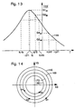
- FIG. 10 represents a curve 144 illustrating the gain
- the filter 116 can be considered as a bandpass filter whose cutoff frequencies are equal to fc-fo and fc + fo.
- Figure 11 illustrates the relationship between the instantaneous values X3 (t) and Y3 (t) of signals X3 and Y3 at an instant t.
- the instantaneous values X3 (t) and Y3 (t) describe a first circle or circle 145 and a second circle or circle 146.
- the radius of the circle 146 is worth + G2 and the radius of circle 145 is + G1.
- the normalization means 118 is arranged to receive the analog signal X3 and, in response, provide a signal representing a standard of the signal X3.
- the conversion means 118 is produced by semiconductor components (achievable in CMOS type technology) so that this standard corresponds to the square function.
- the reference X3 2 designates the signal representing this standard of the signal X3.
- the normalization means 120 is arranged to receive the analog signal Y3 and, in response, to supply a signal representing the same standard of the signal Y3.
- the conversion means 118 is produced by semiconductor components so that this standard corresponds to the square function.
- the reference Y3 2 designates the signal representing this standard of the signal Y3.
- the adder 122 is arranged to receive the signals X3 2 and Y3 2 and, in response, to provide a signal X3 2 + Y3 2 representing the sum of the signals X3 2 and Y3 2 . It is noted that the signal X3 2 + Y3 2 is an analog signal.
- the shaping means 114 is arranged to receive the analog signal X3 2 + Y3 2 and, in response, provide a digital signal Vo equal to a level ⁇ 0 ⁇ (respectively a level ⁇ 1 ⁇ ), when the signal X3 2 + Y3 2 is lower (respectively higher) than a predetermined threshold.
- the shaping means 114 are preferably produced by forming a threshold comparator, this threshold corresponding to the predetermined threshold and being chosen to be between the values + G1 2 and + G2 2 .
- FIG. 12 represents six chronograms 151 to 156.
- the conversion means 3 supplies the signals I and Q so that these signals have sinusoidal waveforms of period T (corresponding to the frequency + ⁇ f1) and in phase quadrature, the signal Q being in advance. on signal I.
- the maximum and minimum amplitudes of the signals I and Q are equal to 1.
- is worth + G2, as has already been described in relation to FIG. 10. It follows that, beyond the instant t0, the values X3 (t) and Y3 (t) of the signals X3 and Y3 describe the circle 146, that is to say that the signals X3 and Y3 have sinusoidal waveforms at the frequency + ⁇ f1 and in phase quadrature, the signal Y3 being ahead of the signal X3.
- the signals X3 and Y3 are proportional to the respective signals I and Q, but behind by a period T1 with respect to the latter, and that they have minimum and maximum amplitudes equal to + G2 and -G2, respectively .
- the normalization means 118 and 120 respectively supply the signals X3 2 and Y3 2 to the summator 122, and the latter supplies in response the signal X3 2 + Y3 2 equal, in this case, to + G2 2 .
- the shaping means 114 supplies in response the signal Vo equal to the level ⁇ 0 ⁇ .
- the complex filter 116 supplies the signals X3 and Y3 so that the gain
- the signals X3 and Y3 are proportional to the signals I and Q, respectively, and have minimum and maximum amplitudes equal to + G1 and -G1.
- the normalization means 118 and 120 respectively supply the signals X3 2 and Y3 2 to the summator 122, and the latter supplies in response the signal X3 2 + Y3 2 equal, in this case, to + G1 2 .
- the shaping means 114 supplies in response the signal Vo equal to the level ⁇ 1 ⁇ .
- the transition between the levels ⁇ 0 ⁇ and ⁇ 1 ⁇ takes place by continuous variations of the signals X3 and Y3 at time t7, as shown in Figure 11.
- the antenna 2 receives a signal at frequency fp + ⁇ f1.
- the situation is similar to that described for time t0. It follows that, beyond the instant t5, the means of setting in form 114 provides in response the signal Vo equal to the level ⁇ 0 ⁇ .
- the antenna 2 receives a signal at frequency fp- ⁇ f1.
- the situation is similar to that described for time t5. It follows that, beyond the instant t7, the means of setting form 114 provides in response the signal Vo equal to the level ⁇ 1 ⁇ .
- the delay T1 between the time when the information is provided by the conversion means 3 and the time when the information is contained in the signal Vo is essentially due to the response time of the complex filter 116, that is to say the response time of the integrators 140 and 142 of this filter.
- This is particularly advantageous, since several pieces of information can thus be received by the antenna 2 and supplied in the form of signal Vo, during the same half-cycle (for example at times t6 and t7).
- the receiver 110 can operate with a low ratio ⁇ f / D (in this example, less than 1), which allows the supply of at least four bits during a period of the signal Vo.
- H3 (jf) an advantage of the transfer function H3 (jf) is to allow a demodulation of the signals I and Q, from an amplitude relation linked to the gain
- receiver 110 can demodulate FSK modulated signals with N frequency jumps designated ⁇ f 1 , ⁇ f 2 , ... ⁇ f N , without structural modification of this receiver (with the exception of the setting means form 114 produced, in this case, by a comparator with N-1 thresholds).
- the values X3 (t) and Y3 (t) can describe a third circle or circle 169 and a fourth circle or circle 170. It is noted that, in the case where the maximum (respectively minimum) amplitudes of the signals I and Q are worth 1 (respectively -1), the radius of the circle 169 is worth G3 and the radius of the circle 170 is worth G4.
- the means for normalizing the receiver according to the present invention can be arranged to provide as standard the function absolue absolute value ⁇ , or function ⁇ power 2m ⁇ , the reference m being an integer greater than or equal to 2.
Abstract
Description
La présente invention concerne le domaine technique des récepteurs pouvant démoduler des signaux électriques et, plus précisément, des récepteurs à conversion directe pour signaux modulés en sauts de fréquence.The present invention relates to the technical field of receivers capable of demodulating electrical signals and, more specifically, direct conversion receivers for frequency hopping modulated signals.
En se référant à la figure 1 de la présente description, le brevet
EP 0.405.676 décrit un récepteur 1 comprenant connectés en série une
antenne 2, un moyen de conversion directe 3, deux amplificateurs limiteurs 28
et 30, un moyen de démodulation 5 et une mémoire bistable 6.Referring to Figure 1 of this description, the patent
EP 0.405.676 describes a
L'antenne 2 reçoit un signal S modulé par sauts de fréquence et fournit
ce signal. Dans la présente description, on rappelle qu'une 〈〈 modulation par
sauts de fréquence 〉〉 dite 〈〈 modulation FSK 〉〉 (acronyme provenant de
l'anglais 〈〈Frequency-Shift Keying 〉〉) est une modulation permettant la
fourniture d'un signal à une fréquence égale à une valeur fp+Δf1 pour
transmettre l'un des deux états du signal, et à une autre valeur fp-Δf1 pour
transmettre l'autre état, les références fp et Δf1 désignant respectivement
une fréquence porteuse nominale et une fréquence de décalage. Pour un débit
de données égal à 512 bits/s, les fréquences fp et Δf1 valent respectivement
400 MHz et 4.5 kHz.The
Le moyen de conversion 3 comprend deux mélangeurs 12 et 14, un
oscillateur local 16, un déphaseur de 90 ° et deux filtres passe-bas 20 et 22.
L'oscillateur 16 fournit une fréquence fL qui est idéalement égale à la
fréquence porteuse fp. Le mélangeur 12 (respectivement 14) comprend une
première borne d'entrée pour recevoir le signal S, une deuxième borne
d'entrée pour recevoir la fréquence fL, et une borne de sortie connecté au
filtre 20 (respectivement 22). En outre, le mélangeur 14 est connecté à
l'oscillateur 16, par l'intermédiaire du déphaseur 18. Il résulte de cet
agencement que, si la fréquence du signal S vaut fp+Δf1, les fréquences
fournies par les mélangeurs 12 et 14 valent respectivement +Δf1 et +Δf1-π/2
et que, si la fréquence du signal S vaut fp-Δf1, les fréquences fournies par les
mélangeurs 12 et 14 valent respectivement -Δf1 et -Δf1-π/2. Le filtre 20
(respectivement 22) peut recevoir la fréquence fournie par le mélangeur 12
(respectivement 14) et, en réponse, fournir un signal I (respectivement un
signal Q). On rappelle que les signaux I et Q représentent les parties réelle et
imaginaire d'un signal complexe ayant une fréquence négative (dans ce cas -
Δf1) ou une fréquence positive (dans ce cas +Δf1). La figure 2 de la présente
description représente deux chronogrammes 24 et 26 illustrant les signaux I
et Q, respectivement. Comme le représente la figure 2, les signaux I et Q sont
des signaux analogiques ayant des formes d'ondes sensiblement sinusoïdales
et en quadrature phase. On note la présence d'un changement de phase du
signal Q, comme l'illustre le chronogramme 26.The conversion means 3 comprises two
En se référant à nouveau à la figure 1, les amplificateurs limiteurs 28 et
30 peuvent recevoir les signaux I et Q et, en réponse, fournir des signaux I1 et
Q1, respectivement. On rappelle qu'un amplificateur limiteur reçoit un signal
d'entrée, et fournit un signal de sortie dont l'amplitude n'augmente
pratiquement plus au-delà d'une amplitude déterminée du signal d'entrée. La
figure 3A de la présente description représente deux chronogrammes 32 et
34 illustrant les signaux I1 et Q1, respectivement. Comme le représente la
figure 3A, les signaux I1 et Q1 sont des signaux numériques ayant des formes
d'ondes décalées l'une de l'autre et rectangulaires, les amplitudes des signaux
I1 et Q1 valant -1 ou +1.Referring again to FIG. 1, the
La figure 3B représente une courbe 80 illustrant la relation entre les
valeurs instantanées I1(t) et Q1(t) des signaux I1 et Q1 à un instant t.
Comme le représente la figure 3B, la courbe 80 a une forme rectangulaire
dont les sommets sont formés par quatre points A à D. On note qu'une
évolution temporelle de ces signaux se traduit par un parcours le long de
cette courbe, de sorte que, quand le signal Vout vaut 0 (respectivement 1),
les signaux I1 et Q1 sont représentés successivement par les points A, B, C,
D, A... (respectivement A, D, C, B, A...), c'est-à-dire un parcours selon le sens
trigonométrique (respectivement selon le sens inverse au sens
trigonométrique).FIG. 3B represents a
En se référant à nouveau à la figure 1, le moyen de démodulation 5
comprend connectés en série un circuit différentiateur 40 (respectivement
42), un multiplicateur 36 (respectivement 38) et un soustracteur 39.Referring again to FIG. 1, the demodulation means 5
comprises connected in series a differentiator circuit 40 (respectively
42), a multiplier 36 (respectively 38) and a
Le multiplicateur 36 (respectivement 38) comprend une première borne
d'entrée pour recevoir le signal Q1 (respectivement I1), et une deuxième
borne d'entrée pour recevoir le signal I1 (respectivement Q1), par
l'intermédiaire du circuit différentiateur 40 (respectivement 42). Le
multiplicateur 36 (respectivement 38) est agencé pour fournir le signal X1
(respectivement Y1). La figure 4 de la présente description représente deux
chronogrammes 44 et 46 illustrant les signaux X1 et Y1, respectivement.
Comme le représente la figure 4, le signal X1 contient des premières
impulsions, et le signal Y1 contient des deuxièmes impulsions décalées par
rapport aux premières impulsions. Le soustracteur 39 comprend une
première borne d'entrée pour recevoir le signal X1 et une deuxième borne
d'entrée pour recevoir le signal Y1. Le soustracteur 39 est agencé pour
fournir un signal X1-Y1 égal à la différence entre les signaux X1 et Y1. La
figure 5 de la présente description représente un chronogramme 48 illustrant
le signal X1-Y1. Comme le représente la figure 5, le signal X1-Y1 contient les
impulsions résultant de la différence entre les signaux X1 et Y1. On note que,
avant le changement de phase du signal Q, le signal X1-Y1 contient des
impulsions négatives et que ce changement de phase provoque la fourniture
d'impulsions positives.The multiplier 36 (respectively 38) comprises a first terminal
input to receive signal Q1 (respectively I1), and a second
input terminal to receive the signal I1 (respectively Q1), by
through the differentiating circuit 40 (respectively 42). The
multiplier 36 (respectively 38) is arranged to supply the signal X1
(respectively Y1). Figure 4 of this description shows two
timing diagrams 44 and 46 illustrating the signals X1 and Y1, respectively.
As shown in Figure 4, the signal X1 contains first
pulses, and signal Y1 contains second pulses offset by
compared to the first pulses.
La mémoire bistable 6 comprend une borne d'entrée pour recevoir le
signal X1-Y1, et une borne de sortie pour fournir en réponse un signal Vout.
La figure 6 de la présente description représente un chronogramme 50
illustrant le signal Vout. Comme le représente la figure 6, le signal Vout est
égal à un niveau 〈〈 0 〉〉 ou à un niveau 〈〈 1 〉〉. On note que, dès qu'une
impulsion positive apparaít sur le signal X1-Y1 le signal Vout commute du
niveau 〈〈 0 〉〉 au niveau 〈〈 1 〉〉, et demeure à ce niveau, indépendamment de la
différence ultérieure de fréquences entre les signaux X1 et Y1.The
On va maintenant décrire brièvement le fonctionnement du récepteur 1,
à l'aide des figures 1 à 6 déjà citées.We will now briefly describe the operation of
Jusqu'à un instant t01, les signaux I1 et Q1 sont périodiques de période
T, le signal I1 étant en avance sur le signal Q1, de sorte que le signal Vout
vaut 0. Les signaux I1 et Q1 sont représentés successivement par les points
A, B, C, D, A... Ainsi, à l'instant t01, le signal Q1 devient égal à 1. A un instant
t1 ultérieur à l'instant t01 et antérieur à un instant t01+T/2, une nouvelle
information est présente dans le signal Q, de sorte que la temporisation des
signaux I1 et Q1 est inversée au-delà de l'instant t01+T/2 (c'est-à-dire les
signaux I1 et Q1 sont représentés successivement par les points B, A, D, C,
B...). On note que la commutation du signal Vout a lieu lors de la commutation
suivante du signal I1 au niveau 〈〈 -1 〉〉, c'est-à-dire à un instant t3. Autrement
dit, il existe un retard entre l'instant où l'information est contenue dans le
signal Q (c'est-à-dire l'instant t1) et l'instant où l'information est contenue
dans le signal Vout (c'est-à-dire l'instant t3). On note que ce retard est
compris entre T/2 et T, ce qui nécessite un rapport Δf/D élevé, la référence
Δf désignant la fréquence de décalage (égale dans ce cas à Df1) et la
référence D désignant le débit binaire. Ainsi un inconvénient du récepteur 1 est
d'avoir un rapport Δf/D élevé : un bit est typiquement fourni toutes les quatre
périodes.Up to an instant t01, the signals I1 and Q1 are periodical
T, the signal I1 being ahead of the signal Q1, so that the signal Vout
is worth 0. The signals I1 and Q1 are represented successively by the points
A, B, C, D, A ... Thus, at time t01, the signal Q1 becomes equal to 1. At a time
t1 subsequent to time t01 and prior to time t01 + T / 2, a new
information is present in the Q signal, so the timing of
signals I1 and Q1 is reversed beyond time t01 + T / 2 (i.e. the
signals I1 and Q1 are represented successively by points B, A, D, C,
B ...). It is noted that the switching of the signal Vout takes place during the switching
next to signal I1 at level 〈〈 -1 〉〉, that is to say at time t3. Other
says there is a delay between the time the information is contained in the
signal Q (i.e. time t1) and the time when the information is contained
in the signal Vout (that is to say the instant t3). We note that this delay is
between T / 2 and T, which requires a high Δf / D ratio, the reference
Δf denoting the offset frequency (equal in this case to Df1) and the
reference D designating the bit rate. So a drawback of
Pour pallier un tel inconvénient, il existe dans l'état de la technique des récepteurs de signaux modulés FSK réalisant une démodulation directement à partir des signaux analogiques I et Q fournis par le moyen de conversion.To overcome such a drawback, there are in the state of the art FSK modulated signal receivers demodulating directly at starting from the analog signals I and Q supplied by the conversion means.
En se référant à la figure 7 de la présente description, le brevet
US 5.640.428 décrit un récepteur 90 comprenant une antenne 2, un moyen
de conversion 3, un moyen de démodulation 92 et un filtre passe-bas 94. On
note que des objets de la figure 7 similaires à ceux décrits en relation avec la
figure 1 ont été désignés par les mêmes références. Comme le représente la
figure 7, le moyen de démodulation 92 comprend quatre mélangeurs 96 à 99,
deux circuits de maintien 100 et 101 et trois circuits à retard 102 à 104. On
note que le récepteur 90 réalise une démodulation d'un signal S reçu par
l'antenne 2, par un traitement analogique de ce signal. Toutefois ce
traitement est réalisé par des éléments de traitement numérique (signaux
d'horloge, bascules), à l'instar du récepteur 1 de la figure 1.Referring to Figure 7 of this description, the patent
US 5,640,428 describes a
En outre, un inconvénient des récepteurs 1 et 90 est que les moyens de
démodulation 5 et 92 contiennent des multiplicateurs qui sont des
composants ayant une structure complexe (notamment deux bornes
d'entrée) c'est-à-dire des composants difficiles à fabriquer.In addition, a drawback of
Un objet de la présente invention est de prévoir un récepteur de signaux modulés FSK palliant les inconvénients susmentionnés, notamment un tel récepteur réalisant une démodulation instantanée sur la base de signaux analogiques.An object of the present invention is to provide a receiver for FSK modulated signals overcoming the aforementioned drawbacks, in particular a such receiver performing instant demodulation on the basis of signals analog.
Un autre objet de la présente invention est de prévoir un récepteur de signaux modulés FSK réalisant la démodulation d'informations reçues avec un rapport Δf/D minimum (typiquement inférieur à 1).Another object of the present invention is to provide a receiver for FSK modulated signals demodulating information received with a minimum Δf / D ratio (typically less than 1).
Un autre objet de la présente invention est de prévoir un récepteur de signaux modulés FSK comprenant un moyen de démodulation dépourvu de multiplicateurs.Another object of the present invention is to provide a receiver for FSK modulated signals comprising a demodulation means devoid of multipliers.
Un autre objet de la présente invention est de prévoir un récepteur de signaux modulés FSK répondant aux critères de rationalité, d'encombrement et de coût, qui sont traditionnels dans l'industrie des semi-conducteurs.Another object of the present invention is to provide a receiver for FSK modulated signals meeting the criteria of rationality, congestion and cost, which are traditional in the semiconductor industry.
Ces objets, ainsi que d'autres, sont atteints par le récepteur selon la
revendication 1.These and other objects are reached by the receiver according to the
Un avantage du filtre complexe d'un tel récepteur est de pouvoir être réalisé par des composants semiconducteurs simples à fabriquer, sans former de multiplicateurs ou de mélangeurs à plusieurs entrées, à l'instar des récepteurs classiques.An advantage of the complex filter of such a receiver is that it can be made of semiconductor components that are simple to manufacture, without train multipliers or mixers with several inputs, like conventional receivers.
Un autre avantage du filtre d'un tel récepteur est de filtrer la moitié du bruit provenant du signal modulé, ce qui diminue notablement l'influence du bruit sur le signal de sortie du récepteur.Another advantage of the filter of such a receiver is to filter half of the noise from the modulated signal, which significantly reduces the influence of noise on the receiver output signal.
Ces objets, caractéristiques et avantages, ainsi que d'autres, de la présente invention apparaítront plus clairement à la lecture de la description détaillée d'un mode de réalisation préféré de l'invention, donné à titre d'exemple uniquement, en relation avec les figures jointes, parmi lesquelles :
- la figure 1 déjà citée représente un premier récepteur classique;
- les figures 2, 3A et 4 déjà citées représentent chacune deux chronogrammes illustrant des signaux électriques présents dans le récepteur de la figure 1;
- la figure 3B déjà citée représente une courbe illustrant la relation entre les deux signaux électriques de la figure 3A;
- les figures 5 et 6 déjà citées représentent chacune un chronogramme illustrant un signal électrique présent dans le récepteur de la figure 1;
- la figure 7 déjà citée représente un deuxième récepteur classique;
- la figure 8 représente un récepteur selon la présente invention;
- la figure 9 représente un mode réalisation d'un filtre du récepteur de la figure 8;
- la figure 10 représente une courbe illustrant le gain du filtre de la figure 9, en relation avec une modulation à deux sauts de fréquence;
- la figure 11 représente une courbe illustrant la relation entre deux signaux électriques fournis par le filtre de la figure 9, en relation avec une modulation à deux sauts de fréquence;
- la figure 12 représente dix chronogrammes illustrant des signaux électriques présents dans le récepteur de la figure 8;
- la figure 13 représente une courbe illustrant le gain du filtre de la figure 9, en relation avec une modulation à quatre sauts de fréquences; et
- la figure 14 représente une courbe illustrant la relation entre deux signaux électriques fournis par le filtre de la figure 9, en relation avec une modulation à quatre sauts de fréquences.
- Figure 1 already cited shows a first conventional receiver;
- Figures 2, 3A and 4 already cited each represent two timing diagrams illustrating electrical signals present in the receiver of Figure 1;
- FIG. 3B, already cited, represents a curve illustrating the relationship between the two electrical signals of FIG. 3A;
- Figures 5 and 6 already cited each represent a timing diagram illustrating an electrical signal present in the receiver of Figure 1;
- Figure 7 already cited shows a second conventional receiver;
- Figure 8 shows a receiver according to the present invention;
- FIG. 9 represents an embodiment of a filter of the receiver of FIG. 8;
- FIG. 10 represents a curve illustrating the gain of the filter of FIG. 9, in relation to a modulation with two frequency jumps;
- FIG. 11 represents a curve illustrating the relationship between two electrical signals supplied by the filter of FIG. 9, in relation to a modulation with two frequency hops;
- Figure 12 shows ten timing diagrams illustrating electrical signals present in the receiver of Figure 8;
- FIG. 13 represents a curve illustrating the gain of the filter of FIG. 9, in relation to a modulation with four frequency hops; and
- FIG. 14 represents a curve illustrating the relationship between two electrical signals supplied by the filter of FIG. 9, in relation to a modulation with four frequency hops.
La figure 8 représente un récepteur 110 selon la présente invention
comprenant une antenne 2, un moyen de conversion 3, un moyen de
démodulation 112 et un moyen de mise en forme 114. Comme le représente
la figure 8, le moyen de démodulation 112 comprend un filtre complexe 116,
deux moyens de normalisation 118 et 120 et un sommateur 122.FIG. 8 represents a
On note que des objets de la figure 8 similaires à ceux décrits en
relation avec la figure 1 ont été désignés par les mêmes références. Toutefois
les filtres 20 et 23 du moyen de conversion 3 tel que décrit en relation avec la
figure 1 ne sont pas nécessaires à la réalisation du récepteur 110, la fonction
de ces filtres étant assurée par le filtre complexe 116.Note that objects in Figure 8 similar to those described in
relationship with Figure 1 have been designated by the same references. However
the
Le filtre complexe 116 est agencé pour recevoir les signaux analogiques
I et Q fournis par le moyen de conversion 3, comme cela a déjà été décrit de
façon plus détaillée en relation avec la figure 1. Le filtre complexe 116 est
également agencé pour fournir deux signaux analogiques X3 et Y3 de sorte
que les signaux I, Q, X3 et Y3 sont liées par la relation suivante :
La figure 9 représente un mode réalisation du filtre complexe 116
comprenant deux sommateurs 124 et 126, six amplificateurs 128, 130, 132,
134, 136 et 138, et deux intégrateurs 140 et 142. On note que les gains des
amplificateurs 128 et 130 valent fo, que ceux des amplificateurs 132 et 134
valent -1 et que ceux des amplificateurs 136 et 138 valent -fc/fo.FIG. 9 represents an embodiment of the
Le sommateur 124, l'intégrateur 140 et l'amplificateur 128 sont
connectés en série, et agencés de sorte que le sommateur 124 reçoit le signal
analogique I et que l'amplificateur 128 fournit le signal X3. Le sommateur 124
reçoit également le signal X3 par l'intermédiaire de l'amplificateur 132. De
même, le sommateur 126, l'intégrateur 142 et l'amplificateur 130 sont
connectés en série, et agencés de sorte que le sommateur 126 reçoit le signal
analogique Q et que l'amplificateur 130 fournit le signal Y3. Le sommateur
126 reçoit également le signal Y3 par l'intermédiaire de l'amplificateur 134. En
outre, le sommateur 124 reçoit également le signal Y3 par l'intermédiaire de
l'amplificateur 136, et le sommateur 126 reçoit également le signal X3 par
l'intermédiaire de l'amplificateur 138. The
On réalise de préférence le moyen de conversion 3 et le moyen de
démodulation 112 en formant des composants (réalisables par une
technologie de type CMOS), de sorte que les amplitudes des signaux X3 et Y3
sont égales. A titre de perfectionnement, le récepteur 110 peut comprendre
deux amplificateurs à gain variable (connus en soi) connectés de sorte que le
moyen de conversion 3 fournit au moyen de démodulation 112 le signal I
(respectivement le signal Q), par l'intermédiaire de l'un de ces amplificateurs
(respectivement de l'autre de ces amplificateurs).Preferably, the conversion means 3 and the means of
La figure 10 représente une courbe 144 illustrant le gain |H3(jf)| relatif
au filtre 161 tel que représenté en figure 9. On note en figure 10 que le gain
|H3(jf)| est représenté selon une échelle logarithmique, et que la fréquence f
est représentée selon une échelle linéaire. La courbe 144 est centrée sur la
fréquence fc, de sorte que la fonction de transfert H3(jf) est asymétrique.
L'homme du métier note que le filtre 116 peut être considéré comme un filtre
passe-bande dont les fréquences de coupure valent fc-fo et fc+fo. On note
qu'il résulte de l'asymétrie de cette fonction de transfert que le gain |H3(jf)|
vaut +G1 quand la fréquence f vaut -Δf1, que le gain |H3(jf)| vaut +G2 quand
la fréquence f vaut +Δf1, et que
La figure 11 illustre la relation entre les valeurs instantanées X3(t) et
Y3(t) des signaux X3 et Y3 à un instant t. Comme le représente la figure 11,
au cours du temps t, les valeurs instantanées X3(t) et Y3(t) décrivent un
premier cercle ou cercle 145 et un deuxième cercle ou cercle 146. On note
que, dans le cas où les amplitudes maximales (respectivement minimales) des
signaux I et Q valent 1 (respectivement -1), le rayon du cercle 146 vaut +G2
et le rayon du cercle 145 vaut +G1. On notera qu'une évolution temporelle de
ces signaux se traduit par un parcours le long de ces cercles, de sorte que,
quand les signaux X3 et Y3 décrivent le cercle 146 (respectivement le cercle
145) selon le sens trigonométrique (respectivement selon le sens inverse au
sens trigonométrique), le signal Vout vaut 0 (respectivement 1).Figure 11 illustrates the relationship between the instantaneous values X3 (t) and
Y3 (t) of signals X3 and Y3 at an instant t. As shown in Figure 11,
during time t, the instantaneous values X3 (t) and Y3 (t) describe a
first circle or
En se référant à nouveau à la figure 8, le moyen de normalisation 118 est agencé pour recevoir le signal analogique X3 et, en réponse, fournir un signal représentant une norme du signal X3. De préférence, on réalise le moyen de conversion 118 par des composants semiconducteurs (réalisables en technologie de type CMOS) de sorte que cette norme correspond à la fonction carrée. Ainsi, à titre illustratif uniquement, dans la suite de la description, la référence X32 désigne le signal représentant cette norme du signal X3.Referring again to Figure 8, the normalization means 118 is arranged to receive the analog signal X3 and, in response, provide a signal representing a standard of the signal X3. Preferably, the conversion means 118 is produced by semiconductor components (achievable in CMOS type technology) so that this standard corresponds to the square function. Thus, by way of illustration only, in the following description, the reference X3 2 designates the signal representing this standard of the signal X3.
De même, le moyen de normalisation 120 est agencé pour recevoir le signal analogique Y3 et, en réponse, fournir un signal représentant la même norme du signal Y3. De préférence, on réalise le moyen de conversion 118 par des composants semiconducteurs de sorte que cette norme correspond à la fonction carrée. Ainsi, à titre illustratif uniquement, dans la suite de la description, la référence Y32 désigne le signal représentant cette norme du signal Y3.Likewise, the normalization means 120 is arranged to receive the analog signal Y3 and, in response, to supply a signal representing the same standard of the signal Y3. Preferably, the conversion means 118 is produced by semiconductor components so that this standard corresponds to the square function. Thus, by way of illustration only, in the following description, the reference Y3 2 designates the signal representing this standard of the signal Y3.
Le sommateur 122 est agencé pour recevoir les signaux X32 et Y32 et,
en réponse, pour fournir un signal X32+Y32 représentant la somme des
signaux X32 et Y32. On note que le signal X32+Y32 est un signal analogique.The
En se référant à nouveau à la figure 8, le moyen de mise en forme 114 est agencé pour recevoir le signal analogique X32+Y32 et, en réponse, fournir un signal numérique Vo égale à un niveau 〈〈 0 〉〉 (respectivement un niveau 〈〈 1 〉〉), quand le signal X32+Y32 est inférieur (respectivement supérieur) à un seuil prédéterminé. On réalise de préférence le moyen de mise en forme 114 en formant un comparateur à seuil, ce seuil correspondant au seuil prédéterminé et étant choisi pour être compris entre les valeurs +G12 et +G22.Referring again to Figure 8, the shaping means 114 is arranged to receive the analog signal X3 2 + Y3 2 and, in response, provide a digital signal Vo equal to a level 〈〈 0 〉〉 (respectively a level 〈〈 1 〉〉), when the signal X3 2 + Y3 2 is lower (respectively higher) than a predetermined threshold. The shaping means 114 are preferably produced by forming a threshold comparator, this threshold corresponding to the predetermined threshold and being chosen to be between the values + G1 2 and + G2 2 .
On va maintenant décrire le fonctionnement du récepteur 110 à l'aide
de la figure 12 qui représente six chronogrammes 151 à 156.We will now describe the operation of the
Considérons à un instant initial t0 que l'antenne 2 reçoit un signal à la
fréquence fp+Δf1 . Il en résulte que le moyen de conversion 3 fournit les
signaux I et Q de sorte que ces signaux ont des formes d'onde sinusoïdales
de période T (correspondant à la fréquence +Δf1) et en quadrature de
phase, le signal Q étant en avance sur le signal I. A titre d'exemple, on
suppose que les amplitudes maximales et minimales des signaux I et Q vaut 1.
Le filtre complexe 116 reçoit ces signaux I et Q et fournit en réponse les
signaux X3 et Y3 de sorte que :
Considérons à un instant t5 ultérieur à l'instant t0 que l'antenne 2
reçoit un signal à la fréquence fp-Δf1, ce qui provoque une modification de la
forme d'onde du signal Q fourni par le moyen de conversion 3. En réponse, le
filtre complexe 116 fournit les signaux X3 et Y3 de sorte que le gain |H3(jf)|
vaut +G1, étant donné que la fréquence f des signaux I et Q vaut -Δf1. Il en
résulte que, au-delà de l'instant t5, les valeurs X3(t) et Y3(t) des signaux X3
et Y3 décrivent le cercle 145, c'est-à-dire que les signaux X3 et Y3 ont des
formes d'onde sinusoïdales à la fréquence -Δf1 et en quadrature de phase. On
note que les signaux X3 et Y3 sont proportionnels aux signaux I et Q,
respectivement, et ont des amplitudes minimales et maximales égales à +G1
et -G1. Ainsi, au-delà de l'instant t5, les moyens de normalisation 118 et 120
fournissent respectivement les signaux X32 et Y32 au sommateur 122, et ce
dernier fournit en réponse le signal X32+Y32 égal, dans ce cas, à +G12. Et le
moyen de mise en forme 114 fournit en réponse le signal Vo égal au niveau
〈〈 1 〉〉. On note que la transition entre les niveaux 〈〈 0 〉〉 et 〈〈 1 〉〉 a lieu par
des variations continues des signaux X3 et Y3 à l'instant t7, comme le
représente la figure 11.Consider at a time t5 subsequent to time t0 that the
De même, à un instant t6 ultérieur à l'instant t5, l'antenne 2 reçoit un
signal à la fréquence fp+Δf1. La situation est similaire à celle décrite pour
l'instant t0. Il en résulte que, au-delà de l'instant t5, le moyen de mise en
forme 114 fournit en réponse le signal Vo égal au niveau 〈〈 0 〉〉.Likewise, at a time t6 subsequent to time t5, the
De même, à un instant t7 ultérieur à l'instant t6, l'antenne 2 reçoit un
signal à la fréquence fp-Δf1. La situation est similaire à celle décrite pour
l'instant t5. Il en résulte que, au-delà de l'instant t7, le moyen de mise en
forme 114 fournit en réponse le signal Vo égal au niveau 〈〈 1 〉〉.Likewise, at a time t7 subsequent to time t6, the
On note que, à l'instant où les signaux I et Q contiennent une
information (-Δf1 ou +Δf1) provenant de l'antenne 2, cette information est
fournie au même instant au moyen de démodulation 112, contrairement au
récepteur classique 1 dans lequel l'information n'est fournie au moyen de
conversion 5 qu'au demi-cycle suivant (occasionnant un retard égal à T/2, la
référence T désignant la période des signaux I1 et Q1, comme cela a été
décrit en relation avec les figures 1 à 6).We note that, at the moment when the signals I and Q contain a
information (-Δf1 or + Δf1) from
On note également que le retard T1 entre l'instant où l'information est
fournie par le moyen de conversion 3 et l'instant où l'information est contenue
dans le signal Vo est essentiellement dû au temps de réponse du filtre,
complexe 116, c'est-à-dire au temps de réponse des intégrateurs 140 et 142
de ce filtre. Ceci est particulièrement avantageux, puisque que plusieurs
informations peuvent ainsi être reçues par l'antenne 2 et fournies sous la
forme de signal Vo, au cours d'un même demi-cycle (par exemple aux instants
t6 et t7). Il en ressort que le récepteur 110 peut fonctionner avec un faible
rapport Δf/D (dans cet exemple, inférieur à 1), ce qui permet la fourniture
d'au moins quatre bits au cours d'une période du signal Vo. On note
également qu'un avantage de la fonction de transfert H3(jf) est de permettre
une démodulation des signaux I et Q, à partir d'une relation d'amplitude liée
au gain |H3(jf)|, puisque :
Un autre avantage du récepteur 110 est de pouvoir réaliser une
démodulation de signaux modulés FSK avec N sauts de fréquence désignés
Δf1, Δf2,... ΔfN, sans modification structurelle de ce récepteur (à l'exception du
moyen de mise en forme 114 réalisé, dans ce cas, par un comparateur à N-1
seuils).Another advantage of the
En effet, considérons le cas où N=4 et plus particulièrement le cas où
Il va de soi pour l'homme de l'art que la description détaillée ci-dessus peut subir diverses modifications sans sortir du cadre de la présente invention. A titre d'exemple, les moyens de normalisation du récepteur selon la présente invention peuvent être agencés pour fournir en tant que norme la fonction 〈〈 valeur absolue 〉〉, ou la fonction 〈〈 puissance 2m 〉〉, la référence m étant un nombre entier supérieur ou égal à 2.It goes without saying for those skilled in the art that the detailed description above may undergo various modifications without departing from the scope of this invention. By way of example, the means for normalizing the receiver according to the present invention can be arranged to provide as standard the function absolue absolute value 〉〉, or function 〈〈 power 2m 〉〉, the reference m being an integer greater than or equal to 2.
Claims (7)
Priority Applications (4)
| Application Number | Priority Date | Filing Date | Title |
|---|---|---|---|
| EP98124582A EP1014637B1 (en) | 1998-12-23 | 1998-12-23 | Direct conversion receiver for FSK modulated signals |
| DE69834407T DE69834407T2 (en) | 1998-12-23 | 1998-12-23 | Direct mix receiver for FSK modulated signals |
| US09/466,892 US6563887B1 (en) | 1998-12-23 | 1999-12-20 | Direct conversion receiver for frequency-shift keying modulated signals |
| JP36691099A JP4267786B2 (en) | 1998-12-23 | 1999-12-24 | Direct conversion receiver for frequency shift keyed signals |
Applications Claiming Priority (1)
| Application Number | Priority Date | Filing Date | Title |
|---|---|---|---|
| EP98124582A EP1014637B1 (en) | 1998-12-23 | 1998-12-23 | Direct conversion receiver for FSK modulated signals |
Publications (2)
| Publication Number | Publication Date |
|---|---|
| EP1014637A1 true EP1014637A1 (en) | 2000-06-28 |
| EP1014637B1 EP1014637B1 (en) | 2006-05-03 |
Family
ID=8233236
Family Applications (1)
| Application Number | Title | Priority Date | Filing Date |
|---|---|---|---|
| EP98124582A Expired - Lifetime EP1014637B1 (en) | 1998-12-23 | 1998-12-23 | Direct conversion receiver for FSK modulated signals |
Country Status (4)
| Country | Link |
|---|---|
| US (1) | US6563887B1 (en) |
| EP (1) | EP1014637B1 (en) |
| JP (1) | JP4267786B2 (en) |
| DE (1) | DE69834407T2 (en) |
Families Citing this family (2)
| Publication number | Priority date | Publication date | Assignee | Title |
|---|---|---|---|---|
| JP4063563B2 (en) * | 2002-03-25 | 2008-03-19 | 株式会社日立国際電気 | Direct detection circuit |
| US7146148B2 (en) * | 2002-10-01 | 2006-12-05 | Hitachi Kokusai Electric Inc. | Low intermediate frequency type receiver |
Citations (4)
| Publication number | Priority date | Publication date | Assignee | Title |
|---|---|---|---|---|
| US4437068A (en) * | 1981-02-19 | 1984-03-13 | Thomson-Csf | FSK Demodulator for frequency-modulation modem |
| EP0305125A1 (en) * | 1987-08-21 | 1989-03-01 | BRITISH TELECOMMUNICATIONS public limited company | FSK discriminator |
| EP0405676A2 (en) * | 1989-06-30 | 1991-01-02 | Philips Electronics Uk Limited | Direct-conversion FSK receiver having a DC output independent of frequency drift |
| US5640428A (en) * | 1994-11-10 | 1997-06-17 | Matsushita Electric Industrial Co, Ltd. | Direct conversion receiver |
Family Cites Families (6)
| Publication number | Priority date | Publication date | Assignee | Title |
|---|---|---|---|---|
| GB2149244B (en) * | 1983-10-29 | 1987-01-21 | Standard Telephones Cables Ltd | Digital demodulator arrangement for quadrature signals |
| US5249203A (en) * | 1991-02-25 | 1993-09-28 | Rockwell International Corporation | Phase and gain error control system for use in an i/q direct conversion receiver |
| US5828705A (en) * | 1996-02-01 | 1998-10-27 | Kroeger; Brian W. | Carrier tracking technique and apparatus having automatic flywheel/tracking/reacquisition control and extended signal to noise ratio |
| US5937341A (en) * | 1996-09-13 | 1999-08-10 | University Of Washington | Simplified high frequency tuner and tuning method |
| EP0948128B1 (en) * | 1998-04-03 | 2004-12-01 | Motorola Semiconducteurs S.A. | DC offset cancellation in a quadrature receiver |
| US6304751B1 (en) * | 1998-12-29 | 2001-10-16 | Cirrus Logic, Inc. | Circuits, systems and methods for digital correction of phase and magnitude errors in image reject mixers |
-
1998
- 1998-12-23 DE DE69834407T patent/DE69834407T2/en not_active Expired - Lifetime
- 1998-12-23 EP EP98124582A patent/EP1014637B1/en not_active Expired - Lifetime
-
1999
- 1999-12-20 US US09/466,892 patent/US6563887B1/en not_active Expired - Lifetime
- 1999-12-24 JP JP36691099A patent/JP4267786B2/en not_active Expired - Fee Related
Patent Citations (4)
| Publication number | Priority date | Publication date | Assignee | Title |
|---|---|---|---|---|
| US4437068A (en) * | 1981-02-19 | 1984-03-13 | Thomson-Csf | FSK Demodulator for frequency-modulation modem |
| EP0305125A1 (en) * | 1987-08-21 | 1989-03-01 | BRITISH TELECOMMUNICATIONS public limited company | FSK discriminator |
| EP0405676A2 (en) * | 1989-06-30 | 1991-01-02 | Philips Electronics Uk Limited | Direct-conversion FSK receiver having a DC output independent of frequency drift |
| US5640428A (en) * | 1994-11-10 | 1997-06-17 | Matsushita Electric Industrial Co, Ltd. | Direct conversion receiver |
Also Published As
| Publication number | Publication date |
|---|---|
| EP1014637B1 (en) | 2006-05-03 |
| DE69834407T2 (en) | 2007-04-19 |
| JP2000196685A (en) | 2000-07-14 |
| US6563887B1 (en) | 2003-05-13 |
| DE69834407D1 (en) | 2006-06-08 |
| JP4267786B2 (en) | 2009-05-27 |
Similar Documents
| Publication | Publication Date | Title |
|---|---|---|
| EP0530107B1 (en) | PSK demodulator with baseband correction for phase or frequency errors | |
| FR2494059A1 (en) | QUICK ACQUISITION CARRIER DEMODULATION METHOD AND DEVICE | |
| EP0451232B1 (en) | Code acquisition method and circuit for a spread spectrum signal receiver | |
| EP0125979B1 (en) | Demodulator for constant envelope and continuous phase signals angularly modulated by a series of binary symbols | |
| EP0209928B1 (en) | Demodulator for a frequency-modulated digital signal | |
| FR2662890A1 (en) | DIGITAL DEMODULATOR FOR MULTIPURPOSE PHASE DISPLACEMENT MODULE SIGNAL. | |
| EP0635946B1 (en) | Analog to digital converter with modulated feedback | |
| EP1014637B1 (en) | Direct conversion receiver for FSK modulated signals | |
| FR2551279A1 (en) | SINUSOIDAL WAVE GENERATOR, OF WHICH FREQUENCY IS SUBJECT TO A BINARY SIGNAL, PARTICULARLY FOR MODEM | |
| FR2669786A1 (en) | DOUBLE FREQUENCY DEVICE. | |
| EP3116182B1 (en) | Quadrature demodulator for very high throughput rfid receiver | |
| EP0092474B1 (en) | Demodulation filter for a binary frequency-modulated signal | |
| EP1514352B1 (en) | Delay-locked loop | |
| EP0021943B1 (en) | Microwave digital data transmission system | |
| EP0031762A2 (en) | Modulator-demodulator for transmission by a four-level double amplitude modulation on quadrature carriers | |
| EP0225218A1 (en) | Frequency synthesis method and synthesis apparatus using this method | |
| FR2595895A1 (en) | DOUBLE DIGITAL DEMODULATOR | |
| FR2700228A1 (en) | Phase-shaping device for each of the packets of a phase modulated digital signal, and corresponding receiver. | |
| EP0035434B1 (en) | Transmitting and receiving device for the transmission of digital signals | |
| WO2018115139A2 (en) | Device for generating a modulated digital signal and system for generating a modulated analog signal | |
| US7382846B1 (en) | Off-symbol correlation technique | |
| FR2717971A1 (en) | Device for synthesizing a signal form, transmitter station and receiver station comprising such a device. | |
| FR2633127A1 (en) | Method of modulating a single side band signal and modulator by which the method is implemented | |
| WO2001078226A1 (en) | Circuit and method for generating phase-shifted signals | |
| FR3084803A1 (en) | DEMODULATOR AND DEMODULATION METHOD |
Legal Events
| Date | Code | Title | Description |
|---|---|---|---|
| PUAI | Public reference made under article 153(3) epc to a published international application that has entered the european phase |
Free format text: ORIGINAL CODE: 0009012 |
|
| AK | Designated contracting states |
Kind code of ref document: A1 Designated state(s): CH DE FR GB IT LI NL |
|
| AX | Request for extension of the european patent |
Free format text: AL;LT;LV;MK;RO;SI |
|
| 17P | Request for examination filed |
Effective date: 20001228 |
|
| AKX | Designation fees paid |
Free format text: CH DE FR GB IT LI NL |
|
| GRAP | Despatch of communication of intention to grant a patent |
Free format text: ORIGINAL CODE: EPIDOSNIGR1 |
|
| GRAS | Grant fee paid |
Free format text: ORIGINAL CODE: EPIDOSNIGR3 |
|
| GRAA | (expected) grant |
Free format text: ORIGINAL CODE: 0009210 |
|
| AK | Designated contracting states |
Kind code of ref document: B1 Designated state(s): CH DE FR GB IT LI NL |
|
| PG25 | Lapsed in a contracting state [announced via postgrant information from national office to epo] |
Ref country code: IT Free format text: LAPSE BECAUSE OF FAILURE TO SUBMIT A TRANSLATION OF THE DESCRIPTION OR TO PAY THE FEE WITHIN THE PRESCRIBED TIME-LIMIT;WARNING: LAPSES OF ITALIAN PATENTS WITH EFFECTIVE DATE BEFORE 2007 MAY HAVE OCCURRED AT ANY TIME BEFORE 2007. THE CORRECT EFFECTIVE DATE MAY BE DIFFERENT FROM THE ONE RECORDED. Effective date: 20060503 |
|
| REG | Reference to a national code |
Ref country code: GB Ref legal event code: FG4D Free format text: NOT ENGLISH |
|
| REG | Reference to a national code |
Ref country code: CH Ref legal event code: EP |
|
| REF | Corresponds to: |
Ref document number: 69834407 Country of ref document: DE Date of ref document: 20060608 Kind code of ref document: P |
|
| REG | Reference to a national code |
Ref country code: CH Ref legal event code: NV Representative=s name: ICB INGENIEURS CONSEILS EN BREVETS SA |
|
| RAP2 | Party data changed (patent owner data changed or rights of a patent transferred) |
Owner name: ASULAB S.A. |
|
| GBT | Gb: translation of ep patent filed (gb section 77(6)(a)/1977) |
Effective date: 20060911 |
|
| NLT2 | Nl: modifications (of names), taken from the european patent patent bulletin |
Owner name: ASULAB S.A. Effective date: 20060906 |
|
| PLBE | No opposition filed within time limit |
Free format text: ORIGINAL CODE: 0009261 |
|
| STAA | Information on the status of an ep patent application or granted ep patent |
Free format text: STATUS: NO OPPOSITION FILED WITHIN TIME LIMIT |
|
| 26N | No opposition filed |
Effective date: 20070206 |
|
| REG | Reference to a national code |
Ref country code: CH Ref legal event code: PFA Owner name: ASULAB S.A. Free format text: ASULAB S.A.#FAUBOURG DU LAC 6#CH-2501 BIENNE (CH) -TRANSFER TO- ASULAB S.A.#RUE DES SORS 3#2074 MARIN (CH) |
|
| PGFP | Annual fee paid to national office [announced via postgrant information from national office to epo] |
Ref country code: NL Payment date: 20091127 Year of fee payment: 12 |
|
| REG | Reference to a national code |
Ref country code: NL Ref legal event code: V1 Effective date: 20110701 |
|
| PG25 | Lapsed in a contracting state [announced via postgrant information from national office to epo] |
Ref country code: NL Free format text: LAPSE BECAUSE OF NON-PAYMENT OF DUE FEES Effective date: 20110701 |
|
| PGFP | Annual fee paid to national office [announced via postgrant information from national office to epo] |
Ref country code: GB Payment date: 20131125 Year of fee payment: 16 |
|
| GBPC | Gb: european patent ceased through non-payment of renewal fee |
Effective date: 20141223 |
|
| PG25 | Lapsed in a contracting state [announced via postgrant information from national office to epo] |
Ref country code: GB Free format text: LAPSE BECAUSE OF NON-PAYMENT OF DUE FEES Effective date: 20141223 |
|
| REG | Reference to a national code |
Ref country code: FR Ref legal event code: PLFP Year of fee payment: 18 |
|
| PGFP | Annual fee paid to national office [announced via postgrant information from national office to epo] |
Ref country code: CH Payment date: 20151119 Year of fee payment: 18 Ref country code: DE Payment date: 20151119 Year of fee payment: 18 |
|
| PGFP | Annual fee paid to national office [announced via postgrant information from national office to epo] |
Ref country code: FR Payment date: 20151123 Year of fee payment: 18 |
|
| REG | Reference to a national code |
Ref country code: DE Ref legal event code: R119 Ref document number: 69834407 Country of ref document: DE |
|
| REG | Reference to a national code |
Ref country code: CH Ref legal event code: PL |
|
| REG | Reference to a national code |
Ref country code: FR Ref legal event code: ST Effective date: 20170831 |
|
| PG25 | Lapsed in a contracting state [announced via postgrant information from national office to epo] |
Ref country code: CH Free format text: LAPSE BECAUSE OF NON-PAYMENT OF DUE FEES Effective date: 20161231 Ref country code: LI Free format text: LAPSE BECAUSE OF NON-PAYMENT OF DUE FEES Effective date: 20161231 Ref country code: FR Free format text: LAPSE BECAUSE OF NON-PAYMENT OF DUE FEES Effective date: 20170102 |
|
| PG25 | Lapsed in a contracting state [announced via postgrant information from national office to epo] |
Ref country code: DE Free format text: LAPSE BECAUSE OF NON-PAYMENT OF DUE FEES Effective date: 20170701 |