EP1018760A1 - Method and apparatus for encapsulating an electronic device, especially a semiconductor chip - Google Patents
Method and apparatus for encapsulating an electronic device, especially a semiconductor chip Download PDFInfo
- Publication number
- EP1018760A1 EP1018760A1 EP99810009A EP99810009A EP1018760A1 EP 1018760 A1 EP1018760 A1 EP 1018760A1 EP 99810009 A EP99810009 A EP 99810009A EP 99810009 A EP99810009 A EP 99810009A EP 1018760 A1 EP1018760 A1 EP 1018760A1
- Authority
- EP
- European Patent Office
- Prior art keywords
- dispenser
- component
- carrier
- station
- adhesive
- Prior art date
- Legal status (The legal status is an assumption and is not a legal conclusion. Google has not performed a legal analysis and makes no representation as to the accuracy of the status listed.)
- Withdrawn
Links
Images


Classifications
-
- H—ELECTRICITY
- H01—ELECTRIC ELEMENTS
- H01L—SEMICONDUCTOR DEVICES NOT COVERED BY CLASS H10
- H01L21/00—Processes or apparatus adapted for the manufacture or treatment of semiconductor or solid state devices or of parts thereof
- H01L21/67—Apparatus specially adapted for handling semiconductor or electric solid state devices during manufacture or treatment thereof; Apparatus specially adapted for handling wafers during manufacture or treatment of semiconductor or electric solid state devices or components ; Apparatus not specifically provided for elsewhere
- H01L21/67005—Apparatus not specifically provided for elsewhere
- H01L21/67011—Apparatus for manufacture or treatment
- H01L21/67132—Apparatus for placing on an insulating substrate, e.g. tape
-
- H—ELECTRICITY
- H01—ELECTRIC ELEMENTS
- H01L—SEMICONDUCTOR DEVICES NOT COVERED BY CLASS H10
- H01L21/00—Processes or apparatus adapted for the manufacture or treatment of semiconductor or solid state devices or of parts thereof
- H01L21/02—Manufacture or treatment of semiconductor devices or of parts thereof
- H01L21/04—Manufacture or treatment of semiconductor devices or of parts thereof the devices having at least one potential-jump barrier or surface barrier, e.g. PN junction, depletion layer or carrier concentration layer
- H01L21/50—Assembly of semiconductor devices using processes or apparatus not provided for in a single one of the subgroups H01L21/06 - H01L21/326, e.g. sealing of a cap to a base of a container
- H01L21/56—Encapsulations, e.g. encapsulation layers, coatings
- H01L21/563—Encapsulation of active face of flip-chip device, e.g. underfilling or underencapsulation of flip-chip, encapsulation preform on chip or mounting substrate
-
- H—ELECTRICITY
- H01—ELECTRIC ELEMENTS
- H01L—SEMICONDUCTOR DEVICES NOT COVERED BY CLASS H10
- H01L21/00—Processes or apparatus adapted for the manufacture or treatment of semiconductor or solid state devices or of parts thereof
- H01L21/67—Apparatus specially adapted for handling semiconductor or electric solid state devices during manufacture or treatment thereof; Apparatus specially adapted for handling wafers during manufacture or treatment of semiconductor or electric solid state devices or components ; Apparatus not specifically provided for elsewhere
- H01L21/67005—Apparatus not specifically provided for elsewhere
- H01L21/67011—Apparatus for manufacture or treatment
- H01L21/67126—Apparatus for sealing, encapsulating, glassing, decapsulating or the like
-
- H—ELECTRICITY
- H01—ELECTRIC ELEMENTS
- H01L—SEMICONDUCTOR DEVICES NOT COVERED BY CLASS H10
- H01L23/00—Details of semiconductor or other solid state devices
- H01L23/28—Encapsulations, e.g. encapsulating layers, coatings, e.g. for protection
- H01L23/31—Encapsulations, e.g. encapsulating layers, coatings, e.g. for protection characterised by the arrangement or shape
- H01L23/3107—Encapsulations, e.g. encapsulating layers, coatings, e.g. for protection characterised by the arrangement or shape the device being completely enclosed
- H01L23/3114—Encapsulations, e.g. encapsulating layers, coatings, e.g. for protection characterised by the arrangement or shape the device being completely enclosed the device being a chip scale package, e.g. CSP
-
- H—ELECTRICITY
- H01—ELECTRIC ELEMENTS
- H01L—SEMICONDUCTOR DEVICES NOT COVERED BY CLASS H10
- H01L24/00—Arrangements for connecting or disconnecting semiconductor or solid-state bodies; Methods or apparatus related thereto
- H01L24/01—Means for bonding being attached to, or being formed on, the surface to be connected, e.g. chip-to-package, die-attach, "first-level" interconnects; Manufacturing methods related thereto
- H01L24/26—Layer connectors, e.g. plate connectors, solder or adhesive layers; Manufacturing methods related thereto
- H01L24/28—Structure, shape, material or disposition of the layer connectors prior to the connecting process
-
- H—ELECTRICITY
- H01—ELECTRIC ELEMENTS
- H01L—SEMICONDUCTOR DEVICES NOT COVERED BY CLASS H10
- H01L24/00—Arrangements for connecting or disconnecting semiconductor or solid-state bodies; Methods or apparatus related thereto
- H01L24/80—Methods for connecting semiconductor or other solid state bodies using means for bonding being attached to, or being formed on, the surface to be connected
- H01L24/83—Methods for connecting semiconductor or other solid state bodies using means for bonding being attached to, or being formed on, the surface to be connected using a layer connector
-
- H—ELECTRICITY
- H01—ELECTRIC ELEMENTS
- H01L—SEMICONDUCTOR DEVICES NOT COVERED BY CLASS H10
- H01L2224/00—Indexing scheme for arrangements for connecting or disconnecting semiconductor or solid-state bodies and methods related thereto as covered by H01L24/00
- H01L2224/01—Means for bonding being attached to, or being formed on, the surface to be connected, e.g. chip-to-package, die-attach, "first-level" interconnects; Manufacturing methods related thereto
- H01L2224/26—Layer connectors, e.g. plate connectors, solder or adhesive layers; Manufacturing methods related thereto
- H01L2224/31—Structure, shape, material or disposition of the layer connectors after the connecting process
- H01L2224/32—Structure, shape, material or disposition of the layer connectors after the connecting process of an individual layer connector
- H01L2224/321—Disposition
- H01L2224/32151—Disposition the layer connector connecting between a semiconductor or solid-state body and an item not being a semiconductor or solid-state body, e.g. chip-to-substrate, chip-to-passive
- H01L2224/32221—Disposition the layer connector connecting between a semiconductor or solid-state body and an item not being a semiconductor or solid-state body, e.g. chip-to-substrate, chip-to-passive the body and the item being stacked
- H01L2224/32225—Disposition the layer connector connecting between a semiconductor or solid-state body and an item not being a semiconductor or solid-state body, e.g. chip-to-substrate, chip-to-passive the body and the item being stacked the item being non-metallic, e.g. insulating substrate with or without metallisation
-
- H—ELECTRICITY
- H01—ELECTRIC ELEMENTS
- H01L—SEMICONDUCTOR DEVICES NOT COVERED BY CLASS H10
- H01L2224/00—Indexing scheme for arrangements for connecting or disconnecting semiconductor or solid-state bodies and methods related thereto as covered by H01L24/00
- H01L2224/01—Means for bonding being attached to, or being formed on, the surface to be connected, e.g. chip-to-package, die-attach, "first-level" interconnects; Manufacturing methods related thereto
- H01L2224/50—Tape automated bonding [TAB] connectors, i.e. film carriers; Manufacturing methods related thereto
-
- H—ELECTRICITY
- H01—ELECTRIC ELEMENTS
- H01L—SEMICONDUCTOR DEVICES NOT COVERED BY CLASS H10
- H01L2224/00—Indexing scheme for arrangements for connecting or disconnecting semiconductor or solid-state bodies and methods related thereto as covered by H01L24/00
- H01L2224/73—Means for bonding being of different types provided for in two or more of groups H01L2224/10, H01L2224/18, H01L2224/26, H01L2224/34, H01L2224/42, H01L2224/50, H01L2224/63, H01L2224/71
- H01L2224/732—Location after the connecting process
- H01L2224/73201—Location after the connecting process on the same surface
- H01L2224/73203—Bump and layer connectors
-
- H—ELECTRICITY
- H01—ELECTRIC ELEMENTS
- H01L—SEMICONDUCTOR DEVICES NOT COVERED BY CLASS H10
- H01L2224/00—Indexing scheme for arrangements for connecting or disconnecting semiconductor or solid-state bodies and methods related thereto as covered by H01L24/00
- H01L2224/80—Methods for connecting semiconductor or other solid state bodies using means for bonding being attached to, or being formed on, the surface to be connected
- H01L2224/83—Methods for connecting semiconductor or other solid state bodies using means for bonding being attached to, or being formed on, the surface to be connected using a layer connector
- H01L2224/831—Methods for connecting semiconductor or other solid state bodies using means for bonding being attached to, or being formed on, the surface to be connected using a layer connector the layer connector being supplied to the parts to be connected in the bonding apparatus
- H01L2224/83102—Methods for connecting semiconductor or other solid state bodies using means for bonding being attached to, or being formed on, the surface to be connected using a layer connector the layer connector being supplied to the parts to be connected in the bonding apparatus using surface energy, e.g. capillary forces
-
- H—ELECTRICITY
- H01—ELECTRIC ELEMENTS
- H01L—SEMICONDUCTOR DEVICES NOT COVERED BY CLASS H10
- H01L2224/00—Indexing scheme for arrangements for connecting or disconnecting semiconductor or solid-state bodies and methods related thereto as covered by H01L24/00
- H01L2224/80—Methods for connecting semiconductor or other solid state bodies using means for bonding being attached to, or being formed on, the surface to be connected
- H01L2224/83—Methods for connecting semiconductor or other solid state bodies using means for bonding being attached to, or being formed on, the surface to be connected using a layer connector
- H01L2224/8312—Aligning
- H01L2224/83136—Aligning involving guiding structures, e.g. spacers or supporting members
-
- H—ELECTRICITY
- H01—ELECTRIC ELEMENTS
- H01L—SEMICONDUCTOR DEVICES NOT COVERED BY CLASS H10
- H01L2224/00—Indexing scheme for arrangements for connecting or disconnecting semiconductor or solid-state bodies and methods related thereto as covered by H01L24/00
- H01L2224/80—Methods for connecting semiconductor or other solid state bodies using means for bonding being attached to, or being formed on, the surface to be connected
- H01L2224/83—Methods for connecting semiconductor or other solid state bodies using means for bonding being attached to, or being formed on, the surface to be connected using a layer connector
- H01L2224/8319—Arrangement of the layer connectors prior to mounting
- H01L2224/83192—Arrangement of the layer connectors prior to mounting wherein the layer connectors are disposed only on another item or body to be connected to the semiconductor or solid-state body
-
- H—ELECTRICITY
- H01—ELECTRIC ELEMENTS
- H01L—SEMICONDUCTOR DEVICES NOT COVERED BY CLASS H10
- H01L2224/00—Indexing scheme for arrangements for connecting or disconnecting semiconductor or solid-state bodies and methods related thereto as covered by H01L24/00
- H01L2224/91—Methods for connecting semiconductor or solid state bodies including different methods provided for in two or more of groups H01L2224/80 - H01L2224/90
- H01L2224/92—Specific sequence of method steps
- H01L2224/921—Connecting a surface with connectors of different types
- H01L2224/9212—Sequential connecting processes
- H01L2224/92122—Sequential connecting processes the first connecting process involving a bump connector
- H01L2224/92125—Sequential connecting processes the first connecting process involving a bump connector the second connecting process involving a layer connector
-
- H—ELECTRICITY
- H01—ELECTRIC ELEMENTS
- H01L—SEMICONDUCTOR DEVICES NOT COVERED BY CLASS H10
- H01L2924/00—Indexing scheme for arrangements or methods for connecting or disconnecting semiconductor or solid-state bodies as covered by H01L24/00
- H01L2924/01—Chemical elements
- H01L2924/01005—Boron [B]
-
- H—ELECTRICITY
- H01—ELECTRIC ELEMENTS
- H01L—SEMICONDUCTOR DEVICES NOT COVERED BY CLASS H10
- H01L2924/00—Indexing scheme for arrangements or methods for connecting or disconnecting semiconductor or solid-state bodies as covered by H01L24/00
- H01L2924/01—Chemical elements
- H01L2924/0102—Calcium [Ca]
-
- H—ELECTRICITY
- H01—ELECTRIC ELEMENTS
- H01L—SEMICONDUCTOR DEVICES NOT COVERED BY CLASS H10
- H01L2924/00—Indexing scheme for arrangements or methods for connecting or disconnecting semiconductor or solid-state bodies as covered by H01L24/00
- H01L2924/01—Chemical elements
- H01L2924/01061—Promethium [Pm]
-
- H—ELECTRICITY
- H01—ELECTRIC ELEMENTS
- H01L—SEMICONDUCTOR DEVICES NOT COVERED BY CLASS H10
- H01L2924/00—Indexing scheme for arrangements or methods for connecting or disconnecting semiconductor or solid-state bodies as covered by H01L24/00
- H01L2924/01—Chemical elements
- H01L2924/01068—Erbium [Er]
-
- H—ELECTRICITY
- H01—ELECTRIC ELEMENTS
- H01L—SEMICONDUCTOR DEVICES NOT COVERED BY CLASS H10
- H01L2924/00—Indexing scheme for arrangements or methods for connecting or disconnecting semiconductor or solid-state bodies as covered by H01L24/00
- H01L2924/01—Chemical elements
- H01L2924/01077—Iridium [Ir]
-
- H—ELECTRICITY
- H01—ELECTRIC ELEMENTS
- H01L—SEMICONDUCTOR DEVICES NOT COVERED BY CLASS H10
- H01L2924/00—Indexing scheme for arrangements or methods for connecting or disconnecting semiconductor or solid-state bodies as covered by H01L24/00
- H01L2924/01—Chemical elements
- H01L2924/01082—Lead [Pb]
-
- H—ELECTRICITY
- H01—ELECTRIC ELEMENTS
- H01L—SEMICONDUCTOR DEVICES NOT COVERED BY CLASS H10
- H01L2924/00—Indexing scheme for arrangements or methods for connecting or disconnecting semiconductor or solid-state bodies as covered by H01L24/00
- H01L2924/15—Details of package parts other than the semiconductor or other solid state devices to be connected
- H01L2924/151—Die mounting substrate
- H01L2924/153—Connection portion
- H01L2924/1531—Connection portion the connection portion being formed only on the surface of the substrate opposite to the die mounting surface
- H01L2924/15311—Connection portion the connection portion being formed only on the surface of the substrate opposite to the die mounting surface being a ball array, e.g. BGA
Definitions
- the invention relates to a method for encapsulating a electronic component, in particular a semiconductor chip, according to the preamble of claim 1.
- a method for encapsulating a electronic component in particular a semiconductor chip, according to the preamble of claim 1.
- Such methods allow the production of so-called chip-scale packages (CSP), where the finished with connecting parts Semiconductor element is only slightly larger than the raw one Silicon chip.
- CSP chip-scale packages
- placing of the component on mechanical system parts and / or on the Component itself does not cause unnecessary heat because micromechanical processes with simultaneous exposure to heat are difficult to handle.
- the buffer material and / or an adhesive is in liquid or pasty form applied from a dispenser. So that can saved at least one work step previously required be, namely the printing of an adhesive in one Stencil printing process.
- the component itself is at room temperature on the buffer material and / or on the adhesive put on and not in the heated state as before.
- room temperature is a temperature understood that in workrooms according to the applicable
- the buffer material can and / or the adhesive of a pre-hardening and / or a hardening be subjected to and advantageously on the same System like the placement of the component. This will turn on particularly advantageous way of taking advantage of the fact that the adhesives used here to join the connecting parts and the hardening of the adhesive must coincide. Because of the time separation can pre-harden and / or harden in a plant area take place where heat development is less problematic is. After pre-curing or curing, the connected units without risk of mutual displacement from carrier and component to any other workstations be transported.
- a significant process simplification can be achieved by first printing several buffer cams in a stencil printing process attached, the buffer cams hardened and before placing the component with the dispenser applied to and / or next to several buffer cams adhesive becomes.
- Existing stencil printers can use this method used for the application of the buffer cams (nubbins) become.
- the adhesive is applied much easier way with the dispenser.
- each buffer cam can be used be provided with a layer of woven fabric. This can either with a separate dispenser or with the same dispenser respectively.
- the adhesive can be in the form of individual Buffer bodies are applied, which after placing of the component remain isolated. The spaces in between later together with the covering of the wiring points filled with a protective compound.
- Adhesive pattern is applied, which is after touchdown of the component to form a homogeneous layer. Thereby air pockets are prevented and a subsequent It is no longer necessary to fill in the gaps.
- Adhesive patterns are used in semiconductor encapsulation technology already known.
- the carrier is also advantageous the same transport system on the dispenser and on the attachment device passed for the component.
- the two work steps are precisely coordinated and the drying time can be better controlled.
- a smooth and smooth transport is possible, which makes the Danger of inadvertent displacement of the component the target position is greatly reduced.
- planarity of component and carrier can be improved can be achieved in that the carrier at least at Placing the component on a support surface using negative pressure is fixed.
- the invention also relates to a device for carrying it out of the described method, which is characterized by the features in Claim 15 is marked.
- the bonders can advantageously known placement machines (The bonders) are used, as they e.g. by WO 97/32460 have become known.
- the dispenser station can be a dispenser with several dispensing openings or a dispenser with at least one Have movable dispenser opening, with the help by simultaneously moving and dispensing the agent certain pattern can be drawn.
- a particularly compact manufacturing unit can be achieved if in the direction of transport after the mounting station Pre-curing station and / or a curing station is arranged, in which the unit consisting of carrier and component by means of electromagnetic radiation, in particular by means of Infrared rays or ultraviolet rays can be applied is.
- the semiconductor components can this pre-hardening station or Curing station in the same work cycle as the Dispenser station and the placement station.
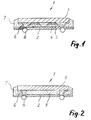
- a chip scale package 1 in two different ones Variants described.
- a preferably flexible carrier 2 made of plastic material, e.g. Polyimide film with a plurality of buffer cams 4 provided. These consist, for example, of a Silicone elastomer.
- a buffer cam 4 With help on this buffer cam an adhesive 5 attached to a silicon chip 3.
- On the free back of the carrier 2 are contact points in the shape of solder balls 8 arranged. These are about electrical Conductor 6 wired to the chip 3. All cavities between the buffer cams 4 and the area around the electrical conductors 6 are with a protective compound 7, for example filled out of plastic material.
- FIG. 2 differs the chip scale package 1 practically not from the outside that according to Figure 1. Instead of individual buffer cams however, a homogeneous adhesive layer 9 takes over Function of the buffer material and the spacer. After this Connect the electrical conductors 6 only in the Outside area are encapsulated with protective compound 7. The Danger of harmful influences from moisture thereby greatly reduced.
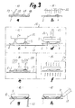
- Figure 3 shows the main workstations, their function is then explained.
- Figure 3a are at a Printing station using a stencil printing process individual Buffer cams printed on carrier 2.
- a template 18 is pressed against the carrier, which is provided with openings 21.
- a buffer mass 20 is pressed into the openings with a doctor blade 19, whereby the individual buffer cams are formed.
- the freshly formed buffer cams 4 are turned on according to Figure 3b a first hardening station 11 with a heat source 22.
- a carrier 2 prepared in this way now arrives on a Transport system 27 in a machine 26, in which side by side a dispensing station 12, a placement station 13 and optionally also a pre-hardening station 14 and / or a curing station 15 are arranged.
- a dispenser station 12 At the dispenser station 12 according to FIG. 3c is with a needle dispenser 23 an adhesive 5 from several tubes 24 simultaneously deposited each buffer cam 4. This will be an adhesive selected with the help of which gluing is carried out at room temperature can.
- the chip 3 is attached to the mounting station 13 according to FIG. 3d a placement head 25 on the coated buffer cams 4 discontinued. After a smooth, gentle onward transport a pre-hardening takes place to the pre-hardening station 14 according to FIG. 3e, preferably with the aid of infrared radiators 28, which irradiate the carrier 2 from above.
- Both stations that is Pre-hardening station and / or the hardening station could in certain cases may also be separate plant parts that are not can be run through with the same transport system.
- connection station 16 the electrical conductor 6 with a connecting tool 30 connected to the chip 3.
- This process (lead bonding) is already known per se to the person skilled in the art.
- the manufacturing process according to FIG. 4 works without the Formation of buffer cams.
- an adhesive 9 on the carrier 2 applied which also functions as a buffer mass takes over.
- the order is placed with the help of a movement dispenser 34, the one from a single needle 35 a certain Adhesive patterns, such as a cross or a star can draw on the carrier 2.
- the chip is placed on the adhesive 9 at the placement station 13 put on and with a small force against the carrier 2 pressed so that the previously drawn adhesive pattern under Displacement of the air forms a homogeneous layer.
- Pre-curing and / or curing in turn take place on the same way as in the previous embodiment.
- the wiring at station 16 is also the same.
- Figure 5 illustrates the arrangement of a group of settling positions on a carrier 2. Each position is with a plurality of buffer cams 4 provided. Such a thing The field of buffer cams is always with the needle dispenser according to FIG. 6 or in another way simultaneously with adhesive 5 coated.
- Figure 7 illustrates the size relationships, for example on the buffer cams. Accordingly, the diameter is a in the attachment area, for example, 450 ⁇ m and the maximum height b is 150 ⁇ m.
- the adhesive layer 5 has a maximum Diameter from about 350 to 450 microns, is therefore preferred slightly smaller than the area of the buffer cam.
- Figure 8 shows schematically an adjustment station 36, the immediate can be used at the touchdown station 13.
- the chip 3 becomes exact with the help of an adjustment optics 37 aligned with the underlying carrier 2 before or after he is discontinued.
- FIG. 9 schematically shows the rotary movement of a chip 3, between the removal of the wafer 38 and the placement on the Carrier.
- a pick-up arm 40 moves the chip from the wafer 38 a rotary holder 39.
- There the chip is turned and in next work cycle resumed from a delivery arm 41 and put down with the back against the carrier.
- FIG. 10 shows schematically how when the chip 3 is set down the mounting station of the carrier 2 by means of negative pressure on a Under pressure pad 42 can be fixed.
- the vacuum pad is provided with openings leading to a vacuum chamber to lead. There is a pressure below atmospheric lying pressure.
Abstract
Description
Die Erfindung betrifft ein Verfahren zum Verkapseln eines
elektronischen Bauteils, insbesondere eines Halbleiterchips,
gemäss dem Oberbegriff von Anspruch 1. Derartige Verfahren
erlauben die Herstellung sogenannter Chip-Scale-Packages
(CSP), bei denen das fertige mit Anschlussteilen versehene
Halbleiterelement nur unwesentlich grösser ist als der rohe
Siliciumchip.The invention relates to a method for encapsulating a
electronic component, in particular a semiconductor chip,
according to the preamble of
Die Grundidee besteht dabei darin, dass zwischen dem Träger und dem Bauteil eine Puffermasse, beispielsweise aus einem Silikon Elastomer angeordnet wird, welche die unterschiedlichen Längenausdehnungskoeffizienten der Werkstoffe kompensiert. Damit stehen auch die Lötverbindungen des eingebauten Halbleiterchips bei Erwärmung nur unter geringer Beanspruchung. Die Lebensdauer und Zuverlässigkeit derartiger Chip-Scale-Packages ist daher verhältnismässig hoch. Bekannte Herstellungsverfahren sind beispielsweise beschrieben in "Semiconductor International", November 1997, Seite 48, oder in US A-5-659-952 oder US-A-5-679-977. Trotz der verbesserten Eigenschaften des Endproduktes, sind die bekannten Verfahren aber noch relativ aufwendig und erlauben keine rationelle Fertigung. Es sind insbesondere zahlreiche Einzelschritte mit einem vergleichsweise hohen apparativen Aufwand erforderlich. Es ist daher eine Aufgabe der Erfindung, ein Verfahren der Eingangs genannten Art zu schaffen, bei dem weniger Prozessschritte erforderlich sind. Ausserdem soll beim Platzieren des Bauteils auf mechanische Anlageteile und/oder auf das Bauteil selbst keine unnötige Wärmeeinwirkung erfolgen, weil mikromechanische Prozesse unter gleichzeitiger Wärmeeinwirkung nur schwer zu handhaben sind. The basic idea is that between the carrier and the component a buffer mass, for example from a Silicone elastomer is arranged, which the different Coefficient of linear expansion of the materials compensated. This means that the solder connections of the built-in Semiconductor chips only slightly stressed when heated. The lifespan and reliability of such chip-scale packages is therefore relatively high. Known Manufacturing processes are described for example in "Semiconductor International", November 1997, page 48, or in US-A-5-659-952 or US-A-5-679-977. Despite the improved The properties of the end product are the known methods but still relatively complex and do not allow rational Production. There are in particular numerous individual steps with a comparatively high expenditure on equipment is required. It is therefore an object of the invention to provide a method of To create the type mentioned above, with fewer process steps required are. In addition, when placing of the component on mechanical system parts and / or on the Component itself does not cause unnecessary heat because micromechanical processes with simultaneous exposure to heat are difficult to handle.
Diese Aufgabe wird erfindungsgemäss mit einem Verfahren
gelöst, das die Merkmale im Anspruch 1 aufweist. Das Puffermaterial
und/oder ein Klebstoff wird dabei in flüssiger oder
pastöser Form aus einem Dispenser aufgetragen. Damit kann
zumindest ein bisher erforderlicher Arbeitsschritt eingespart
werden, nämlich das Aufdrucken eines Klebstoffes in einem
Schablonendruckverfahren. Das Bauteil selbst wird bei Raumtemperatur
auf das Puffermaterial und/oder auf den Klebstoff
aufgesetzt und nicht wie bisher im aufgeheizten Zustand.
Unter dem Begriff "Raumtemperatur" wird dabei eine Temperatur
verstanden, die in Arbeitsräumen entsprechnd der geltenden
Normen in der Klimatechnik herrscht und die etwa im Temperaturspektrum
von 10°C bis 45°C, vorzugsweise von 16°C bis 26°C
angesiedelt ist. Damit wird der Durchsatz pro Zeiteinheit
verbessert, weil keine Aufheizzeit für das Bauteil eingeplant
werden muss. Mechanische Anlagenteile und/oder Messinstrumente
werden nicht durch Wärmeeinwirkung beeinträchtigt.According to the invention, this object is achieved with a method
solved, which has the features in
Nach dem Aufsetzen des Bauteils kann das Puffermaterial und/oder der Klebstoff einer Vorhärtung und/oder einer Aushärtung unterzogen werden und zwar vorteilhaft auf der gleichen Anlage wie das Aufsetzen des Bauteils. Dadurch wird auf besonders vorteilhafte Weise der Umstand ausgenützt, dass bei den hier eingesetzten Klebstoffen das Zusammenfügen der zu verbindenden Teile und das Härten des Klebstoffes nicht zwingend zusammenfallen müssen. Durch die zeitliche Trennung kann das Vorhärten und/oder das Aushärten in einem Anlagenbereich erfolgen, bei dem Wärmeentwicklung weniger problematisch ist. Nach dem Vorhärten oder Aushärten können die verbundenen Einheiten ohne Risiko einer gegenseitigen Verschiebung von Träger und Bauteil zu beliebigen anderen Arbeitsstationen transportiert werden.After placing the component, the buffer material can and / or the adhesive of a pre-hardening and / or a hardening be subjected to and advantageously on the same System like the placement of the component. This will turn on particularly advantageous way of taking advantage of the fact that the adhesives used here to join the connecting parts and the hardening of the adhesive must coincide. Because of the time separation can pre-harden and / or harden in a plant area take place where heat development is less problematic is. After pre-curing or curing, the connected units without risk of mutual displacement from carrier and component to any other workstations be transported.
Eine wesentliche Prozessvereinfachung kann erreicht werden, indem zuerst mehrere Puffernocken in einem Schablonendruckverfahren befestigt werden, die Puffernocken ausgehärtet werden und vor dem Aufsetzen des Bauteils mit dem Dispenser auf und/oder neben mehreren Puffernocken Klebstoff aufgetragen wird. Bei diesem Verfahren können bestehende Schablonendrucker für das Auftragen der Puffernocken (Nubbins) verwendet werden. Dagegen erfolgt der Auftrag des Klebstoffs auf erheblich einfachere Weise mit dem Dispenser. Vorteilhaft wird gleichzeitig aus mehreren Dispenseröffnungen Klebestoff aufgetragen. Denkbar wäre unter Umständen aber auch ein Dispenser, der in rascher Folge hintereinander eine Gruppe von Puffernocken mit einem Klebstoff beschichtet.A significant process simplification can be achieved by first printing several buffer cams in a stencil printing process attached, the buffer cams hardened and before placing the component with the dispenser applied to and / or next to several buffer cams adhesive becomes. Existing stencil printers can use this method used for the application of the buffer cams (nubbins) become. In contrast, the adhesive is applied much easier way with the dispenser. Advantageous becomes adhesive from several dispenser openings at the same time applied. Under certain circumstances, a dispenser would also be conceivable who in quick succession a group of Buffer cams coated with an adhesive.
Bei geeigneter Materialwahl können mit dem Dispenser aber auch die Puffernocken selbst auf den Träger abgesetzt und befestigt werden. Anschliessend kann jeder Puffernocken mit einer Kelbstoffschicht versehen werden. Dies kann entweder mit einem separaten Dispenser oder mit dem gleichen Dispenser erfolgen.With a suitable choice of material you can use the dispenser also set the buffer cams themselves on the carrier and be attached. Then each buffer cam can be used be provided with a layer of woven fabric. This can either with a separate dispenser or with the same dispenser respectively.
Eine weitere wesentliche Vereinfachung des Prozesses kann schliesslich dadurch erreicht werden, dass mit dem Dispenser auf den Träger ein Klebstoff aufgetragen wird, der gleichzeitig als Puffermaterial dient. Damit entfällt die Aufteilung in zwei separate Werkstoffe, was den Prozess insgesamt vereinfacht. Der Klebstoff kann dabei in der Form einzelner Pufferkörper aufgetragen werden, welche nach dem Aufsetzen des Bauteils vereinzelt bleiben. Die Zwischenräume werden dabei später zusammen mit der Umhüllung der Verdrahtungsstellen mit einer Schutzmasse ausgefüllt. Alternativ ist es aber auch denkbar, dass der Klebstoff mit dem Dispenser als Klebstoffmuster aufgetragen wird, das sich nach dem Aufsetzen des Bauteils zu einer homogenen Schicht verbindet. Dadurch werden Lufteinschlüsse verhindert und ein nachträgliches Ausfüllen der Zwischenräume ist nicht mehr nötig. Derartige Klebstoffmuster sind in der Halbleiter-Verkaspelungstechnik bereits bekannt. Another significant simplification of the process can can finally be achieved by using the dispenser an adhesive is applied to the carrier at the same time serves as a buffer material. This eliminates the division in two separate materials, which simplifies the process overall. The adhesive can be in the form of individual Buffer bodies are applied, which after placing of the component remain isolated. The spaces in between later together with the covering of the wiring points filled with a protective compound. Alternatively it is but also conceivable that the adhesive with the dispenser as Adhesive pattern is applied, which is after touchdown of the component to form a homogeneous layer. Thereby air pockets are prevented and a subsequent It is no longer necessary to fill in the gaps. Such Adhesive patterns are used in semiconductor encapsulation technology already known.
Weitere Vorteile können erreicht werden, wenn das Auftragen des Puffermaterials und/oder des Klebstoffs mit dem Dispenser unmittelbar vor dem Aufsetzen des Bauteils auf der gleichen Maschine erfolgt. Vorteilhaft wird dabei auch der Träger auf dem gleichen Transportsystem am Dispenser und an der Aufsetzvorrichtung für das Bauteil vorbeigeführt. Einerseits können dabei die beiden Arbeitsschritte exakt aufeinander abgestimmt werden und die Trockenzeit kann besser kontrolliert werden. In der gleichen Maschine und auf dem gleichen Transportsystem ist ein ruckfreier und sanfter Transport möglich, wodurch die Gefahr einer unbeabsichtigten Verschiebung des Bauteils aus der Soll-Lage stark reduziert wird. Vor dem Aufsetzen wird das Bauteil vorteilhaft lagemässig justiert.Additional benefits can be achieved when applying the buffer material and / or the adhesive with the dispenser immediately before placing the component on the same Machine is done. The carrier is also advantageous the same transport system on the dispenser and on the attachment device passed for the component. On the one hand can the two work steps are precisely coordinated and the drying time can be better controlled. In the same machine and on the same transport system a smooth and smooth transport is possible, which makes the Danger of inadvertent displacement of the component the target position is greatly reduced. Before putting on the component is advantageously adjusted in position.
Eine Verbesserung der Planarität von Bauteil und Träger kann dadurch erreicht werden, dass der Träger wenigstens beim Aufsetzen des Bauteils mittels Unterdruck auf einer Auflagefläche fixiert wird.The planarity of component and carrier can be improved can be achieved in that the carrier at least at Placing the component on a support surface using negative pressure is fixed.
Zur Verbesserung der Fertigungsrationalität werden vorteilhaft auf dem gleichen Träger Gruppen von Bauteilen befestigt. Dazu werden jeweils mehrere Bauteile nacheinander zu einer Gruppe abgesetzt. Die ganze Gruppe kann dann gleichzeitig einem Anpressdruck und/oder einer Wärmebehandlung ausgesetzt werden. Dieses gruppenweise Anpressen und/oder Heizen kann auch bei alternativen Verkapselungsprozessen eingesetzt werden, bei denen das Bauteil nicht bei Raumtemperatur abgesetzt wird. Die gleichzeitige Bearbeitung der Bauteile kann über gemeinsam betätigte Einzelwerkzeuge erfolgen, wie z.B. einzelne Anpressstempel, welche aber gleichzeitig betätigt werden. Alternativ kann es sich aber auch um ein gemeinsames Werkzeug handeln, das die ganze Gruppe gleichzeitig beaufschlagt, wie z.B. ein gemeinsamer Pressstempel von entsprechender Grösse.To improve manufacturing rationality will be beneficial groups of components attached to the same support. For this purpose, several components are made into one after the other Group discontinued. The whole group can then do it at the same time exposed to a contact pressure and / or a heat treatment become. This pressing and / or heating in groups can also used in alternative encapsulation processes where the component is not deposited at room temperature becomes. The simultaneous processing of the components can via jointly operated individual tools, e.g. individual contact stamps, which are actuated at the same time become. Alternatively, it can also be a common one Act tools that affect the whole group at the same time, such as. a common press stamp of the appropriate type Size.
Die Erfindung betrifft auch eine Vorrichtung zur Durchführung
des beschriebenen Verfahrens, welche durch die Merkmale im
Anspruch 15 gekennzeichnet ist. Mit geringfügigen baulichen
Adaptionen können dabei vorteilhaft bekannte Bestückungsautomaten
(Die bonder) eingesetzt werden, wie sie z.B. durch
die WO 97/32460 bekannt geworden sind.The invention also relates to a device for carrying it out
of the described method, which is characterized by the features in
Die Dispenserstation kann einen Dispenser mit mehreren Ausgabeöffnungen oder aber einen Dispenser mit wenigstens einer beweglichen Dispenseröffnung aufweisen, mit dessen Hilfe durch gleichzeitige Bewegung und Abgabe des Mittels ein bestimmtes Muster gezeichnet werden kann.The dispenser station can be a dispenser with several dispensing openings or a dispenser with at least one Have movable dispenser opening, with the help by simultaneously moving and dispensing the agent certain pattern can be drawn.
Eine besonders kompakte Fertigungseinheit kann erzielt werden, wenn in Transportrichtung nach der Aufsetzstation eine Vorhärtestation und/oder eine Aushärtestation angeordnet ist, in welcher die aus Träger und Bauteil bestehende Einheit mittels elektromagnetischer Strahlen, insbesondere mittels Infrarotstrahlen oder Ultraviolettstrahlen beaufschlagbar ist. Die Halbleiterbauteile können diese Vorhärtestation oder Aushärtestation im gleichen Arbeitstakt durchlaufen wie die Dispenserstation und die Aufsetzstation.A particularly compact manufacturing unit can be achieved if in the direction of transport after the mounting station Pre-curing station and / or a curing station is arranged, in which the unit consisting of carrier and component by means of electromagnetic radiation, in particular by means of Infrared rays or ultraviolet rays can be applied is. The semiconductor components can this pre-hardening station or Curing station in the same work cycle as the Dispenser station and the placement station.
Weitere Vorteile und Einzelmerkmale der Erfindung ergeben sich aus der nachfolgenden Beschreibung und aus den Zeichnungen. Es zeigen
Figur 1- einen Querschnitt durch ein Chip-Scale-Package mit einzelnen Puffernocken,
Figur 2- einen Querschnitt durch ein Chip-Scale-Package mit einer homogenen Pufferschicht,
Figur 3- ein erstes Herstellungsverfahren in schematischen Einzeldarstellungen,
Figur 4- ein zweites Herstellungsverfahren in schematischen Einzeldarstellungen,
Figur 5- eine Draufsicht auf einen Träger mit einer Gruppe von Absetzpositionen für Bauteile,
Figur 6- eine schematische Darstellung eines Nadeldispensers mit mehreren Abgabeöffnungen,
Figur 7- stark vergrösserte Puffernocken mit Klebstoffschicht in Seitenansicht,
Figur 8- die schematische Darstellung einer Justierstation,
Figur 9- die schematische Darstellung einer Aufsetzstation, und
Figur 10- eine schematische Darstellung eines Aufsetzvorgangs.
- Figure 1
- a cross section through a chip scale package with individual buffer cams,
- Figure 2
- 3 shows a cross section through a chip scale package with a homogeneous buffer layer,
- Figure 3
- a first manufacturing process in schematic individual representations,
- Figure 4
- a second manufacturing process in schematic individual representations,
- Figure 5
- 3 shows a plan view of a carrier with a group of depositing positions for components,
- Figure 6
- 1 shows a schematic representation of a needle dispenser with several dispensing openings,
- Figure 7
- greatly enlarged buffer cams with adhesive layer in side view,
- Figure 8
- the schematic representation of an adjustment station,
- Figure 9
- the schematic representation of a landing station, and
- Figure 10
- a schematic representation of a placement process.
Anhand der Figuren 1 und 2 wird zunächst der prinzipielle
Aufbau eines Chip-Scale-Package 1 in zwei unterschiedlichen
Varianten beschrieben. Beim Ausführungsbeispiel gemäss Figur
1 ist ein vorzugsweise flexibler Träger 2 aus Kunststoffmaterial,
z.B. Polyimidfolie mit einer Mehrzahl von Puffernocken
4 versehen. Diese bestehen beispielsweise aus einem
Silikon Elastomer. Auf diesen Puffernocken ist mit Hilfe
eines Klebstoffs 5 ein Siliciumchip 3 befestigt. Auf der
freibleibenden Rückseite des Trägers 2 sind Kontaktstellen in
der Form von Lötkugeln 8 angeordnet. Diese sind über elektrische
Leiter 6 mit dem Chip 3 verdrahtet. Sämtliche Hohlräume
zwischen den Puffernocken 4 sowie der Bereich um die
elektrischen Leiter 6 sind mit einer Schutzmasse 7 beispielsweise
aus Kunststoffmaterial ausgefüllt. Das Anbringen und
Verbinden der elektrischen Leiter, das Befestigen der Lötkugeln
und auch das Ausfüllen der Zwischenräume ist dem Fachmann
an sich bereits bekannt und wird im Folgenden nicht mehr
näher beschrieben. Es wird in diesem Zusammenhang hingewiesen
auf Lawing, "Preventing voids in µBGA® packages", in Chip
Scale Review März 1998. Brauchbare Silikon Elastomere werden
beispielsweise von der Firma Dow Corning, Midland, Michigan
USA hergestellt, nämlich unter der Bezeichnung Dow Corning
7910 für den Klebstoff, Dow Corning 6910 für das Puffermaterial
und Dow Corning 6811 für die Schutzmasse.With the aid of FIGS. 1 and 2, the principle is first
Structure of a
Beim Ausführungsbeispiel gemäss Figur 2 unterscheidet sich
das Chip-Scale-Package 1 von aussen praktisch nicht von
demjenigen gemäss Figur 1. Anstelle von einzelnen Puffernocken
übernimmt jedoch eine homogene Klebstoffschicht 9 die
Funktion des Puffermaterials und des Abstandhalters. Nach dem
Verbinden der elektrischen Leiter 6 müssen diese nur noch im
Aussenbereich mit der Schutzmasse 7 verkapselt werden. Die
Gefahr von schädlichen Einflüssen von Feuchtigkeit wird
dadurch stark reduziert.The embodiment in FIG. 2 differs
the
Das in Figur 3 schematisch dargestellte Herstellungsverfahren
zeigt die wesentlichen Arbeitsstationen, deren Funktion
anschliessend erläutert wird. In Figur 3a werden an einer
Druckstation mit Hilfe eines Schablonendruckverfahrens einzelne
Puffernocken auf den Träger 2 aufgedruckt. Zu diesem
Zweck wird eine Schablone 18 gegen den Träger gepresst,
welche mit Öffnungen 21 versehen ist. Eine Puffermasse 20
wird mit einem Rakel 19 in die Öffnungen gepresst, wodurch
die einzelnen Puffernocken gebildet werden.The manufacturing process shown schematically in Figure 3
shows the main workstations, their function
is then explained. In Figure 3a are at a
Printing station using a stencil printing process individual
Buffer cams printed on
Die frisch geformten Puffernocken 4 werden gemäss Figur 3b an
einer ersten Härtestation 11 mit einer Wärmequelle 22 ausgehärtet.The freshly formed
Ein derart vorbereiteter Träger 2 gelangt jetzt auf einem
Transportsystem 27 in eine Maschine 26, in welcher nebeneinander
eine Dispenserstation 12, eine Aufsetzstation 13 und
gegebenenfalls auch noch eine Vorhärtestation 14 und/oder
eine Aushärtestation 15 angeordnet sind. An der Dispenserstation
12 gemäss Figur 3c wird mit einem Nadeldispenser 23
aus mehreren Röhrchen 24 gleichzeitig ein Klebstoff 5 auf
jedem Puffernocken 4 abgesetzt. Dabei wird ein Klebstoff
gewählt, mit dessen Hilfe bei Raumtemperatur geklebt werden
kann.A
An der Aufsetzstation 13 gemäss Figur 3d wird der Chip 3 mit
einem Aufsetzkopf 25 auf die beschichteten Puffernocken 4
abgesetzt. Nach einem ruckfreien schonenden Weitertransport
zur Vorhärtestation 14 gemäss Figur 3e erfolgt eine Vorhärtung,
vorzugsweise mit Hilfe von Infrarotstrahlern 28, welche
den Träger 2 von oben bestrahlen.The
Erst nach dieser Vorhärtung wird gemäss Figur 3f die ganze
Einheit an einer Härtestation 15 mit einem Ofen 29 mit einer
Temperatur von beispielsweise 150°C ausgehärtet.Only after this pre-hardening is the whole according to FIG. 3f
Unit at a hardening
Anstelle der Vorhärtestation könnte aber auch unmittelbar die endgültige Aushärtestation treten. Beide Stationen, also die Vorhärtestation und/oder die Aushärtestation könnten in bestimmten Fällen auch separate Anlagenteile sein, die nicht mit dem gleichen Transportsystem durchlaufen werden können.Instead of the pre-hardening station, the final curing station. Both stations, that is Pre-hardening station and / or the hardening station could in certain cases may also be separate plant parts that are not can be run through with the same transport system.
Anschliessend werden gemäss Figur 3g an einer Verbindungsstation
16 die elektrischen Leiter 6 mit einem Verbindungswerkzeug
30 an den Chip 3 angeschlossen. Dieser Prozess (Lead
bonding) ist dem Fachmann an sich bereits bekannt.Then according to Figure 3g at a
Schliesslich erfolgt gemäss Figur 3h das Verkapseln der
ganzen Einheit mit einer Schutzmasse 7 die aus einem Füllwerkzeug
31 abgegeben wird. Dabei werden die Hohlräume zwischen
den einzelnen Puffernocken 4 und auch die Verdrahtungen
ausgefüllt bzw. umhüllt. Finally, according to FIG. 3h, the encapsulation of the
whole unit with a
Das Herstellungsverfahren gemäss Figur 4 arbeitet ohne die
Bildung von Puffernocken. Dagegen wird an der Dispenserstation
12 gemäss Figur 5a ein Klebstoff 9 auf den Träger 2
aufgetragen, der gleichzeitig die Funktion einer Puffermasse
übernimmt. Der Auftrag erfolgt mit Hilfe eines Bewegungsdispensers
34, der aus einer Einfachnadel 35 ein bestimmtes
Klebstoffmuster, beispielsweise ein Kreuz oder einen Stern
auf den Träger 2 zeichnen kann.The manufacturing process according to FIG. 4 works without the
Formation of buffer cams. In contrast, at the
Anstelle eines linienförmigen Musters könnten auch einzelne Flächen aufgetragen werden. Anstelle einer Einfachnadel könnte auch ein Werkzeug mit Mehrfachöffnungen eingesetzt werden.Instead of a linear pattern, individual ones could also be used Surfaces are applied. Instead of a single needle a tool with multiple openings could also be used become.
An der Aufsetzstation 13 wird der Chip auf den Klebstoff 9
aufgesetzt und mit einer geringen Kraft gegen den Träger 2
gepresst, sodass das vorher gezeichnete Klebstoffmuster unter
Verdrängung der Luft eine homogene Schicht bildet.The chip is placed on the adhesive 9 at the
Vorhärtung und/oder Aushärtung erfolgen wiederum auf die
gleiche Weise wie beim vorhergehenden Ausführungsbeispiel.
Auch die Verdrahtung an der Station 16 ist gleich.Pre-curing and / or curing in turn take place on the
same way as in the previous embodiment.
The wiring at
An der Verkapselungsstation 17 wird zwar ebenfalls eine
Schutzmasse 7 ausgestossen. Diese muss aber nur noch die
elektrischen Leiter 6 und die Seitenkanten des Chips 3 umhüllen.
Falls die Pufferschicht nicht homogen ist, sondern in
einzelne Abschnitte unterteilt ist, müssen allerdings an der
Verkapselungsstation 17 auch diese Hohlräume ausgefüllt
werden. Schliesslich sei auch noch darauf hingewiesen, dass
die Verdrahrungsstelle nicht zwingend im äusseren Bereich der
Bauteile 3 angeordnet sein müssen. Auch eine Verdrahtung
innerhalb der Fläche der Bauteile ist in der Paxis möglich.At the
Figur 5 veranschaulicht die Anordnung einer Gruppe von Absetzpositionen
auf einem Träger 2. Jede Position ist mit
einer Mehrzahl von Puffernocken 4 versehen. Ein derartiges
Feld von Puffernocken wird jeweils mit dem Nadeldispenser
gemäss Figur 6 oder auf andere Weise gleichzeitig mit Klebstoff
5 beschichtet.Figure 5 illustrates the arrangement of a group of settling positions
on a
Figur 7 veranschaulicht die Grössenverhältnisse beispielsweise
an den Puffernocken. Demnach beträgt der Durchmesser a
im Ansatzbereich beispielsweise 450 µm und die maximale Höhe
b liegt bei 150 µm. Die Klebstoffschicht 5 hat einen maximalen
Durchmesser von ca. 350 bis 450 µm, ist also vorzugsweise
etwas kleiner als die Fläche des Puffernockens.Figure 7 illustrates the size relationships, for example
on the buffer cams. Accordingly, the diameter is a
in the attachment area, for example, 450 µm and the maximum height
b is 150 µm. The
Figur 8 zeigt schematisch eine Justierstation 36, die unmittelbar
an der Aufsetzstation 13 eingesetzt werden kann.
Dabei wird mit Hilfe einer Justieroptik 37 der Chip 3 exakt
auf den darunterliegenden Träger 2 ausgerichtet, bevor oder
nachdem er abgesetzt wird.Figure 8 shows schematically an
Figur 9 zeigt schematisch die Drehbewegung eines Chips 3,
zwischen der Wegnahme vom Wafer 38 und dem Aufsetzen auf den
Träger. Ein Aufnahmearm 40 bewegt den Chip vom Wafer 38 zu
einen Drehhalter 39. Dort wird der Chip gewendet und im
nächsten Arbeitstakt von einem Abgabearm 41 wieder aufgenommen
und mit der Rückseite gegen den Träger wieder abgelegt.FIG. 9 schematically shows the rotary movement of a
Figur 10 zeigt schematisch, wie beim Absetzen des Chips 3 an
der Aufsetzstation der Träger 2 mittels Unterdruck auf einer
Unterdurckauflage 42 fixiert werden kann. Die Unterdruckauflage
ist mit Öffnungen versehen, welche zu einer Unterdruckkammer
führen. Dort herrscht ein unter dem Atmosphärendruck
liegender Druck.FIG. 10 shows schematically how when the
Claims (20)
Priority Applications (12)
| Application Number | Priority Date | Filing Date | Title |
|---|---|---|---|
| EP99810009A EP1018760A1 (en) | 1999-01-07 | 1999-01-07 | Method and apparatus for encapsulating an electronic device, especially a semiconductor chip |
| AT99112660T ATE270790T1 (en) | 1999-01-07 | 1999-07-02 | METHOD AND DEVICE FOR TREATING ELECTRONIC COMPONENTS ARRANGE ON A SUBSTRATE, IN PARTICULAR SEMICONDUCTOR CHIPS |
| EP99112660.8A EP1030349B2 (en) | 1999-01-07 | 1999-07-02 | Method and apparatus for treating electronic components mounted on a substrate, in particular semiconductor chips |
| DE59909906T DE59909906D1 (en) | 1999-01-07 | 1999-07-02 | Method and device for treating electronic components arranged on a substrate, in particular of semiconductor chips |
| ES99112660T ES2224501T3 (en) | 1999-01-07 | 1999-07-02 | PROCEDURE AND DEVICE FOR THE TREATMENT OF COMPONENTS PROPOSED ON A SUBSTRATE, ESPECIALLY OF SEMI-CONDUCTOR CHIPS. |
| PT99112660T PT1030349E (en) | 1999-01-07 | 1999-07-02 | A PROCESS AND DEVICE FOR THE MANIPULATION OF CONSTRUCTION PASTES PLACED ON A SUBSTRATE PARTICULARLY SEMICONDUCTOR CHIPS |
| MYPI99005529A MY130850A (en) | 1999-01-07 | 1999-12-17 | Method and apparatus for treating electronic components mounted on a substrate, in particular semiconductor chips |
| PCT/CH1999/000621 WO2000041219A1 (en) | 1999-01-07 | 1999-12-22 | Method and device for processing components, notably semiconductor chips, arranged on a substrate |
| JP2000592863A JP2002534799A (en) | 1999-01-07 | 1999-12-22 | Method and apparatus for processing components arranged on a substrate, especially semiconductor chips |
| PCT/CH1999/000620 WO2000041234A1 (en) | 1999-01-07 | 1999-12-22 | Method and device for encapsulating an electronic component, notably a semiconductor chip |
| KR1020017008579A KR20010108071A (en) | 1999-01-07 | 1999-12-22 | Method and device for processing components, notably semiconductor chips, arranged on a substrate |
| US09/478,411 US6621157B1 (en) | 1999-01-07 | 2000-01-06 | Method and device for encapsulating an electronic component in particular a semiconductor chip |
Applications Claiming Priority (1)
| Application Number | Priority Date | Filing Date | Title |
|---|---|---|---|
| EP99810009A EP1018760A1 (en) | 1999-01-07 | 1999-01-07 | Method and apparatus for encapsulating an electronic device, especially a semiconductor chip |
Publications (1)
| Publication Number | Publication Date |
|---|---|
| EP1018760A1 true EP1018760A1 (en) | 2000-07-12 |
Family
ID=8242628
Family Applications (1)
| Application Number | Title | Priority Date | Filing Date |
|---|---|---|---|
| EP99810009A Withdrawn EP1018760A1 (en) | 1999-01-07 | 1999-01-07 | Method and apparatus for encapsulating an electronic device, especially a semiconductor chip |
Country Status (6)
| Country | Link |
|---|---|
| EP (1) | EP1018760A1 (en) |
| AT (1) | ATE270790T1 (en) |
| DE (1) | DE59909906D1 (en) |
| ES (1) | ES2224501T3 (en) |
| PT (1) | PT1030349E (en) |
| WO (1) | WO2000041234A1 (en) |
Cited By (1)
| Publication number | Priority date | Publication date | Assignee | Title |
|---|---|---|---|---|
| CN110740575A (en) * | 2019-09-11 | 2020-01-31 | 黄诚 | production and processing equipment for integrated circuit board |
Families Citing this family (1)
| Publication number | Priority date | Publication date | Assignee | Title |
|---|---|---|---|---|
| DE10250778B3 (en) * | 2002-10-30 | 2004-03-04 | Infineon Technologies Ag | Semiconductor chip used in flip-chip technology for producing circuit boards has a buffer body with a protective layer made from a damping material arranged between a contact surfaces and above a semiconductor component structures |
Citations (4)
| Publication number | Priority date | Publication date | Assignee | Title |
|---|---|---|---|---|
| US5659952A (en) * | 1994-09-20 | 1997-08-26 | Tessera, Inc. | Method of fabricating compliant interface for semiconductor chip |
| WO1997033312A1 (en) * | 1996-03-07 | 1997-09-12 | Tessera, Inc. | Method of encapsulating a semiconductor package |
| EP0886313A1 (en) * | 1996-12-04 | 1998-12-23 | Shinko Electric Industries Co. Ltd. | Semiconductor device sealed with resin, and its manufacture |
| EP0898305A2 (en) * | 1997-08-20 | 1999-02-24 | Oki Electric Industry Co., Ltd. | Structure and method for packaging semiconductor chip |
-
1999
- 1999-01-07 EP EP99810009A patent/EP1018760A1/en not_active Withdrawn
- 1999-07-02 DE DE59909906T patent/DE59909906D1/en not_active Expired - Lifetime
- 1999-07-02 AT AT99112660T patent/ATE270790T1/en active
- 1999-07-02 PT PT99112660T patent/PT1030349E/en unknown
- 1999-07-02 ES ES99112660T patent/ES2224501T3/en not_active Expired - Lifetime
- 1999-12-22 WO PCT/CH1999/000620 patent/WO2000041234A1/en active Search and Examination
Patent Citations (4)
| Publication number | Priority date | Publication date | Assignee | Title |
|---|---|---|---|---|
| US5659952A (en) * | 1994-09-20 | 1997-08-26 | Tessera, Inc. | Method of fabricating compliant interface for semiconductor chip |
| WO1997033312A1 (en) * | 1996-03-07 | 1997-09-12 | Tessera, Inc. | Method of encapsulating a semiconductor package |
| EP0886313A1 (en) * | 1996-12-04 | 1998-12-23 | Shinko Electric Industries Co. Ltd. | Semiconductor device sealed with resin, and its manufacture |
| EP0898305A2 (en) * | 1997-08-20 | 1999-02-24 | Oki Electric Industry Co., Ltd. | Structure and method for packaging semiconductor chip |
Non-Patent Citations (1)
| Title |
|---|
| MITCHELL C: "Advancements in CSP encapsulation: Process and material", PAN PACIFIC MICROELECTRONICS SYMPOSIUM. PROCEEDINGS OF THE TECHNICAL PROGRAM, PROCEEDINGS OF PAN PACIFIC MICROELECTRONICS SYMPOSIUM, KONA, HI, USA, 10-13 FEB. 1998, 1998, EDINA, MN, USA, SURFACE MOUNT TECHNOL. ASSOC, USA, PAGE(S) 137 - 140, XP002107244 * |
Cited By (1)
| Publication number | Priority date | Publication date | Assignee | Title |
|---|---|---|---|---|
| CN110740575A (en) * | 2019-09-11 | 2020-01-31 | 黄诚 | production and processing equipment for integrated circuit board |
Also Published As
| Publication number | Publication date |
|---|---|
| WO2000041234A1 (en) | 2000-07-13 |
| DE59909906D1 (en) | 2004-08-12 |
| ES2224501T3 (en) | 2005-03-01 |
| ATE270790T1 (en) | 2004-07-15 |
| PT1030349E (en) | 2004-11-30 |
Similar Documents
| Publication | Publication Date | Title |
|---|---|---|
| EP1030349B1 (en) | Method and apparatus for treating electronic components mounted on a substrate, in particular semiconductor chips | |
| DE10334576B4 (en) | Method for producing a semiconductor component with a plastic housing | |
| DE19720275B4 (en) | Substrate for a semiconductor device, manufacturing method for the same and a stackable semiconductor device using the substrate | |
| EP1796137B1 (en) | Apparatus and clocked method for pressure sintering | |
| DE3805572C2 (en) | Carrier tape for electronic components and method for producing a sequence of electronic components | |
| DE10102197A1 (en) | Multiple chip component with wireless packing has dies or chip elements with bumps on lower line frames, upper line frames coupled to dies, connecting rails interconnected in pairs | |
| DE19628237A1 (en) | Semiconductor device and manufacturing method of the same | |
| DE19723202A1 (en) | Crack resistant semiconductor component production | |
| DE102008033651B4 (en) | Method for producing a power semiconductor module | |
| EP2852970A1 (en) | Method for producing an electronic subassembly | |
| DE60207282T2 (en) | CAPTURE THE CONNECTION LOT TO MAINTAIN THE ACCURACY OF THE CONNECTION POSITION | |
| WO2001063605A1 (en) | Method and device for producing a dvd | |
| EP0002496A1 (en) | Method and apparatus for aligning flat and thin workpieces | |
| EP1204137A2 (en) | Semiconductor Chip Contacting Method and Apparatus | |
| EP1398828A2 (en) | Semiconductor package with a precured polymer encapsulating compound and method for manufacturing the same | |
| DE102005015036B4 (en) | Method for mounting a chip on a substrate | |
| DE2108850C2 (en) | Method for attaching leads to semiconductor wafers | |
| EP1018760A1 (en) | Method and apparatus for encapsulating an electronic device, especially a semiconductor chip | |
| DE102005006978B3 (en) | Method for joining semiconductor components with a flexible support band comprises moving an endless band parallel to the running direction of the support band between heating elements and the components | |
| WO1996002955A1 (en) | Process for producing an electrically conductive connection | |
| DE19819054B4 (en) | Method and device for mounting and adjusting components on a mounting base | |
| EP0644507B1 (en) | Manufacturing method and device for a chip-card module | |
| DE10327515B4 (en) | Method for producing a substrate-based IC package | |
| DE102021121625B3 (en) | Method for producing an electronic assembly having at least one active electronic component and at least one passive component | |
| DE10394148T5 (en) | Improved method and apparatus for positioning integrated circuits on die pads |
Legal Events
| Date | Code | Title | Description |
|---|---|---|---|
| PUAI | Public reference made under article 153(3) epc to a published international application that has entered the european phase |
Free format text: ORIGINAL CODE: 0009012 |
|
| AK | Designated contracting states |
Kind code of ref document: A1 Designated state(s): AT CH DE FI FR GB IT LI NL PT SE |
|
| AX | Request for extension of the european patent |
Free format text: AL;LT;LV;MK;RO;SI |
|
| 17P | Request for examination filed |
Effective date: 20001009 |
|
| AKX | Designation fees paid |
Free format text: AT CH DE FI FR GB IT LI NL PT SE |
|
| AXX | Extension fees paid |
Free format text: LT PAYMENT 20001009;LV PAYMENT 20001009 |
|
| STAA | Information on the status of an ep patent application or granted ep patent |
Free format text: STATUS: THE APPLICATION IS DEEMED TO BE WITHDRAWN |
|
| 18D | Application deemed to be withdrawn |
Effective date: 20020801 |