EP1018834A2 - Electrophotographic apparatus and method - Google Patents
Electrophotographic apparatus and method Download PDFInfo
- Publication number
- EP1018834A2 EP1018834A2 EP99305299A EP99305299A EP1018834A2 EP 1018834 A2 EP1018834 A2 EP 1018834A2 EP 99305299 A EP99305299 A EP 99305299A EP 99305299 A EP99305299 A EP 99305299A EP 1018834 A2 EP1018834 A2 EP 1018834A2
- Authority
- EP
- European Patent Office
- Prior art keywords
- optical energy
- dot
- dots
- control unit
- light control
- Prior art date
- Legal status (The legal status is an assumption and is not a legal conclusion. Google has not performed a legal analysis and makes no representation as to the accuracy of the status listed.)
- Granted
Links
Images


Classifications
-
- H—ELECTRICITY
- H04—ELECTRIC COMMUNICATION TECHNIQUE
- H04N—PICTORIAL COMMUNICATION, e.g. TELEVISION
- H04N1/00—Scanning, transmission or reproduction of documents or the like, e.g. facsimile transmission; Details thereof
- H04N1/40—Picture signal circuits
- H04N1/40025—Circuits exciting or modulating particular heads for reproducing continuous tone value scales
- H04N1/40037—Circuits exciting or modulating particular heads for reproducing continuous tone value scales the reproducing element being a laser
Definitions
- the present invention relates generally to an electrophotographic apparatus and method for use in a printer, a facsimile, etc., in which dot latent images in conformity with binarized image dot data are formed on a photosensitive drum through scanning of an LED array or a laser beam and in which after development of the latent images with toners the resultant dots are transferred onto record paper, and more particularly to an electrophotographic apparatus and method providing control of appropriate quantity of light emission taking into consideration the influence of light from illuminating peripheral dots.
- record paper is conveyed at a certain speed by a paper conveyance mechanism so that images are recorded on the record paper through the electrophotographic process executed by electrostatic recording units arranged in the record paper conveyance direction.
- the electrostatic recording unit forms latent images in conformity with image dot data by means of LED array line scanning or laser diode laser beam scanning on a photosensitive drum in rotation, and after development with toner components, transfers the developed images onto record paper.
- color electrophotographic apparatuses for recording color images have also been put into practice.
- the color electrophotographic apparatus comprises four electrostatic recording units of black (K), cyan (C), magenta (M) and yellow (Y) in a tandem manner in the record paper conveyance direction.
- the electrostatic recording units for four colors optically scan the photosensitive drums on the basis of image data to form latent images, develop the latent images with color toners in developing vessels, transfer the developed images onto record paper being conveyed at a certain speed in a superposed manner in the order of yellow (Y), magenta (M), cyan (C) and black (K), and finally perform thermal fixing through a fixing device or other processes.
- Fig. 1 shows a relationship between a latent image and a bias voltage in the case where the photosensitive drum has been subjected to optical energy capable of developing the single isolated dot in the electrophotographic process.
- a latent image 200 is not developed as a toner image at a specific bias voltage Vth or below, but it is developed as a toner image 202 at a voltage exceeding the bias voltage Vth, with the dot size of W1.
- the optical energy equal to Fig.
- the drawbacks that the emission of light of a plurality of adjoining dots may cause too large a dot size and that no isolated dot may be formed by the high-density optical energy, will be attributable to the non-linear relationship as shown in Fig. 5, in which the relation between the developed dot diameter and the optical energy is not linear. That is, the dots are not formed with an optical energy L short of a certain threshold value Lth. Once the optical energy exceeds the threshold value Lth, the dot diameter W sharply increases in accordance with the increase of the optical energy P. Afterwards, increase of the dot diameter W gradually reaches a limit along with the increase of the optical energy P.
- an electrophotographic apparatus and method capable of faithfully developing and recording dots irrespective of dot patterns, by appropriately controlling optical energy for light-emission taking into consideration the fact that optical energies mutually influence each other between adjacent dots.
- the electrophotographic apparatus of the present invention comprises an electrostatic recording unit and a quantity-of-light control unit.
- the electrostatic recording unit forms a dot latent image in conformity with binarized image dot data by directing a scanning light beam onto a latent image carrier in motion, e.g., a rotating photosensitive drum arranged in the record paper conveyance direction, and after development with a toner component, transfers dots onto record paper for development.
- the quantity-of-light control unit controls, for each emitted noticeable dot (visible or discernible dot) in the image data, the optical energy for use in formation of a latent image of the noticeable dot, on the basis of peripheral dots which may have influence on the size of the noticeable dot on the record paper.
- interpolation is made of a non-linear characteristic upon the conversion of the optical energy into dot diameters in the electrophotographic process, thereby achieving a reproduction faithful to the image dot data.
- a technique such as edge recognition for dot pattern smoothing processing and the like, and letters, diagrams, images and their mixtures can faithfully be reproduced.
- a developed dot of a normal size is obtained from the latent image.
- the optical energy is reduced in view of their mutual influence upon the latent image indicated by a broken line (Fig.18). From the combined latent image there is accurately obtained a developed dot having a dot size substantially double the size of one dot.
- the quantity-of-light control unit may control the dot optical energy (beam brightness/duration) in response to the distance from the peripheral dots.
- the quantity-of-light control unit defines, as a reference value, e.g., a value of 100% of the optical energy of the noticeable dot, as the energy required for formation of a solid part of the record paper on which all dots are transferred.
- the optical energy may be defined as the value obtained by adding to the reference value 100%, the quantity of optical energy which has been compensated for by light-emission of the peripheral dots, in other words, a light level of a percentage which is defined in the optical energy arithmetic matrix.
- An alternative is to define, as a reference value of optical energy of the noticeable dot, an optical energy,e.g. of 530% required for development of an isolated point.
- the quantity-of-light control unit when the peripheral dots are turned on, controls the optical energy to be equal to a value obtained by subtracting from the reference value 530% the quantity of optical energy which has been compensated for by light-emission of the peripheral dots.
- the optical energy for controlling the noticeable dot exceeds the maximum value, e.g., 280% capable of being controlled per dot by the electrostatic recording unit, the optical energy is controlled so as to allocate the quantity of optical energy exceeding the maximum value 280% to adjoining dots.
- the maximum value e.g., 280% capable of being controlled per dot by the electrostatic recording unit
- output of optical energy may be provided discretely through a plurality of scanning operations.
- the optical energy is controlled so that the noticeable dot forms one dot isolated point.
- the optical energy of the noticeable dot preferably is set so that the density is not saturated with a high-density region.
- the optical energy of illuminated dots can be controlled by varying the strobe time of a pulse train issued from LED elements.
- it can be controlled by varying the quantity of light-emission per unit time of the LED elements.
- the dot optical energy can be controlled by the pulse width per dot.
- the quantity-of-light control unit when control is provided by converting said gradation values into a strobe time of a pulse train issued from the LED elements, performs conversion in such a manner that the pulse widths of the pulse train as a result of conversion of the gradation values have no equi-intervals.
- the conversion may be done in such a manner that a drive current of the LED elements which is obtained by converting the gradation values has no equi-interval increments.
- the optical energy of illuminated dots can be controlled by the number of exposed dots contained in each developed dot.
- the quantity-of-light control unit may be subjected to selective control and non-control.
- the present invention provides an electrophotographic method comprising an electrostatic recording step in which dot latent images in conformity with image dot data are formed by directing a scanning beam onto a latent image carrier in motion, e.g., a rotating photosensitive drum arranged in the record paper conveyance direction and in which after developing with a toner component, dots are transferred onto the record paper for development; and a quantity-of-light control step in which for each noticeable dot (visible or discernible dot lit up by the beam) among the image dot data, optical energy for use in formation of the noticeable dot is controlled for output, on the basis of peripheral dots which may have influence on the size of the noticeable dot on the record paper.
- Fig. 6 illustrates an internal structure of an electrophotographic apparatus of the present invention in the form of a printer by way of example.
- An apparatus body 10 accommodates therein a conveyance belt unit 11 for conveying record media, e.g., record sheets of paper.
- the conveyance belt unit 11 is provided rotationally with an endless belt 12 made of a transmittable dielectric material, e.g., a suitable synthetic resin material.
- the endless belt 12 extends around four rollers 22-1, 22-2, 22-3 and 22-4.
- the conveyance belt unit 11 is removably mounted to the apparatus body 10.
- the roller 22-1 functions as a driving roller.
- the driving roller 22-1 connects via a gear train not shown to a belt motor 25 so as to cause the endless belt 12 to run at a certain speed in the clockwise direction indicated by an arrow.
- the drive roller 22-1 functions also as an AC elimination roller for eliminating electric charge from the endless belt 12.
- the roller 22-2 acts as a driven roller.
- the driven roller 22-2 acts also as a charging roller for imparting electric charge to the endless belt 12.
- the rollers 22-3 and 22-4 serve as guide rollers and are arranged in the vicinity of the driving roller 22-1 and the driven roller 22-2, respectively.
- An upper running part of the endless belt 12 between the driven roller 22-2 and the driving roller 22-1 forms a moving path for the record sheets of paper.
- the record sheets of paper are stacked in a hopper 14 and are picked up one by one from the topmost record sheet of paper in the hopper 14 by means of a pickup roller 16.
- the record paper then passes through a record paper guide passage 18 and is led by a pair of record paper feeding rollers 20 from the driven roller 22-2 side endless belt 12 onto the record paper moving path on the belt upper side. After having passed through the record paper moving path, the record paper is discharged from the drive roller 22-1. Since the endless belt 12 is charged by the driven roller 22-2, the record paper electrostatically adheres to the endless belt 12 when it is led from the driven roller 22-2 onto the record paper moving path, so that the record paper in motion is prevented from being positionally offset.
- the driving roller 22-1 on the discharge side serves as a charge eliminating roller, so that the endless belt 12 is cleared of electric charge at the region where the endless belt 12 comes into contact with the driving roller 22-1. For this reason, the record paper is cleared of electric charge when it passes through the driving roller 22-1, with the result that it is easily separated and discharged from the endless belt 12 without being caught by the lower belt part.
- the apparatus body 10 accommodates therein four electrostatic recording units 24-1, 24-2, 24-3 and 24-4 for Y, M, C and K, which are arranged in series, i.e., in a tandem manner from upstream toward downstream in the mentioned order along the record paper moving path on the upper side of the endless belt 12 defined between the driven roller 22-2 and the driving roller 22-1.
- the electrostatic recording units 24-1 to 24-4 are equipped with drum motors 15-1 to 15-4 for driving photosensitive drums and have substantially the same structure except that developing agents used are a yellow toner component (Y), a magenta toner component (M), a cyan toner component (C) and a black toner component (K), respectively. For this reason, the electrostatic recording units 24-1 to 24-4 transfer and record a yellow toner image, a magenta toner image, a cyan toner image and a black toner image onto the record paper moving along the record paper moving path on the upper side of the endless belt 12, in sequence and in a superposed manner, to form a full-color toner image.
- developing agents used are a yellow toner component (Y), a magenta toner component (M), a cyan toner component (C) and a black toner component (K), respectively.
- the electrostatic recording units 24-1 to 24-4 transfer and record a yellow toner image, a magenta toner image, a cyan toner
- the record paper passes through the record paper moving path on the endless belt 12 defined between the driven roller 22-2 and the driving roller 22-1, it is subjected to transfer and superposition of the four color toner images of Y, M, C and K by the electrostatic recording units 24-1 to 24-4 and comes to have a full-color image formed thereon.
- the record paper is then delivered from the driving roller 22-1 side toward a heat roller type thermal fixing device 26 to perform a thermal fixation of the full-color image on the record paper.
- the record paper passes through the guide rollers and enters a stacker 28 provided above the apparatus body for stacking the record paper therein.
- a stacker 28 provided above the apparatus body for stacking the record paper therein.
- the sensors 30-1 and 30-2 are used to optically read a toner mark transferred onto the endless belt 12 to thereby correct the amount of a positional offset.
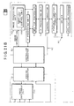
- Figs. 7A and 7B are block diagrams of a hardware configuration in accordance with a first embodiment of the printer of the present invention.
- the hardware of the present invention is constituted by an engine 60 and a controller 62.
- the engine 60 comprises a mechanical controller 64 for performing control actions of the printing mechanisms such as the conveyance belt unit 11 and the electrostatic recording units 24-1 to 24-4 of Fig. 6.
- the mechanical controller 64 is associated with an MPU 66 for sensor processing.
- the MPU 66 for sensor processing receives via AD converters 68-1 and 68-2 a detection signal from the pair of sensors 30-1 and 30-2 arranged below the endless belt 12.
- the mechanical controller 64 is connected to the controller 62 side by way of an engine connector 70.
- the controller 62 comprises an MPU 72.
- an upper apparatus e.g., a personal computer 92 by way of an interface processing unit 74 and a controller connector 76.
- the personal computer 92 includes a driver 96 for performing print processing of color image data fed from an arbitrary application program 94, the driver 96 being connected via a personal computer connector 98 to the controller connector 76 of the controller 62.
- the MPU 72 for controlling controller 62 is associated with image memories 82-1, 82-2, 82-3 and 82-4.
- the MPU 72 converts (i.e. binarizes) image data (gradation pixel data) of Y, M, C and K transferred from the personal computer 92 into binary dot data and deploys them into the image memories 82-1, 82-2, 82-3 and 82-4.
- the MPU 72 includes a quantity-of-light control unit 100 in accordance with the present invention.
- the quantity-of-light control unit 100 For each light-emitting noticeable dot among binarized image dot data, the quantity-of-light control unit 100 figures out a value of optical energy used for the formation of the noticeable dot, on the basis of peripheral dots which may have an influence on the size of the noticeable dot on the record paper. Further, the value of optical energy for light emission control calculated for each dot data is converted into gradation data for light emission driving of each LED chip provided in the LED arrays and then is deployed into the image memories 82-1, 82-2, 82-3 and 82-4. The MPU 72 is able to selectively set either normal mode or optical energy control mode.
- the function of the quantity-of-light control unit 100 is made invalid and the image data (gradation pixel data) of Y, M, C and K are converted into binary dot data and deployed into the image memories 82-1, 82-2, 82-3 and 82-4.
- the function of the quantity-of-light control unit 100 is made valid and image data (gradation pixel data) of Y, M, C and K are converted into binary dot data.
- optical energy of each dot data is calculated, and the thus calculated optical energy is converted into gradation data for light emission driving of the LED chip and is deployed into the image memories 82-1, 82-2, 82-3 and 82-4.
- the selection and setting of the normal mode or the optical energy control mode in the MPU 72 is carried out by the user or the system in compliance with the type of the print images such as letters, photographs and diagrams.
- the MPU 72 is connected to the engine 60 by way of an interface processing unit 78 and a controller connector 80.
- the MPU 72 is provided with an addressing unit 84 for designating addresses when respective color pixel data are deployed into the image memories 82-1 to 82-4.
- the image memories 82-1 to 82-4 are followed by a resolution converting unit 88.
- the resolution converting unit 88 includes buffer memories 90-1, 90-2, 90-3 and 90-4 correspondingly to the Y, M, C and K, respectively.
- the resolution converting unit 88 decomposes pixel data read from the image memories 82-1 to 82-4 in the vertical scanning direction (paper conveyance direction) in the LED arrays 36-1 to 36-4 and converts them into two high-resolution pixel data. If for example the resolution is 600 dpi in the horizontal scanning direction and 600 dpi in the vertical scanning direction upon the deployment into the image memories 82-1 to 82-4, then the resolution converting unit 88 performs a conversion into high-resolution pixel data of 600 dpi in the horizontal scanning direction but of 1800 dpi in the vertical scanning direction.
- Fig. 8 shows the state of arrangement of the LED array for the photosensitive drum provided in the electrostatic recording unit of Fig. 6.
- the LED array 36 consists of a plurality of LED chips 38-1, 38-2, ..., 38-n serving as light emitting elements which are arranged in the horizontal scanning direction orthogonal to the rotational direction of a photosensitive drum 32.
- the pitch of the LED chips 38-1 to 38-n is 42. 3 ⁇ m when the resolution is for example 600 dpi in the horizontal scanning direction.
- the resolution in the vertical scanning direction coincident with the rotational direction of the photosensitive drum 32 depends on the drum peripheral speed.
- the width of the light emission in the drum rotational direction results in 14.1 ⁇ m when the resolution in the vertical scanning direction is for example 1800 dpi.
- Fig. 9 is a function block diagram of the quantity-of-light control unit 100 in accordance with the present invention provided in the MPU 72 for controlling controller 62 of Figs. 7A and 7B.
- the quantity-of-light control unit 100 is provided with a dot data storage unit 102 in the form of a screen buffer, a selection unit 104, an optical energy arithmetic unit 106, an optical energy arithmetic matrix 108, a dot data with optical energy value storage unit 110, and a gradation data conversion unit 112.
- the dot data storage unit 102 stores therein image dot data 116 which are extracted and shown on the right-hand side thereof, obtained by binarizing gradation pixel data of each pixel constituting the image data transmitted from the personal computer 92 side in Figs. 7A and 7B.
- the image dot data 116 include dot data DD11 to DDmn having a pixel size for example of 7680 dots in the horizontal direction and of 5860 dots in the vertical scanning direction.
- the selection unit 104 selects the validity and invalidity of the control function of the quantity-of-light control unit 100. In response to the type of the print image for example, the selection unit 104 selects whether the quantity-of-light control unit 100 is made valid or invalid by the user setting or by the system setting.
- setting of the normal mode invalidates the function of the quantity-of-light control unit 100 whereas setting of the optical energy control mode validates the function of the quantity-of-light control unit 100. More specifically, when the normal mode is selected, the image data 116 placed in the dot data storage unit 102 are intactly deployed into the image memories 90-1 to 90-4 of Fig. 7. On the contrary, when the optical energy control mode is selected, data subjected to processing by the optical energy arithmetic unit 106 and the gradation data conversion unit 112 are deployed into the image memories 90-1 to 90-4 of Figs. 7A and 7B.
- the optical energy arithmetic unit 106 uses the optical energy arithmetic matrix 108 and, every time a light-emitting dot is selected in sequence as a noticeable dot among the image dot data 116, calculates the optical energy for the formation of the noticeable dot on the basis of the peripheral dots which may have an influence on the size of the selected noticeable dot on the record paper. With respect to the optical energy obtained taking into consideration the influence of the peripheral dots on the noticeable dot, the optical energy of the noticeable dot is figured out depending on the distance from the peripheral dots.
- peripheral dots for use in the calculation of the optical energy of the noticeable dot are defined in the optical energy arithmetic matrix 108 and the rate (%) of the optical energy which may have an influence on the noticeable dot due to the light emission of the peripheral dots on the matrix is also defined in the optical energy arithmetic matrix 108.
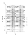
- Fig. 10 is a specific example of the optical energy arithmetic matrix 108 of Fig. 9.
- This optical energy arithmetic matrix 108 represents a print image resolution of 600 dpi in the horizontal scanning direction and of 1800 dpi in the vertical scanning direction, in which case the one dot size Wi in the horizontal scanning direction to be light emission controlled correspondingly to the resolution 600 dpi in the horizontal scanning direction is 42.3 ⁇ m and the one dot size Wj in the vertical scanning direction is 14.1 ⁇ m.
- the 10 has a dot matrix of (5 x 15), that is, in the range of -2 to +2 in the horizontal scanning direction and of -7 to +7 in the vertical scanning direction around a noticeable dot 122.
- This optical energy arithmetic matrix 108 having the size of (5 x 15) previously defines the rate of optical energy which may have an influence on the noticeable dot 122 as the shown percentage values depending on the distance from the noticeable dot.
- the reference optical energy in the optical energy arithmetic matrix 108 is set to 100%.
- the reference optical energy of 100% is defined as the energy posing (causing) no excess exposure in the solid print with respect to the print image having a resolution of 600 dpi in the horizontal scanning direction and of 1800 dpi in the vertical scanning direction.
- an optical energy presenting a maximum value is an optical energy of, e.g., 530% required for the development of isolated one dot having a size corresponding to the resolution of 600 dpi in the horizontal scanning direction and of 1800 dpi in the vertical scanning direction.
- the maximum optical energy capable of being emitted by each of the LED chips 38-1 to 38-n in the LED array 36 of Fig. 8 is for example 280%, and optical energy exceeding 280% is allocated to the adjoining dots for the control of the optical energy.
- Methods of calculating the optical energy for each dot by the optical energy arithmetic unit 106 of Fig. 9 include an addition method and a subtraction method.
- the optical energy arithmetic algorithm by the addition method is as follows.
- the reference value 100% of optical energy to be initially set for the noticeable dot is defined as an optical energy causing no excess exposure in solid print in both the optical energy arithmetic algorithms of the addition method and the subtraction method, although the present invention is not limited to this but the 100% reference optical energy can arbitrarily be defined as an optical energy satisfying appropriate exposure status.
- the maximum value at which the LED can emit light and the value of optical energy of isolated one dot to be initially defined upon the execution of the subtraction method will relatively vary depending on how to determine the reference optical energy 100%.
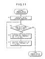
- Fig. 11 is a schematic flowchart of arithmetic processing executed by the optical energy arithmetic unit 106 provided in the quantity-of-light control unit 100 of Fig. 9.
- step S1 binarized image dot data 116 are deployed into the screen buffer in the form of the dot data storage unit 102.
- step S2 in which dot data are fetched in sequence in the order of horizontal scanning direction and the vertical scanning direction and in which check is made to see if calculation for all dots has been completed or not.
- step S3 the procedure goes to step S3 in which the currently fetched i-th dot is defined as a noticeable dot to determine the quantity of the optical energy by the addition method or the subtraction method using the optical energy arithmetic matrix 108. Then in step S4, the quantity of optical energy of the thus determined i-th dot is provided as its output and next dot is again fetched from the screen buffer to repeat the same arithmetic and output of the optical energy. If completion of arithmetic for all the dots is judged in step S2, then the image data conversion processing is complete.
- Fig. 12 is a flowchart of arithmetic processing for determining the optical energy executed in step S3 of Fig. 11, in which the optical energy is calculated by the addition method.
- a reference value L (i1, j1) of the optical energy is defined as 100% in step S1.
- This reference energy 100% is an optical energy posing no excess exposure in solid print for example.
- Procedure then goes to step S2 in which check is made to see if calculation for all dots has been completed or not.
- the dot count to be calculated is 7680 dots in the horizontal scanning direction and 5860 dots in the vertical scanning direction, and hence the counter i1 in the horizontal scanning direction will vary 1 to 7680 and the counter j1 in the vertical scanning direction will vary 1 to 5860.
- the completion of arithmetic of all dots is judged. If the arithmetic of all dots has not yet been completed, procedure goes to step S3 in which a check is made to see if all the areas of the optical energy arithmatic matrix 108 of Fig. 10 have been calculated.
- the positions of dots in the optical energy arithmetic matrix 108 are represented by the horizontal scanning direction i1 and the vertical scanning direction j2, with their respective counters i2 and j2 varying from -2 to +2 and from -7 to 7, respectively, allowing (5 x 15) dots to be subjected to the arithmetic of optical energy. If the entire matrix area has not yet been derived in step S3, then the procedure goes to step S4 in which a check, is made to see if a dot at a position (j1 + j2, j1 + j2) which is obtained by adding the position (i2, j2) of a peripheral dot on the matrix to the position (i1, j1) of the noticeable dot in accordance with the addition algorithm is turned off or not.
- step S5 the optical energy H (i2, j2) of the peripheral dot is added to the optical energy L (i1, j1) of the noticeable dot.
- step S3 such processing is repeated for all the dots in the optical energy arithmetic matrix 108.
- step S2 After the completion of arithmetic for entire matrix area, procedure goes back to step S2 in which the next dot is fetched to repeat the same processing. In this case, upon the return to step S2 after the determination of the optical energy of the noticeable dot, if the thus determined optical energy exceeds the maximum value 280% which the LED can emit, the excess optical energy is allocated to the adjoining underlying dots.
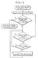
- Fig. 13 is a flowchart of arithmetic processing for determining optical energy in step S3 of Fig. 11, which is characterized in that the optical energy is figured out by the subtraction algorithm.
- Fig. 13 differs from the case of addition algorithm of Fig. 12 in the processing of steps S1, S4 and S5.
- the reference value L(i1, j1) of optical energy is set to 530%.
- step S4 check is made in accordance with the subtraction algorithm to see if a dot at the position (i1 + i2, j1 + j2) which is obtained by adding the position (i2, j2) of a peripheral dot on the matrix to the position (i1, j1) of the noticeable dot is turned off or not.
- step S5 the optical energy H (i2, j2) of the peripheral dot is subtracted from the optical energy L (i1, j1) of the noticeable dot.
- step 3 such processing is repeated for all dots in the optical energy arithmetic matrix 108.
- dot data with the optical energy value calculated by the optical energy arithmetic unit 106 are stored into the dot data with optical energy value storage unit 110.
- the dot data with optical energy value storage unit 110 stores therein dot data DD11 to DDmn and correspondingly thereto optical energy values L11 to Lmn determined as values of quantity-of-light.
- the optical energy value of each dot data calculated by the optical energy arithmetic unit 106 is converted into gradation data of 16 gradationsof the LED chip by the gradation data conversion unit 112 and is stored as image gradation data 120 into a gradation data storage unit 114.
- the gradation data 120 results in gradation data SD11 to SDmn which are represented by e.g., 16 four-bit gradations.
- the gradation data conversion unit 112 converts into a gradation value the optical energy value determined for each dot, the conversion into the gradation value being a conversion which does not present any equi-interval gradation in accordance with the non-linear characteristic.
- Fig. 14 shows the characteristic of conversion from the optical energy into the gradation value, which is executed by the gradation data conversion unit 112 of Fig. 9.
- This conversion characteristic 130 corresponds to the non-linear characteristic of developed dot diameters which are formed correspondingly to the quantity of supply of the optical energy to the photosensitive drum in the electrostatic recording unit of Fig. 8. More specifically, the optical energy of Fig. 14 has equi-interval 16 gradations at 20% increments from 0% to 280%, and correspondingly the developed dot diameters has unequi-interval 16 gradations in accordance with the non-linear characteristic 130.
- 16 four-bit gradations of the LED chip are basically equi-interval, and are unable to provide the unequi-interval gradations corresponding to the dot diameters of Fig. 13.
- the present embodiment provides unequi-interval gradation control for gradating the dot diameters in accordance with the conversion characteristic 130 of Fig. 14, with the quantity of control for driving the light emission of the LED.
- Fig. 15 shows increments of current for controlling the LED light emission drive current in a manner corresponding to the equi-interval gradations of the dot diameters of Fig. 14.
- 0% of turned-off is seen when the optical energy is less than 100%, and hence the light emission drive current values I6 to I16 corresponding to the gradation values of the dot diameters on the vertical axis of Fig. 14 are defined for the gradation values 6, 7, 8, 9, ...16 at 20% increments over 100%.
- Figs. 16A and 16B show other LED drive signals for providing the control of light emission by the unequi-interval gradation values of the present embodiment. These are examples of a strobe control in which pulse trains of the number corresponding to the number of gradations are selectively emitted.
- Fig. 16A shows an ordinary strobe pulse train for use in the equi-interval gradation values. In the case of 16 gradations, 16 pulse timings designated by the gradation values 1 to 16 are prepared so that the pulse trains of the number corresponding to the number of the gradation values are emission driven by the strobe time control.
- the strobe time is controlled so that four pulse trains from the foremost gradation 1 to the gradation 4 are subjected to emission drive. It would be impossible for the strobe pulse having the equi-interval pulse trains of Fig. 16A to provide an emission control corresponding to the unequi-interval gradation values as shown in Fig. 14.
- Fig. 16B there is prepared a strobe pulse train having pulse widths in accordance with the equi-interval gradation values corresponding to the dot diameters.
- This strobe pulse train has a maximum pulse width on the side of the gradation value 1 but has a minimum pulse width on the side of the gradation value 16.
- the strobe time is controlled so as to emission drive the pulse trains of the number corresponding to the unequi-interval gradation values obtained in accordance with the non-linear characteristic 130 of Fig. 14 from the optical energy.
- the above embodiment has employed exposure by the LED array by way of example.
- the optical energy of the emitting dots is controlled by the pulse widths per dots, so that control may be provided so as to ensure that these pulse widths result in pulse widths corresponding to the unequi-interval gradation values in accordance with the non-linear characteristic 130 of Fig. 14.
- the optical energy of emitting dots can be gradation controlled by the number of the light-emitting dots contained in the developed dots.
- the gradation control based on the number of cases where a plurality of exposure dots are positioned within the developed dots, there may be performed the gradation control based on the number of unequi-intervals corresponding to the unequi-interval gradation values in accordance with the non-linear conversion characteristic 130 of Fig. 14 from the optical energy.
- Fig. 17 shows, by way of example of the isolated one dot, a latent image and a developed dot formed by exposure based on the optical energy which has been obtained by the quantity-of-light control unit 100 taking into consideration the influence of light-emission of peripheral dots.
- This isolated one dot is exposed to optical energy 530% of the isolated one dot exposure, with the optical energy posing no excess exposure in solid print being the reference optical energy 100% for example.
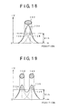
- Fig. 18 shows a latent image and a developed dot formed by two dot line exposure.
- adjoining dots present mutual optical influences, so that as compared with Fig.17 the optical energy is reduced by that influence.
- latent images 126 and 128 indicated by broken lines which do not exceed the threshold value Vth at which dot formation is carried out.
- the resultant combined latent image becomes shown as a latent image 130 indicated by a solid line.
- a developed dot 132 is thus formed which is substantially double the size of the isolated one dot of Fig. 17.
- Fig. 19 shows a case of exposure of two dots with one dot space.
- the optical energy of each dot is reduced as compared with Fig. 18 taking into consideration the mutual optical influences.
- Broken line latent images 134 and 135 are formed by their respective optical energies and a combined latent image is shown as a solid line latent image 136.
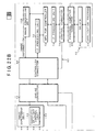
- Figs. 20A and 20B show a second embodiment of the hardware configuration in accordance with the present invention.
- the quantity-of-light control unit 100 of Fig. 9 consists of a first quantity-of-light control unit 100-1 provided in the driver 96 of the personal computer 92 and a second quantity-of-light control unit 100-2 provided in the MPU 72 of the printer associated controller 62.
- the first quantity-of-light control unit 100-1 provided in the driver 96 of the personal computer 92 includes the dot data storage unit 102 in the quantity-of-light control unit 100 of Fig. 9, the selection unit 104, the optical energy arithmetic unit 106, the optical energy arithmetic matrix 108, and the dot data with optical energy value storage unit 110.
- the gradation data conversion unit 112 and the gradation data storage unit 114 are provided in the second quantity-of-light control unit 100-2 of the MPU 72 associated with the printer.
- the entirety of the quantity-of-light control unit 100 of Fig. 9 may be provided in the driver 96 of the personal computer 92.
- the other configuration is the same as that of the first embodiment of Fig. 7.
- Figs. 21A and 21B show a third embodiment of the hardware configuration of the present invention.
- the image memories 82-1 to 82-4 and the resolution converting unit 88 provided in the controller 62 in the first and second embodiments are provided in the engine 60.
- the controller 62 is provided with an image processing unit 150 and the engine 60 is provided with an image deploying unit 160.
- the image processing unit 150 and the image deploying unit 160 share the function of the MPU 72 in the first and second embodiments.
- the quantity-of-light control unit 100 shown in Fig. 9 is provided in the image processing unit 150 of the controller 62.
- Figs. 22A and 22B show a fourth embodiment of the hardware configuration of the present invention, which is characterized in that in the same controller 62 and engine 60 as in the third embodiment hardware configuration of Figs. 21A and 21B, the quantity-of-light control unit 100 of Fig. 9 is provided in the image deploying unit 160 of the engine 60.
- the non-linearity upon the conversion of optical energy into dot diameters in the electrophotographic process is interpolated so that print dots faithful to image dot data can be reproduced. Further, there is no need for a technique using a multiplicity of patterns such as edge recognition for smoothing processing and the like which has hitherto been performed for binarized dot patterns, so that letters, diagrams, images and their mixtures can faithfully be reproduced by means of simplified processing.
- the present invention is not limited to this, but is applicable intactly to an appropriate printer irrespective of whether it is a color printer or a black-and-white printer as long as the printer uses the electrostatic recording units employing an electrophotographic process.
Abstract

Description
- The present invention relates generally to an electrophotographic apparatus and method for use in a printer, a facsimile, etc., in which dot latent images in conformity with binarized image dot data are formed on a photosensitive drum through scanning of an LED array or a laser beam and in which after development of the latent images with toners the resultant dots are transferred onto record paper, and more particularly to an electrophotographic apparatus and method providing control of appropriate quantity of light emission taking into consideration the influence of light from illuminating peripheral dots.
- In the case of conventional electrophotographic apparatuses used for image printing in laser printers, facsimiles or the like, record paper is conveyed at a certain speed by a paper conveyance mechanism so that images are recorded on the record paper through the electrophotographic process executed by electrostatic recording units arranged in the record paper conveyance direction. The electrostatic recording unit forms latent images in conformity with image dot data by means of LED array line scanning or laser diode laser beam scanning on a photosensitive drum in rotation, and after development with toner components, transfers the developed images onto record paper. In recent years, color electrophotographic apparatuses for recording color images have also been put into practice. The color electrophotographic apparatus comprises four electrostatic recording units of black (K), cyan (C), magenta (M) and yellow (Y) in a tandem manner in the record paper conveyance direction. The electrostatic recording units for four colors optically scan the photosensitive drums on the basis of image data to form latent images, develop the latent images with color toners in developing vessels, transfer the developed images onto record paper being conveyed at a certain speed in a superposed manner in the order of yellow (Y), magenta (M), cyan (C) and black (K), and finally perform thermal fixing through a fixing device or other processes.
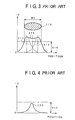
- However, such conventional electrophotographic apparatuses have entailed the following problems since the LED array or the laser diode issues a uniform optical energy per dot to perform development and recording. Now assume that the optical energy has been determined to develop a single isolated dot on a white background. Fig. 1 shows a relationship between a latent image and a bias voltage in the case where the photosensitive drum has been subjected to optical energy capable of developing the single isolated dot in the electrophotographic process. A
latent image 200 is not developed as a toner image at a specific bias voltage Vth or below, but it is developed as atoner image 202 at a voltage exceeding the bias voltage Vth, with the dot size of W1. However, in the case where the optical energy equal to Fig. 1 is supplied to the adjoining two dot positions to develop two dot lines as shown in Fig. 2, latent images 204 and 206 indicated by broken lines are formed for respective dots, resulting in a combinedlatent image 208 indicated by the solid line in its entirety, whereupon atoner image 210 is developed for broken line latent images exceeding the bias voltage Vth. Such a combination of the optical energy supplied to the adjoining dots leads to the dot size W2 exceeding the original two dots. Alternatively, in cases where the optical energy equal to Fig. 1 has been supplied to two dots with one dot space as shown in Fig. 3, the combination oflatent images 212 and 214 indicated by broken lines results in alatent image 216 indicated by a solid line, whereupon atoner image 218 comes to have a three dot size W3 with the crushed intermediate dot. In case of presence of another dot around the illuminated dots in this manner, mutual influence will cause a crush (loss) of the isolated white point when the high-density pattern is printed, with another problem in that halftone pattern of the order of 50% will bring about saturation of density, leading to the density of solid print area. - On the contrary, if the optical energy per dot is determined as shown in Fig. 4 so as to prevent the density of the high-density part from saturating, the
latent image 220 may not reach the bias voltage Vth due to too small optical energy when the one dot isolated point is printed, which makes it impossible to develop the dots. For this reason, respective drawbacks lie in both the method of determining the optical energy so as to enable an individual dot to be developed and the method of determining the optical energy so as to prevent the density of a high-density part from saturating, with the mutual trade-off relationship. Therefore, in reality, an intermediate value of the two methods is employed with their respective problems unsolved. - Further, the drawbacks that the emission of light of a plurality of adjoining dots may cause too large a dot size and that no isolated dot may be formed by the high-density optical energy, will be attributable to the non-linear relationship as shown in Fig. 5, in which the relation between the developed dot diameter and the optical energy is not linear. That is, the dots are not formed with an optical energy L short of a certain threshold value Lth. Once the optical energy exceeds the threshold value Lth, the dot diameter W sharply increases in accordance with the increase of the optical energy P. Afterwards, increase of the dot diameter W gradually reaches a limit along with the increase of the optical energy P.
- According to the present invention, there is provided an electrophotographic apparatus and method capable of faithfully developing and recording dots irrespective of dot patterns, by appropriately controlling optical energy for light-emission taking into consideration the fact that optical energies mutually influence each other between adjacent dots.
- The electrophotographic apparatus of the present invention comprises an electrostatic recording unit and a quantity-of-light control unit. The electrostatic recording unit forms a dot latent image in conformity with binarized image dot data by directing a scanning light beam onto a latent image carrier in motion, e.g., a rotating photosensitive drum arranged in the record paper conveyance direction, and after development with a toner component, transfers dots onto record paper for development. The quantity-of-light control unit controls, for each emitted noticeable dot (visible or discernible dot) in the image data, the optical energy for use in formation of a latent image of the noticeable dot, on the basis of peripheral dots which may have influence on the size of the noticeable dot on the record paper. According to such an electrophotographic apparatus of the present invention, interpolation is made of a non-linear characteristic upon the conversion of the optical energy into dot diameters in the electrophotographic process, thereby achieving a reproduction faithful to the image dot data. Further, there is no need for a technique such as edge recognition for dot pattern smoothing processing and the like, and letters, diagrams, images and their mixtures can faithfully be reproduced. For example, in the case of one dot isolated point, a developed dot of a normal size is obtained from the latent image. In the case of two dot lines, the optical energy is reduced in view of their mutual influence upon the latent image indicated by a broken line (Fig.18). From the combined latent image there is accurately obtained a developed dot having a dot size substantially double the size of one dot.
- The quantity-of-light control unit may control the dot optical energy (beam brightness/duration) in response to the distance from the peripheral dots. For example, as shown by the optical energy arithmetic matrix, the quantity-of-light control unit defines, as a reference value, e.g., a value of 100% of the optical energy of the noticeable dot, as the energy required for formation of a solid part of the record paper on which all dots are transferred. When the peripheral dots are turned off, the optical energy may be defined as the value obtained by adding to the
reference value 100%, the quantity of optical energy which has been compensated for by light-emission of the peripheral dots, in other words, a light level of a percentage which is defined in the optical energy arithmetic matrix. - An alternative is to define, as a reference value of optical energy of the noticeable dot, an optical energy,e.g. of 530% required for development of an isolated point. The quantity-of-light control unit, when the peripheral dots are turned on, controls the optical energy to be equal to a value obtained by subtracting from the
reference value 530% the quantity of optical energy which has been compensated for by light-emission of the peripheral dots. - In an embodiment, when the value of optical energy for controlling the noticeable dot exceeds the maximum value, e.g., 280% capable of being controlled per dot by the electrostatic recording unit, the optical energy is controlled so as to allocate the quantity of optical energy exceeding the
maximum value 280% to adjoining dots. - Alternatively, when the above value of optical energy exceeds the
maximum value 280% capable of being controlled per dot by the electrostatic recording unit, output of optical energy may be provided discretely through a plurality of scanning operations. - Preferably, the optical energy is controlled so that the noticeable dot forms one dot isolated point. Also, the optical energy of the noticeable dot preferably is set so that the density is not saturated with a high-density region. When using an LED array in said electrostatic recording unit, the optical energy of illuminated dots can be controlled by varying the strobe time of a pulse train issued from LED elements.
- Alternatively, it can be controlled by varying the quantity of light-emission per unit time of the LED elements.
- When a laser beam is employed as the scanning beam in the electrostatic recording unit, the dot optical energy can be controlled by the pulse width per dot.
- When using an LED array which is controlled by converting the optical energy of illuminated dots into gradation values, it is preferable to convert the optical energy into gradation values in such a manner that the gradation values have no equi-intervals (linearity). For example, the quantity-of-light control unit, when control is provided by converting said gradation values into a strobe time of a pulse train issued from the LED elements, performs conversion in such a manner that the pulse widths of the pulse train as a result of conversion of the gradation values have no equi-intervals.
- In the case of converting the gradation values into a drive current of the LED elements, the conversion may be done in such a manner that a drive current of the LED elements which is obtained by converting the gradation values has no equi-interval increments.
- When the size of exposed dots in an exposure system is smaller than the size of developed dots formed on the record paper by the electrostatic recording unit, the optical energy of illuminated dots can be controlled by the number of exposed dots contained in each developed dot.
- In the electrophotographic apparatus of the present invention, the quantity-of-light control unit may be subjected to selective control and non-control.
- Further, the present invention provides an electrophotographic method comprising an electrostatic recording step in which dot latent images in conformity with image dot data are formed by directing a scanning beam onto a latent image carrier in motion, e.g., a rotating photosensitive drum arranged in the record paper conveyance direction and in which after developing with a toner component, dots are transferred onto the record paper for development; and a quantity-of-light control step in which for each noticeable dot (visible or discernible dot lit up by the beam) among the image dot data, optical energy for use in formation of the noticeable dot is controlled for output, on the basis of peripheral dots which may have influence on the size of the noticeable dot on the record paper.
- A detailed description will now be given, by way of example, with reference to the accompanying drawings, in which:
- Fig. 1 is an explanatory diagram of a latent image and the dot size of a conventional one dot line;
- Fig. 2 is an explanatory diagram of latent images and the dot size of conventional two dot lines;
- Fig. 3 is an explanatory diagram of latent images and the dot size of a conventional two dot emission with one dot space;
- Fig. 4 is an explanatory diagram of a latent image and the dot size of one dot line obtained when optical energy is combined with conventional high-density development;
- Fig. 5 is a non-linear characteristic diagram of the optical energy and the dot diameter in the electrophotographic process;
- Fig. 6 is an explanatory diagram of an internal structure of the apparatus body of the present invention;
- Figs. 7A and 7B are explanatory diagrams of a hardware configuration in accordance with a first embodiment of the present invention;
- Fig. 8 is an explanatory diagram of a photosensitive drum and an LED array of an electrostatic recording unit;
- Fig. 9 is a function block diagram of a current control unit of the present invention;
- Fig. 10 is an explanatory diagram of an optical energy arithmetic matrix for use in calculation of optical energy of Fig. 9;
- Fig. 11 is a flowchart of image data conversion processing of the present invention;
- Fig. 12 is a flowchart of the optical energy arithmetic processing of Fig. 10 in accordance with the addition method;
- Fig. 13 is a flowchart of the optical energy arithmetic processing of Fig. 10 in accordance with the subtraction method;
- Fig. 14 is an explanatory diagram of conversion from optical energy into gradation values in Fig. 9;
- Fig. 15 is an explanatory diagram of conversion of LED light-emission current in accordance with Fig. 13;
- Figs. 16A and 16B are explanatory diagrams of conversion of pulse train strobe time in accordance with Fig. 13;
- Fig. 17 is an explanatory diagram of a latent image and the dot size of one dot line in accordance with the present invention;
- Fig. 18 is an explanatory diagram of latent images and the dot size of two dot lines in accordance with the present invention;
- Fig. 19 is an explanatory diagram of a latent image and the dot size of two dot emission with one dot space in accordance with the present invention;
- Figs. 20A and 20B are block diagrams of a hardware configuration in accordance with a second embodiment of the present invention;
- Figs. 21A and 21B are block diagrams of a hardware configuration in accordance with a third embodiment of the present invention; and
- Figs. 22A and 22B are block diagrams of a hardware configuration in accordance with a fourth embodiment of the present invention.
-
- Fig. 6 illustrates an internal structure of an electrophotographic apparatus of the present invention in the form of a printer by way of example. An
apparatus body 10 accommodates therein aconveyance belt unit 11 for conveying record media, e.g., record sheets of paper. Theconveyance belt unit 11 is provided rotationally with anendless belt 12 made of a transmittable dielectric material, e.g., a suitable synthetic resin material. Theendless belt 12 extends around four rollers 22-1, 22-2, 22-3 and 22-4. Theconveyance belt unit 11 is removably mounted to theapparatus body 10. The roller 22-1 functions as a driving roller. The driving roller 22-1 connects via a gear train not shown to abelt motor 25 so as to cause theendless belt 12 to run at a certain speed in the clockwise direction indicated by an arrow. The drive roller 22-1 functions also as an AC elimination roller for eliminating electric charge from theendless belt 12. The roller 22-2 acts as a driven roller. The driven roller 22-2 acts also as a charging roller for imparting electric charge to theendless belt 12. The rollers 22-3 and 22-4 serve as guide rollers and are arranged in the vicinity of the driving roller 22-1 and the driven roller 22-2, respectively. An upper running part of theendless belt 12 between the driven roller 22-2 and the driving roller 22-1 forms a moving path for the record sheets of paper. The record sheets of paper are stacked in ahopper 14 and are picked up one by one from the topmost record sheet of paper in thehopper 14 by means of apickup roller 16. The record paper then passes through a recordpaper guide passage 18 and is led by a pair of recordpaper feeding rollers 20 from the driven roller 22-2 sideendless belt 12 onto the record paper moving path on the belt upper side. After having passed through the record paper moving path, the record paper is discharged from the drive roller 22-1. Since theendless belt 12 is charged by the driven roller 22-2, the record paper electrostatically adheres to theendless belt 12 when it is led from the driven roller 22-2 onto the record paper moving path, so that the record paper in motion is prevented from being positionally offset. On the other hand, the driving roller 22-1 on the discharge side serves as a charge eliminating roller, so that theendless belt 12 is cleared of electric charge at the region where theendless belt 12 comes into contact with the driving roller 22-1. For this reason, the record paper is cleared of electric charge when it passes through the driving roller 22-1, with the result that it is easily separated and discharged from theendless belt 12 without being caught by the lower belt part. Theapparatus body 10 accommodates therein four electrostatic recording units 24-1, 24-2, 24-3 and 24-4 for Y, M, C and K, which are arranged in series, i.e., in a tandem manner from upstream toward downstream in the mentioned order along the record paper moving path on the upper side of theendless belt 12 defined between the driven roller 22-2 and the driving roller 22-1. The electrostatic recording units 24-1 to 24-4 are equipped with drum motors 15-1 to 15-4 for driving photosensitive drums and have substantially the same structure except that developing agents used are a yellow toner component (Y), a magenta toner component (M), a cyan toner component (C) and a black toner component (K), respectively. For this reason, the electrostatic recording units 24-1 to 24-4 transfer and record a yellow toner image, a magenta toner image, a cyan toner image and a black toner image onto the record paper moving along the record paper moving path on the upper side of theendless belt 12, in sequence and in a superposed manner, to form a full-color toner image. Furthermore, in the case of the present invention, adjustment is made so that amounts of consumption of the color toner components in the electrostatic recording units 24-1 to 24-4 are substantially the same. While the record paper passes through the record paper moving path on theendless belt 12 defined between the driven roller 22-2 and the driving roller 22-1, it is subjected to transfer and superposition of the four color toner images of Y, M, C and K by the electrostatic recording units 24-1 to 24-4 and comes to have a full-color image formed thereon. The record paper is then delivered from the driving roller 22-1 side toward a heat roller typethermal fixing device 26 to perform a thermal fixation of the full-color image on the record paper. After the completion of the thermal fixation, the record paper passes through the guide rollers and enters astacker 28 provided above the apparatus body for stacking the record paper therein. Confronting the lower belt surface of theendless belt 12, there are arranged a pair of sensors 30-1 and 30-2 in the direction orthogonal to the belt moving direction, with only the sensor 30-1 closer to the viewer being visible. The sensors 30-1 and 30-2 are used to optically read a toner mark transferred onto theendless belt 12 to thereby correct the amount of a positional offset. - Figs. 7A and 7B are block diagrams of a hardware configuration in accordance with a first embodiment of the printer of the present invention. The hardware of the present invention is constituted by an
engine 60 and acontroller 62. Theengine 60 comprises a mechanical controller 64 for performing control actions of the printing mechanisms such as theconveyance belt unit 11 and the electrostatic recording units 24-1 to 24-4 of Fig. 6. The mechanical controller 64 is associated with anMPU 66 for sensor processing. TheMPU 66 for sensor processing receives via AD converters 68-1 and 68-2 a detection signal from the pair of sensors 30-1 and 30-2 arranged below theendless belt 12. The mechanical controller 64 is connected to thecontroller 62 side by way of anengine connector 70. Herein, the printing mechanisms provided in theengine 60 are shown to exclusively include theendless belt 12 and LED arrays 36-1, 36-2, 36-3 and 36-4 provided on the electrostatic recording units of Y, M, C and K, respectively. Thecontroller 62 comprises anMPU 72. To theMPU 72 ofcontroller 62 is connected an upper apparatus, e.g., apersonal computer 92 by way of aninterface processing unit 74 and a controller connector 76. Thepersonal computer 92 includes adriver 96 for performing print processing of color image data fed from anarbitrary application program 94, thedriver 96 being connected via apersonal computer connector 98 to the controller connector 76 of thecontroller 62. TheMPU 72 for controllingcontroller 62 is associated with image memories 82-1, 82-2, 82-3 and 82-4. TheMPU 72 converts (i.e. binarizes) image data (gradation pixel data) of Y, M, C and K transferred from thepersonal computer 92 into binary dot data and deploys them into the image memories 82-1, 82-2, 82-3 and 82-4. - In this first embodiment, the
MPU 72 includes a quantity-of-light control unit 100 in accordance with the present invention. For each light-emitting noticeable dot among binarized image dot data, the quantity-of-light control unit 100 figures out a value of optical energy used for the formation of the noticeable dot, on the basis of peripheral dots which may have an influence on the size of the noticeable dot on the record paper. Further, the value of optical energy for light emission control calculated for each dot data is converted into gradation data for light emission driving of each LED chip provided in the LED arrays and then is deployed into the image memories 82-1, 82-2, 82-3 and 82-4. TheMPU 72 is able to selectively set either normal mode or optical energy control mode. When the normal mode is selected, the function of the quantity-of-light control unit 100 is made invalid and the image data (gradation pixel data) of Y, M, C and K are converted into binary dot data and deployed into the image memories 82-1, 82-2, 82-3 and 82-4. On the contrary, when the optical energy control mode is selected, the function of the quantity-of-light control unit 100 is made valid and image data (gradation pixel data) of Y, M, C and K are converted into binary dot data. Afterward, optical energy of each dot data is calculated, and the thus calculated optical energy is converted into gradation data for light emission driving of the LED chip and is deployed into the image memories 82-1, 82-2, 82-3 and 82-4. The selection and setting of the normal mode or the optical energy control mode in theMPU 72 is carried out by the user or the system in compliance with the type of the print images such as letters, photographs and diagrams. TheMPU 72 is connected to theengine 60 by way of aninterface processing unit 78 and acontroller connector 80. TheMPU 72 is provided with an addressing unit 84 for designating addresses when respective color pixel data are deployed into the image memories 82-1 to 82-4. The image memories 82-1 to 82-4 are followed by aresolution converting unit 88. Theresolution converting unit 88 includes buffer memories 90-1, 90-2, 90-3 and 90-4 correspondingly to the Y, M, C and K, respectively. Theresolution converting unit 88 decomposes pixel data read from the image memories 82-1 to 82-4 in the vertical scanning direction (paper conveyance direction) in the LED arrays 36-1 to 36-4 and converts them into two high-resolution pixel data. If for example the resolution is 600 dpi in the horizontal scanning direction and 600 dpi in the vertical scanning direction upon the deployment into the image memories 82-1 to 82-4, then theresolution converting unit 88 performs a conversion into high-resolution pixel data of 600 dpi in the horizontal scanning direction but of 1800 dpi in the vertical scanning direction. - Fig. 8 shows the state of arrangement of the LED array for the photosensitive drum provided in the electrostatic recording unit of Fig. 6. The
LED array 36 consists of a plurality of LED chips 38-1, 38-2, ..., 38-n serving as light emitting elements which are arranged in the horizontal scanning direction orthogonal to the rotational direction of aphotosensitive drum 32. The pitch of the LED chips 38-1 to 38-n is 42. 3 µm when the resolution is for example 600 dpi in the horizontal scanning direction. Further, the resolution in the vertical scanning direction coincident with the rotational direction of thephotosensitive drum 32 depends on the drum peripheral speed. The width of the light emission in the drum rotational direction results in 14.1 µm when the resolution in the vertical scanning direction is for example 1800 dpi. - Fig. 9 is a function block diagram of the quantity-of-
light control unit 100 in accordance with the present invention provided in theMPU 72 for controllingcontroller 62 of Figs. 7A and 7B. The quantity-of-light control unit 100 is provided with a dotdata storage unit 102 in the form of a screen buffer, a selection unit 104, an optical energy arithmetic unit 106, an opticalenergy arithmetic matrix 108, a dot data with optical energy value storage unit 110, and a gradationdata conversion unit 112. The dotdata storage unit 102 stores thereinimage dot data 116 which are extracted and shown on the right-hand side thereof, obtained by binarizing gradation pixel data of each pixel constituting the image data transmitted from thepersonal computer 92 side in Figs. 7A and 7B. Theimage dot data 116 include dot data DD11 to DDmn having a pixel size for example of 7680 dots in the horizontal direction and of 5860 dots in the vertical scanning direction. The selection unit 104 selects the validity and invalidity of the control function of the quantity-of-light control unit 100. In response to the type of the print image for example, the selection unit 104 selects whether the quantity-of-light control unit 100 is made valid or invalid by the user setting or by the system setting. In this selection, as set forth with respect to theMPU 72 of Figs. 7A and 7B, setting of the normal mode invalidates the function of the quantity-of-light control unit 100 whereas setting of the optical energy control mode validates the function of the quantity-of-light control unit 100. More specifically, when the normal mode is selected, theimage data 116 placed in the dotdata storage unit 102 are intactly deployed into the image memories 90-1 to 90-4 of Fig. 7. On the contrary, when the optical energy control mode is selected, data subjected to processing by the optical energy arithmetic unit 106 and the gradationdata conversion unit 112 are deployed into the image memories 90-1 to 90-4 of Figs. 7A and 7B. The optical energy arithmetic unit 106 uses the opticalenergy arithmetic matrix 108 and, every time a light-emitting dot is selected in sequence as a noticeable dot among theimage dot data 116, calculates the optical energy for the formation of the noticeable dot on the basis of the peripheral dots which may have an influence on the size of the selected noticeable dot on the record paper. With respect to the optical energy obtained taking into consideration the influence of the peripheral dots on the noticeable dot, the optical energy of the noticeable dot is figured out depending on the distance from the peripheral dots. The peripheral dots for use in the calculation of the optical energy of the noticeable dot are defined in the opticalenergy arithmetic matrix 108 and the rate (%) of the optical energy which may have an influence on the noticeable dot due to the light emission of the peripheral dots on the matrix is also defined in the opticalenergy arithmetic matrix 108. - Fig. 10 is a specific example of the optical
energy arithmetic matrix 108 of Fig. 9. This opticalenergy arithmetic matrix 108 represents a print image resolution of 600 dpi in the horizontal scanning direction and of 1800 dpi in the vertical scanning direction, in which case the one dot size Wi in the horizontal scanning direction to be light emission controlled correspondingly to the resolution 600 dpi in the horizontal scanning direction is 42.3 µm and the one dot size Wj in the vertical scanning direction is 14.1µm. In a manner corresponding to such a print image resolution, the opticalenergy arithmetic matrix 108 of Fig. 10 has a dot matrix of (5 x 15), that is, in the range of -2 to +2 in the horizontal scanning direction and of -7 to +7 in the vertical scanning direction around anoticeable dot 122. This opticalenergy arithmetic matrix 108 having the size of (5 x 15) previously defines the rate of optical energy which may have an influence on thenoticeable dot 122 as the shown percentage values depending on the distance from the noticeable dot. In this case, the reference optical energy in the opticalenergy arithmetic matrix 108 is set to 100%. The reference optical energy of 100% is defined as the energy posing (causing) no excess exposure in the solid print with respect to the print image having a resolution of 600 dpi in the horizontal scanning direction and of 1800 dpi in the vertical scanning direction. In response to this, defined as an optical energy presenting a maximum value is an optical energy of, e.g., 530% required for the development of isolated one dot having a size corresponding to the resolution of 600 dpi in the horizontal scanning direction and of 1800 dpi in the vertical scanning direction. Further, the maximum optical energy capable of being emitted by each of the LED chips 38-1 to 38-n in theLED array 36 of Fig. 8 is for example 280%, and optical energy exceeding 280% is allocated to the adjoining dots for the control of the optical energy. - Methods of calculating the optical energy for each dot by the optical energy arithmetic unit 106 of Fig. 9 include an addition method and a subtraction method. The optical energy arithmetic algorithm by the addition method is as follows.
-
- I) Determine a reference
optical energy 100%. Define as the referenceoptical energy 100% an optical energy posing no excess exposure in solid print. - II) Select an arbitrary noticeable dot. If
the noticeable dot is a light-emitting dot, assume that
the optical energy of the noticeable dot is the
reference
optical energy 100%. - III) Using the optical
energy arithmetic matrix 108 of Fig. 10, select non-light-emitting peripheral dots from the peripheral dots of thenoticeable dot 122 and add the optical energies defined for the non-light-emitting peripheral dots to thenoticeable dot 122. If for example there exist three dots having coordinates (1, -1), (0, 1), (0, -2) indicated by meshes as the peripheral dots, the degrees of influence of the respective optical energies are 6%, 170% and 40%, and hence these are added to the reference optical energy which has initially been set for thenoticeable dot 112 to obtain - IV) The LED chip of this embodiment is
capable of light-emitting in 16 gradations in four bits
and the gradation values are defined at every 20% from
0% (turned off) and 100% up to 280% upon lighting, over
which there goes the optical energy 316% which is the
value obtained by calculating the maximum light-emitting
energy 280% with respect to the noticeable dot. Therefore, the excess 36% of the optical energy 316% calculated for the definition of themaximum value 280% is added to the calculation of the underlying dots adjoining thenoticeable dot 112. - V) Such optical energy calculation is carried out for all the dots to determine the optical energies of the light-emitting dots.
-
- Following is the description of the optical energy arithmetic algorithm in accordance with the subtraction method.
-
- I) Determine a reference optical energy.
Define as the reference optical energy an
optical energy 100% causing no excess exposure in solid print in the same manner as the addition method. - II) Select an arbitrary light-emitting dot
as a noticeable dot and assume that the optical energy
of the noticeable dot is
optical energy 530% which is required for the development of isolated one dot. - III) Using the optical
energy arithmetic matrix 108 of Fig. 10, examine light-emitting dots in the peripheral dots of thenoticeable dot 122 and subtract the values of the light-emitting dots defined on the matrix from the noticeable dot. If for example three dots having coordinates (1, -1), (0, 1), (0, -1) indicated by meshes around thenoticeable dot 122 of the opticalenergy arithmetic matrix 108 of Fig. 10 emit light, optical energies of the respective light-emitting peripheral dots are 6%, 170% and 40%, and hence the optical energy of thenoticeable dot 122 is given as - IV) The LED chip of the present invention
is capable of light-emitting in 16 gradations in four
bits and the gradation values are defined at every 20%
from 0% (turned off) and 100% up to 280% upon illumination.
The optical energy 184% calculated for the
noticeable dot 122 results in an optical energy of 180% gradation by rounding off. If the optical energy of thenoticeable dot 122 obtained by the subtraction goes over themaximum value 280% of the LED chip, then the excess optical energy is added to the calculation of the adjoining underlying dots. - V) Such processing is carried out for all the dots to determine the optical energies of the light-emitting dots.
-
- In this case, the
reference value 100% of optical energy to be initially set for the noticeable dot is defined as an optical energy causing no excess exposure in solid print in both the optical energy arithmetic algorithms of the addition method and the subtraction method, although the present invention is not limited to this but the 100% reference optical energy can arbitrarily be defined as an optical energy satisfying appropriate exposure status. By defining an appropriate referenceoptical energy 100% in this manner, the maximum value at which the LED can emit light and the value of optical energy of isolated one dot to be initially defined upon the execution of the subtraction method will relatively vary depending on how to determine the referenceoptical energy 100%. - Fig. 11 is a schematic flowchart of arithmetic processing executed by the optical energy arithmetic unit 106 provided in the quantity-of-
light control unit 100 of Fig. 9. First in step S1, binarizedimage dot data 116 are deployed into the screen buffer in the form of the dotdata storage unit 102. Then procedure goes to step S2 in which dot data are fetched in sequence in the order of horizontal scanning direction and the vertical scanning direction and in which check is made to see if calculation for all dots has been completed or not. If not, then the procedure goes to step S3 in which the currently fetched i-th dot is defined as a noticeable dot to determine the quantity of the optical energy by the addition method or the subtraction method using the opticalenergy arithmetic matrix 108. Then in step S4, the quantity of optical energy of the thus determined i-th dot is provided as its output and next dot is again fetched from the screen buffer to repeat the same arithmetic and output of the optical energy. If completion of arithmetic for all the dots is judged in step S2, then the image data conversion processing is complete. - Fig. 12 is a flowchart of arithmetic processing for determining the optical energy executed in step S3 of Fig. 11, in which the optical energy is calculated by the addition method. On starting arithmetic of the optical energy of an arbitrary noticeable dot (i1, j1), a reference value L (i1, j1) of the optical energy is defined as 100% in step S1. This
reference energy 100% is an optical energy posing no excess exposure in solid print for example. Procedure then goes to step S2 in which check is made to see if calculation for all dots has been completed or not. In this embodiment, the dot count to be calculated is 7680 dots in the horizontal scanning direction and 5860 dots in the vertical scanning direction, and hence the counter i1 in the horizontal scanning direction will vary 1 to 7680 and the counter j1 in the vertical scanning direction will vary 1 to 5860. Thus when i1 = 7680 and j1 = 5860 are exceeded, the completion of arithmetic of all dots is judged. If the arithmetic of all dots has not yet been completed, procedure goes to step S3 in which a check is made to see if all the areas of the opticalenergy arithmatic matrix 108 of Fig. 10 have been calculated. The positions of dots in the opticalenergy arithmetic matrix 108 are represented by the horizontal scanning direction i1 and the vertical scanning direction j2, with their respective counters i2 and j2 varying from -2 to +2 and from -7 to 7, respectively, allowing (5 x 15) dots to be subjected to the arithmetic of optical energy. If the entire matrix area has not yet been derived in step S3, then the procedure goes to step S4 in which a check, is made to see if a dot at a position (j1 + j2, j1 + j2) which is obtained by adding the position (i2, j2) of a peripheral dot on the matrix to the position (i1, j1) of the noticeable dot in accordance with the addition algorithm is turned off or not. If it is lit, the arithmetic of optical energy is not carried out. If it is turned off, procedure goes to step S5 in which the optical energy H (i2, j2) of the peripheral dot is added to the optical energy L (i1, j1) of the noticeable dot. In step S3, such processing is repeated for all the dots in the opticalenergy arithmetic matrix 108. After the completion of arithmetic for entire matrix area, procedure goes back to step S2 in which the next dot is fetched to repeat the same processing. In this case, upon the return to step S2 after the determination of the optical energy of the noticeable dot, if the thus determined optical energy exceeds themaximum value 280% which the LED can emit, the excess optical energy is allocated to the adjoining underlying dots. For this reason, in the arithmetic of optical energy of the succeeding dot which has received allocation of optical energy from the preceding dot, the addition of energy due to turn-off of the peripheral pixels is carried out to the initial value which is the sum ofreference energy 100% and the excess optical energy subjected to allocation. - Fig. 13 is a flowchart of arithmetic processing for determining optical energy in step S3 of Fig. 11, which is characterized in that the optical energy is figured out by the subtraction algorithm. Fig. 13 differs from the case of addition algorithm of Fig. 12 in the processing of steps S1, S4 and S5. First in step S1, the reference value L(i1, j1) of optical energy is set to 530%. In step S4, check is made in accordance with the subtraction algorithm to see if a dot at the position (i1 + i2, j1 + j2) which is obtained by adding the position (i2, j2) of a peripheral dot on the matrix to the position (i1, j1) of the noticeable dot is turned off or not. If it is tuned off, no arithmetic of the optical energy is carried out. If it is turned on, the procedure goes to step S5 in which the optical energy H (i2, j2) of the peripheral dot is subtracted from the optical energy L (i1, j1) of the noticeable dot. In
step 3, such processing is repeated for all dots in the opticalenergy arithmetic matrix 108. - Referring again to Fig. 9, dot data with the optical energy value calculated by the optical energy arithmetic unit 106 are stored into the dot data with optical energy value storage unit 110. As shown solely on the right-hand side, the dot data with optical energy value storage unit 110 stores therein dot data DD11 to DDmn and correspondingly thereto optical energy values L11 to Lmn determined as values of quantity-of-light. Then the optical energy value of each dot data calculated by the optical energy arithmetic unit 106 is converted into gradation data of 16 gradationsof the LED chip by the gradation
data conversion unit 112 and is stored asimage gradation data 120 into a gradationdata storage unit 114. Thegradation data 120 results in gradation data SD11 to SDmn which are represented by e.g., 16 four-bit gradations. The gradationdata conversion unit 112 converts into a gradation value the optical energy value determined for each dot, the conversion into the gradation value being a conversion which does not present any equi-interval gradation in accordance with the non-linear characteristic. - Fig. 14 shows the characteristic of conversion from the optical energy into the gradation value, which is executed by the gradation
data conversion unit 112 of Fig. 9. This conversion characteristic 130 corresponds to the non-linear characteristic of developed dot diameters which are formed correspondingly to the quantity of supply of the optical energy to the photosensitive drum in the electrostatic recording unit of Fig. 8. More specifically, the optical energy of Fig. 14 has equi-interval 16 gradations at 20% increments from 0% to 280%, and correspondingly the developed dot diameters has unequi-interval 16 gradations in accordance with thenon-linear characteristic 130. On the contrary, 16 four-bit gradations of the LED chip are basically equi-interval, and are unable to provide the unequi-interval gradations corresponding to the dot diameters of Fig. 13. Thus, the present embodiment provides unequi-interval gradation control for gradating the dot diameters in accordance with theconversion characteristic 130 of Fig. 14, with the quantity of control for driving the light emission of the LED. - Fig. 15 shows increments of current for controlling the LED light emission drive current in a manner corresponding to the equi-interval gradations of the dot diameters of Fig. 14. In the present embodiment, 0% of turned-off is seen when the optical energy is less than 100%, and hence the light emission drive current values I6 to I16 corresponding to the gradation values of the dot diameters on the vertical axis of Fig. 14 are defined for the gradation values 6, 7, 8, 9, ...16 at 20% increments over 100%.
- Figs. 16A and 16B show other LED drive signals for providing the control of light emission by the unequi-interval gradation values of the present embodiment. These are examples of a strobe control in which pulse trains of the number corresponding to the number of gradations are selectively emitted. Fig. 16A shows an ordinary strobe pulse train for use in the equi-interval gradation values. In the case of 16 gradations, 16 pulse timings designated by the gradation values 1 to 16 are prepared so that the pulse trains of the number corresponding to the number of the gradation values are emission driven by the strobe time control. For example, in case of the
gradation value 4, the strobe time is controlled so that four pulse trains from theforemost gradation 1 to thegradation 4 are subjected to emission drive. It would be impossible for the strobe pulse having the equi-interval pulse trains of Fig. 16A to provide an emission control corresponding to the unequi-interval gradation values as shown in Fig. 14. Thus, as shown in Fig. 16B, there is prepared a strobe pulse train having pulse widths in accordance with the equi-interval gradation values corresponding to the dot diameters. This strobe pulse train has a maximum pulse width on the side of thegradation value 1 but has a minimum pulse width on the side of thegradation value 16. Then the strobe time is controlled so as to emission drive the pulse trains of the number corresponding to the unequi-interval gradation values obtained in accordance with thenon-linear characteristic 130 of Fig. 14 from the optical energy. - The above embodiment has employed exposure by the LED array by way of example. However, in the case of the electrostatic recording unit in which a laser beam from laser diodes in place of the LEDs is scanned in the direction orthogonal to the rotational direction of the photosensitive drum, the optical energy of the emitting dots is controlled by the pulse widths per dots, so that control may be provided so as to ensure that these pulse widths result in pulse widths corresponding to the unequi-interval gradation values in accordance with the
non-linear characteristic 130 of Fig. 14. Further, in case the dot size of the exposure system by the electrostatic developing unit is smaller than the dot size developed on the record paper, the optical energy of emitting dots can be gradation controlled by the number of the light-emitting dots contained in the developed dots. In this manner, also as to the gradation control based on the number of cases where a plurality of exposure dots are positioned within the developed dots, there may be performed the gradation control based on the number of unequi-intervals corresponding to the unequi-interval gradation values in accordance with thenon-linear conversion characteristic 130 of Fig. 14 from the optical energy. - Fig. 17 shows, by way of example of the isolated one dot, a latent image and a developed dot formed by exposure based on the optical energy which has been obtained by the quantity-of-
light control unit 100 taking into consideration the influence of light-emission of peripheral dots. This isolated one dot is exposed tooptical energy 530% of the isolated one dot exposure, with the optical energy posing no excess exposure in solid print being the referenceoptical energy 100% for example. In this case, there is obtained adeveloped dot 124 of normal size in a manner corresponding to alatent image 122 exceeding a threshold value Vth with respect to the bias voltage-V. - Fig. 18 shows a latent image and a developed dot formed by two dot line exposure. In the case of the two dot lines, adjoining dots present mutual optical influences, so that as compared with Fig.17 the optical energy is reduced by that influence. As a result, there are formed latent images 126 and 128 indicated by broken lines which do not exceed the threshold value Vth at which dot formation is carried out. The resultant combined latent image becomes shown as a
latent image 130 indicated by a solid line. Adeveloped dot 132 is thus formed which is substantially double the size of the isolated one dot of Fig. 17. - Fig. 19 shows a case of exposure of two dots with one dot space. In this case as well, the optical energy of each dot is reduced as compared with Fig. 18 taking into consideration the mutual optical influences. Broken line latent images 134 and 135 are formed by their respective optical energies and a combined latent image is shown as a solid line
latent image 136. As a result of this, there can be formed developeddots 138 and 140 of substantially the same size as the isolated one dot of Fig. 18 correspondingly to the part of the latent image exceeding the threshold value Vth. - Figs. 20A and 20B show a second embodiment of the hardware configuration in accordance with the present invention. This embodiment is characterized in that the quantity-of-
light control unit 100 of Fig. 9 consists of a first quantity-of-light control unit 100-1 provided in thedriver 96 of thepersonal computer 92 and a second quantity-of-light control unit 100-2 provided in theMPU 72 of the printer associatedcontroller 62. The first quantity-of-light control unit 100-1 provided in thedriver 96 of thepersonal computer 92 includes the dotdata storage unit 102 in the quantity-of-light control unit 100 of Fig. 9, the selection unit 104, the optical energy arithmetic unit 106, the opticalenergy arithmetic matrix 108, and the dot data with optical energy value storage unit 110. On the contrary, the gradationdata conversion unit 112 and the gradationdata storage unit 114 are provided in the second quantity-of-light control unit 100-2 of theMPU 72 associated with the printer. - Naturally, the entirety of the quantity-of-
light control unit 100 of Fig. 9 may be provided in thedriver 96 of thepersonal computer 92. The other configuration is the same as that of the first embodiment of Fig. 7. - Figs. 21A and 21B show a third embodiment of the hardware configuration of the present invention. In the third embodiment, the image memories 82-1 to 82-4 and the
resolution converting unit 88 provided in thecontroller 62 in the first and second embodiments are provided in theengine 60. Correspondingly, thecontroller 62 is provided with animage processing unit 150 and theengine 60 is provided with animage deploying unit 160. Theimage processing unit 150 and theimage deploying unit 160 share the function of theMPU 72 in the first and second embodiments. In the third embodiment of Figs. 21A and 21B, the quantity-of-light control unit 100 shown in Fig. 9 is provided in theimage processing unit 150 of thecontroller 62. - Figs. 22A and 22B show a fourth embodiment of the hardware configuration of the present invention, which is characterized in that in the
same controller 62 andengine 60 as in the third embodiment hardware configuration of Figs. 21A and 21B, the quantity-of-light control unit 100 of Fig. 9 is provided in theimage deploying unit 160 of theengine 60. - According to the present invention as set forth hereinabove, the non-linearity upon the conversion of optical energy into dot diameters in the electrophotographic process is interpolated so that print dots faithful to image dot data can be reproduced. Further, there is no need for a technique using a multiplicity of patterns such as edge recognition for smoothing processing and the like which has hitherto been performed for binarized dot patterns, so that letters, diagrams, images and their mixtures can faithfully be reproduced by means of simplified processing.
- Although in the above embodiments description has been made, by way of example, of the color printer having the electrostatic recording units 24-1 to 24-4 of yellow, magenta, cyan and black which are arranged along the conveyance belt in a tandem manner, the present invention is not limited to this, but is applicable intactly to an appropriate printer irrespective of whether it is a color printer or a black-and-white printer as long as the printer uses the electrostatic recording units employing an electrophotographic process.
- Although the above embodiments have been related to the printer by way of example, the present invention is applicable intactly to other electrophotographic apparatuses such as facsimiles which record images on appropriate sheet media.
Claims (17)
- An electrophotographic apparatus comprising:an electrostatic recording unit which forms a dot latent image in conformity with binarized image dot data through lighting of a scanning light on a latent image carrier in motion and which after development with a toner component, transfers dots onto record paper; anda quantity-of-light control unit which, for each lighting noticeable dot among said image dot data, provides a control of optical energy for use in formation of a latent image of said noticeable dot, on the basis of peripheral dots which may have influence on the size of said noticeable dot on said record paper.
- An apparatus according to claim 1, wherein said quantity-of-light control unit provides a control of optical energy of said noticeable dot in response to the distance from said peripheral dots.
- An apparatus according to claim 1, wherein said quantity-of-light control unit defines, as a reference value of optical energy of said noticeable dot, optical energy required for formation of a solid part of said record paper on which all dots are transferred, and wherein said quantity-of-light control unit, when said peripheral dots are tuned off, controls the optical energy to be equal to a value obtained by adding to said reference value the quantity of optical energy which has been compensated for by light-emission of said peripheral dots.
- An apparatus according to claim 1, wherein said quantity-of-light control unit defines, as a reference value of optical energy of said noticeable dot, optical energy required for formation of an isolated point, and wherein said quantity-of-light control unit, when said peripheral dots are tuned on, controls the optical energy to be equal to a value obtained by subtracting from said reference value the quantity of optical energy which has been compensated for by light-emission of said peripheral dots.
- An apparatus according to claim 3 or 4, wherein said quantity-of-light control unit, when said value of optical energy for controlling said noticeable dot exceeds the maximum value capable of being controlled per dot by said electrostatic recording unit, controls the optical energy so as to allocate the quantity of optical energy exceeding said maximum value to adjoining dots.
- An apparatus according to claim 1, wherein said quantity-of-light control unit, when said value of optical energy for controlling said noticeable dot exceeds the maximum value capable of being controlled per dot by said electrostatic recording unit, provides output of optical energy discretely through a plurality of scanning operations.
- An apparatus according to claim 1, wherein said quantity-of-light control unit controls the optical energy so that said noticeable dot forms one dot isolated point.
- An apparatus according to claim 1, wherein said quantity-of-light control unit controls the optical energy of said noticeable dot so that the density is not saturated with a high-density region.
- An apparatus according to claim 1, wherein said quantity-of-light control unit, when using an LED array, controls the optical energy of lighting dots by strobe time of a pulse train issued from LED elements.
- An apparatus according to claim 1, wherein said quantity-of-light control unit, when using an LED array, controls the optical energy of lighting dots by the quantity of light-emission per unit time of LED elements.
- An apparatus according to claim 1, wherein said quantity-of-light control unit, when a laser beam is scanned for development, controls the optical energy of lighting dots by the pulse width per dot.
- An apparatus according to claim 1, wherein said quantity-of-light control unit, when an LED array is used and when control is provided by converting the optical energy of lighting dots into gradation values, converts the optical energy into gradation values in such a manner that said gradation values have no equi-intervals.
- An apparatus according to claim 12, wherein said quantity-of-light control unit, when said gradation values are controlled by strobe time of a pulse train issued from LED elements, converts the optical energy into gradation values in such a manner that the pulse widths of said pulse train have no equi-intervals.
- An apparatus according to claim 12, wherein said quantity-of-light control unit, when said gradation values are controlled by the amount of light-emission of LED elements, performs the conversion in such a manner that a drive current of said LED elements which is obtained by converting said gradation values has no equi-interval increments.
- An apparatus according to claim 1, wherein said quantity-of-light control unit, when the size of exposed dots in an exposure system is smaller than the size of developed dots formed on said record paper by said electrostatic recording unit, controls the optical energy of lighting dots by the number of exposed dots lighting in developed dots.
- An apparatus according to claim 1, wherein said quantity-of-light control unit is subjected to selective control and non-control.
- Electrophotographic method comprising:an electrostatic recording step in which dot latent images in conformity with binarized image dot data are formed through lighting of scanning light onto a latent image carrier in motion and in which after developing with a toner component, dots are transferred onto record paper for development; anda quantity-of-light control step in which for each lighting noticeable dot among said image dot data, optical energy for use in formation of said noticeable dot is controlled for output, on the basis of peripheral dots which may have influence on the size of said noticeable dot on said record paper.
Applications Claiming Priority (2)
| Application Number | Priority Date | Filing Date | Title |
|---|---|---|---|
| JP00262099A JP3470626B2 (en) | 1999-01-08 | 1999-01-08 | Electrophotographic apparatus and method |
| JP262099 | 1999-01-08 |
Publications (3)
| Publication Number | Publication Date |
|---|---|
| EP1018834A2 true EP1018834A2 (en) | 2000-07-12 |
| EP1018834A3 EP1018834A3 (en) | 2002-01-02 |
| EP1018834B1 EP1018834B1 (en) | 2004-01-14 |
Family
ID=11534462
Family Applications (1)
| Application Number | Title | Priority Date | Filing Date |
|---|---|---|---|
| EP99305299A Expired - Lifetime EP1018834B1 (en) | 1999-01-08 | 1999-07-02 | Electrophotographic apparatus and method |
Country Status (4)
| Country | Link |
|---|---|
| US (1) | US6292205B1 (en) |
| EP (1) | EP1018834B1 (en) |
| JP (1) | JP3470626B2 (en) |
| DE (1) | DE69914170T2 (en) |
Cited By (4)
| Publication number | Priority date | Publication date | Assignee | Title |
|---|---|---|---|---|
| WO2003036937A1 (en) * | 2001-10-24 | 2003-05-01 | OCé PRINTING SYSTEMS GMBH | Method for generating charge images of images to be printed on a moving photoconductive intermediate support of an electrographic printing or copying device |
| EP1487190A2 (en) * | 2003-06-11 | 2004-12-15 | Murata Kikai Kabushiki Kaisha | Image forming device and image forming method |
| EP2802138A3 (en) * | 2013-05-09 | 2014-12-10 | Ricoh Company, Ltd. | Image forming apparatus, image forming method, and method of producing printed material |
| JP2015152927A (en) * | 2014-02-17 | 2015-08-24 | ゼロックス コーポレイションXerox Corporation | Method and device for adjusting intensity of light on the basis of content to achieve uniform exposure |
Families Citing this family (11)
| Publication number | Priority date | Publication date | Assignee | Title |
|---|---|---|---|---|
| EP1330112A4 (en) * | 2000-08-31 | 2006-01-25 | Ricoh Kk | Image forming device |
| JP4270781B2 (en) * | 2000-11-02 | 2009-06-03 | 株式会社沖データ | Image recording method and apparatus |
| JP4313062B2 (en) * | 2003-02-28 | 2009-08-12 | 株式会社沖データ | Image forming apparatus and image forming method |
| JP2006021533A (en) * | 2004-06-18 | 2006-01-26 | Oce Technologies Bv | Exposure device, printing apparatus using the same and method for adjusting non-impact printing apparatus |
| US7834900B2 (en) * | 2009-02-03 | 2010-11-16 | Xerox Corporation | Method and apparatus for correcting banding defects in a photoreceptor image forming apparatus |
| JP2012158118A (en) | 2011-02-01 | 2012-08-23 | Konica Minolta Business Technologies Inc | Image forming apparatus |
| JP5930750B2 (en) * | 2012-02-10 | 2016-06-08 | キヤノン株式会社 | Image forming apparatus and image forming method |
| JP6115191B2 (en) * | 2013-03-07 | 2017-04-19 | 株式会社リコー | Electrostatic latent image forming method, electrostatic latent image forming apparatus, and image forming apparatus |
| JP6120655B2 (en) * | 2013-04-18 | 2017-04-26 | キヤノン株式会社 | Image forming apparatus |
| JP6300611B2 (en) * | 2014-04-04 | 2018-03-28 | キヤノン株式会社 | Image forming apparatus and image forming method |
| JP6332623B2 (en) | 2014-06-05 | 2018-05-30 | 株式会社リコー | Image forming apparatus and image forming method |
Citations (5)
| Publication number | Priority date | Publication date | Assignee | Title |
|---|---|---|---|---|
| US4879605A (en) * | 1988-02-29 | 1989-11-07 | Ateq Corporation | Rasterization system utilizing an overlay of bit-mapped low address resolution databases |
| EP0456449A2 (en) * | 1990-05-11 | 1991-11-13 | Canon Kabushiki Kaisha | Image recording apparatus |
| US5379126A (en) * | 1989-10-02 | 1995-01-03 | Canon Kabushiki Kaisha | Image processing method and apparatus having high tone quality |
| EP0663760A1 (en) * | 1994-01-14 | 1995-07-19 | Xerox Corporation | Digital LED printer with improved data flow and control |
| EP0776121A2 (en) * | 1995-11-27 | 1997-05-28 | Hewlett-Packard Company | Dot enhancement for laser imagers |
Family Cites Families (13)
| Publication number | Priority date | Publication date | Assignee | Title |
|---|---|---|---|---|
| JPS5760355A (en) | 1980-09-29 | 1982-04-12 | Sharp Corp | Recording system |
| JPS60139072A (en) | 1983-12-27 | 1985-07-23 | Ricoh Co Ltd | Dot printer |
| JPH0782156B2 (en) * | 1986-05-23 | 1995-09-06 | 株式会社日立製作所 | Recording optics |
| JPH027668A (en) | 1988-06-24 | 1990-01-11 | Canon Inc | Picture processing unit |
| JPH0767821B2 (en) * | 1990-02-26 | 1995-07-26 | 株式会社リコー | Image forming method |
| KR960008920B1 (en) | 1991-07-18 | 1996-07-09 | 가부시키가이샤 테크 | Method and apparatus of exposure for correcting electrostatic latent image outline |
| JPH0542717A (en) | 1991-07-18 | 1993-02-23 | Tokyo Electric Co Ltd | Exposing system and aligner |
| US5493324A (en) | 1992-07-03 | 1996-02-20 | Minolta Camera Kabushiki Kaisha | Image forming apparatus |
| JPH0622090A (en) | 1992-07-03 | 1994-01-28 | Minolta Camera Co Ltd | Exposure controller |
| JP3303987B2 (en) | 1992-07-24 | 2002-07-22 | 株式会社リコー | Image forming device |
| JP3495406B2 (en) | 1994-03-08 | 2004-02-09 | 株式会社リコー | Image forming device |
| JPH07250246A (en) | 1994-03-09 | 1995-09-26 | Ricoh Co Ltd | Image forming device |
| JP3119150B2 (en) * | 1995-02-02 | 2000-12-18 | 富士ゼロックス株式会社 | Image processing apparatus and image processing method |
-
1999
- 1999-01-08 JP JP00262099A patent/JP3470626B2/en not_active Expired - Fee Related
- 1999-06-29 US US09/342,053 patent/US6292205B1/en not_active Expired - Fee Related
- 1999-07-02 EP EP99305299A patent/EP1018834B1/en not_active Expired - Lifetime
- 1999-07-02 DE DE69914170T patent/DE69914170T2/en not_active Expired - Lifetime
Patent Citations (5)
| Publication number | Priority date | Publication date | Assignee | Title |
|---|---|---|---|---|
| US4879605A (en) * | 1988-02-29 | 1989-11-07 | Ateq Corporation | Rasterization system utilizing an overlay of bit-mapped low address resolution databases |
| US5379126A (en) * | 1989-10-02 | 1995-01-03 | Canon Kabushiki Kaisha | Image processing method and apparatus having high tone quality |
| EP0456449A2 (en) * | 1990-05-11 | 1991-11-13 | Canon Kabushiki Kaisha | Image recording apparatus |
| EP0663760A1 (en) * | 1994-01-14 | 1995-07-19 | Xerox Corporation | Digital LED printer with improved data flow and control |
| EP0776121A2 (en) * | 1995-11-27 | 1997-05-28 | Hewlett-Packard Company | Dot enhancement for laser imagers |
Non-Patent Citations (2)
| Title |
|---|
| ABIKO I ET AL: "High printing quality LED printheads" JOURNAL OF IMAGING TECHNOLOGY, OCT. 1986, USA, vol. 12, no. 5, pages 296-299, XP002180869 ISSN: 0098-7298 * |
| SHIMADA A ET AL: "OPTIMIZATION OF IMAGING PROCESS IN A HIGH RESOLUTION LASER PRINTER" PROCEEDINGS OF THE INTERNATIONAL CONGRESS ON ADVANCES IN NON IMPACT PRINTING TECHNOLOGIES. SAN DIEGO, NOV. 12 - 17, 1989, SPRINGFIELD, SPSE, US, vol. CONGRESS 5, 12 November 1989 (1989-11-12), pages 309-319, XP000138908 * |
Cited By (8)
| Publication number | Priority date | Publication date | Assignee | Title |
|---|---|---|---|---|
| WO2003036937A1 (en) * | 2001-10-24 | 2003-05-01 | OCé PRINTING SYSTEMS GMBH | Method for generating charge images of images to be printed on a moving photoconductive intermediate support of an electrographic printing or copying device |
| EP1487190A2 (en) * | 2003-06-11 | 2004-12-15 | Murata Kikai Kabushiki Kaisha | Image forming device and image forming method |
| EP1487190A3 (en) * | 2003-06-11 | 2008-01-23 | Murata Kikai Kabushiki Kaisha | Image forming device and image forming method |
| US7508542B2 (en) | 2003-06-11 | 2009-03-24 | Murata Kikai Kabushiki Kaisha | Image forming device and image forming method |
| EP2802138A3 (en) * | 2013-05-09 | 2014-12-10 | Ricoh Company, Ltd. | Image forming apparatus, image forming method, and method of producing printed material |
| US9298122B2 (en) | 2013-05-09 | 2016-03-29 | Ricoh Company, Limited | Image forming apparatus, image forming method, and method of producing printed material for generating a parallel line pattern of uniform concentration |
| US9411256B2 (en) | 2013-05-09 | 2016-08-09 | Ricoh Company, Ltd. | Image forming apparatus, image forming method, and method of producing printed material for generating a parallel line dither pattern of uniform concentration |
| JP2015152927A (en) * | 2014-02-17 | 2015-08-24 | ゼロックス コーポレイションXerox Corporation | Method and device for adjusting intensity of light on the basis of content to achieve uniform exposure |
Also Published As
| Publication number | Publication date |
|---|---|
| EP1018834B1 (en) | 2004-01-14 |
| DE69914170D1 (en) | 2004-02-19 |
| EP1018834A3 (en) | 2002-01-02 |
| JP3470626B2 (en) | 2003-11-25 |
| US6292205B1 (en) | 2001-09-18 |
| DE69914170T2 (en) | 2004-07-15 |
| JP2000198233A (en) | 2000-07-18 |
Similar Documents
| Publication | Publication Date | Title |
|---|---|---|
| US6088050A (en) | Non-impact recording apparatus operable under variable recording conditions | |
| US6292205B1 (en) | Electrophotographic apparatus with quantity-of-light control | |
| EP1156659A2 (en) | Apparatus and method for grey level printing | |
| US5812169A (en) | Combined storage of data for two printheads | |
| US8212852B2 (en) | Image writing device using digital light-emitting elements | |
| US5809216A (en) | Method and apparatus for multiple address recording with brightness and exposure time control | |
| US5241324A (en) | Image printing method for edge emission type el printer | |
| US6233000B1 (en) | Image forming system having an improved imaging data generator | |
| EP0671844B1 (en) | Apparatus and method for grey level printing using a binary architectured printhead | |
| US5138338A (en) | Edge emission type electroluminescent (el) printer | |
| EP0932301B1 (en) | Developed toner mass control using split subpixel laser modulations | |
| JP3375992B2 (en) | Image processing apparatus and method | |
| JP2005070136A (en) | Image forming apparatus | |
| JP4403744B2 (en) | Correction data generation apparatus and light quantity correction method for optical print head | |
| JP2006035784A (en) | Led-array exposure equipment and image formation device equipped with it | |
| JP4215484B2 (en) | LED array exposure apparatus and image forming apparatus having the same | |
| US20050024468A1 (en) | Exposure unit and image forming apparatus provided with the exposure unit | |
| JP2007021896A (en) | Image writing apparatus | |
| US5321438A (en) | Method and apparatus for color printing | |
| JP3914645B2 (en) | Image forming apparatus and method, and copying machine | |
| GB2268355A (en) | Non-impact printer for printing a video signal of higher resolution | |
| JP2013055601A (en) | Image processing device, image formation device, and program | |
| JPH0691931A (en) | Image recording device | |
| JP2008221601A (en) | Correction value determining method, exposure device, and image forming apparatus | |
| JPH10322545A (en) | Write-in device |
Legal Events
| Date | Code | Title | Description |
|---|---|---|---|
| PUAI | Public reference made under article 153(3) epc to a published international application that has entered the european phase |
Free format text: ORIGINAL CODE: 0009012 |
|
| AK | Designated contracting states |
Kind code of ref document: A2 Designated state(s): AT BE CH CY DE DK ES FI FR GB GR IE IT LI LU MC NL PT SE Kind code of ref document: A2 Designated state(s): DE FR GB |
|
| AX | Request for extension of the european patent |
Free format text: AL;LT;LV;MK;RO;SI |
|
| PUAL | Search report despatched |
Free format text: ORIGINAL CODE: 0009013 |
|
| AK | Designated contracting states |
Kind code of ref document: A3 Designated state(s): AT BE CH CY DE DK ES FI FR GB GR IE IT LI LU MC NL PT SE |
|
| AX | Request for extension of the european patent |
Free format text: AL;LT;LV;MK;RO;SI |
|
| 17P | Request for examination filed |
Effective date: 20020304 |
|
| AKX | Designation fees paid |
Free format text: DE FR GB |
|
| 17Q | First examination report despatched |
Effective date: 20020920 |
|
| RAP1 | Party data changed (applicant data changed or rights of an application transferred) |
Owner name: FUJI XEROX CO., LTD. |
|
| GRAP | Despatch of communication of intention to grant a patent |
Free format text: ORIGINAL CODE: EPIDOSNIGR1 |
|
| GRAS | Grant fee paid |
Free format text: ORIGINAL CODE: EPIDOSNIGR3 |
|
| GRAA | (expected) grant |
Free format text: ORIGINAL CODE: 0009210 |
|
| AK | Designated contracting states |
Kind code of ref document: B1 Designated state(s): DE FR GB |
|
| REG | Reference to a national code |
Ref country code: GB Ref legal event code: FG4D |
|
| REG | Reference to a national code |
Ref country code: IE Ref legal event code: FG4D |
|
| REF | Corresponds to: |
Ref document number: 69914170 Country of ref document: DE Date of ref document: 20040219 Kind code of ref document: P |
|
| ET | Fr: translation filed | ||
| PLBE | No opposition filed within time limit |
Free format text: ORIGINAL CODE: 0009261 |
|
| STAA | Information on the status of an ep patent application or granted ep patent |
Free format text: STATUS: NO OPPOSITION FILED WITHIN TIME LIMIT |
|
| 26N | No opposition filed |
Effective date: 20041015 |
|
| REG | Reference to a national code |
Ref country code: IE Ref legal event code: MM4A |
|
| PGFP | Annual fee paid to national office [announced via postgrant information from national office to epo] |
Ref country code: GB Payment date: 20120627 Year of fee payment: 14 |
|
| PGFP | Annual fee paid to national office [announced via postgrant information from national office to epo] |
Ref country code: DE Payment date: 20120627 Year of fee payment: 14 Ref country code: FR Payment date: 20120719 Year of fee payment: 14 |
|
| GBPC | Gb: european patent ceased through non-payment of renewal fee |
Effective date: 20130702 |
|
| REG | Reference to a national code |
Ref country code: FR Ref legal event code: ST Effective date: 20140331 |
|
| PG25 | Lapsed in a contracting state [announced via postgrant information from national office to epo] |
Ref country code: DE Free format text: LAPSE BECAUSE OF NON-PAYMENT OF DUE FEES Effective date: 20140201 Ref country code: GB Free format text: LAPSE BECAUSE OF NON-PAYMENT OF DUE FEES Effective date: 20130702 |
|
| REG | Reference to a national code |
Ref country code: DE Ref legal event code: R119 Ref document number: 69914170 Country of ref document: DE Effective date: 20140201 |
|
| PG25 | Lapsed in a contracting state [announced via postgrant information from national office to epo] |
Ref country code: FR Free format text: LAPSE BECAUSE OF NON-PAYMENT OF DUE FEES Effective date: 20130731 |